US20030197430A1 - Chip/package resonance damping using controlled package series resistance - Google Patents
Chip/package resonance damping using controlled package series resistance Download PDFInfo
- Publication number
- US20030197430A1 US20030197430A1 US10/118,840 US11884002A US2003197430A1 US 20030197430 A1 US20030197430 A1 US 20030197430A1 US 11884002 A US11884002 A US 11884002A US 2003197430 A1 US2003197430 A1 US 2003197430A1
- Authority
- US
- United States
- Prior art keywords
- power supply
- integrated circuit
- impedance
- package
- resistance
- Prior art date
- Legal status (The legal status is an assumption and is not a legal conclusion. Google has not performed a legal analysis and makes no representation as to the accuracy of the status listed.)
- Granted
Links
Images


Classifications
-
- H—ELECTRICITY
- H10—SEMICONDUCTOR DEVICES; ELECTRIC SOLID-STATE DEVICES NOT OTHERWISE PROVIDED FOR
- H10W—GENERIC PACKAGES, INTERCONNECTIONS, CONNECTORS OR OTHER CONSTRUCTIONAL DETAILS OF DEVICES COVERED BY CLASS H10
- H10W20/00—Interconnections in chips, wafers or substrates
- H10W20/40—Interconnections external to wafers or substrates, e.g. back-end-of-line [BEOL] metallisations or vias connecting to gate electrodes
- H10W20/41—Interconnections external to wafers or substrates, e.g. back-end-of-line [BEOL] metallisations or vias connecting to gate electrodes characterised by their conductive parts
- H10W20/427—Power or ground buses
-
- H—ELECTRICITY
- H10—SEMICONDUCTOR DEVICES; ELECTRIC SOLID-STATE DEVICES NOT OTHERWISE PROVIDED FOR
- H10W—GENERIC PACKAGES, INTERCONNECTIONS, CONNECTORS OR OTHER CONSTRUCTIONAL DETAILS OF DEVICES COVERED BY CLASS H10
- H10W20/00—Interconnections in chips, wafers or substrates
- H10W20/40—Interconnections external to wafers or substrates, e.g. back-end-of-line [BEOL] metallisations or vias connecting to gate electrodes
- H10W20/498—Resistive arrangements or effects of, or between, wiring layers
Definitions
- Power supplied to a central processing unit occurs through a power distribution network.
- the power distribution network starts with a power supply that generates an appropriate DC voltage.
- the power supplied to the CPU must traverse from the power supply and across the power distribution network before it reaches the CPU.
- the power distribution network has characteristics that may affect the operation of the CPU.
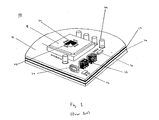
- FIG. 1 shows a prior art depiction of a CPU system ( 10 ).
- the CPU system ( 10 ) includes a printed circuit board (PCB) ( 12 ).
- the PCB ( 12 ) is a central platform on which various components are mounted.
- the PCB ( 12 ) has multiple layers that contain traces that connect the power supply and signals to the various components mounted on the PCB ( 12 ). Two layers, a system power supply layer ( 14 ) and a system ground layer ( 16 ), are shown in FIG. 1.
- the system power supply layer ( 14 ) and the system ground layer ( 16 ) provide power to a CPU ( 20 ).
- the power supplied to the CPU ( 20 ) must traverse from a DC source (not shown) and across the system power supply layer ( 14 ) and the system ground layer ( 16 ) to a package ( 18 ) on which the CPU ( 20 ) is mounted.
- Other components are also mounted on the PCB ( 12 ) that generally attempt to maintain a constant voltage supplied to the CPU ( 20 ). These components may include, but are not limited to, an air-core inductor ( 24 ), a power supply regulating integrated circuit ( 26 ), switching transistors ( 28 ), a tantalum capacitor ( 30 ), and electrolytic capacitors ( 32 ).
- the power supplied to the CPU ( 20 ) traverses from the DC source (not shown) and across the power distribution network created by the system power supply layer ( 14 ) and the system ground layer ( 16 ).
- Each layer ( 14 , 16 ) creates a plane within the PCB ( 12 ).
- Electrolytic capacitors ( 32 ) mounted on the PCB ( 12 ) connect between the system power supply layer ( 14 ) and the system ground layer ( 16 ).
- the package ( 18 ), similar to the PCB, may include multiple planes and interconnections between the planes to provide a connective substrate in which power and signals traverse.
- Ceramic capacitors ( 22 ) mounted on the package ( 18 ) connect between a system power supply (not shown) and a system ground (not shown). Ceramic capacitors ( 22 ), local to the CPU ( 20 ), may help maintain a constant voltage near the CPU ( 20 ).
- the power required by the CPU ( 20 ) changes.
- the active switching causes power supply noise.
- the addition of components attempts to minimize the power supply noise generated by the CPU.
- ceramic capacitors ( 22 ) near the CPU ( 20 ) act as local power supplies by storing charge.
- the impedance of the power distribution network may cause chip/package resonance.
- Chip/package resonance may cause oscillations in the system power supply.
- the resonances are formed by the parasitics (i.e., inductance, resistance, capacitance) included in the CPU ( 20 ) (i.e., chip, integrated circuit), package ( 18 ), and power distribution network.
- the resonance may be formed from a parasitic tank circuit that includes the chip capacitance and package inductance.
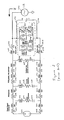
- FIG. 2 shows a prior art schematic of a power distribution network for a CPU.
- a DC power supply ( 202 ) is shown at the left.
- Two power supply lines ( 292 , 294 ) supply power to a CPU located between the two power supply lines ( 292 , 294 ).
- the circuit elements between the DC power supply ( 202 ) and the power supply lines ( 292 , 294 ) model both the inherent parasitics of the power distribution network and added components.
- the DC power supply ( 202 ) connects to the power distribution network through a power supply connector.
- the power supply connector has inherent parasitics modeled by resistors ( 204 , 208 ) and inductors ( 206 , 210 ).
- the electrolytic capacitors ( 32 in FIG. 1) are represented as bulk capacitors in FIG. 2. Capacitors do not only have a capacitive behavior but also a small resistive and inductive behavior.
- the inductor ( 212 ), resistor ( 214 ), and capacitor ( 216 ) model the bulk capacitors.
- the parasitic behavior of the PCB planes (system power supply layer ( 14 ) and system ground layer ( 16 ) in FIG. 1) is modeled as resistors ( 218 , 222 ) and inductors ( 220 , 224 ).
- the power distribution network may include multiple power supply planes and connections to a package (or multiple packages).
- the inherent series parasitics of the power distribution network are modeled by resistors ( 232 , 236 , 240 , 244 ) and inductors ( 234 , 238 , 242 , 246 ).
- Multiple planes and interconnections between the planes may create parasitics in parallel with the power supply.
- inherent parallel parasitics created by the power distribution network are modeled.
- additional capacitance in parallel with the power supply may help maintain a constant voltage.
- the additional capacitance may be connected between the power supply planes, for example, ceramic capacitors may connect between the system power supply plane and system ground plane.
- the inductance ( 226 ), resistance ( 228 ), and capacitance ( 230 ) model some of the parasitics in parallel with the power supply ( 202 ). Additional inherent parasitics and added capacitance local to the CPU may be modeled.
- the ceramic capacitors ( 22 in FIG. 1) and other inherent parasitics created by the package multiple planes and interconnections are modeled by inductor ( 248 ), resistor ( 250 ), and capacitor ( 252 ).
- a package may connect to a CPU using a grid of solder bumps.
- the inherent parasitics created by the solder bumps are modeled by inductors ( 254 , 258 ) and resistors ( 256 , 260 ).
- various forms of chip capacitance may be used to further stabilize the power supply.
- Low equivalent series resistance (ESR) local decoupling capacitors are modeled by resistor ( 262 ) and capacitor ( 264 ).
- High ESR global decoupling capacitors are modeled by resistor ( 266 ) and capacitor ( 268 ).
- Non-switching logic on the CPU is modeled by resistor ( 270 ) and capacitors ( 272 , 274 ). Switching logic on the CPU is modeled by variable resistors ( 276 , 278 ) and capacitors ( 280 , 282 ).
- the schematic of the power distribution network may be used to simulate the impedance observed by the CPU, as represented by “Z.”
- a 1 Ampere AC current source ( 290 ) injects current onto power supply line ( 292 ).
- the measured voltage, V M between two power supply lines ( 292 , 294 ) may be used to calculate the impedance.
- the impedance Z is equal to V M divided by 1 Ampere.
- a frequency versus impedance graph may be drawn. Over a particular range of frequencies, the impedance increases because the circuit formed by the chip and package resonates. The resonance from the chip and package may lead to undesirable effects on the CPU operation.
- an apparatus for reducing a power supply impedance of an integrated circuit comprises a package on which the integrated circuit is mounted; a power supply path on the package adapted to receive power from a power supply where the power supply path comprises a first power supply line and a second power supply line to provide power to the integrated circuit; and at least one resistive element connected between the first power supply line and the second power supply line where the at least one resistive element comprises a potentiometer to reduce the power supply impedance of the integrated circuit.
- a method for reducing an impedance of a power supply path of an integrated circuit where the power supply path comprises a first power supply line and a second power supply line, the method comprises determining an impedance of the power supply path of the integrated circuit, and adjusting a value of a resistance connected between the first power supply line and the second power supply line to reduce the impedance of the power supply path.
- FIG. 1 shows a prior art depiction of a central processing unit system.
- FIG. 2 shows a prior art schematic of a power distribution network for a central processing unit.
- FIG. 3 shows a schematic of a power distribution network for a central processing unit in accordance with an embodiment of the present invention.
- FIG. 4 shows a graph depicting the power supply system impedance of the circuit shown in FIGS. 2 and 3 in accordance with an embodiment of the present invention.
- Embodiments of the present invention relate to an apparatus for reducing a power supply impedance of an integrated circuit. Embodiments of the present invention further relate to a method for reducing a power supply impedance of an integrated circuit.
- embodiments of the present invention relate to reducing a power supply impedance of an integrated circuit that is connected to a power supply via two power supply lines. At least one resistive element is connected across the two power supply lines, and the at least one resistive element reduces the power supply impedance of the integrated circuit.
- the resistive element may include a resistor, potentiometer, and/or a controlled, inherent resistance from a capacitor or signal trace.
- FIG. 2 a prior art schematic of a power distribution network for a CPU is shown.
- the CPU is representative of any integrated circuit.
- the integrated circuit is powered through two power supply lines ( 292 , 294 ).
- multiple power supply lines may be used to provide adequate current capacity.
- Multiple power supply lines typically have a common source at some point in the circuit.
- a representative inductor ( 248 ), resistor ( 250 ), and capacitor ( 252 ) model the inherent parasitics created by the package and added capacitance between the two power supply lines ( 292 , 294 ). The added capacitance is used to minimize the power supply noise created by the active switching of the integrated circuit.
- the inductor ( 248 ), resistor ( 250 ), and capacitor ( 252 ) in parallel with the integrated circuit parasitics and solder bump parasitics may form a circuit that will resonate at a frequency. The resonance, which is observed as a change in impedance, may be determined through simulation or laboratory experiments.
- a 1 Ampere AC current source ( 290 ) is used to excite the circuit shown in FIG. 2. As the frequency of the AC current source is varied, the measured voltage (V M ) between the two power supply lines ( 292 , 294 ) is measured. The impedance may be determined by dividing the measured voltage, V M , by the 1 Ampere AC current source ( 290 ) (i.e., Ohm's law).
- FIG. 4 a representative drawing of the impedance (Z) as observed by the integrated circuit in FIG. 2 at different frequencies is shown with the graph ( 402 ).
- the impedance peaks typically between 10 MHz and 100 MHz.
- the inherent parasitics of the integrated circuit and package on which the integrated circuit is mounted interact with the inherent parasitics and added components of the power distribution network.
- the increase in impedance as observed by the integrated circuit occurs because a circuit created by the integrated circuit and package resonates.
- the inductor ( 248 ), resistor ( 250 ), and capacitor ( 252 ) that model the parasitics of the package may have a large effect on the amount of resonance.
- the inherent parasitics and added components are similar to the inherent parasitics and added components shown in FIG. 2.
- the resistor ( 350 ) that models the resistance included in the package inductance ( 348 ), resistance ( 350 ), and capacitance ( 352 ) may be used to reduce the chip/package resonance.
- the inductance ( 348 ), resistance ( 350 ), and capacitance ( 352 ) are the result of inherent and added parasitics from a power supply path on the package.
- the parasitics from the package included package vias (connections between power supply traces) and package planes.
- the package may include signal and power connection created by using signal and power supply traces.
- the signal and power supply traces may be arranged in planes. The planes may connect to other planes using vias.
- the inductance ( 348 ), resistance ( 350 ), and capacitance ( 352 ) are also the result of added capacitors on the package.
- the resistance ( 250 ) is designed to be low to allow the on-chip capacitor, for example the ceramic capacitors ( 22 in FIG. 1) near the CPU ( 20 in FIG. 1), to quickly respond to any power supply noise.
- the parasitic tank circuit may increase the impedance through chip/package resonance.
- the graph ( 402 ) has a high Q factor, or quality factor.
- the quality of a signal, or Q factor is a measure of the signal's maximum compared to the signal's width.
- a low Q factor is desirable because a low impedance improves the current flow to an integrated circuit.
- FIG. 3 the resistance ( 350 ) is increased compared to the resistance ( 250 ) in FIG. 2.
- An appropriately selected value for the resistance ( 350 ) changes the chip/package resonance.
- FIG. 4 displays a representative graph ( 404 ) of the impedance as observed by the integrated circuit at Z in FIG. 3 at different frequencies using an appropriately selected value for the resistance ( 350 ).
- the graph ( 404 ) of the impedance has a reduced peak compared to graph ( 402 ).
- the increased resistance ( 350 ) creates a damping effect on the amount of resonance.
- An increase in the resistance value of the resistive element ( 350 in FIG. 3) will reduce the peak (Q factor) of the impedance Z observed by the integrated circuit.
- the resistance ( 350 ), or resistive element may be a resistance formed from a resistor or potentiometer.
- the resistance ( 350 ), or resistive element may also be formed from the equivalent series resistance that is inherent in a capacitor.
- the resistance ( 350 ), or resistive element may further be formed from the power supply traces (or connections) that connect components (e.g., resistors, inductors, capacitors) to the power distribution network, the package, and ultimately to the integrated circuit. Resistance of a power supply trace may adjusted by selecting or varying the width, thickness, length, and/or metallurgical properties of the power supply trace. Also, the number of traces and the number of connections (e.g., vias) between traces on different planes may be used to select the resistance.
- the resistance ( 350 ), or resistive element connects between two power supply lines.
- a power supply line may be composed of multiple power supply traces. Each power supply trace may have a similar voltage and may originate from a common source.
- the resistance ( 350 ) may be connected to any of the multiple power supply traces to create a connection to the power supply line.
- selecting an appropriate resistance may include considering the contribution of several resistive elements.
- the method of selecting an appropriate resistance may occur through simulation, adjustment of a circuit element, and/or selection of a resistance from several preset values. The selection may occur in the design process or at the time of manufacture.
- Advantages of the present invention may include one or more of the following.
- the chip/package peak impedance may be reduced.
- a capacitor with a higher equivalent series inductance may be used with a resistive element that dampens the peak impedance created by the increased inductance.
- the capacitor with a higher equivalent series inductance may be less expensive than the capacitor with a lower equivalent series inductance.
- a value of the resistive element may be selected using simulation.
- the value of the resistive element may be selected as part of the manufacture of the package.
- the value of the resistive element may be selected after measuring parameters from the integrated circuit, integrated circuit package, and/or power distribution network.
Landscapes
- Semiconductor Integrated Circuits (AREA)
Abstract
Description
- Power supplied to a central processing unit (CPU) occurs through a power distribution network. The power distribution network starts with a power supply that generates an appropriate DC voltage. The power supplied to the CPU must traverse from the power supply and across the power distribution network before it reaches the CPU. The power distribution network has characteristics that may affect the operation of the CPU.
- FIG. 1 shows a prior art depiction of a CPU system ( 10). The CPU system (10) includes a printed circuit board (PCB) (12). The PCB (12) is a central platform on which various components are mounted. The PCB (12) has multiple layers that contain traces that connect the power supply and signals to the various components mounted on the PCB (12). Two layers, a system power supply layer (14) and a system ground layer (16), are shown in FIG. 1.
- The system power supply layer ( 14) and the system ground layer (16) provide power to a CPU (20). The power supplied to the CPU (20) must traverse from a DC source (not shown) and across the system power supply layer (14) and the system ground layer (16) to a package (18) on which the CPU (20) is mounted. Other components are also mounted on the PCB (12) that generally attempt to maintain a constant voltage supplied to the CPU (20). These components may include, but are not limited to, an air-core inductor (24), a power supply regulating integrated circuit (26), switching transistors (28), a tantalum capacitor (30), and electrolytic capacitors (32).
- In FIG. 1, the power supplied to the CPU ( 20) traverses from the DC source (not shown) and across the power distribution network created by the system power supply layer (14) and the system ground layer (16). Each layer (14, 16) creates a plane within the PCB (12). A variety of different types and different locations of capacitors are used to help maintain a constant voltage supplied to the CPU (20). Electrolytic capacitors (32) mounted on the PCB (12) connect between the system power supply layer (14) and the system ground layer (16). The package (18), similar to the PCB, may include multiple planes and interconnections between the planes to provide a connective substrate in which power and signals traverse. Ceramic capacitors (22) mounted on the package (18) connect between a system power supply (not shown) and a system ground (not shown). Ceramic capacitors (22), local to the CPU (20), may help maintain a constant voltage near the CPU (20).
- Due to active switching of circuit elements on the CPU ( 20), the power required by the CPU (20) changes. The active switching causes power supply noise. The addition of components attempts to minimize the power supply noise generated by the CPU. For example, ceramic capacitors (22) near the CPU (20) act as local power supplies by storing charge. Although the addition of components helps reduce the power supply noise, the impedance of the power distribution network may cause chip/package resonance. Chip/package resonance may cause oscillations in the system power supply. The resonances are formed by the parasitics (i.e., inductance, resistance, capacitance) included in the CPU (20) (i.e., chip, integrated circuit), package (18), and power distribution network. In particular, the resonance may be formed from a parasitic tank circuit that includes the chip capacitance and package inductance.
- FIG. 2 shows a prior art schematic of a power distribution network for a CPU. A DC power supply ( 202) is shown at the left. Two power supply lines (292, 294) supply power to a CPU located between the two power supply lines (292, 294). The circuit elements between the DC power supply (202) and the power supply lines (292, 294) model both the inherent parasitics of the power distribution network and added components.
- In FIG. 2, the DC power supply ( 202) connects to the power distribution network through a power supply connector. The power supply connector has inherent parasitics modeled by resistors (204, 208) and inductors (206, 210). The electrolytic capacitors (32 in FIG. 1) are represented as bulk capacitors in FIG. 2. Capacitors do not only have a capacitive behavior but also a small resistive and inductive behavior. The inductor (212), resistor (214), and capacitor (216) model the bulk capacitors. The parasitic behavior of the PCB planes (system power supply layer (14) and system ground layer (16) in FIG. 1) is modeled as resistors (218, 222) and inductors (220, 224).
- In FIG. 2, the power distribution network may include multiple power supply planes and connections to a package (or multiple packages). The inherent series parasitics of the power distribution network are modeled by resistors ( 232, 236, 240, 244) and inductors (234, 238, 242, 246).
- Multiple planes and interconnections between the planes may create parasitics in parallel with the power supply. In FIG. 2, inherent parallel parasitics created by the power distribution network are modeled. Also, additional capacitance in parallel with the power supply may help maintain a constant voltage. The additional capacitance may be connected between the power supply planes, for example, ceramic capacitors may connect between the system power supply plane and system ground plane. The inductance ( 226), resistance (228), and capacitance (230) model some of the parasitics in parallel with the power supply (202). Additional inherent parasitics and added capacitance local to the CPU may be modeled. The ceramic capacitors (22 in FIG. 1) and other inherent parasitics created by the package multiple planes and interconnections are modeled by inductor (248), resistor (250), and capacitor (252).
- A package may connect to a CPU using a grid of solder bumps. In FIG. 2, the inherent parasitics created by the solder bumps are modeled by inductors ( 254, 258) and resistors (256, 260). On the CPU, various forms of chip capacitance may be used to further stabilize the power supply. Low equivalent series resistance (ESR) local decoupling capacitors are modeled by resistor (262) and capacitor (264). High ESR global decoupling capacitors are modeled by resistor (266) and capacitor (268). Non-switching logic on the CPU is modeled by resistor (270) and capacitors (272, 274). Switching logic on the CPU is modeled by variable resistors (276, 278) and capacitors (280, 282).
- In FIG. 2, the schematic of the power distribution network may be used to simulate the impedance observed by the CPU, as represented by “Z.” To simulate the impedance, a 1 Ampere AC current source ( 290) injects current onto power supply line (292). The measured voltage, VM, between two power supply lines (292, 294) may be used to calculate the impedance. The impedance Z is equal to VM divided by 1 Ampere. By varying the frequency of the 1 Ampere AC current source (290), a frequency versus impedance graph may be drawn. Over a particular range of frequencies, the impedance increases because the circuit formed by the chip and package resonates. The resonance from the chip and package may lead to undesirable effects on the CPU operation.
- According to one aspect of the present invention, an apparatus for reducing a power supply impedance of an integrated circuit comprises a package on which the integrated circuit is mounted; a power supply path on the package adapted to receive power from a power supply where the power supply path comprises a first power supply line and a second power supply line to provide power to the integrated circuit; and at least one resistive element connected between the first power supply line and the second power supply line where the at least one resistive element comprises a potentiometer to reduce the power supply impedance of the integrated circuit.
- According to one aspect of the present invention, a method for reducing an impedance of a power supply path of an integrated circuit where the power supply path comprises a first power supply line and a second power supply line, the method comprises determining an impedance of the power supply path of the integrated circuit, and adjusting a value of a resistance connected between the first power supply line and the second power supply line to reduce the impedance of the power supply path.
- Other aspects and advantages of the invention will be apparent from the following description and the appended claims.
- FIG. 1 shows a prior art depiction of a central processing unit system.
- FIG. 2 shows a prior art schematic of a power distribution network for a central processing unit.
- FIG. 3 shows a schematic of a power distribution network for a central processing unit in accordance with an embodiment of the present invention.
- FIG. 4 shows a graph depicting the power supply system impedance of the circuit shown in FIGS. 2 and 3 in accordance with an embodiment of the present invention.
- Embodiments of the present invention relate to an apparatus for reducing a power supply impedance of an integrated circuit. Embodiments of the present invention further relate to a method for reducing a power supply impedance of an integrated circuit.
- More particularly, embodiments of the present invention relate to reducing a power supply impedance of an integrated circuit that is connected to a power supply via two power supply lines. At least one resistive element is connected across the two power supply lines, and the at least one resistive element reduces the power supply impedance of the integrated circuit. The resistive element may include a resistor, potentiometer, and/or a controlled, inherent resistance from a capacitor or signal trace.
- In FIG. 2, a prior art schematic of a power distribution network for a CPU is shown. The CPU is representative of any integrated circuit. The integrated circuit is powered through two power supply lines ( 292, 294). In practice, multiple power supply lines may be used to provide adequate current capacity. Multiple power supply lines typically have a common source at some point in the circuit.
- In FIG. 2, a representative inductor ( 248), resistor (250), and capacitor (252) model the inherent parasitics created by the package and added capacitance between the two power supply lines (292, 294). The added capacitance is used to minimize the power supply noise created by the active switching of the integrated circuit. The inductor (248), resistor (250), and capacitor (252) in parallel with the integrated circuit parasitics and solder bump parasitics may form a circuit that will resonate at a frequency. The resonance, which is observed as a change in impedance, may be determined through simulation or laboratory experiments.
- To determine the impedance represented by Z observed by the integrated circuit, a 1 Ampere AC current source ( 290) is used to excite the circuit shown in FIG. 2. As the frequency of the AC current source is varied, the measured voltage (VM) between the two power supply lines (292, 294) is measured. The impedance may be determined by dividing the measured voltage, VM, by the 1 Ampere AC current source (290) (i.e., Ohm's law).
- In FIG. 4, a representative drawing of the impedance (Z) as observed by the integrated circuit in FIG. 2 at different frequencies is shown with the graph ( 402). The impedance peaks typically between 10 MHz and 100 MHz. The inherent parasitics of the integrated circuit and package on which the integrated circuit is mounted interact with the inherent parasitics and added components of the power distribution network. The increase in impedance as observed by the integrated circuit occurs because a circuit created by the integrated circuit and package resonates. The inductor (248), resistor (250), and capacitor (252) that model the parasitics of the package may have a large effect on the amount of resonance.
- In FIG. 3, the inherent parasitics and added components are similar to the inherent parasitics and added components shown in FIG. 2. According to an embodiment of the present invention, the resistor ( 350) that models the resistance included in the package inductance (348), resistance (350), and capacitance (352) may be used to reduce the chip/package resonance. The inductance (348), resistance (350), and capacitance (352) are the result of inherent and added parasitics from a power supply path on the package. The parasitics from the package included package vias (connections between power supply traces) and package planes. The package may include signal and power connection created by using signal and power supply traces. The signal and power supply traces may be arranged in planes. The planes may connect to other planes using vias. The inductance (348), resistance (350), and capacitance (352) are also the result of added capacitors on the package.
- In FIG. 2, the resistance ( 250) is designed to be low to allow the on-chip capacitor, for example the ceramic capacitors (22 in FIG. 1) near the CPU (20 in FIG. 1), to quickly respond to any power supply noise. As shown in FIG. 4 with the graph (402), however, the parasitic tank circuit may increase the impedance through chip/package resonance. The graph (402) has a high Q factor, or quality factor. The quality of a signal, or Q factor, is a measure of the signal's maximum compared to the signal's width. A low Q factor is desirable because a low impedance improves the current flow to an integrated circuit.
- In FIG. 3, the resistance ( 350) is increased compared to the resistance (250) in FIG. 2. An appropriately selected value for the resistance (350) changes the chip/package resonance. As a result of an embodiment of the present invention, FIG. 4 displays a representative graph (404) of the impedance as observed by the integrated circuit at Z in FIG. 3 at different frequencies using an appropriately selected value for the resistance (350). The graph (404) of the impedance has a reduced peak compared to graph (402). The increased resistance (350) creates a damping effect on the amount of resonance. An increase in the resistance value of the resistive element (350 in FIG. 3) will reduce the peak (Q factor) of the impedance Z observed by the integrated circuit.
- Those with ordinary skill in the art will appreciate that the resistance ( 350), or resistive element, may be a resistance formed from a resistor or potentiometer. The resistance (350), or resistive element, may also be formed from the equivalent series resistance that is inherent in a capacitor. The resistance (350), or resistive element, may further be formed from the power supply traces (or connections) that connect components (e.g., resistors, inductors, capacitors) to the power distribution network, the package, and ultimately to the integrated circuit. Resistance of a power supply trace may adjusted by selecting or varying the width, thickness, length, and/or metallurgical properties of the power supply trace. Also, the number of traces and the number of connections (e.g., vias) between traces on different planes may be used to select the resistance.
- Those with ordinary skill in the art will appreciate that the resistance ( 350), or resistive element, connects between two power supply lines. A power supply line may be composed of multiple power supply traces. Each power supply trace may have a similar voltage and may originate from a common source. The resistance (350) may be connected to any of the multiple power supply traces to create a connection to the power supply line.
- Those skilled in the art will appreciate that selecting an appropriate resistance may include considering the contribution of several resistive elements. The method of selecting an appropriate resistance may occur through simulation, adjustment of a circuit element, and/or selection of a resistance from several preset values. The selection may occur in the design process or at the time of manufacture.
- Advantages of the present invention may include one or more of the following. In some embodiments, because a resistive element is selected, the chip/package peak impedance may be reduced. A capacitor with a higher equivalent series inductance may be used with a resistive element that dampens the peak impedance created by the increased inductance. The capacitor with a higher equivalent series inductance may be less expensive than the capacitor with a lower equivalent series inductance.
- Other advantages of the present invention may include one or more of the following. A value of the resistive element may be selected using simulation. The value of the resistive element may be selected as part of the manufacture of the package. The value of the resistive element may be selected after measuring parameters from the integrated circuit, integrated circuit package, and/or power distribution network.
- While the invention has been described with respect to a limited number of embodiments, those skilled in the art, having benefit of this disclosure, will appreciate that other embodiments can be devised which do not depart from the scope of the invention as disclosed herein. Accordingly, the scope of the invention should be limited only by the attached claims.
Claims (13)
Priority Applications (1)
| Application Number | Priority Date | Filing Date | Title |
|---|---|---|---|
| US10/118,840 US6822345B2 (en) | 2002-04-09 | 2002-04-09 | Chip/package resonance damping using controlled package series resistance |
Applications Claiming Priority (1)
| Application Number | Priority Date | Filing Date | Title |
|---|---|---|---|
| US10/118,840 US6822345B2 (en) | 2002-04-09 | 2002-04-09 | Chip/package resonance damping using controlled package series resistance |
Publications (2)
| Publication Number | Publication Date |
|---|---|
| US20030197430A1 true US20030197430A1 (en) | 2003-10-23 |
| US6822345B2 US6822345B2 (en) | 2004-11-23 |
Family
ID=29214423
Family Applications (1)
| Application Number | Title | Priority Date | Filing Date |
|---|---|---|---|
| US10/118,840 Expired - Lifetime US6822345B2 (en) | 2002-04-09 | 2002-04-09 | Chip/package resonance damping using controlled package series resistance |
Country Status (1)
| Country | Link |
|---|---|
| US (1) | US6822345B2 (en) |
Cited By (7)
| Publication number | Priority date | Publication date | Assignee | Title |
|---|---|---|---|---|
| US20040088624A1 (en) * | 2002-10-22 | 2004-05-06 | Gauthier Claude R. | Method for quantifying I/O chip/package resonance |
| US7017086B2 (en) | 2002-06-18 | 2006-03-21 | Sun Microsystems, Inc. | Round-robin updating for high speed I/O parallel interfaces |
| US7043683B2 (en) | 2003-02-07 | 2006-05-09 | Sun Microsystems, Inc. | Data transmission update technique in low power modes |
| US7062688B2 (en) | 2002-07-16 | 2006-06-13 | Sun Microsystems, Inc. | Updating high speed parallel I/O interfaces based on counters |
| US20060291174A1 (en) * | 2005-06-28 | 2006-12-28 | Myat Myitzu S | Embedding thin film resistors in substrates in power delivery networks |
| WO2012078263A1 (en) * | 2010-12-07 | 2012-06-14 | Xilinx, Inc. | Power distribution network |
| CN119519418A (en) * | 2025-01-07 | 2025-02-25 | 荣耀终端股份有限公司 | A power distribution network PDN system, electronic equipment and board-level network module |
Families Citing this family (5)
| Publication number | Priority date | Publication date | Assignee | Title |
|---|---|---|---|---|
| US6963240B2 (en) * | 2003-11-25 | 2005-11-08 | International Business Machines Corporation | Damping of LC ringing in IC (integrated circuit) power distribution systems |
| CN100561844C (en) * | 2005-12-06 | 2009-11-18 | 鸿富锦精密工业(深圳)有限公司 | AC power outlet voltage divider circuit |
| US7633773B2 (en) * | 2006-05-10 | 2009-12-15 | Micron Technology, Inc. | On-die anti-resonance structure for integrated circuit |
| US8208338B2 (en) * | 2006-05-12 | 2012-06-26 | Samsung Electronics Co., Ltd. | Semiconductor device |
| TW200828795A (en) * | 2006-12-22 | 2008-07-01 | Realtek Semiconductor Corp | Circuit for inhibiting voltage jittering and method thereof |
Citations (1)
| Publication number | Priority date | Publication date | Assignee | Title |
|---|---|---|---|---|
| US5319263A (en) * | 1992-05-29 | 1994-06-07 | Eastman Kodak Company | Power saving impedance transformation circuit for CCD image sensors |
Family Cites Families (2)
| Publication number | Priority date | Publication date | Assignee | Title |
|---|---|---|---|---|
| JPS60236585A (en) * | 1984-05-10 | 1985-11-25 | Sony Corp | Control method of electronic circuit |
| JP3212555B2 (en) * | 1998-05-29 | 2001-09-25 | 沖電気工業株式会社 | Electronic inductance circuit |
-
2002
- 2002-04-09 US US10/118,840 patent/US6822345B2/en not_active Expired - Lifetime
Patent Citations (1)
| Publication number | Priority date | Publication date | Assignee | Title |
|---|---|---|---|---|
| US5319263A (en) * | 1992-05-29 | 1994-06-07 | Eastman Kodak Company | Power saving impedance transformation circuit for CCD image sensors |
Cited By (15)
| Publication number | Priority date | Publication date | Assignee | Title |
|---|---|---|---|---|
| US7017086B2 (en) | 2002-06-18 | 2006-03-21 | Sun Microsystems, Inc. | Round-robin updating for high speed I/O parallel interfaces |
| US7062688B2 (en) | 2002-07-16 | 2006-06-13 | Sun Microsystems, Inc. | Updating high speed parallel I/O interfaces based on counters |
| US20040088624A1 (en) * | 2002-10-22 | 2004-05-06 | Gauthier Claude R. | Method for quantifying I/O chip/package resonance |
| US7043379B2 (en) * | 2002-10-22 | 2006-05-09 | Sun Microsystems, Inc. | Method for quantifying I/O chip/package resonance |
| US7043683B2 (en) | 2003-02-07 | 2006-05-09 | Sun Microsystems, Inc. | Data transmission update technique in low power modes |
| WO2007002948A1 (en) * | 2005-06-28 | 2007-01-04 | Intel Corporation | Embedding thin film resistors in substrates in power delivery networks |
| US20060291174A1 (en) * | 2005-06-28 | 2006-12-28 | Myat Myitzu S | Embedding thin film resistors in substrates in power delivery networks |
| DE112006001179B4 (en) * | 2005-06-28 | 2011-01-05 | Intel Corporation, Santa Clara | Device with embedded thin film resistors in substrates in power supply networks |
| WO2012078263A1 (en) * | 2010-12-07 | 2012-06-14 | Xilinx, Inc. | Power distribution network |
| US8410579B2 (en) | 2010-12-07 | 2013-04-02 | Xilinx, Inc. | Power distribution network |
| CN103283018A (en) * | 2010-12-07 | 2013-09-04 | 吉林克斯公司 | Power distribution network |
| JP2014502428A (en) * | 2010-12-07 | 2014-01-30 | ザイリンクス インコーポレイテッド | Power distribution network |
| KR101513383B1 (en) | 2010-12-07 | 2015-04-17 | 자일링크스 인코포레이티드 | Power distribution network |
| CN103283018B (en) * | 2010-12-07 | 2016-05-04 | 吉林克斯公司 | Distribution network |
| CN119519418A (en) * | 2025-01-07 | 2025-02-25 | 荣耀终端股份有限公司 | A power distribution network PDN system, electronic equipment and board-level network module |
Also Published As
| Publication number | Publication date |
|---|---|
| US6822345B2 (en) | 2004-11-23 |
Similar Documents
| Publication | Publication Date | Title |
|---|---|---|
| US6822345B2 (en) | Chip/package resonance damping using controlled package series resistance | |
| US8023293B2 (en) | On-die anti-resonance structure for integrated circuit | |
| US6703697B2 (en) | Electronic package design with improved power delivery performance | |
| US7886431B2 (en) | Power distribution system for integrated circuits | |
| US7773390B2 (en) | Power distribution system for integrated circuits | |
| US9345126B2 (en) | Semiconductor package and printed circuit board | |
| US6842351B2 (en) | Method and apparatus for I/O resonance compensation | |
| US6781355B2 (en) | I/O power supply resonance compensation technique | |
| JP2000305968A (en) | Printed circuit board characteristic evaluation apparatus, printed circuit board characteristic evaluation method, and storage medium | |
| US8208338B2 (en) | Semiconductor device | |
| US20070279882A1 (en) | Power distribution system for integrated circuits | |
| Smith et al. | Distributed SPICE circuit model for ceramic capacitors | |
| KR20190073438A (en) | Switching regulator synchronous node snubber circuit | |
| US6700390B2 (en) | Adjustment and calibration system to store resistance settings to control chip/package resonance | |
| US6806569B2 (en) | Multi-frequency power delivery system | |
| US6606012B2 (en) | Wideband bypass capacitor methods for achieving a desired value of electrical impedance between parallel planar conductors of an electrical power distribution structure | |
| US20180317316A1 (en) | Reduction of passive components in system-in-package devices | |
| US8332790B1 (en) | Capacitive decoupling method and module | |
| US10355661B1 (en) | Anti-resonance structure for dampening die package resonance | |
| CN100555626C (en) | Semiconductor device, related method and printed circuit board | |
| US9078354B2 (en) | Techniques for attenuating resonance induced impedance in integrated circuits | |
| US7843979B2 (en) | Damping of parasitic resonance using a resistive parallel conductor | |
| Powers et al. | Comprehensive PDN/PSIJ analysis of silicon capacitor use for 8.533 GT/s LPDDR5X application | |
| US20030046594A1 (en) | Power delivery system and method for setting power delivery system parameters | |
| Chase | Introduction to Choosing MLC Capacitors for bypass/decoupling applications |
Legal Events
| Date | Code | Title | Description |
|---|---|---|---|
| AS | Assignment |
Owner name: SUN MICROSYSTEM, INC., CALIFORNIA Free format text: ASSIGNMENT OF ASSIGNORS INTEREST;ASSIGNORS:GAUTHIER, CLAUDE;AMICK, BRIAN;REEL/FRAME:012788/0882;SIGNING DATES FROM 20020405 TO 20020407 |
|
| STCF | Information on status: patent grant |
Free format text: PATENTED CASE |
|
| FPAY | Fee payment |
Year of fee payment: 4 |
|
| FPAY | Fee payment |
Year of fee payment: 8 |
|
| FPAY | Fee payment |
Year of fee payment: 12 |
|
| AS | Assignment |
Owner name: ORACLE AMERICA, INC., CALIFORNIA Free format text: MERGER AND CHANGE OF NAME;ASSIGNORS:ORACLE USA, INC.;SUN MICROSYSTEMS, INC.;ORACLE AMERICA, INC.;REEL/FRAME:039888/0635 Effective date: 20100212 |
|
| AS | Assignment |
Owner name: ORGANIZATION - WORLD INTELLECTUAL PROPERTY, LOUISIANA Free format text: MERGER AND CHANGE OF NAME;ASSIGNORS:UNITED STATES OF AMERICA;ORGANIZATION - WORLD INTELLECTUAL PROPERTY;REEL/FRAME:056813/0485 Effective date: 19650115 |