US20030193760A1 - Thin film head with transverse biasing layers - Google Patents
Thin film head with transverse biasing layers Download PDFInfo
- Publication number
- US20030193760A1 US20030193760A1 US10/413,735 US41373503A US2003193760A1 US 20030193760 A1 US20030193760 A1 US 20030193760A1 US 41373503 A US41373503 A US 41373503A US 2003193760 A1 US2003193760 A1 US 2003193760A1
- Authority
- US
- United States
- Prior art keywords
- layer
- layers
- nonmagnetic
- pair
- free magnetic
- Prior art date
- Legal status (The legal status is an assumption and is not a legal conclusion. Google has not performed a legal analysis and makes no representation as to the accuracy of the status listed.)
- Granted
Links
- 239000010409 thin film Substances 0.000 title claims abstract description 106
- 230000005291 magnetic effect Effects 0.000 claims abstract description 258
- 230000005294 ferromagnetic effect Effects 0.000 claims abstract description 164
- 230000005290 antiferromagnetic effect Effects 0.000 claims abstract description 136
- 238000000034 method Methods 0.000 claims description 96
- 238000004519 manufacturing process Methods 0.000 claims description 67
- 230000005415 magnetization Effects 0.000 claims description 39
- 239000000696 magnetic material Substances 0.000 claims description 26
- 238000010438 heat treatment Methods 0.000 claims description 16
- 239000000470 constituent Substances 0.000 claims description 13
- 239000011810 insulating material Substances 0.000 claims description 8
- 238000004140 cleaning Methods 0.000 claims description 6
- 230000003064 anti-oxidating effect Effects 0.000 claims 2
- 239000000463 material Substances 0.000 description 23
- 238000010168 coupling process Methods 0.000 description 16
- 238000005859 coupling reaction Methods 0.000 description 16
- 238000001312 dry etching Methods 0.000 description 15
- 229910045601 alloy Inorganic materials 0.000 description 14
- 239000000956 alloy Substances 0.000 description 14
- 230000000694 effects Effects 0.000 description 12
- 239000004020 conductor Substances 0.000 description 10
- 238000000137 annealing Methods 0.000 description 9
- VYPSYNLAJGMNEJ-UHFFFAOYSA-N Silicium dioxide Chemical compound O=[Si]=O VYPSYNLAJGMNEJ-UHFFFAOYSA-N 0.000 description 6
- 229910052804 chromium Inorganic materials 0.000 description 5
- 229910052802 copper Inorganic materials 0.000 description 5
- 229910052715 tantalum Inorganic materials 0.000 description 5
- 230000007797 corrosion Effects 0.000 description 4
- 238000005260 corrosion Methods 0.000 description 4
- 229910017083 AlN Inorganic materials 0.000 description 3
- 230000005330 Barkhausen effect Effects 0.000 description 3
- 229910003321 CoFe Inorganic materials 0.000 description 3
- 229910015136 FeMn Inorganic materials 0.000 description 3
- 229910001030 Iron–nickel alloy Inorganic materials 0.000 description 3
- 229910019041 PtMn Inorganic materials 0.000 description 3
- PNEYBMLMFCGWSK-UHFFFAOYSA-N aluminium oxide Inorganic materials [O-2].[O-2].[O-2].[Al+3].[Al+3] PNEYBMLMFCGWSK-UHFFFAOYSA-N 0.000 description 3
- 229910052681 coesite Inorganic materials 0.000 description 3
- 229910052593 corundum Inorganic materials 0.000 description 3
- 229910052906 cristobalite Inorganic materials 0.000 description 3
- 229910000889 permalloy Inorganic materials 0.000 description 3
- 230000035945 sensitivity Effects 0.000 description 3
- 239000000377 silicon dioxide Substances 0.000 description 3
- 229910052682 stishovite Inorganic materials 0.000 description 3
- 239000000126 substance Substances 0.000 description 3
- 229910052905 tridymite Inorganic materials 0.000 description 3
- 229910001845 yogo sapphire Inorganic materials 0.000 description 3
- 239000002885 antiferromagnetic material Substances 0.000 description 2
- 238000000992 sputter etching Methods 0.000 description 2
- 229910018979 CoPt Inorganic materials 0.000 description 1
- 229910000640 Fe alloy Inorganic materials 0.000 description 1
- 229910003289 NiMn Inorganic materials 0.000 description 1
- 230000015572 biosynthetic process Effects 0.000 description 1
- 230000001419 dependent effect Effects 0.000 description 1
- 230000006866 deterioration Effects 0.000 description 1
- 238000005530 etching Methods 0.000 description 1
- 239000003302 ferromagnetic material Substances 0.000 description 1
- 229910052737 gold Inorganic materials 0.000 description 1
- 230000001939 inductive effect Effects 0.000 description 1
- 238000003780 insertion Methods 0.000 description 1
- 230000037431 insertion Effects 0.000 description 1
- 239000002184 metal Substances 0.000 description 1
- 229910052751 metal Inorganic materials 0.000 description 1
- 229910044991 metal oxide Inorganic materials 0.000 description 1
- 150000004706 metal oxides Chemical class 0.000 description 1
- 229920002120 photoresistant polymer Polymers 0.000 description 1
- 229910052709 silver Inorganic materials 0.000 description 1
- 238000004544 sputter deposition Methods 0.000 description 1
- 239000000758 substrate Substances 0.000 description 1
Images


Classifications
-
- G—PHYSICS
- G11—INFORMATION STORAGE
- G11B—INFORMATION STORAGE BASED ON RELATIVE MOVEMENT BETWEEN RECORD CARRIER AND TRANSDUCER
- G11B5/00—Recording by magnetisation or demagnetisation of a record carrier; Reproducing by magnetic means; Record carriers therefor
- G11B5/127—Structure or manufacture of heads, e.g. inductive
- G11B5/33—Structure or manufacture of flux-sensitive heads, i.e. for reproduction only; Combination of such heads with means for recording or erasing only
- G11B5/39—Structure or manufacture of flux-sensitive heads, i.e. for reproduction only; Combination of such heads with means for recording or erasing only using magneto-resistive devices or effects
- G11B5/3903—Structure or manufacture of flux-sensitive heads, i.e. for reproduction only; Combination of such heads with means for recording or erasing only using magneto-resistive devices or effects using magnetic thin film layers or their effects, the films being part of integrated structures
- G11B5/3906—Details related to the use of magnetic thin film layers or to their effects
- G11B5/3929—Disposition of magnetic thin films not used for directly coupling magnetic flux from the track to the MR film or for shielding
- G11B5/3932—Magnetic biasing films
-
- G—PHYSICS
- G11—INFORMATION STORAGE
- G11B—INFORMATION STORAGE BASED ON RELATIVE MOVEMENT BETWEEN RECORD CARRIER AND TRANSDUCER
- G11B5/00—Recording by magnetisation or demagnetisation of a record carrier; Reproducing by magnetic means; Record carriers therefor
- G11B5/127—Structure or manufacture of heads, e.g. inductive
- G11B5/33—Structure or manufacture of flux-sensitive heads, i.e. for reproduction only; Combination of such heads with means for recording or erasing only
- G11B5/39—Structure or manufacture of flux-sensitive heads, i.e. for reproduction only; Combination of such heads with means for recording or erasing only using magneto-resistive devices or effects
- G11B5/3903—Structure or manufacture of flux-sensitive heads, i.e. for reproduction only; Combination of such heads with means for recording or erasing only using magneto-resistive devices or effects using magnetic thin film layers or their effects, the films being part of integrated structures
-
- G—PHYSICS
- G11—INFORMATION STORAGE
- G11B—INFORMATION STORAGE BASED ON RELATIVE MOVEMENT BETWEEN RECORD CARRIER AND TRANSDUCER
- G11B5/00—Recording by magnetisation or demagnetisation of a record carrier; Reproducing by magnetic means; Record carriers therefor
- G11B2005/0002—Special dispositions or recording techniques
- G11B2005/0005—Arrangements, methods or circuits
- G11B2005/001—Controlling recording characteristics of record carriers or transducing characteristics of transducers by means not being part of their structure
- G11B2005/0013—Controlling recording characteristics of record carriers or transducing characteristics of transducers by means not being part of their structure of transducers, e.g. linearisation, equalisation
- G11B2005/0016—Controlling recording characteristics of record carriers or transducing characteristics of transducers by means not being part of their structure of transducers, e.g. linearisation, equalisation of magnetoresistive transducers
-
- Y—GENERAL TAGGING OF NEW TECHNOLOGICAL DEVELOPMENTS; GENERAL TAGGING OF CROSS-SECTIONAL TECHNOLOGIES SPANNING OVER SEVERAL SECTIONS OF THE IPC; TECHNICAL SUBJECTS COVERED BY FORMER USPC CROSS-REFERENCE ART COLLECTIONS [XRACs] AND DIGESTS
- Y10—TECHNICAL SUBJECTS COVERED BY FORMER USPC
- Y10T—TECHNICAL SUBJECTS COVERED BY FORMER US CLASSIFICATION
- Y10T29/00—Metal working
- Y10T29/49—Method of mechanical manufacture
- Y10T29/49002—Electrical device making
- Y10T29/4902—Electromagnet, transformer or inductor
- Y10T29/49021—Magnetic recording reproducing transducer [e.g., tape head, core, etc.]
- Y10T29/49032—Fabricating head structure or component thereof
- Y10T29/49036—Fabricating head structure or component thereof including measuring or testing
- Y10T29/49043—Depositing magnetic layer or coating
- Y10T29/49044—Plural magnetic deposition layers
-
- Y—GENERAL TAGGING OF NEW TECHNOLOGICAL DEVELOPMENTS; GENERAL TAGGING OF CROSS-SECTIONAL TECHNOLOGIES SPANNING OVER SEVERAL SECTIONS OF THE IPC; TECHNICAL SUBJECTS COVERED BY FORMER USPC CROSS-REFERENCE ART COLLECTIONS [XRACs] AND DIGESTS
- Y10—TECHNICAL SUBJECTS COVERED BY FORMER USPC
- Y10T—TECHNICAL SUBJECTS COVERED BY FORMER US CLASSIFICATION
- Y10T29/00—Metal working
- Y10T29/49—Method of mechanical manufacture
- Y10T29/49002—Electrical device making
- Y10T29/4902—Electromagnet, transformer or inductor
- Y10T29/49021—Magnetic recording reproducing transducer [e.g., tape head, core, etc.]
- Y10T29/49032—Fabricating head structure or component thereof
- Y10T29/49067—Specified diverse magnetic materials
-
- Y—GENERAL TAGGING OF NEW TECHNOLOGICAL DEVELOPMENTS; GENERAL TAGGING OF CROSS-SECTIONAL TECHNOLOGIES SPANNING OVER SEVERAL SECTIONS OF THE IPC; TECHNICAL SUBJECTS COVERED BY FORMER USPC CROSS-REFERENCE ART COLLECTIONS [XRACs] AND DIGESTS
- Y10—TECHNICAL SUBJECTS COVERED BY FORMER USPC
- Y10T—TECHNICAL SUBJECTS COVERED BY FORMER US CLASSIFICATION
- Y10T29/00—Metal working
- Y10T29/49—Method of mechanical manufacture
- Y10T29/49002—Electrical device making
- Y10T29/49117—Conductor or circuit manufacturing
- Y10T29/49124—On flat or curved insulated base, e.g., printed circuit, etc.
- Y10T29/49155—Manufacturing circuit on or in base
Definitions
- the present invention relates to a magnetoresistive thin film head for use in hard disk drives (HDD) or such other magnetic recording apparatus which record signals on magnetic recording media in high density, and reproduce the signals therefrom; specifically, the magnetoresistive thin film head in which stable biasing magnetic fields are provided on a free magnetic layer of a magnetoresistive element, for yielding a high reproducing efficiency.
- the present invention relates also to the method for manufacturing the magnetoresistive thin film head.
- HDD magnetic disk apparatus
- other magnetic recording apparatus the needs for higher processing speed and greater recording capacity are increasing among the magnetic disk apparatus (hereinafter collectively referred to as HDD) and other magnetic recording apparatus, and quite a number of efforts are being made for increasing the recording density.
- the HDDs employ a thin film head, which head consisting of an inductive head for recording, and a magnetoresistive head (MR head), or a giant MR head (GMR head), for reproducing the signals.
- MR head magnetoresistive head
- GMR head giant MR head
- FIG. 23 is a perspective view showing outline at the sliding surface of a conventional thin film head facing a recording medium.
- FIG. 24 shows an outline view of the thin film head in the front.
- a lower gap layer 232 of Al 2 O 3 , AlN, SiO 2 , or other nonmagnetic insulating material is formed on a lower magnetic shield layer 231 made of a soft magnetic material such as Permalloy, a Co amorphous magnetic layer, an Fe alloy magnetic layer.
- a magnetoresistive element 233 an MR element or a GMR element, hereinafter both are collectively referred to as GMR element
- GMR element magnetoresistive element
- a transverse biasing layer 234 is formed by a CoPt alloy or other such magnetic material at both of the right and the left ends of the GMR element 233 .
- a lead layer 235 of conductive material such as Cu, Cr, Ta, etc. is provided on the upper surface of the transverse biasing layer 234 so that the lead layer 235 makes contact with a ridge line formed by the upper surface of the GMR element 233 and the end face.
- the lead layer 235 may be disposed on the upper surface of the transverse biasing layer 234 so that it covers part of the upper surface of the GMR element 233 .
- an upper gap layer 236 is formed over the lead layer 235 and the exposed region of the GMR element 233 , using the same nonmagnetic insulating material as the lower gap layer 232 .
- an upper magnetic shield layer 237 is provided using the same soft magnetic material as the lower magnetic shield layer 231 . This completes the reproducing part 238 of magnetoresistive head.
- a recording gap layer 241 is formed using the same nonmagnetic insulating material as the lower gap layer 232 .
- An upper magnetic core 242 which faces ⁇ to the upper magnetic shield layer 237 via the recording gap layer 241 and makes contact with the upper magnetic shield layer 237 at the rear scene of FIG. 23, is provided in the form of a layer using a soft magnetic material.
- a coil 243 is provided electrically isolated from both the upper magnetic shield layer 237 and the upper magnetic core 242 . This completes the recording part 240 of a magnetoresistive thin film head.
- the upper magnetic shield layer 237 works as the shield for the reproducing part 238 and as the lower magnetic core of the recording part 240 .
- FIG. 24 shows outline view in the front of the reproducing part at the vicinity of magetoresistive element of the above-described thin film head.
- a lower gap layer 232 is provided on the upper surface of the lower magnetic shield layer 231 .
- a magnetic material such as an FeMn alloy, a PtMn alloy
- the laminated body of stacked layers is defined at both the right and the left ends by ion-milling or the like method so that each of the cut ends has a slant surface.
- a GMR element 233 is provided.
- a pair of transverse biasing layers 234 are formed at both ends of the GMR element 233 in physical contact with the slant end surfaces, and a pair of the right and the left lead layers 235 are provided on the transverse biasing layers 234 .
- an upper gap layer 236 is formed, followed by upper magnetic shield layer 237 .
- Gap length 249 of the reproducing part 238 which represents a total sum in the thickness of the lower gap layer 232 , the GMR element 133 , and the upper gap layer 236 , takes a very small value, so that it is capable of reproducing the short-wavelength signals of high density recording.
- Recording current supplied to the coil 243 generates recording magnetic fields in the recording gap layer 241 disposed between the upper magnetic core 242 and the upper magnetic shield layer 237 of the recording head 240 , for recording the signals on a magnetic recording medium.
- the reproducing head 238 detects signal magnetic fields from a magnetic recording medium storing the signals, and signals reproduced by the GMR element 233 in accordance with the resistance change are taken out through the terminal of lead layer 235 .
- gap length of a reproducing head needs to be sufficiently short.
- the gap length is a distance between the upper surface of the lower magnetic shield layer and the lower surface of the upper magnetic shield layer. It means that the distance is represented by a total thickness of lower gap layer, the GMR element, and the upper gap layer.
- the short distance means that a pair of transverse biasing layers disposed at both the right and the left ends of the GMR element are existing very close to the lower magnetic shield layer or the upper magnetic shield layer. Under such circumstance, magnetic fields of the transverse biasing layers easily escape to the lower magnetic shield layer or the upper magnetic shield layer.
- the biasing magnetic field, applied to the free magnetic layer of GMR element becomes weak.
- the direction of magnetization of the free magnetic layer is not orientated in a stable manner, and the noise increases, making it difficult to obtain stable reproducing signals.
- the present invention addresses the above described drawbacks, and aims to make the orientation of magnetizing direction in the free magnetic layer stabilized, by providing the free magnetic layer of GMR element with accurate and stabilized biasing magnetic fields generated from the transverse biasing layers. By so doing, superior magnetoresistive head, having suppressed Barkhausen noise and superior reproducing characteristics, can be offered.
- the present invention also contains in it a method for manufacturing the magnetoresistive head.
- the thin film head of the present invention comprises a magnetoresistive element formed of an antiferromagnetic layer, a pinning layer, a nonmagnetic conductive layer and a free magnetic layer, and a pair of the right and the left laminated transverse biasing layers, each consisting of a nonmagnetic layer, a ferromagnetic layer and an antiferromagnetic layer, formed on the free magnetic layer of the magnetoresistive element.
- the layer thickness of nonmagnetic layer has been established to a certain specific value so that magnetization directions of the free magnetic layer and ferromagnetic layer, which are facing via nonmagnetic layer, are opposite each other.
- FIG. 1 Front view showing the outline structure of a thin film head in accordance with a first exemplary embodiment of the present invention.
- FIG. 2 Front view showing the outline structure of a thin film head in accordance with a second exemplary embodiment of the present invention.
- FIG. 3 Front outline view used to describe part of the process for manufacturing a thin film head in accordance with a third exemplary embodiment of the present invention.
- FIG. 4 Front outline view used to describe a first process step for manufacturing a thin film head in accordance with a third exemplary embodiment of the present invention.
- FIG. 5 Front outline view used to describe a second and a third process steps for manufacturing a thin film head in accordance with a third exemplary embodiment of the present invention.
- FIG. 6 Front outline view used to describe a fourth process step and other process step for manufacturing a thin film head in accordance with a third exemplary embodiment of the present invention.
- FIG. 7 Front outline view used to describe a second and a third process steps for manufacturing a thin film head in accordance with other example of a third exemplary embodiment of the present invention.
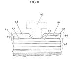
- FIG. 8 Front outline view used to describe a second process step for manufacturing a thin film head in accordance with other example of a third exemplary embodiment of the present invention.
- FIG. 9 Front outline view used to describe a third process step for manufacturing a thin film head in accordance with other example of a third exemplary embodiment of the present invention.
- FIG. 10 Front outline view used to describe a third process step for manufacturing a thin film head in accordance with other example of a third exemplary embodiment of the present invention.
- FIG. 11 Front outline view used to describe a third process step for manufacturing a thin film head in accordance with other example of a third exemplary embodiment of the present invention.
- FIG. 12 Front outline view used to describe part of a second process step for manufacturing a thin film head in accordance with a fourth exemplary embodiment of the present invention.
- FIG. 13 Front outline view used to describe other part of a second process step for manufacturing a thin film head in accordance with a fourth exemplary embodiment of the present invention.
- FIG. 14 Front outline view used to describe a third and a fourth process steps for manufacturing a thin film head in accordance with a fourth exemplary embodiment of the present invention.
- FIG. 15 Front outline view used to describe a second process step for manufacturing a thin film head in accordance with other example of a fourth exemplary embodiment of the present invention.
- FIG. 16 Front outline view used to describe a second process step for manufacturing a thin film head in accordance with other example of a fourth exemplary embodiment of the present invention.
- FIG. 17 Front outline view used to describe a third process step for manufacturing a thin film head in accordance with other example of a fourth exemplary embodiment of the present invention.
- FIG. 18 Front outline view used to describe a third process step for manufacturing a thin film head in accordance with other example of a fourth exemplary embodiment of the present invention.
- FIG. 19 Front outline view used to describe a second process step for manufacturing a thin film head in accordance with other example of a fourth exemplary embodiment of the present invention.
- FIG. 20 Front outline view used to describe a first, a second and a third process steps for manufacturing a thin film head in accordance with a fifth exemplary embodiment of the present invention.
- FIG. 21 Front outline view used to describe a second process step for manufacturing a thin film head in accordance with other example of a fifth exemplary embodiment of the present invention.
- FIG. 22 Front outline view used to describe a third process step for manufacturing a thin film head in accordance with other example of a fifth exemplary embodiment of the present invention.
- FIG. 23 Perspective view showing outline of a conventional thin film head.
- FIG. 24 Front outline view showing the structure of a conventional thin film head.
- FIG. 1 A first exemplary embodiment of the present invention is described referring to FIG. 1.
- FIG. 1 shows the structural concept of embodiment 1 of the present invention; a portion in the vicinity of the magnetoresistive element as viewed from the sliding surface facing to a magnetic recording medium.
- a lower magnetic shield layer (not shown) formed of a soft magnetic material such as Permalloy, a Co amorphous magnetic layer, an Fe fine grain magnetic layer, a lower gap layer (not shown) of Al 2 O 3 , AlN, SiO 2 , or other nonmagnetic insulating material is formed.
- MR element magnetoresistive element 5
- a pair of the right and the left laminated transverse biasing layers 9 are provided, each consisting of a nonmagnetic layer 6 of Ru or other nonmagnetic material, a ferromagnetic layer 7 of the same magnetic material as the free magnetic layer 4 and an antiferromagnetic layer 8 of the same antiferromagnetic material as the antifirromagnetic layer 1 (depending on situation, it is preferred not to use an oxidized metal). Magnetization direction of the ferromagnetic layers 7 is orientated to a certain specific direction and kept in a stable state by the effect of exchange-coupling magnetic fields with the antiferromagnetic layer 8 .
- the magnetization direction in the free magnetic layer 4 which is facing to the ferromagnetic layer 7 via the nonmagnetic layer 6 , is maintained in a quite stable state, either in the same direction or in the opposite direction reflecting the layer thickness of the interposing nonmagnetic layer 6 .
- a pair of the right and the left lead layers 10 of nonmagnetic conductive material such as Cu, Cr, Ta, are provided on the top.
- an upper gap layer (not shown) is formed using the like insulating material as the lower gap layer covering the entire area.
- an upper magnetic shield layer is formed using the same soft magnetic material as the lower magnetic shield layer to constitute the reproducing part of the thin film head of the present invention.
- a cap layer may be formed using Ta or other nonmagnetic material covering the pair of lead layers 10 and the exposed region of free magnetic layer 4 .
- magnetizing direction in the pair of the right and the left ferromagnetic layers 7 which being constituent of the laminated transverse biasing layers 9 , is made to be approximately perpendicular to that of the pinning layer 2 (direction X or direction ⁇ X, in FIG. 1 ).
- Material for the antiferromagnetic layer 8 needs to be selected among those magnetic materials whose annealing conditions for establishing magnetizing direction of the ferromagnetic layer 7 differs in at least one item of the conditions (strength of magnetic field, temperature, or process time) from annealing conditions for pinning layer 2 .
- Thickness of nonmagnetic layers 6 which being constituent of the pair of the laminated transverse biasing layers 9 , is determined so that the magnetization direction of free magnetic layer 4 becomes opposite to that of the ferromagnetic layer 7 due to the strong exchange-coupling magnetic field generated between both layers.
- the free magnetic layer 4 assumes the same magnetization direction as the ferromagnetic layer 7 .
- the nonmagnetic layer 6 is too thick the free magnetic layer 4 returns to assume the initial magnetization direction, namely the same magnetization direction as that of the ferromagnetic layer 7 . In this way, the direction of magnetization cyclically changes assuming the same and opposite directions, and strength of the exchange-coupling magnetic fields gradually reduces. Therefore, thickness of the nonmagnetic layer 6 needs to be determined within an appropriate range.
- the appropriate layer thickness for the nonmagnetic layer 6 is dependent on the kind of nonmagnetic materials used.
- the optimum value found out for each of the materials is as shown in Table 1 below.
- TABLE 1 Layer thickness for reversing the Nonmagnetic material used direction of magnetization RU 0.4-0.8 nm Cu Vicinity 0.9 nm, vicinity 2.0 nm Ag, Au 2-nm Ir Vicinity 1.3 nm
- a cap layer 11 may be provided using Ta or other nonmagnetic material, on the upper surface of the free magnetic layer 4 , in a region between the pair of the right and the left transverse biasing layers 9 .
- a pair of the right and the left laminated transverse biasing layers are formed on the free magnetic layer of GMR element via nonmagnetic layer. Magnetization direction of ferromagnetic layer is fixed to specific direction (direction ⁇ X) by annealing process.
- ⁇ X specific direction
- free magnetic layer of GMR element and said ferromagnetic layer are antiferromagnetically coupled by the effect of exchange-coupling magnetic field, and magnetization direction of said free magnetic layer is orientated to opposite to specific direction (direction X).
- magnetization direction of free magnetic layer of GMR element can be fixed firmer as compared to a case of conventional structure. And, part of the free magnetic layer of GMR element in the region between the pair of the right and the left laminated transverse biasing layers also readily assumes the direction X in a stabilized manner. As described in the above, the magnetizing direction in the free magnetic layer of GMR element is in a quite stable state in the present embodiment 1. Thus, a thin film head of a high reproducing sensitivity and a stable reproducing performance is implemented with least Barkhausen noise.
- FIG. 2 shows an outline concept of a second exemplary embodiment of the present invention; it describes an area at the vicinity of magnetoresistive element, as seen from the sliding surface facing a magnetic recording medium.
- a lower gap layer (not shown) is formed on a lower magnetic shield layer (not shown) in the same way as in embodiment 1. Further on the lower gap layer, an antiferromagnetic layer 1 , a pinning layer 2 , a nonmagnetic conductive layer 3 and a free magnetic layer 4 are stacked sequentially to constitute a GMR element 5 . On top of the GMR element 5 , a pair of the right and the left laminated transverse biasing layers 21 are provided using the same material as in embodiment 1.
- Each of the layers are a first nonmagnetic layer 2001 , a first ferromagnetic layer 2002 , a second nonmagnetic layer 2003 , a second ferromagnetic layer 2004 , and an antiferromagnetic layer 2005 .
- the magnetization direction of first ferromagnetic layer and the free magnetic layer, and the magnetization direction of the first ferromagnetic layer and the second ferromagnetic layer are determined to be either the same or reverse direction respectively.
- a lead layer 22 is formed on each of the pair of the right and the left laminated transverse biasing layers 21 .
- An upper gap layer (not shown) is formed over the lead layers 22 and the exposed region of GMR element 5 , and further on top of it an upper magnetic shield layer (not shown) is provided to complete the reproducing part of a magnetoresistive thin film head.
- a cap layer 23 may be provided, as shown in FIG. 2B, on the upper surface of the free magnetic layer 4 of GMR 5 in a region between the pair of the right and the left laminated transverse biasing layers 21 .
- embodiment 2 generates similar effects as those of embodiment 1. Namely, by providing an antiferromagnetic layer on the second ferromagnetic layer constituting the laminated transverse biasing layer, magnetizing direction in the second ferromagnetic layer is orientated to a certain specific direction by the effect of exchange-coupling magnetic fields between the second ferromagnetic layer and the antiferromagnetic layer. Furthermore, magnetizing direction in the first ferromagnetic layer, which layer is facing to the second ferromagnetic layer via the second nonmagnetic layer having a certain appropriate layer thickness, is orientated to a direction that is opposite to that of the second ferromagnetic layer.
- the direction of magnetization (e.g. direction X) in the free magnetic layer is fixed firmer as compared to a case where the free magnetic layer is attached direct to the antiferromagnetic material.
- magnetization direction of the free magnetic layer, in the region facing to the pair of the right and the left first ferromagnetic layers is in a quite stable state, and magnetizing direction of the free magnetic layer in a region between the pair of the right and the left first ferromagnetic layers is also readily orientated to a certain specific direction in a stable state.
- a GMR element structured in accordance with the present embodiment 2 has a high sensitivity to the signal magnetic fields, and a stable performance.
- a magnetoresistive head in accordance with the present embodiment 2 exhibits a more stable reproducing performance.
- the pinning layer and the free magnetic layer in embodiment 1 and embodiment 2 have respectively been formed of a single material. However, these may be formed of a plurality of magnetic layers, as shown in FIG. 2C.
- a first pinning layer 2006 , a first nonmagnetic layer 2007 and a second pinning layer 2008 may be provided for forming a laminated pinning layer 24 .
- direction of magnetization in the first and the second pinning layers take the same or opposite direction depending on thickness of the nonmagnetic layer interposing between the first and the second pinning layers.
- the thickness of the nonmagnetic layer needs to be determined so that the layers assume the direction that is opposite to each other.
- the free magnetic layer may be configured in a laminated layer, as shown in FIG.
- 2D consisting of a plurality of magnetic layers, a first free magnetic layer 2011 , a second free magnetic layer 2012 . . . a free magnetic layer of n-th order 2013 , or it can be a laminated free magnetic layer 25 , where the adjacent free magnetic layers respectively use different kind of soft magnetic material.
- FIG. 3-FIG. 11 are used to describe outline of the manufacturing process for manufacturing the reproducing part of a magnetoresistive head in accordance with the present invention.
- the drawings show cross sectional views in the vicinity of the sliding surface facing a magnetic recording medium, sectioned by a plane parallel to the sliding surface. Method for manufacturing the reproducing part of a magnetoresistive thin film head is described with reference to the drawings following the order of process steps.
- a lower magnetic shield layer 31 is formed using soft magnetic material such as Permalloy, a Co amorphous magnetic layer, an Fe fine grain magnetic layer.
- a lower gap layer 32 is formed using nonmagnetic insulating material such as Al 2 O 3 , AlN, SiO 2 .
- an antiferromagnetic layer 41 is formed on the lower gap layer 32 using magnetic material such as IrMn, ⁇ Fe 2 O 3 , NiO, an FeMn alloy layer, a NiMn alloy layer, a PtMn alloy layer, etc., as shown in FIG. 4A.
- a pinning layer 42 is formed on the antiferromagnetic layer 41 using magnetic material such as a NiFe alloy layer, a Co or CoFe alloy layer, etc.
- a nonmagnetic conductive layer 43 is formed on the pinning layer 42 using Cu or other nonmagnetic conductive material. Further, as shown in FIG.
- a free magnetic layer 44 is formed on the nonmagnetic conductive layer 43 using the same material as the pinning layer 42 .
- the above-described process steps complete a GMR element 45 , which is consisting of the antiferromagnetic layer 41 , a pinning layer 42 , a nonmagnetic conductive layer 43 and the free magnetic layer 44 stacked in the order.
- the second step is described using FIG. 5A.
- a mushroom-shape resist 51 is provided on the GMR element 45 .
- a pair of the right and the left nonmagnetic layers 52 of Ru or other nonmagnetic material are deposited on the free magnetic layer 44 of GMR element 45 , using the resist 51 as mask.
- the nonmagnetic layer 52 is grown to a certain specific thickness, at which thickness the magnetization direction in the free magnetic layer 44 becomes opposite to that of ferromagnetic layer, to be formed in a later step, by the effect of exchange-coupling magnetic fields with a ferromagnetic layer.
- a pair of right and left ferromagnetic layers On top of it, a pair of right and left ferromagnetic layers
- [0052] 53 are formed using the like magnetic material as the free magnetic layer 44 of GMR element 45 . Further on top of it, a pair of the right and the left antiferromagnetic layers 54 are formed using the like magnetic material (depending on situation, it is preferred not to use a metal oxide layer) as the antiferromagnetic layer 41 of GMR element 45 . Thus a pair of the right and the left laminated transverse biasing layers 55 are formed, each consisting of the nonmagnetic layer 52 , the ferromagnetic layer 53 , and the antiferromagnetic layer 54 .
- Material for the antiferromagnetic layer 54 needs to be selected among those magnetic materials whose annealing conditions for establishing magnetizing direction of the ferromagnetic layer 53 differs in at least one item of the conditions (strength of magnetic field, temperature, or process time) from annealing conditions for pinning layer 42 .
- a lead layer 56 is formed, using Cu, Cr, Ta or other nonmagnetic conductive material, on each of the pair of the right and the left antiferromagnetic layers 54 , using the resist layer 51 as mask.
- the fourth process step is shown in FIG. 6.
- a cap layer 61 of Ta or other nonmagnetic material is formed after removing the resist layer 51 , as shown in FIG. 6A.
- Cap layer covers the pair of the right and the left lead layers 56 and the exposed region of the GMR element 45 , in order to prevent the free magnetic layer 44 , which is exposed at the surface of GMR element 45 , from corrosion for an improved anticorrosion property.
- an upper gap layer 62 is formed on the top using the like nonmagnetic insulating material as the lower gap layer 32 .
- an upper magnetic shield layer 63 is formed using the like soft magnetic material as the lower magnetic shield layer 31 , on the upper gap layer 62 .
- the reproducing part 64 of a magnetoresistive thin film head is constituted.
- Heat treatment (annealing) to establish respective directions of magnetization in a pinning layer of the GMR element or a ferromagnetic layer of the laminated transverse biasing layer should preferably be conducted at a stage after the lead layer 56 and the cap layer 61 are formed. And it should be conducted before the GMR element 45 , the pair of the right and the left laminated transverse biasing layers 55 , the pair of the right and the left lead layers 56 , and the cap layer 61 are patterned to a certain specific shape. Namely, after the fourth step is finished, a first heat treatment is conducted at a predetermined temperature and duration while applying magnetic fields in Y direction.
- Y direction is perpendicular to the sliding surface of the head, facing a magnetic recording medium (a direction perpendicular to the sheet of FIG. 6A).
- magnetizing direction of pinning layer 42 is fixed in direction Y by the effect of exchange-coupling magnetic fields with the antiferromagnetic layer 41 .
- a second heat treatment is conducted to orientate the magnetization direction of ferromagnetic layer 53 under the different conditions from those of the first annealing, while applying magnetic fields in —X direction.
- —X direction is perpendicular to Y direction that is the magnetization direction of pinning layer 42 .
- the ferromagnetic layer 53 is magnetized to a direction perpendicular to that in the pinning layer 42 , without affecting the magnetizing direction of the pinning layer 42 .
- the free magnetic layer 44 is magnetized to a direction X, that is opposite to that of the ferromagnetic layer 53 , by the effect of exchange-coupling magnetic fields with the ferromagnetic layer 53 .
- the order of conducting the heat treatment (annealing) for establishing the direction of magnetization whichever may be treated earlier than the other, either the pinning layer of GMR element or the ferromagnetic layer of laminated transverse biasing layer.
- the upper surface of the free magnetic layer 44 locating at the uppermost stratum of GMR element 45 is cleaned by means of Ar presputtering, ECR, or other method. Oxides, residual resists, foreign substance, stains, etc. sticking on the surface of free magnetic layer 44 are removed by this process.
- constituent layers of the laminated transverse biasing layer 55 are stacked one on the other.
- the surface cleaning of the free magnetic layer 44 conducted before formation of the laminated transverse biasing layer 55 is effective to eliminate foreign substances intervening between the laminated transverse biasing layer and the free magnetic layer for curtailing deterioration of the exchange-coupling magnetic fields. This contributes to maintain strong exchange-coupling magnetic fields between the laminated transverse biasing layer and the free magnetic layer.
- FIG. 7A Another method for manufacturing the reproducing part of a magnetoresistive thin film head of the present invention is described with reference to FIG. 7.
- laminated transverse biasing layers consisting of nonmagnetic layer 701 , ferromagnetic layer 702 , and antiferromagnetic layer 703 , are stacked in the order on the upper surface of the free magnetic layer 44 .
- Each of the layers of GMR element and the laminated transverse biasing layer is formed of the same material as that used in embodiment 1 for the GMR element and the laminated transverse biasing layer.
- photoresist is coated on the surface of the antiferromagnetic layer 703 .
- the stacked nonmagnetic layer 701 , ferromagnetic layer 702 ,and antiferromagnetic layer 703 are removed in part by dry etching or other process until the upper surface of the free magnetic layer 44 of GMR element 45 is exposed.
- a pair of the right and the left laminated transverse biasing layers 74 each consisting of a nonmagnetic layer 71 , a ferromagnetic layer 72 and an antiferromagnetic layer 73 , are provided.
- the etching may be conducted so that only the ferromagnetic layer 702 and the antiferromagnetic layer 703 are etched off, while keeping the nonmagnetic layer 701 as it is.
- Heat treatment for establishing the direction of magnetization in the pinning layer of GMR element and the ferromagnetic layer of laminated transverse biasing layer should preferably be conducted before exerting the dry etching, after the nonmagnetic layer 701 , the ferromagnetic layer 702 and the antiferromagnetic layer 703 have been stacked.
- a lead layer 705 is formed covering the pair of the right and the left laminated transverse biasing layers 74 and the exposed region of GMR element 45 .
- Lead layer is then removed in a region between the laminated transverse biasing layers 74 by means of dry etching or other method to provide the lead layers 75 .
- the lead layers 76 may be formed instead by providing a mushroom-shape resist (not shown) between the pair of laminated transverse biasing layers 74 and using it as mask, as shown in FIG. 7D.
- a mushroom-shape resist 82 is provided to be used as mask for stacking a pair of the right and the left ferromagnetic layers 83 and antiferromagnetic layers 84 for providing a pair of the right and the left laminated transverse biasing layers 85 , each consisting of a nonmagnetic layer 0 . 81 , a ferromagnetic layer 83 and an antiferromagnetic layer 84 .
- FIG. 9A shows a lead layer 91 covering the pair of the right and the left antiferromagnetic layers 54 and the exposed region of GMR element 45 , as shown in FIG. 9A.
- FIG. 9B shows part of the lead layer 91 is etched off by dry etching or other method to provide a pair of the right and the left lead layers 92 .
- FIG. 9C shows still other method for providing a lead layer.
- a nonmagnetic layer 93 is formed covering the upper surface of the free magnetic layer 44 of GMR element 45 , and then on the upper surface of the nonmagnetic layer 93 a pair of the right and the left laminated transverse biasing layers are formed.
- a lead layer 95 is formed covering the antiferromagnetic layers 94 of the laminated transverse biasing layers and the exposed region of nonmagnetic layer 93 . After that, part of the lead layer 95 is etched off by dry etching or other method until part of the nonmagnetic layer 93 or GMR element 45 is exposed for providing a pair of the right and the left lead layers 96 . Still other method is shown in FIG.
- FIG. 10A shows still other method; where, after the pair of the right and the left laminated transverse biasing layers are formed in accordance with the procedure described with reference to FIG.
- the mushroom-shape resist 51 is removed to be replaced with other mushroom-shape resist for forming a pair of the right and the left lead layers 104 covering the pair of the right and the left antiferromagnetic layer 103 and part of the exposed region of nonmagnetic layer 102 .
- FIG. 10C shows still other method; where, after the mushroom-shape resist 51 is removed a cap layer 105 is formed using Ta or other material covering the antiferromagnetic layers 54 and part of the exposed region of GMR element 45 .
- another mushroom-shape resist (not shown) is provided as mask for forming a pair of the right and the left lead layers 106 by sputtering a conductive material, or through other method.
- the mushroom-shape resist 82 is removed.
- a cap layer is formed covering the antiferromagnetic layers 84 and the exposed region of nonmagnetic layer 81 , and then on top of it another mushroom-shape resist is provided for forming a pair of the right and the left lead layers.
- FIG. 11A It may also be manufactured through a procedure as shown in FIG. 11A, where: Stacking a nonmagnetic layer 701 , a ferromagnetic layer 702 and an antiferromagnetic layer 703 in the order covering the upper surface of a free magnetic layer 44 of GMR element 45 , and on top of it a lead layer 1101 is formed; and then removing at least the lead layer 1101 , the antiferromagnetic layer 703 , and the ferromagnetic layer 702 by dry etching or other method so that part of the nonmagnetic layer 701 or the free magnetic layer 44 is exposed as shown in FIG.
- the heat treatment for orientating the magnetizing direction in the pinning layer of GMR element and the ferromagnetic layer 112 to a certain specific direction is conducted before exerting the dry etching, and after the nonmagnetic layer, the ferromagnetic layer, the antiferromagnetic layer, and the lead layer have been stacked.
- the transverse biasing layer for providing a free magnetic layer with a direction of magnetization has been structured as a pair of the right and the left laminated transverse basing layers each consisting of a nonmagnetic layer, a ferromagnetic layer, and an antiferromagnetic layer stacked together.
- the antiferromagnetic layer stacked on the ferromagnetic layer contributes to dispose magnetization direction of the ferromagnetic layer to a certain specific direction (e.g. direction ⁇ X) by the effect of exchange-coupling magnetic fields between ferromagnetic layer and antiferromagnetic layer.
- the free magnetic layer of GMR element is formed to face to the pair of the right and the left ferromagnetic layers interposing a nonmagnetic layer having a certain appropriate layer thickness in between.
- the exchange-coupling magnetic fields supplied from the ferromagnetic layer are stronger as compared with a configuration where the free magnetic layer is placed in direct contact with the antiferromagnetic layer.
- the free magnetic layer firmly holds a magnetizing direction (direction X) that is opposite to that of the ferromagnetic layer.
- direction X direction that is opposite to that of the ferromagnetic layer.
- a region between the pair of the right and the left ferromagnetic layers readily takes the direction X with a good stability.
- Barkhausen noise and a magnetoresistive thin film head having a quite stable reproducing capability is offered in accordance with the present embodiment.
- FIG. 12-FIG. 19 are cross sectional views of a magnetoresistive thin film head of the present invention sectioned by a plane parallel to the sliding surface in the vicinity of a region facing a magnetic recording medium.
- a method for manufacturing the reproducing part of a magnetoresistive thin film head is described in the order of process steps using the drawings.
- a lower gap layer 32 , an antiferromagnetic layer 41 , a pinning layer 42 , a nonmagnetic conductive layer 43 ,and a free magnetic layer 44 are stacked in the order to form a GMR element 45 .
- the second process step is described using FIG. 12A.
- a mushroom-shape resist 121 is provided on the free magnetic layer.
- a pair of the right and the left first nonmagnetic layers 122 are formed on the free magnetic layer 44 , using the resist 121 as mask.
- the layer thickness of nonmagnetic layer 122 is specified to a certain specific value in accordance with the same conditions as in embodiment 1.
- a pair of first ferromagnetic layers 123 is formed as shown in FIG. 12B.
- a second nonmagnetic layer 131 and a second ferromagnetic layer 132 are stacked in the order on the first ferromagnetic layer 123 .
- an antiferromagnetic layer 133 is formed on the second ferromagnetic layer 132 , to provide a pair of the right and the left laminated transverse biasing layers 134 , each consisting of the first nonmagnetic layer 122 , the first ferromagnetic layer 123 , the second nonmagnetic layer 131 , the second ferromagnetic layer 132 and the antiferromagnetic layer 133 .
- Materials used for the nonmagnetic layer, ferromagnetic layer, antiferromagnetic layer remain the same as the respective counterparts in embodiment 3.
- a pair of the right and the left lead layers 141 are formed on the antiferromagnetic layer 133 using Cu, Cr, Ta or other nonmagnetic conductive material, as shown in FIG. 14A.
- the fourth process step is to provide a cap layer 142 of Ta or other nonmagnetic material, as shown in FIG. 14B.
- Cap layer is formed to cover the pair of lead layers 141 and the exposed region of GMR element 45 in order to prevent the free magnetic layer 44 from corrosion for an improved anticorrosion property.
- Material for the antiferromagnetic layer 133 needs to be selected to satisfy the same conditions described earlier in embodiment 3.
- the same heat treatment is made as in embodiment 3 to orientate the magnetizing direction of pinning layer 42 in direction Y, and of free magnetic layer 44 in direction ⁇ X.
- direction ⁇ X and Y is perpendicular each other.
- a cleaning process may be inserted for cleaning the upper surface of the free magnetic layer 44 locating at the uppermost stratum of GMR element 45 .
- Ar presputtering, ECR or other method residual resists, foreign substance, and stains sticking on the surface of the free magnetic layer 44 , are removed. Then proceed to a procedure shown in FIG. 13B, and thereafter.
- the insertion of a process step of cleaning the surface of the free magnetic layer 44 contributes to enhance the exchange-coupling magnetic fields between the pair of the right and the left laminated transverse biasing layers and the free magnetic layer.
- a first nonmagnetic layer 1501 , a first ferromagnetic layer 1502 , a second nonmagnetic layer 1503 , a second ferromagnetic layer 1504 and an antiferromagnetic layer 1505 are deposited sequentially covering the upper surface of a free magnetic layer 44 of GMR element 45 . Then, as shown in FIG.
- At least the first ferromagnetic layer 1502 , the second nonmagnetic layer 1503 , the second ferromagnetic layer 1504 and the antiferromagnetic layer 1505 are removed in part by dry etching or other method so that upper surface of the first nonmagnetic layer 1501 or the free magnetic layer 44 constituting GMR element 45 is exposed, for providing a pair of the right and the left laminated transverse biasing layers 156 each consisting of a first nonmagnetic layer 151 , a first ferromagnetic layer 152 , a second nonmagnetic layer 153 , a second ferromagnetic layer 154 and an antiferromagnetic layer 155 .
- the heat treatment for orientating the magnetizing direction in the pinning layer of GMR element or the ferromagnetic layer of laminated transverse biasing layer to a certain specific direction is conducted before exerting the dry etching process, and after the antiferromagnetic layer 1505 has been formed.
- a mushroom-shape resist 162 is provided. Then, using the resist 162 as mask, a pair of the right and the left laminated transverse biasing layers 167 are formed, each consisting of a first ferromagnetic layer 163 , a second nonmagnetic layer 164 , a second ferromagnetic layer 165 and an antiferromagnetic layer 166 .
- the lead layer may be provided in a method as shown in FIG. 17A.
- the mushroom-shape resist 162 is removed from the state of FIG. 13B, and a lead layer 171 is formed covering the pair of the right and the left antiferromagnetic layers 133 and the exposed region of the free magnetic layer 44 of GMR element. Then the lead layer 171 is removed in part by dry etching or other method so that part of the upper surface of the free magnetic layer 44 is exposed. Thus a pair of the right and the left lead layers 172 are provided.
- FIG. 17B Other method for providing a pair of lead layers 174 is shown in FIG. 17B.
- a lead layer 173 is formed covering the exposed region of the first nonmagnetic layer 161 and the antiferromagnetic layers 166 .
- the lead layer 173 is removed in part by dry etching or other method so that the upper surface of the nonmagnetic layer 161 or the free magnetic layer 44 is exposed.
- a pair of the right and the left lead layers 174 are provided.
- FIG. 18A Still other method for providing a lead layer in the present embodiment 4 is shown in FIG. 18A; where, the mushroom-shape resist 121 is removed after the layers have been formed up to the antiferromagnetic layer 133 as shown in FIG. 13B, other mushroom-shape resist 181 is provided as shown in FIG. 18A for providing a conductive layer covering the antiferromagnetic layers 133 and the exposed region of the free magnetic layer 44 .
- a pair of the right and the left lead layers 182 are provided.
- a pair of the right and the left lead layers 184 can also be provided through a still other method.
- the mushroom-shape resist 162 is removed after the layers have been formed up to the antiferromagnetic layer 166 as shown in FIG. 16, other mushroom-shape resist 183 is provided as shown in FIG. 18B for forming a conductive layer covering the antiferromagnetic layers 166 and the exposed region of the nonmagnetic layer 161 locating on free magnetic layer 44 .
- FIG. 18B for forming a conductive layer covering the antiferromagnetic layers 166 and the exposed region of the nonmagnetic layer 161 locating on free magnetic layer 44 .
- a cap layer may be provided before forming the new mushroom-shape resist 181 , or 182 ; and then the pair of lead layers 182 , or 184 , can be formed through the same procedure.
- laminated transverse biasing layer comprised by a first nonmagnetic layer 1901 , a first ferromagnetic layer 1902 , a second nonmagnetic layer 1903 , a second ferromagnetic layer 1904 and an antiferromagnetic layer 1905 are deposited sequentially. Further on top of it, a lead layer 1906 is formed. Then, as shown in FIG. 19, the lead layer 1906 and the layers constituting the laminated transverse biasing layer are removed in part by dry etching or other method so that part of the free magnetic layer 44 is exposed.
- a pair of the right and the left laminated transverse biasing layers 196 and lead layers 197 are provided.
- the dry etching may be discontinued at the surface of the first nonmagnetic layer 1901 .
- the heat treatment for orientating the respective magnetizing direction in the pinning layer or the ferromagnetic layer of laminated transverse biasing layer to a certain specific direction is conducted before exerting the dry etching, and after the layers from the first nonmagnetic layer 1901 through the lead layer 1906 have been formed.
- the above-configured present embodiment 4 generates similar effects as those of embodiment 3.
- the layer thickness of the second nonmagnetic layer of laminated transverse biasing layer at a certain specific value the direction of magnetization in the first ferromagnetic layer and the second ferromagnetic layer can be established to be opposite to each other.
- leakage magnetic fields emerging at the end portions of the first and the second ferromagnetic layers offset to each other, which contributes to eliminating a turbulence in the magnetizing direction that may arise in the first and the second ferromagnetic layers. Therefore, the magnetization in the first and the second ferromagnetic layers is orientated in an excellent order to the respective end portions, and the magnetizing direction in the adjacent free magnetic layers becomes more stabilized.
- a magnetoresistive thin film head having more stabilized reproducing performance is offered in accordance with the fourth embodiment of the-present invention.
- FIG. 20 through FIG. 22 show cross sectional views of a magetoresistive thin film head of the present invention sectioned at a plane parallel to the sliding surface facing a recording medium, in the vicinity of the reproducing part.
- a method for manufacturing the reproducing part of a magnetoresistive thin film head is described referring to the drawings.
- an antiferromagnetic layer 201 , a pinning layer 202 , a nonmagnetic conductive layer 203 and a free magnetic layer 204 are stacked to form a GMR element 205 .
- a cap layer 206 is formed thereon using Ta or other nonmagnetic material for preventing the free magnetic layer 204 from corrosion, as shown in FIG. 20A.
- a mushroom-shape resist 207 is provided, and using the resist 207 as mask the cap layer 206 is removed in part by ion milling or other method so that the free magnetic layer 204 is exposed. And then, a nonmagnetic layer 2051 , a ferromagnetic layer 2052 and an antiferromagnetic layer 2053 are stacked in the order for providing a pair of the right and the left laminated transverse biasing layers 208 .
- a pair of the right and the left lead layers 209 are formed on the antiferromagnetic layer 2053 , using Cu, Cr, Ta or other nonmagnetic conductive material. The reproducing part of a magnetoresistive thin film head is thus manufactured.
- the ferromagnetic layer of laminated transverse biasing layer may be formed instead with a first ferromagnetic layer 212 and a second ferromagnetic layer 214 interposing a nonmagnetic layer 213 in between. And an antiferromagnetic layer 215 on top of the second ferromagnetic layer is formed for providing a pair of the right and the left laminated transverse biasing layers 216 , as shown in FIG. 21.
- the pinning layer formed in the above-described first process step may be provided instead in the form of a laminated pinning layer consisting of two pinning layers facing to each other with a nonmagnetic layer interposing in between, as shown in FIG. 2C of embodiment 2.
- the free magnetic layer may be provided instead in the form of a laminated free magnetic layer consisting of a plurality of layers, where adjacent layers are made of different kind of soft magnetic material, as shown in FIG. 2D of embodiment 2.
- a lead layer 221 may be formed instead on the pair of the right and the left antiferromagnetic layers 2053 and the cap layer 206 removing the mushroom-shape resist 210 . Then the lead layer 221 is removed in part by dry etching or other method so that part of the cap layer 206 is exposed; for providing a pair of the right and the left lead layers 222 .
- a new mushroom-shape resist 223 may be formed instead, and a pair of the right and the left lead layers 224 may be formed using Cu or other nonmagnetic conductive material covering the pair of antiferromagnetic layers 2053 and the exposed region of cap layer 206 , using the new resist 223 as mask.
- the same procedure applies for providing a pair of lead layers in a configuration where a laminated transverse biasing layer is consisting of five layers, viz. a first nonmagnetic layer, a first ferromagnetic layer, a second nonmagnetic layer, a second ferromagnetic layer and an antiferromagnetic layer.
- the above-configured present embodiment 5 exhibits similar effects as those of embodiment 3 and embodiment 4, and provides a more stable orientation of the magnetizing direction in the free magnetic layer. In this way, a magnetoresistive thin film head having a more stabilized reproducing capability is offered.
- a laminated transverse biasing layer is provided on a free magnetic layer of GMR element, which laminated transverse biasing layer being formed of a nonmagnetic layer, a ferromagnetic layer and an antiferromagnetic layer.
- the magnetizing direction in ferromagnetic layer of the laminated transverse biasing layer is orientated to a certain specific direction by the effect of exchange-coupling magnetic fields with the adjacent antiferromagnetic layer.
- strong exchange-coupling magnetic fields is generated between the ferromagnetic layer of laminated transverse biasing layer and the free magnetic layer of GMR element, which layers are placed facing each other with a nonmagnetic layer interposed in between.
- nonmagnetic layer has a certain specific thickness so that the exchange-coupled magnetic field is significantly enhanced as compared to a conventional configuration where the free magnetic layer is disposed in direct contact with the antiferromagnetic layer.
- orientation of the magnetizing direction in the free magnetic layer in the regions facing to the ferromagnetic layer with a nonmagnetic layer interposing in between is quite stabilized.
- orientation of the magnetizing direction in the free magnetic layer in a region between the right and the left free magnetic layers, too is readily orientated to the same direction in a stable manner.
- a magnetoresistive head of the present invention exhibits an excellent reproducing performance with high reproducing sensitivity and least noise generation. It provides a substantial advantage when implemented in the thin film head, among others, whose gap length is narrow for reproducing recorded signals stored at a high recording density.
- the thin film head of such a superior reproducing capability can be manufactured easily in accordance with the present invention.
Landscapes
- Engineering & Computer Science (AREA)
- Manufacturing & Machinery (AREA)
- Magnetic Heads (AREA)
- Hall/Mr Elements (AREA)
- Thin Magnetic Films (AREA)
Abstract
Description
- The present invention relates to a magnetoresistive thin film head for use in hard disk drives (HDD) or such other magnetic recording apparatus which record signals on magnetic recording media in high density, and reproduce the signals therefrom; specifically, the magnetoresistive thin film head in which stable biasing magnetic fields are provided on a free magnetic layer of a magnetoresistive element, for yielding a high reproducing efficiency. The present invention relates also to the method for manufacturing the magnetoresistive thin film head.
- The needs for higher processing speed and greater recording capacity are increasing among the magnetic disk apparatus (hereinafter collectively referred to as HDD) and other magnetic recording apparatus, and quite a number of efforts are being made for increasing the recording density. In order to meet the requirements for the higher density recording, the HDDs employ a thin film head, which head consisting of an inductive head for recording, and a magnetoresistive head (MR head), or a giant MR head (GMR head), for reproducing the signals.
- A conventional thin film head is described below referring to FIG. 23 and FIG. 24. FIG. 23 is a perspective view showing outline at the sliding surface of a conventional thin film head facing a recording medium. FIG. 24 shows an outline view of the thin film head in the front.
- In FIG. 23, a
lower gap layer 232 of Al2O3, AlN, SiO2, or other nonmagnetic insulating material is formed on a lowermagnetic shield layer 231 made of a soft magnetic material such as Permalloy, a Co amorphous magnetic layer, an Fe alloy magnetic layer. On the upper surface of thelower gap layer 232, a magnetoresistive element 233 (an MR element or a GMR element, hereinafter both are collectively referred to as GMR element) is deposited, and atransverse biasing layer 234 is formed by a CoPt alloy or other such magnetic material at both of the right and the left ends of theGMR element 233. Alead layer 235 of conductive material such as Cu, Cr, Ta, etc. is provided on the upper surface of thetransverse biasing layer 234 so that thelead layer 235 makes contact with a ridge line formed by the upper surface of theGMR element 233 and the end face. Thelead layer 235 may be disposed on the upper surface of thetransverse biasing layer 234 so that it covers part of the upper surface of theGMR element 233. Next, anupper gap layer 236 is formed over thelead layer 235 and the exposed region of theGMR element 233, using the same nonmagnetic insulating material as thelower gap layer 232. Further on top of theupper gap layer 236, an uppermagnetic shield layer 237 is provided using the same soft magnetic material as the lowermagnetic shield layer 231. This completes the reproducingpart 238 of magnetoresistive head. - On the upper surface of the upper
magnetic shield layer 237, arecording gap layer 241 is formed using the same nonmagnetic insulating material as thelower gap layer 232. An uppermagnetic core 242, which faces□to the uppermagnetic shield layer 237 via therecording gap layer 241 and makes contact with the uppermagnetic shield layer 237 at the rear scene of FIG. 23, is provided in the form of a layer using a soft magnetic material. Between the uppermagnetic shield layer 237 and the uppermagnetic core 242 facing to each other with the interposingrecording gap layer 241, acoil 243 is provided electrically isolated from both the uppermagnetic shield layer 237 and the uppermagnetic core 242. This completes therecording part 240 of a magnetoresistive thin film head. The uppermagnetic shield layer 237 works as the shield for thereproducing part 238 and as the lower magnetic core of therecording part 240. - FIG. 24 shows outline view in the front of the reproducing part at the vicinity of magetoresistive element of the above-described thin film head. A
lower gap layer 232 is provided on the upper surface of the lowermagnetic shield layer 231. On thelower gap layer 232, anantiferromagnetic layer 244 formed of a magnetic material such as an FeMn alloy, a PtMn alloy, apinning layer 245 formed of a magnetic material such as a NiFe alloy, Co, a CoFe alloy, a nonmagneticconductive layer 246 formed of a nonmagnetic conductive material such as Cu, a freemagnetic layer 247 formed of the same material as thepinning layer 245, and acap layer 248 formed of a nonmagnetic material such as Ta, are deposited sequentially. The laminated body of stacked layers is defined at both the right and the left ends by ion-milling or the like method so that each of the cut ends has a slant surface. Thus aGMR element 233 is provided. A pair oftransverse biasing layers 234 are formed at both ends of theGMR element 233 in physical contact with the slant end surfaces, and a pair of the right and theleft lead layers 235 are provided on thetransverse biasing layers 234. On top of them, anupper gap layer 236 is formed, followed by uppermagnetic shield layer 237.Gap length 249 of the reproducingpart 238, which represents a total sum in the thickness of thelower gap layer 232, theGMR element 133, and theupper gap layer 236, takes a very small value, so that it is capable of reproducing the short-wavelength signals of high density recording. - Recording current supplied to the
coil 243 generates recording magnetic fields in therecording gap layer 241 disposed between the uppermagnetic core 242 and the uppermagnetic shield layer 237 of therecording head 240, for recording the signals on a magnetic recording medium. The reproducinghead 238 detects signal magnetic fields from a magnetic recording medium storing the signals, and signals reproduced by theGMR element 233 in accordance with the resistance change are taken out through the terminal oflead layer 235. - In order to be able to reproduce the short-wavelength signals stored in a magnetic recording medium, gap length of a reproducing head needs to be sufficiently short. As described earlier, the gap length is a distance between the upper surface of the lower magnetic shield layer and the lower surface of the upper magnetic shield layer. It means that the distance is represented by a total thickness of lower gap layer, the GMR element, and the upper gap layer. The short distance means that a pair of transverse biasing layers disposed at both the right and the left ends of the GMR element are existing very close to the lower magnetic shield layer or the upper magnetic shield layer. Under such circumstance, magnetic fields of the transverse biasing layers easily escape to the lower magnetic shield layer or the upper magnetic shield layer. Thus in a thin film head of the conventional structure, the biasing magnetic field, applied to the free magnetic layer of GMR element, becomes weak. And the direction of magnetization of the free magnetic layer is not orientated in a stable manner, and the noise increases, making it difficult to obtain stable reproducing signals.
- The present invention addresses the above described drawbacks, and aims to make the orientation of magnetizing direction in the free magnetic layer stabilized, by providing the free magnetic layer of GMR element with accurate and stabilized biasing magnetic fields generated from the transverse biasing layers. By so doing, superior magnetoresistive head, having suppressed Barkhausen noise and superior reproducing characteristics, can be offered. The present invention also contains in it a method for manufacturing the magnetoresistive head.
- The thin film head of the present invention comprises a magnetoresistive element formed of an antiferromagnetic layer, a pinning layer, a nonmagnetic conductive layer and a free magnetic layer, and a pair of the right and the left laminated transverse biasing layers, each consisting of a nonmagnetic layer, a ferromagnetic layer and an antiferromagnetic layer, formed on the free magnetic layer of the magnetoresistive element. In the present thin film head, the layer thickness of nonmagnetic layer has been established to a certain specific value so that magnetization directions of the free magnetic layer and ferromagnetic layer, which are facing via nonmagnetic layer, are opposite each other.
- FIG. 1 Front view showing the outline structure of a thin film head in accordance with a first exemplary embodiment of the present invention.
- FIG. 2 Front view showing the outline structure of a thin film head in accordance with a second exemplary embodiment of the present invention.
- FIG. 3 Front outline view used to describe part of the process for manufacturing a thin film head in accordance with a third exemplary embodiment of the present invention.
- FIG. 4 Front outline view used to describe a first process step for manufacturing a thin film head in accordance with a third exemplary embodiment of the present invention.
- FIG. 5 Front outline view used to describe a second and a third process steps for manufacturing a thin film head in accordance with a third exemplary embodiment of the present invention.
- FIG. 6 Front outline view used to describe a fourth process step and other process step for manufacturing a thin film head in accordance with a third exemplary embodiment of the present invention.
- FIG. 7 Front outline view used to describe a second and a third process steps for manufacturing a thin film head in accordance with other example of a third exemplary embodiment of the present invention.
- FIG. 8 Front outline view used to describe a second process step for manufacturing a thin film head in accordance with other example of a third exemplary embodiment of the present invention.
- FIG. 9 Front outline view used to describe a third process step for manufacturing a thin film head in accordance with other example of a third exemplary embodiment of the present invention.
- FIG. 10 Front outline view used to describe a third process step for manufacturing a thin film head in accordance with other example of a third exemplary embodiment of the present invention.
- FIG. 11 Front outline view used to describe a third process step for manufacturing a thin film head in accordance with other example of a third exemplary embodiment of the present invention.
- FIG. 12 Front outline view used to describe part of a second process step for manufacturing a thin film head in accordance with a fourth exemplary embodiment of the present invention.
- FIG. 13 Front outline view used to describe other part of a second process step for manufacturing a thin film head in accordance with a fourth exemplary embodiment of the present invention.
- FIG. 14 Front outline view used to describe a third and a fourth process steps for manufacturing a thin film head in accordance with a fourth exemplary embodiment of the present invention.
- FIG. 15 Front outline view used to describe a second process step for manufacturing a thin film head in accordance with other example of a fourth exemplary embodiment of the present invention.
- FIG. 16 Front outline view used to describe a second process step for manufacturing a thin film head in accordance with other example of a fourth exemplary embodiment of the present invention.
- FIG. 17 Front outline view used to describe a third process step for manufacturing a thin film head in accordance with other example of a fourth exemplary embodiment of the present invention.
- FIG. 18 Front outline view used to describe a third process step for manufacturing a thin film head in accordance with other example of a fourth exemplary embodiment of the present invention.
- FIG. 19 Front outline view used to describe a second process step for manufacturing a thin film head in accordance with other example of a fourth exemplary embodiment of the present invention.
- FIG. 20 Front outline view used to describe a first, a second and a third process steps for manufacturing a thin film head in accordance with a fifth exemplary embodiment of the present invention.
- FIG. 21 Front outline view used to describe a second process step for manufacturing a thin film head in accordance with other example of a fifth exemplary embodiment of the present invention.
- FIG. 22 Front outline view used to describe a third process step for manufacturing a thin film head in accordance with other example of a fifth exemplary embodiment of the present invention.
- FIG. 23 Perspective view showing outline of a conventional thin film head.
- FIG. 24 Front outline view showing the structure of a conventional thin film head.
- A first exemplary embodiment of the present invention is described referring to FIG. 1.
- FIG. 1 shows the structural concept of
embodiment 1 of the present invention; a portion in the vicinity of the magnetoresistive element as viewed from the sliding surface facing to a magnetic recording medium. On a lower magnetic shield layer (not shown) formed of a soft magnetic material such as Permalloy, a Co amorphous magnetic layer, an Fe fine grain magnetic layer, a lower gap layer (not shown) of Al2O3, AlN, SiO2, or other nonmagnetic insulating material is formed. On the lower gap layer, anantiferromagnetic layer 1 formed of a magnetic material such as IrMn, αFe2O3, an FeMn alloy layer, a PtMn alloy layer, a pinninglayer 2 formed of a magnetic material such as a NiFe alloy layer, Co, a CoFe alloy layer, a nonmagneticconductive layer 3 formed of Cu or other nonmagnetic conductive material, and a freemagnetic layer 4 formed of the same ferromagnetic material as the pinninglayer 2, are deposited sequentially to constitute a magnetoresistive element 5 (MR element or GMR element, hereinafter referred to collectively as GMR element). Further, on the upper surface of the freemagnetic layer 4, which is a constituent of theGMR element 5, a pair of the right and the left laminated transverse biasing layers 9 are provided, each consisting of anonmagnetic layer 6 of Ru or other nonmagnetic material, aferromagnetic layer 7 of the same magnetic material as the freemagnetic layer 4 and anantiferromagnetic layer 8 of the same antiferromagnetic material as the antifirromagnetic layer 1 (depending on situation, it is preferred not to use an oxidized metal). Magnetization direction of theferromagnetic layers 7 is orientated to a certain specific direction and kept in a stable state by the effect of exchange-coupling magnetic fields with theantiferromagnetic layer 8. Therefore, the magnetization direction in the freemagnetic layer 4, which is facing to theferromagnetic layer 7 via thenonmagnetic layer 6, is maintained in a quite stable state, either in the same direction or in the opposite direction reflecting the layer thickness of the interposingnonmagnetic layer 6. In the same manner as in the conventional example, a pair of the right and the left lead layers 10 of nonmagnetic conductive material such as Cu, Cr, Ta, are provided on the top. Further on top of it, an upper gap layer (not shown) is formed using the like insulating material as the lower gap layer covering the entire area. Still further on top of it, an upper magnetic shield layer is formed using the same soft magnetic material as the lower magnetic shield layer to constitute the reproducing part of the thin film head of the present invention. - For the purpose of preventing the magnetic layers and the conductive layers from corrosion, a cap layer may be formed using Ta or other nonmagnetic material covering the pair of lead layers 10 and the exposed region of free
magnetic layer 4. - In order to orientate magnetization direction of the pinning
layer 2, which being a constituent of theGMR element 5, to direction Y, that is perpendicular to the sliding surface facing a magnetic recording medium (viz. a direction that is perpendicular to the sheet of FIG. 1), a heat treatment (annealing) is given under a predetermined temperature and time, while providing magnetic fields to the direction Y. Through the above procedure, magnetizing direction in the pinninglayer 2 is fixed to the direction Y by the effect of exchange-coupling magnetic fields with theantiferromagnetic layer 1. Meanwhile, magnetizing direction in the pair of the right and the leftferromagnetic layers 7, which being constituent of the laminated transverse biasing layers 9, is made to be approximately perpendicular to that of the pinning layer 2 (direction X or direction −X, in FIG. 1). Material for theantiferromagnetic layer 8 needs to be selected among those magnetic materials whose annealing conditions for establishing magnetizing direction of theferromagnetic layer 7 differs in at least one item of the conditions (strength of magnetic field, temperature, or process time) from annealing conditions for pinninglayer 2. - Thickness of
nonmagnetic layers 6 which being constituent of the pair of the laminated transverse biasing layers 9, is determined so that the magnetization direction of freemagnetic layer 4 becomes opposite to that of theferromagnetic layer 7 due to the strong exchange-coupling magnetic field generated between both layers. When the thickness ofnonmagnetic layer 6 is small the freemagnetic layer 4 assumes the same magnetization direction as theferromagnetic layer 7. On the other hand, if thenonmagnetic layer 6 is too thick the freemagnetic layer 4 returns to assume the initial magnetization direction, namely the same magnetization direction as that of theferromagnetic layer 7. In this way, the direction of magnetization cyclically changes assuming the same and opposite directions, and strength of the exchange-coupling magnetic fields gradually reduces. Therefore, thickness of thenonmagnetic layer 6 needs to be determined within an appropriate range. - According to the results of studies conducted by the inventor and staff members, the appropriate layer thickness for the
nonmagnetic layer 6 is dependent on the kind of nonmagnetic materials used. The optimum value found out for each of the materials is as shown in Table 1 below.TABLE 1 Layer thickness for reversing the Nonmagnetic material used direction of magnetization RU 0.4-0.8 nm Cu Vicinity 0.9 nm, vicinity 2.0 nm Ag, Au 2-nm Ir Vicinity 1.3 nm - As shown in FIG. 1B, a
cap layer 11 may be provided using Ta or other nonmagnetic material, on the upper surface of the freemagnetic layer 4, in a region between the pair of the right and the left transverse biasing layers 9. - In the
present embodiment 1, a pair of the right and the left laminated transverse biasing layers, each consisting of a nonmagnetic layer, a ferromagnetic layer, and an antiferromagnetic layer, are formed on the free magnetic layer of GMR element via nonmagnetic layer. Magnetization direction of ferromagnetic layer is fixed to specific direction (direction −X) by annealing process. By selecting appropriate thickness of said nonmagnetic layer, free magnetic layer of GMR element and said ferromagnetic layer are antiferromagnetically coupled by the effect of exchange-coupling magnetic field, and magnetization direction of said free magnetic layer is orientated to opposite to specific direction (direction X). As a result, magnetization direction of free magnetic layer of GMR element can be fixed firmer as compared to a case of conventional structure. And, part of the free magnetic layer of GMR element in the region between the pair of the right and the left laminated transverse biasing layers also readily assumes the direction X in a stabilized manner. As described in the above, the magnetizing direction in the free magnetic layer of GMR element is in a quite stable state in thepresent embodiment 1. Thus, a thin film head of a high reproducing sensitivity and a stable reproducing performance is implemented with least Barkhausen noise. - FIG. 2 shows an outline concept of a second exemplary embodiment of the present invention; it describes an area at the vicinity of magnetoresistive element, as seen from the sliding surface facing a magnetic recording medium.
- In a second exemplary embodiment of the present invention shown in FIG. 2A, a lower gap layer (not shown) is formed on a lower magnetic shield layer (not shown) in the same way as in
embodiment 1. Further on the lower gap layer, anantiferromagnetic layer 1, a pinninglayer 2, a nonmagneticconductive layer 3 and a freemagnetic layer 4 are stacked sequentially to constitute aGMR element 5. On top of theGMR element 5, a pair of the right and the left laminated transverse biasing layers 21 are provided using the same material as inembodiment 1. Each of the layers are a firstnonmagnetic layer 2001, a firstferromagnetic layer 2002, a secondnonmagnetic layer 2003, a secondferromagnetic layer 2004, and anantiferromagnetic layer 2005. In the same manner as inembodiment 1, depending on the thickness of the first and the second nonmagnetic layers, the magnetization direction of first ferromagnetic layer and the free magnetic layer, and the magnetization direction of the first ferromagnetic layer and the second ferromagnetic layer, are determined to be either the same or reverse direction respectively. Also in the same manner as inembodiment 1, alead layer 22 is formed on each of the pair of the right and the left laminated transverse biasing layers 21. An upper gap layer (not shown) is formed over the lead layers 22 and the exposed region ofGMR element 5, and further on top of it an upper magnetic shield layer (not shown) is provided to complete the reproducing part of a magnetoresistive thin film head. - A
cap layer 23 may be provided, as shown in FIG. 2B, on the upper surface of the freemagnetic layer 4 ofGMR 5 in a region between the pair of the right and the left laminated transverse biasing layers 21. - The above-configured
embodiment 2 generates similar effects as those ofembodiment 1. Namely, by providing an antiferromagnetic layer on the second ferromagnetic layer constituting the laminated transverse biasing layer, magnetizing direction in the second ferromagnetic layer is orientated to a certain specific direction by the effect of exchange-coupling magnetic fields between the second ferromagnetic layer and the antiferromagnetic layer. Furthermore, magnetizing direction in the first ferromagnetic layer, which layer is facing to the second ferromagnetic layer via the second nonmagnetic layer having a certain appropriate layer thickness, is orientated to a direction that is opposite to that of the second ferromagnetic layer. Still further, by disposing the free magnetic layer of GMR element to face the first ferromagnetic layer interposing the first nonmagnetic layer having a certain appropriate layer thickness in between, the direction of magnetization (e.g. direction X) in the free magnetic layer is fixed firmer as compared to a case where the free magnetic layer is attached direct to the antiferromagnetic material. As a result, magnetization direction of the free magnetic layer, in the region facing to the pair of the right and the left first ferromagnetic layers, is in a quite stable state, and magnetizing direction of the free magnetic layer in a region between the pair of the right and the left first ferromagnetic layers is also readily orientated to a certain specific direction in a stable state. Furthermore in the laminated transverse biasing layers, when a first ferromagnetic layer and a second ferromagnetic layer are faced to each other interposing a second nonmagnetic layer in between, and layer thickness of the second nonmagnetic layer is established so that respective directions of magnetization becomes opposite. Magnetic charge emerging at the ends of the first ferromagnetic layer and the second ferromagnetic layer cancel to each other; and leakage magnetic field caused by magnetic charge becomes small. As a result, the magnetizing direction in the first and the second ferromagnetic layers are orientated to a certain specific direction until the respective end portions. Therefore, a GMR element structured in accordance with thepresent embodiment 2 has a high sensitivity to the signal magnetic fields, and a stable performance. Thus a magnetoresistive head in accordance with thepresent embodiment 2 exhibits a more stable reproducing performance. - The pinning layer and the free magnetic layer in
embodiment 1 andembodiment 2 have respectively been formed of a single material. However, these may be formed of a plurality of magnetic layers, as shown in FIG. 2C. A first pinninglayer 2006, a firstnonmagnetic layer 2007 and a second pinninglayer 2008 may be provided for forming a laminated pinninglayer 24. In this case, direction of magnetization in the first and the second pinning layers take the same or opposite direction depending on thickness of the nonmagnetic layer interposing between the first and the second pinning layers. The thickness of the nonmagnetic layer needs to be determined so that the layers assume the direction that is opposite to each other. Also the free magnetic layer may be configured in a laminated layer, as shown in FIG. 2D, consisting of a plurality of magnetic layers, a first freemagnetic layer 2011, a second freemagnetic layer 2012 . . . a free magnetic layer of n-th order 2013, or it can be a laminated freemagnetic layer 25, where the adjacent free magnetic layers respectively use different kind of soft magnetic material. - Now in the following a third exemplary embodiment of the present invention is described referring to FIG. 3 through FIG. 11. FIG. 3-FIG. 11 are used to describe outline of the manufacturing process for manufacturing the reproducing part of a magnetoresistive head in accordance with the present invention. The drawings show cross sectional views in the vicinity of the sliding surface facing a magnetic recording medium, sectioned by a plane parallel to the sliding surface. Method for manufacturing the reproducing part of a magnetoresistive thin film head is described with reference to the drawings following the order of process steps.
- As shown in FIG. 3, on a
substrate 30 made of AlTiC or other nonmagnetic material, a lowermagnetic shield layer 31 is formed using soft magnetic material such as Permalloy, a Co amorphous magnetic layer, an Fe fine grain magnetic layer. On the lower magnetic shield layer, alower gap layer 32 is formed using nonmagnetic insulating material such as Al2O3, AlN, SiO2. - As the first process step, an
antiferromagnetic layer 41 is formed on thelower gap layer 32 using magnetic material such as IrMn, αFe2O3, NiO, an FeMn alloy layer, a NiMn alloy layer, a PtMn alloy layer, etc., as shown in FIG. 4A. Then, as shown in FIG. 4B, a pinninglayer 42 is formed on theantiferromagnetic layer 41 using magnetic material such as a NiFe alloy layer, a Co or CoFe alloy layer, etc. And then, as shown in FIG. 4C, a nonmagneticconductive layer 43 is formed on the pinninglayer 42 using Cu or other nonmagnetic conductive material. Further, as shown in FIG. 4D, a freemagnetic layer 44 is formed on the nonmagneticconductive layer 43 using the same material as the pinninglayer 42. The above-described process steps complete aGMR element 45, which is consisting of theantiferromagnetic layer 41, a pinninglayer 42, a nonmagneticconductive layer 43 and the freemagnetic layer 44 stacked in the order. - The second step is described using FIG. 5A. In the first place, a mushroom-shape resist 51 is provided on the
GMR element 45. Then, a pair of the right and the leftnonmagnetic layers 52 of Ru or other nonmagnetic material are deposited on the freemagnetic layer 44 ofGMR element 45, using the resist 51 as mask. Thenonmagnetic layer 52 is grown to a certain specific thickness, at which thickness the magnetization direction in the freemagnetic layer 44 becomes opposite to that of ferromagnetic layer, to be formed in a later step, by the effect of exchange-coupling magnetic fields with a ferromagnetic layer. On top of it, a pair of right and left ferromagnetic layers - 53 are formed using the like magnetic material as the free
magnetic layer 44 ofGMR element 45. Further on top of it, a pair of the right and the leftantiferromagnetic layers 54 are formed using the like magnetic material (depending on situation, it is preferred not to use a metal oxide layer) as theantiferromagnetic layer 41 ofGMR element 45. Thus a pair of the right and the left laminated transverse biasing layers 55 are formed, each consisting of thenonmagnetic layer 52, theferromagnetic layer 53, and theantiferromagnetic layer 54. Material for theantiferromagnetic layer 54 needs to be selected among those magnetic materials whose annealing conditions for establishing magnetizing direction of theferromagnetic layer 53 differs in at least one item of the conditions (strength of magnetic field, temperature, or process time) from annealing conditions for pinninglayer 42. - The third process step is shown in FIG. 5B. A
lead layer 56 is formed, using Cu, Cr, Ta or other nonmagnetic conductive material, on each of the pair of the right and the leftantiferromagnetic layers 54, using the resistlayer 51 as mask. - The fourth process step is shown in FIG. 6. In the first place, a
cap layer 61 of Ta or other nonmagnetic material is formed after removing the resistlayer 51, as shown in FIG. 6A. Cap layer covers the pair of the right and the left lead layers 56 and the exposed region of theGMR element 45, in order to prevent the freemagnetic layer 44, which is exposed at the surface ofGMR element 45, from corrosion for an improved anticorrosion property. Next, as shown in FIG. 6B, anupper gap layer 62 is formed on the top using the like nonmagnetic insulating material as thelower gap layer 32. Then, as shown in FIG. 6C, an uppermagnetic shield layer 63 is formed using the like soft magnetic material as the lowermagnetic shield layer 31, on theupper gap layer 62. Thus the reproducingpart 64 of a magnetoresistive thin film head is constituted. - Heat treatment (annealing) to establish respective directions of magnetization in a pinning layer of the GMR element or a ferromagnetic layer of the laminated transverse biasing layer should preferably be conducted at a stage after the
lead layer 56 and thecap layer 61 are formed. And it should be conducted before theGMR element 45, the pair of the right and the left laminated transverse biasing layers 55, the pair of the right and the left lead layers 56, and thecap layer 61 are patterned to a certain specific shape. Namely, after the fourth step is finished, a first heat treatment is conducted at a predetermined temperature and duration while applying magnetic fields in Y direction. Y direction is perpendicular to the sliding surface of the head, facing a magnetic recording medium (a direction perpendicular to the sheet of FIG. 6A). Through this heat treatment, magnetizing direction of pinninglayer 42 is fixed in direction Y by the effect of exchange-coupling magnetic fields with theantiferromagnetic layer 41. And then, a second heat treatment is conducted to orientate the magnetization direction offerromagnetic layer 53 under the different conditions from those of the first annealing, while applying magnetic fields in —X direction. —X direction is perpendicular to Y direction that is the magnetization direction of pinninglayer 42. In this way, theferromagnetic layer 53 is magnetized to a direction perpendicular to that in the pinninglayer 42, without affecting the magnetizing direction of the pinninglayer 42. Through the above procedure, the freemagnetic layer 44 is magnetized to a direction X, that is opposite to that of theferromagnetic layer 53, by the effect of exchange-coupling magnetic fields with theferromagnetic layer 53. As to the order of conducting the heat treatment (annealing) for establishing the direction of magnetization, whichever may be treated earlier than the other, either the pinning layer of GMR element or the ferromagnetic layer of laminated transverse biasing layer. - In the second step after the mushroom-shape resist 51 is provided, the upper surface of the free
magnetic layer 44 locating at the uppermost stratum ofGMR element 45 is cleaned by means of Ar presputtering, ECR, or other method. Oxides, residual resists, foreign substance, stains, etc. sticking on the surface of freemagnetic layer 44 are removed by this process. After that, constituent layers of the laminatedtransverse biasing layer 55 are stacked one on the other. The surface cleaning of the freemagnetic layer 44 conducted before formation of the laminatedtransverse biasing layer 55 is effective to eliminate foreign substances intervening between the laminated transverse biasing layer and the free magnetic layer for curtailing deterioration of the exchange-coupling magnetic fields. This contributes to maintain strong exchange-coupling magnetic fields between the laminated transverse biasing layer and the free magnetic layer. - Other method for manufacturing the reproducing part of a magnetoresistive thin film head of the present invention is described with reference to FIG. 7. After the constituent layers are deposited to form the
GMR element 45, as shown in FIG. 7A, laminated transverse biasing layers, consisting ofnonmagnetic layer 701,ferromagnetic layer 702, andantiferromagnetic layer 703, are stacked in the order on the upper surface of the freemagnetic layer 44. Each of the layers of GMR element and the laminated transverse biasing layer is formed of the same material as that used inembodiment 1 for the GMR element and the laminated transverse biasing layer. Then, photoresist is coated on the surface of theantiferromagnetic layer 703. And the stackednonmagnetic layer 701,ferromagnetic layer 702,andantiferromagnetic layer 703 are removed in part by dry etching or other process until the upper surface of the freemagnetic layer 44 ofGMR element 45 is exposed. In this way, a pair of the right and the left laminated transverse biasing layers 74, each consisting of anonmagnetic layer 71, aferromagnetic layer 72 and anantiferromagnetic layer 73, are provided. The etching may be conducted so that only theferromagnetic layer 702 and theantiferromagnetic layer 703 are etched off, while keeping thenonmagnetic layer 701 as it is. - Heat treatment for establishing the direction of magnetization in the pinning layer of GMR element and the ferromagnetic layer of laminated transverse biasing layer should preferably be conducted before exerting the dry etching, after the
nonmagnetic layer 701, theferromagnetic layer 702 and theantiferromagnetic layer 703 have been stacked. - As shown in FIG. 7C, a
lead layer 705 is formed covering the pair of the right and the left laminated transverse biasing layers 74 and the exposed region ofGMR element 45. Lead layer is then removed in a region between the laminated transverse biasing layers 74 by means of dry etching or other method to provide the lead layers 75. The lead layers 76 may be formed instead by providing a mushroom-shape resist (not shown) between the pair of laminated transverse biasing layers 74 and using it as mask, as shown in FIG. 7D. - Other method for manufacturing a laminated transverse biasing layer is described with reference to FIG. 8. After forming a
nonmagnetic layer 81 using Ru or other nonmagnetic material for a certain specific layer thickness that satisfies the earlier-described conditions specified for the nonmagnetic layer, covering the upper surface of the freemagnetic layer 44 ofGMR element 45, a mushroom-shape resist 82 is provided to be used as mask for stacking a pair of the right and the leftferromagnetic layers 83 andantiferromagnetic layers 84 for providing a pair of the right and the left laminated transverse biasing layers 85, each consisting of a nonmagnetic layer 0.81, aferromagnetic layer 83 and anantiferromagnetic layer 84. - Next, other method for forming a lead layer on the pair of laminated transverse biasing layers is described. After a pair of the right and the left
antiferromagnetic layers 54 are provided using the mushroom-shape resist 51 as mask, as shown in FIG. 5A, the mushroom-shape resist 51 is removed. Then alead layer 91 is formed covering the pair of the right and the leftantiferromagnetic layers 54 and the exposed region ofGMR element 45, as shown in FIG. 9A. After that, as shown in FIG. 9B, part of thelead layer 91 is etched off by dry etching or other method to provide a pair of the right and the left lead layers 92. FIG. 9C shows still other method for providing a lead layer. A nonmagnetic layer 93 is formed covering the upper surface of the freemagnetic layer 44 ofGMR element 45, and then on the upper surface of the nonmagnetic layer 93 a pair of the right and the left laminated transverse biasing layers are formed. Alead layer 95 is formed covering theantiferromagnetic layers 94 of the laminated transverse biasing layers and the exposed region of nonmagnetic layer 93. After that, part of thelead layer 95 is etched off by dry etching or other method until part of the nonmagnetic layer 93 orGMR element 45 is exposed for providing a pair of the right and the left lead layers 96. Still other method is shown in FIG. 10A; where, the layers up to theantiferromagnetic layer 54 are stacked in accordance with the procedure of forming laminated transverse biasing layer as described using FIG. 5A. Then the mushroom-shape resist 51 is removed to be replaced with other mushroom-shape resist for forming a pair of the right and the left lead layers 101 covering theantiferromagnetic layer 54 and part of the exposed region ofGMR element 45. FIG. 10B shows still other method; where, after the pair of the right and the left laminated transverse biasing layers are formed in accordance with the procedure described with reference to FIG. 8, the mushroom-shape resist 51 is removed to be replaced with other mushroom-shape resist for forming a pair of the right and the left lead layers 104 covering the pair of the right and the leftantiferromagnetic layer 103 and part of the exposed region ofnonmagnetic layer 102. FIG. 10C shows still other method; where, after the mushroom-shape resist 51 is removed acap layer 105 is formed using Ta or other material covering theantiferromagnetic layers 54 and part of the exposed region ofGMR element 45. Then on the upper surface of the cap layer locating on theGMR element 45 another mushroom-shape resist (not shown) is provided as mask for forming a pair of the right and the left lead layers 106 by sputtering a conductive material, or through other method. There is still other method; where, after the pair of the right and the left laminated transverse biasing layers 85 are provided as shown in FIG. 8, the mushroom-shape resist 82 is removed. Then, in the same way as described above, a cap layer is formed covering theantiferromagnetic layers 84 and the exposed region ofnonmagnetic layer 81, and then on top of it another mushroom-shape resist is provided for forming a pair of the right and the left lead layers. - It may also be manufactured through a procedure as shown in FIG. 11A, where: Stacking a
nonmagnetic layer 701, aferromagnetic layer 702 and anantiferromagnetic layer 703 in the order covering the upper surface of a freemagnetic layer 44 ofGMR element 45, and on top of it alead layer 1101 is formed; and then removing at least thelead layer 1101, theantiferromagnetic layer 703, and theferromagnetic layer 702 by dry etching or other method so that part of thenonmagnetic layer 701 or the freemagnetic layer 44 is exposed as shown in FIG. 11B, for providing a pair of the right and the left laminated transverse biasing layers 114, each consisting of anonmagnetic layer 111, aferromagnetic layer 112 and anantiferromagnetic layer 113, as well as a pair of the right and the left lead layers 115, on the freemagnetic layer 44. Also in this procedure, it is preferred that the heat treatment for orientating the magnetizing direction in the pinning layer of GMR element and theferromagnetic layer 112 to a certain specific direction is conducted before exerting the dry etching, and after the nonmagnetic layer, the ferromagnetic layer, the antiferromagnetic layer, and the lead layer have been stacked. - As described in the above, in the present embodiment, the transverse biasing layer for providing a free magnetic layer with a direction of magnetization has been structured as a pair of the right and the left laminated transverse basing layers each consisting of a nonmagnetic layer, a ferromagnetic layer, and an antiferromagnetic layer stacked together. The antiferromagnetic layer stacked on the ferromagnetic layer contributes to dispose magnetization direction of the ferromagnetic layer to a certain specific direction (e.g. direction −X) by the effect of exchange-coupling magnetic fields between ferromagnetic layer and antiferromagnetic layer. The free magnetic layer of GMR element is formed to face to the pair of the right and the left ferromagnetic layers interposing a nonmagnetic layer having a certain appropriate layer thickness in between. In the facing regions, the exchange-coupling magnetic fields supplied from the ferromagnetic layer are stronger as compared with a configuration where the free magnetic layer is placed in direct contact with the antiferromagnetic layer. As a result, the free magnetic layer firmly holds a magnetizing direction (direction X) that is opposite to that of the ferromagnetic layer. In the free magnetic layer, also a region between the pair of the right and the left ferromagnetic layers readily takes the direction X with a good stability. Thus there is least Barkhausen noise, and a magnetoresistive thin film head having a quite stable reproducing capability is offered in accordance with the present embodiment.
- A fourth exemplary embodiment of the present invention is described referring to FIG. 12 through FIG. 19. FIG. 12-FIG. 19 are cross sectional views of a magnetoresistive thin film head of the present invention sectioned by a plane parallel to the sliding surface in the vicinity of a region facing a magnetic recording medium. In the following, a method for manufacturing the reproducing part of a magnetoresistive thin film head is described in the order of process steps using the drawings.
- As the first process step, like that in
embodiment 3 shown in FIG. 4D, alower gap layer 32, anantiferromagnetic layer 41, a pinninglayer 42, a nonmagneticconductive layer 43,and a freemagnetic layer 44 are stacked in the order to form aGMR element 45. - The second process step is described using FIG. 12A. In the first place, a mushroom-shape resist 121 is provided on the free magnetic layer. Then, a pair of the right and the left first
nonmagnetic layers 122 are formed on the freemagnetic layer 44, using the resist 121 as mask. The layer thickness ofnonmagnetic layer 122 is specified to a certain specific value in accordance with the same conditions as inembodiment 1. On the top of it, a pair of firstferromagnetic layers 123 is formed as shown in FIG. 12B. Further as shown in FIG. 13A, a secondnonmagnetic layer 131 and a secondferromagnetic layer 132 are stacked in the order on the firstferromagnetic layer 123. Next, as shown in FIG. 13B, anantiferromagnetic layer 133 is formed on the secondferromagnetic layer 132, to provide a pair of the right and the left laminated transverse biasing layers 134, each consisting of the firstnonmagnetic layer 122, the firstferromagnetic layer 123, the secondnonmagnetic layer 131, the secondferromagnetic layer 132 and theantiferromagnetic layer 133. Materials used for the nonmagnetic layer, ferromagnetic layer, antiferromagnetic layer remain the same as the respective counterparts inembodiment 3. - In the third process step, a pair of the right and the left lead layers 141 are formed on the
antiferromagnetic layer 133 using Cu, Cr, Ta or other nonmagnetic conductive material, as shown in FIG. 14A. - The fourth process step is to provide a
cap layer 142 of Ta or other nonmagnetic material, as shown in FIG. 14B. Cap layer is formed to cover the pair oflead layers 141 and the exposed region ofGMR element 45 in order to prevent the freemagnetic layer 44 from corrosion for an improved anticorrosion property. - Material for the
antiferromagnetic layer 133 needs to be selected to satisfy the same conditions described earlier inembodiment 3. After thecap layer 142 is formed, the same heat treatment is made as inembodiment 3 to orientate the magnetizing direction of pinninglayer 42 in direction Y, and of freemagnetic layer 44 in direction −X. Here, direction −X and Y is perpendicular each other. - In the second process step after the mushroom-shape resist is provided, a cleaning process may be inserted for cleaning the upper surface of the free
magnetic layer 44 locating at the uppermost stratum ofGMR element 45. By means of Ar presputtering, ECR or other method, residual resists, foreign substance, and stains sticking on the surface of the freemagnetic layer 44, are removed. Then proceed to a procedure shown in FIG. 13B, and thereafter. The insertion of a process step of cleaning the surface of the freemagnetic layer 44 contributes to enhance the exchange-coupling magnetic fields between the pair of the right and the left laminated transverse biasing layers and the free magnetic layer. - Next, other method for manufacturing the laminated transverse biasing layer of the present embodiment is described below. As shown in FIG. 15A, a first
nonmagnetic layer 1501, a firstferromagnetic layer 1502, a secondnonmagnetic layer 1503, a secondferromagnetic layer 1504 and anantiferromagnetic layer 1505 are deposited sequentially covering the upper surface of a freemagnetic layer 44 ofGMR element 45. Then, as shown in FIG. 15B, at least the firstferromagnetic layer 1502, the secondnonmagnetic layer 1503, the secondferromagnetic layer 1504 and theantiferromagnetic layer 1505 are removed in part by dry etching or other method so that upper surface of the firstnonmagnetic layer 1501 or the freemagnetic layer 44 constitutingGMR element 45 is exposed, for providing a pair of the right and the left laminated transverse biasing layers 156 each consisting of a firstnonmagnetic layer 151, a firstferromagnetic layer 152, a secondnonmagnetic layer 153, a secondferromagnetic layer 154 and anantiferromagnetic layer 155. Also in this case, it is preferred that the heat treatment for orientating the magnetizing direction in the pinning layer of GMR element or the ferromagnetic layer of laminated transverse biasing layer to a certain specific direction is conducted before exerting the dry etching process, and after theantiferromagnetic layer 1505 has been formed. - Still other method for manufacturing the laminated transverse biasing layer of the present embodiment is described below. As shown in FIG. 16, after a first
nonmagnetic layer 161 is formed covering the upper surface of the freemagnetic layer 44 of GMR element, a mushroom-shape resist 162 is provided. Then, using the resist 162 as mask, a pair of the right and the left laminated transverse biasing layers 167 are formed, each consisting of a firstferromagnetic layer 163, a secondnonmagnetic layer 164, a secondferromagnetic layer 165 and anantiferromagnetic layer 166. - The lead layer may be provided in a method as shown in FIG. 17A. The mushroom-shape resist 162 is removed from the state of FIG. 13B, and a lead layer 171 is formed covering the pair of the right and the left
antiferromagnetic layers 133 and the exposed region of the freemagnetic layer 44 of GMR element. Then the lead layer 171 is removed in part by dry etching or other method so that part of the upper surface of the freemagnetic layer 44 is exposed. Thus a pair of the right and the left lead layers 172 are provided. - Other method for providing a pair of lead layers 174 is shown in FIG. 17B. After the pair of laminated transverse biasing layers 167 are formed through the procedure as shown in FIG. 16, a lead layer 173 is formed covering the exposed region of the first
nonmagnetic layer 161 and theantiferromagnetic layers 166. Then the lead layer 173 is removed in part by dry etching or other method so that the upper surface of thenonmagnetic layer 161 or the freemagnetic layer 44 is exposed. Thus a pair of the right and the left lead layers 174 are provided. - Still other method for providing a lead layer in the
present embodiment 4 is shown in FIG. 18A; where, the mushroom-shape resist 121 is removed after the layers have been formed up to theantiferromagnetic layer 133 as shown in FIG. 13B, other mushroom-shape resist 181 is provided as shown in FIG. 18A for providing a conductive layer covering theantiferromagnetic layers 133 and the exposed region of the freemagnetic layer 44. Thus a pair of the right and the left lead layers 182 are provided. - A pair of the right and the left lead layers 184 can also be provided through a still other method. The mushroom-shape resist 162 is removed after the layers have been formed up to the
antiferromagnetic layer 166 as shown in FIG. 16, other mushroom-shape resist 183 is provided as shown in FIG. 18B for forming a conductive layer covering theantiferromagnetic layers 166 and the exposed region of thenonmagnetic layer 161 locating on freemagnetic layer 44. Thus a pair of the right and the left lead layers 184 are provided. - As other example, a cap layer may be provided before forming the new mushroom-shape resist 181, or 182; and then the pair of
lead layers - Other method for providing the laminated biasing layer and the lead layer is described using FIG. 19. On the upper surface of the free
magnetic layer 44 of GMR element, laminated transverse biasing layer comprised by a first nonmagnetic layer 1901, a first ferromagnetic layer 1902, a secondnonmagnetic layer 1903, a secondferromagnetic layer 1904 and anantiferromagnetic layer 1905 are deposited sequentially. Further on top of it, alead layer 1906 is formed. Then, as shown in FIG. 19, thelead layer 1906 and the layers constituting the laminated transverse biasing layer are removed in part by dry etching or other method so that part of the freemagnetic layer 44 is exposed. Thus a pair of the right and the left laminated transverse biasing layers 196 andlead layers 197 are provided. The dry etching may be discontinued at the surface of the first nonmagnetic layer 1901. Also in the present method of manufacture, it is preferred that the heat treatment for orientating the respective magnetizing direction in the pinning layer or the ferromagnetic layer of laminated transverse biasing layer to a certain specific direction is conducted before exerting the dry etching, and after the layers from the first nonmagnetic layer 1901 through thelead layer 1906 have been formed. - The above-configured
present embodiment 4 generates similar effects as those ofembodiment 3. By deciding the layer thickness of the second nonmagnetic layer of laminated transverse biasing layer at a certain specific value the direction of magnetization in the first ferromagnetic layer and the second ferromagnetic layer can be established to be opposite to each other. As a result, leakage magnetic fields emerging at the end portions of the first and the second ferromagnetic layers offset to each other, which contributes to eliminating a turbulence in the magnetizing direction that may arise in the first and the second ferromagnetic layers. Therefore, the magnetization in the first and the second ferromagnetic layers is orientated in an excellent order to the respective end portions, and the magnetizing direction in the adjacent free magnetic layers becomes more stabilized. Thus a magnetoresistive thin film head having more stabilized reproducing performance is offered in accordance with the fourth embodiment of the-present invention. - A fifth exemplary embodiment of the present invention is described using FIG. 20 through FIG. 22. These drawings show cross sectional views of a magetoresistive thin film head of the present invention sectioned at a plane parallel to the sliding surface facing a recording medium, in the vicinity of the reproducing part. In the following, a method for manufacturing the reproducing part of a magnetoresistive thin film head is described referring to the drawings.
- In the first process step, an
antiferromagnetic layer 201, a pinninglayer 202, a nonmagneticconductive layer 203 and a freemagnetic layer 204 are stacked to form aGMR element 205. Acap layer 206 is formed thereon using Ta or other nonmagnetic material for preventing the freemagnetic layer 204 from corrosion, as shown in FIG. 20A. - In the second process step, as shown in FIG. 20B, a mushroom-shape resist 207 is provided, and using the resist 207 as mask the
cap layer 206 is removed in part by ion milling or other method so that the freemagnetic layer 204 is exposed. And then, anonmagnetic layer 2051, aferromagnetic layer 2052 and anantiferromagnetic layer 2053 are stacked in the order for providing a pair of the right and the left laminated transverse biasing layers 208. - In the third process step, as shown in FIG. 20C, a pair of the right and the left lead layers 209 are formed on the
antiferromagnetic layer 2053, using Cu, Cr, Ta or other nonmagnetic conductive material. The reproducing part of a magnetoresistive thin film head is thus manufactured. - In the above-described second process step after the first
nonmagnetic layer 211 is formed, the ferromagnetic layer of laminated transverse biasing layer may be formed instead with a firstferromagnetic layer 212 and a secondferromagnetic layer 214 interposing anonmagnetic layer 213 in between. And anantiferromagnetic layer 215 on top of the second ferromagnetic layer is formed for providing a pair of the right and the left laminated transverse biasing layers 216, as shown in FIG. 21. - The pinning layer formed in the above-described first process step may be provided instead in the form of a laminated pinning layer consisting of two pinning layers facing to each other with a nonmagnetic layer interposing in between, as shown in FIG. 2C of
embodiment 2. In the same manner, the free magnetic layer may be provided instead in the form of a laminated free magnetic layer consisting of a plurality of layers, where adjacent layers are made of different kind of soft magnetic material, as shown in FIG. 2D ofembodiment 2. - In the third process step, as shown in FIG. 22A, a
lead layer 221 may be formed instead on the pair of the right and the leftantiferromagnetic layers 2053 and thecap layer 206 removing the mushroom-shape resist 210. Then thelead layer 221 is removed in part by dry etching or other method so that part of thecap layer 206 is exposed; for providing a pair of the right and the left lead layers 222. - Also in the third process step, after removing the mushroom-shape resist 210 provided in the second process, a new mushroom-shape resist 223 may be formed instead, and a pair of the right and the left lead layers 224 may be formed using Cu or other nonmagnetic conductive material covering the pair of
antiferromagnetic layers 2053 and the exposed region ofcap layer 206, using the new resist 223 as mask. The same procedure applies for providing a pair of lead layers in a configuration where a laminated transverse biasing layer is consisting of five layers, viz. a first nonmagnetic layer, a first ferromagnetic layer, a second nonmagnetic layer, a second ferromagnetic layer and an antiferromagnetic layer. - The above-configured
present embodiment 5 exhibits similar effects as those ofembodiment 3 andembodiment 4, and provides a more stable orientation of the magnetizing direction in the free magnetic layer. In this way, a magnetoresistive thin film head having a more stabilized reproducing capability is offered. - As has been described in the foregoing, in the present invention, a laminated transverse biasing layer is provided on a free magnetic layer of GMR element, which laminated transverse biasing layer being formed of a nonmagnetic layer, a ferromagnetic layer and an antiferromagnetic layer. Under the above-described structure, the magnetizing direction in ferromagnetic layer of the laminated transverse biasing layer is orientated to a certain specific direction by the effect of exchange-coupling magnetic fields with the adjacent antiferromagnetic layer. Furthermore, strong exchange-coupling magnetic fields is generated between the ferromagnetic layer of laminated transverse biasing layer and the free magnetic layer of GMR element, which layers are placed facing each other with a nonmagnetic layer interposed in between. This is because nonmagnetic layer has a certain specific thickness so that the exchange-coupled magnetic field is significantly enhanced as compared to a conventional configuration where the free magnetic layer is disposed in direct contact with the antiferromagnetic layer. Thus in the structure of the present invention, orientation of the magnetizing direction in the free magnetic layer in the regions facing to the ferromagnetic layer with a nonmagnetic layer interposing in between is quite stabilized. And the orientation of the magnetizing direction in the free magnetic layer in a region between the right and the left free magnetic layers, too, is readily orientated to the same direction in a stable manner. As the result, a magnetoresistive head of the present invention exhibits an excellent reproducing performance with high reproducing sensitivity and least noise generation. It provides a substantial advantage when implemented in the thin film head, among others, whose gap length is narrow for reproducing recorded signals stored at a high recording density. Thus the thin film head of such a superior reproducing capability can be manufactured easily in accordance with the present invention.
Claims (51)
Priority Applications (1)
| Application Number | Priority Date | Filing Date | Title |
|---|---|---|---|
| US10/413,735 US7103962B2 (en) | 1999-11-25 | 2003-04-15 | Method for manufacturing a thin film head |
Applications Claiming Priority (4)
| Application Number | Priority Date | Filing Date | Title |
|---|---|---|---|
| JP11-333776 | 1999-11-25 | ||
| JP33377699A JP2001155313A (en) | 1999-11-25 | 1999-11-25 | Thin film magnetic head and method of manufacturing the same |
| US09/721,535 US6574080B1 (en) | 1999-11-25 | 2000-11-22 | Thin film head with transverse biasing layers |
| US10/413,735 US7103962B2 (en) | 1999-11-25 | 2003-04-15 | Method for manufacturing a thin film head |
Related Parent Applications (1)
| Application Number | Title | Priority Date | Filing Date |
|---|---|---|---|
| US09/721,535 Division US6574080B1 (en) | 1999-11-25 | 2000-11-22 | Thin film head with transverse biasing layers |
Publications (2)
| Publication Number | Publication Date |
|---|---|
| US20030193760A1 true US20030193760A1 (en) | 2003-10-16 |
| US7103962B2 US7103962B2 (en) | 2006-09-12 |
Family
ID=18269839
Family Applications (2)
| Application Number | Title | Priority Date | Filing Date |
|---|---|---|---|
| US09/721,535 Expired - Lifetime US6574080B1 (en) | 1999-11-25 | 2000-11-22 | Thin film head with transverse biasing layers |
| US10/413,735 Expired - Lifetime US7103962B2 (en) | 1999-11-25 | 2003-04-15 | Method for manufacturing a thin film head |
Family Applications Before (1)
| Application Number | Title | Priority Date | Filing Date |
|---|---|---|---|
| US09/721,535 Expired - Lifetime US6574080B1 (en) | 1999-11-25 | 2000-11-22 | Thin film head with transverse biasing layers |
Country Status (2)
| Country | Link |
|---|---|
| US (2) | US6574080B1 (en) |
| JP (1) | JP2001155313A (en) |
Cited By (3)
| Publication number | Priority date | Publication date | Assignee | Title |
|---|---|---|---|---|
| US20050018364A1 (en) * | 2003-07-02 | 2005-01-27 | Hitachi Global Storage Technologies | Hard bias structure with enhanced Hc |
| US20060092581A1 (en) * | 2004-11-03 | 2006-05-04 | Headway Technologies, Inc. | Stitching of AFM and channeling layers for in-stack biasing CPP |
| US20070217082A1 (en) * | 2006-03-15 | 2007-09-20 | Hitachi Global Storage Technologies Netherlands B.V. | Read sensor stabilized by bidirectional anisotropy |
Families Citing this family (13)
| Publication number | Priority date | Publication date | Assignee | Title |
|---|---|---|---|---|
| JP2007036274A (en) * | 2001-09-25 | 2007-02-08 | Alps Electric Co Ltd | Method for manufacturing magnetic sensing element |
| US6822836B2 (en) * | 2002-01-15 | 2004-11-23 | International Business Machines Corporation | Anti-parallel coupled free layer for a GMR sensor for a magnetic head |
| JP4275349B2 (en) | 2002-04-03 | 2009-06-10 | Tdk株式会社 | Magnetic sensing element and manufacturing method thereof |
| US6760966B2 (en) * | 2002-04-30 | 2004-07-13 | Headway Technologies, Inc. | Process of manufacturing a side reading reduced GMR for high track density |
| US6982855B2 (en) * | 2002-05-27 | 2006-01-03 | Tdk Corporation | Magnetoresistive head having layer structure between free and lead layers with layer structure including fixed magnetization layer |
| JP3973495B2 (en) | 2002-06-19 | 2007-09-12 | アルプス電気株式会社 | Magnetic head and manufacturing method thereof |
| JP2004031545A (en) | 2002-06-25 | 2004-01-29 | Alps Electric Co Ltd | Magnetic detector and its manufacturing method |
| US6870716B2 (en) | 2002-09-24 | 2005-03-22 | Hitachi Global Storage Technologies Netherland B.V. | Free layer and design for higher areal density |
| JP2004119755A (en) | 2002-09-27 | 2004-04-15 | Alps Electric Co Ltd | Magnetic detector and its manufacturing method |
| US6876527B2 (en) | 2002-11-08 | 2005-04-05 | Hitachi Global Storage Technologies Netherlands B.V. | Magnetoresistive sensor with antiparallel coupled lead/sensor overlap region |
| US7280324B2 (en) * | 2004-02-17 | 2007-10-09 | Hitachi Global Storage Technologies Netherlands B.V. | Magnetoresistive sensor having improved antiparallel tab free layer biasing |
| US7180716B2 (en) * | 2004-03-30 | 2007-02-20 | Headway Technologies, Inc. | Fabrication method for an in-stack stabilized synthetic stitched CPP GMR head |
| US7268985B2 (en) * | 2004-05-28 | 2007-09-11 | Hitachi Global Storage Technologies Netherlands, B.V. | Magnetic head having a layered hard bias layer exhibiting reduced noise |
Citations (4)
| Publication number | Priority date | Publication date | Assignee | Title |
|---|---|---|---|---|
| US5708358A (en) * | 1996-03-21 | 1998-01-13 | Read-Rite Corporation | Spin valve magnetoresistive transducers having permanent magnets |
| US5896252A (en) * | 1995-08-11 | 1999-04-20 | Fujitsu Limited | Multilayer spin valve magneto-resistive effect magnetic head with free magnetic layer including two sublayers and magnetic disk drive including same |
| US6055135A (en) * | 1996-03-25 | 2000-04-25 | Alps Electric Co., Ltd. | Exchange coupling thin film and magnetoresistive element comprising the same |
| US6201673B1 (en) * | 1999-04-02 | 2001-03-13 | Read-Rite Corporation | System for biasing a synthetic free layer in a magnetoresistance sensor |
Family Cites Families (3)
| Publication number | Priority date | Publication date | Assignee | Title |
|---|---|---|---|---|
| US5508866A (en) | 1994-08-15 | 1996-04-16 | International Business Machines Corporation | Magnetoresistive sensor having exchange-coupled stabilization for transverse bias layer |
| US5768067A (en) * | 1995-09-19 | 1998-06-16 | Alps Electric Co., Ltd. | Magnetoresistive head using exchange anisotropic magnetic field with an antiferromagnetic layer |
| JP3181525B2 (en) * | 1996-12-13 | 2001-07-03 | アルプス電気株式会社 | Spin valve thin film element and thin film magnetic head using the spin valve thin film element |
-
1999
- 1999-11-25 JP JP33377699A patent/JP2001155313A/en active Pending
-
2000
- 2000-11-22 US US09/721,535 patent/US6574080B1/en not_active Expired - Lifetime
-
2003
- 2003-04-15 US US10/413,735 patent/US7103962B2/en not_active Expired - Lifetime
Patent Citations (4)
| Publication number | Priority date | Publication date | Assignee | Title |
|---|---|---|---|---|
| US5896252A (en) * | 1995-08-11 | 1999-04-20 | Fujitsu Limited | Multilayer spin valve magneto-resistive effect magnetic head with free magnetic layer including two sublayers and magnetic disk drive including same |
| US5708358A (en) * | 1996-03-21 | 1998-01-13 | Read-Rite Corporation | Spin valve magnetoresistive transducers having permanent magnets |
| US6055135A (en) * | 1996-03-25 | 2000-04-25 | Alps Electric Co., Ltd. | Exchange coupling thin film and magnetoresistive element comprising the same |
| US6201673B1 (en) * | 1999-04-02 | 2001-03-13 | Read-Rite Corporation | System for biasing a synthetic free layer in a magnetoresistance sensor |
Cited By (6)
| Publication number | Priority date | Publication date | Assignee | Title |
|---|---|---|---|---|
| US20050018364A1 (en) * | 2003-07-02 | 2005-01-27 | Hitachi Global Storage Technologies | Hard bias structure with enhanced Hc |
| US7016164B2 (en) * | 2003-07-02 | 2006-03-21 | Hitachi Global Storage Technologies Netherlands B.V | Hard bias structure with enhanced Hc |
| US20060092581A1 (en) * | 2004-11-03 | 2006-05-04 | Headway Technologies, Inc. | Stitching of AFM and channeling layers for in-stack biasing CPP |
| US7265947B2 (en) * | 2004-11-03 | 2007-09-04 | Headway Technologies, Inc. | Stitching of AFM and channeling layers for in-stack biasing CPP |
| US20070217082A1 (en) * | 2006-03-15 | 2007-09-20 | Hitachi Global Storage Technologies Netherlands B.V. | Read sensor stabilized by bidirectional anisotropy |
| US7606009B2 (en) | 2006-03-15 | 2009-10-20 | Hitachi Global Storage Technologies Netherlands B.V. | Read sensor stabilized by bidirectional anisotropy |
Also Published As
| Publication number | Publication date |
|---|---|
| US6574080B1 (en) | 2003-06-03 |
| JP2001155313A (en) | 2001-06-08 |
| US7103962B2 (en) | 2006-09-12 |
Similar Documents
| Publication | Publication Date | Title |
|---|---|---|
| US6633466B2 (en) | MR thin film head with longitudinal-biasing multi-layers of antiferromagnetically-coupled high and low coercivity layers | |
| US6947263B2 (en) | CPP mode magnetic sensing element including a multilayer free layer biased by an antiferromagnetic layer | |
| US6517896B1 (en) | Spin filter bottom spin valve head with continuous spacer exchange bias | |
| US6721147B2 (en) | Longitudinally biased magnetoresistance effect magnetic head and magnetic reproducing apparatus | |
| US6574080B1 (en) | Thin film head with transverse biasing layers | |
| US6895658B2 (en) | Methods of manufacturing a tunnel magnetoresistive element, thin-film magnetic head and memory element | |
| KR100278873B1 (en) | Magnetoresistive effect element and manufacturing method | |
| US6307708B1 (en) | Exchange coupling film having a plurality of local magnetic regions, magnetic sensor having the exchange coupling film, and magnetic head having the same | |
| US6451215B1 (en) | Method of producing magneto-resistive tunnel junction head | |
| US6556391B1 (en) | Biasing layers for a magnetoresistance effect magnetic head using perpendicular current flow | |
| US6635366B2 (en) | Spin valve thin film magnetic element and thin film magnetic head | |
| JP2001308413A (en) | Magnetoresistance effect thin film, magnetoresistance effect element and magnetoresistance effect type magnetic head | |
| KR20080055636A (en) | Magnetoresistive element, magnetic head and magnetic memory | |
| US6120920A (en) | Magneto-resistive effect magnetic head | |
| US7206173B2 (en) | Magnetoresistive-effect element having a prominent magnetoresistive effect, and method of manufacturing same | |
| US6762916B2 (en) | Thin-film magnetic head with low barkhausen noise and floating-type magnetic head therewith | |
| JPH10163544A (en) | Magnetoresistive effect element and manufacture thereof | |
| US6757142B1 (en) | Magnetoresistive effect element with a magnetic sensing region and outside regions thereof, and manufacturing method of the element | |
| JP2002151755A (en) | Magnetoresistive effect element, its manufacturing method, and thin film magnetic head using it | |
| JP2001250205A (en) | Thin film magnetic head and method of manufacturing the same | |
| JP2004178659A (en) | Spin valve head and magnetic recording device | |
| JP2001256617A (en) | Thin film magnetic head and method of manufacturing the same | |
| JP3480383B2 (en) | Spin-valve magnetoresistive element, thin-film magnetic head having the element, and method of manufacturing spin-valve magnetoresistive element | |
| JP3688229B2 (en) | Magnetic sensing element and manufacturing method thereof | |
| JP2001189505A (en) | Manufacturing method of magnetoresistive thin film |
Legal Events
| Date | Code | Title | Description |
|---|---|---|---|
| STCF | Information on status: patent grant |
Free format text: PATENTED CASE |
|
| FEPP | Fee payment procedure |
Free format text: PAYOR NUMBER ASSIGNED (ORIGINAL EVENT CODE: ASPN); ENTITY STATUS OF PATENT OWNER: LARGE ENTITY |
|
| CC | Certificate of correction | ||
| FPAY | Fee payment |
Year of fee payment: 4 |
|
| FEPP | Fee payment procedure |
Free format text: PAYER NUMBER DE-ASSIGNED (ORIGINAL EVENT CODE: RMPN); ENTITY STATUS OF PATENT OWNER: LARGE ENTITY Free format text: PAYOR NUMBER ASSIGNED (ORIGINAL EVENT CODE: ASPN); ENTITY STATUS OF PATENT OWNER: LARGE ENTITY |
|
| FPAY | Fee payment |
Year of fee payment: 8 |
|
| MAFP | Maintenance fee payment |
Free format text: PAYMENT OF MAINTENANCE FEE, 12TH YEAR, LARGE ENTITY (ORIGINAL EVENT CODE: M1553) Year of fee payment: 12 |