US20030193078A1 - Controlled impedance transmission lines in a redistribution layer - Google Patents
Controlled impedance transmission lines in a redistribution layer Download PDFInfo
- Publication number
- US20030193078A1 US20030193078A1 US10/012,812 US1281201A US2003193078A1 US 20030193078 A1 US20030193078 A1 US 20030193078A1 US 1281201 A US1281201 A US 1281201A US 2003193078 A1 US2003193078 A1 US 2003193078A1
- Authority
- US
- United States
- Prior art keywords
- transmission line
- impedance
- distance
- semiconductor die
- metal level
- Prior art date
- Legal status (The legal status is an assumption and is not a legal conclusion. Google has not performed a legal analysis and makes no representation as to the accuracy of the status listed.)
- Granted
Links
Images


Classifications
-
- H10W44/401—
-
- H—ELECTRICITY
- H10—SEMICONDUCTOR DEVICES; ELECTRIC SOLID-STATE DEVICES NOT OTHERWISE PROVIDED FOR
- H10D—INORGANIC ELECTRIC SEMICONDUCTOR DEVICES
- H10D84/00—Integrated devices formed in or on semiconductor substrates that comprise only semiconducting layers, e.g. on Si wafers or on GaAs-on-Si wafers
- H10D84/01—Manufacture or treatment
-
- H10W20/49—
-
- H10W70/656—
-
- H10W72/07251—
-
- H10W72/20—
-
- H10W72/244—
-
- H10W72/9223—
-
- H10W72/923—
-
- H10W72/9415—
-
- H10W72/942—
-
- H10W72/9445—
-
- H10W74/129—
Definitions
- the present invention is generally in the field of semiconductor circuits. More specifically, the present invention is in the field of transmission line impedance control in semiconductor circuits.
- RDL redistribution layer
- the RDL is a thin film routing layer formed primarily from aluminum or copper.
- the RDL comprises interconnect lines, also referred to as transmission lines in the present application, that provide electrical connections between I/O pads on the periphery of the semiconductor die and solder bumps in an area array configuration.
- Under bump metal (“UBM”) is used to attach the solder bumps to the interconnect lines.
- the interconnect lines, i.e. the transmission lines, in the RDL are driven by I/O drivers (or “line drivers”) located near the I/O pads in the semiconductor die.
- I/O drivers or “line drivers” located near the I/O pads in the semiconductor die.
- the I/O drivers expect to interface with transmission lines having a certain impedance. If the impedance of a transmission line does not match the impedance of its respective I/O driver, the transmission of electrical signals through the transmission line will not occur in an optimized manner and will be generally slowed down.
- the present invention is directed to controlled impedance transmission lines in a redistribution layer.
- the invention overcomes the need in the art for transmission lines in a redistribution layer that can match required impedances of I/O drivers in a semiconductor die.
- the invention includes first and second transmission lines fabricated in a redistribution layer over a semiconductor die.
- the first transmission line has a first distance from a first ground return path formed in a first metal level.
- the first ground return path might be formed in metal level six within the semiconductor die.
- the first transmission line has a first impedance corresponding to the first distance.
- the impedance of the first transmission line is affected by the distance between the first transmission line and the first ground return path, which in this example is the distance between the first transmission line and the ground return path formed in metal level six.
- the second transmission line has a second distance from a second ground return path formed in a second metal level.
- the second ground return path might be formed in metal level five within the semiconductor die.
- the second transmission line has a second impedance corresponding to the second distance.
- the impedance of the second transmission line is affected by the distance between the second transmission line and the second ground return path, which in this example is the distance between the second transmission line and the ground return path formed in metal level five.
- the invention results in an additional control over the impedance of transmission lines, beyond the conventional control over the impedance which consisted of controlling parameters such as width and thickness of the transmission lines.
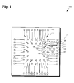
- FIG. 1 illustrates a top view of an exemplary structure in accordance with one embodiment of the present invention.
- FIG. 2 illustrates an expanded view of a portion of the exemplary structure in FIG. 1 according to an embodiment of the present invention.
- FIG. 3 illustrates a cross-sectional view of portion of a semiconductor die according to an embodiment of the present invention.
- the present invention is directed to controlled impedance transmission lines in a redistribution layer.
- the following description contains specific information pertaining to various embodiments and implementations of the invention.
- One skilled in the art will recognize that the present invention may be implemented in a manner different from that specifically discussed in the present application.
- some of the specific details of the invention are not discussed in order not to obscure the invention.
- the specific details not described in the present application are within the knowledge of a person of ordinary skills in the art.
- Semiconductor die 100 in FIG. 1 illustrates a top view of an exemplary semiconductor die in accordance with one embodiment of the present invention.
- a “semiconductor die,” such as semiconductor die 100 is also referred to as a “die,” a “chip,” or a “semiconductor chip” in the present application.
- BCB Benzocyclobutene
- transmission line refers to an “interconnect line” and the two terms are used interchangeably.
- FIG. 1 shows semiconductor die bond pad 102 , which is fabricated on the periphery of semiconductor die 100 .
- Semiconductor die bond pad 102 can be, for example, an input/output (“I/O”) pad interfacing with external devices.
- Semiconductor die bond pad 102 can comprise aluminum or other metals, such as copper, copper-aluminum alloy, or gold.
- FIG. 1 also shows transmission line 104 , which provides an electrical connection between semiconductor die bond pad 102 and solder bump 106 .
- transmission line 104 can be fabricated in a redistribution layer (“RDL”) on semiconductor die 100 .
- RDL redistribution layer
- transmission line 104 can be fabricated in an RDL utilizing a sputter deposition and etchback process.
- Transmission line 104 can comprise aluminum or other metals, such as copper, copper-aluminum alloy, or gold.
- solder bumps such as solder bump 106
- solder bump 106 allow semiconductor die 100 to be mounted on an interconnect substrate (not shown in FIG. 1) using flip chip technology.
- flip chip technology is a surface mount technology wherein the die is “flipped” over so that the active surface of the die faces an interconnect substrate.
- the electrical contact between the die and the interconnect substrate is achieved through an area array comprised of solder bumps, such as solder bump 106 , in FIG. 1.
- semiconductor die bond pads 108 , 110 , 112 , 114 , and 116 are fabricated on the periphery of semiconductor die 100 .
- Semiconductor die bond pads 108 , 110 , 112 , 114 , and 116 are similar to semiconductor die bond pad 102 discussed above, and comprise similar material as semiconductor die bond pad 102 . Further shown in FIG. 1, transmission lines 118 , 120 , 122 , 124 , and 126 , respectively, electrically connect semiconductor die bond pads 108 , 110 , 112 , 114 , and 116 to solder bumps 128 , 130 , 132 , 134 , and 136 . Transmission lines 118 , 120 , 122 , 124 , and 126 are fabricated in a similar manner as transmission line 104 described above.
- transmission lines 118 , 120 , 122 , 124 , and 126 comprise similar material as transmission line 104 .
- Transmission lines 118 , 120 , 122 , 124 , and 126 will be described in greater detail in relation to FIG. 2, and specifically with respect to the region enclosed by dashed line 138 (which corresponds to the region enclosed by dashed line 238 in FIG. 2).
- Each of the above transmission lines is driven by a respective I/O driver (not shown in FIG. 1) connected to an I/O pad, such as semiconductor die bond pad 108 .
- the I/O drivers may be coupled to the transmission lines directly and without going through semiconductor die bond pads.
- the impedance of a transmission line such as transmission line 104
- the signals transmitted from the I/O driver can traverse the transmission line in an optimal manner, i.e. at an optimal speed and with minimal energy loss.
- degradation of the quality of the signals outputted at the semiconductor die solder bumps, such as solder bump 106 can be minimized.
- an interconnect line i.e. a transmission line
- a reference ground line or plane also called “a ground return path”
- transmission line 118 is a ground line, i.e. a “ground return path.”
- transmission lines 126 and 122 have the same width and thickness.
- transmission line 122 is closer to transmission line 118 , the inductance per millimeter of length of transmission line 122 would be lower than the inductance per millimeter of length of transmission line 126 , which is further away from the ground line in this example, i.e. transmission line 118 . As such, if all other parameters are equal, the impedance of transmission line 126 would be greater than the impedance of transmission line 122 .
- the present invention provides a transmission line, such as transmission line 126 in FIG. 1, to meet a desired impedance, such as 50.0 ohms, by controlling the width and thickness of the transmission line and its distance is from a reference return ground path.
- a desired impedance such as 50.0 ohms
- FIG. 2 shows a top view of region 238 , which is an expanded view of region 138 in FIG. 1.
- semiconductor die bond pads 208 , 210 , 212 , 214 , and 216 , transmission lines 204 , 218 , 220 , 222 , 224 , and 226 , and solder bumps 206 , 228 , 230 , 232 , 234 , and 236 correspond to semiconductor die bond pads 108 , 110 , 112 , 114 , and 116 , transmission lines 104 , 118 , 120 , 122 , 124 , and 126 , and solder bumps 106 , 128 , 130 , 132 , 134 , and 136 in FIG. 1.
- width 240 refers to the width of transmission line 220 .
- width 240 might be 20.0 microns. If all other parameters remain unchanged, increasing the width of the transmission line generally results in a corresponding reduction in the impedance of the transmission line. For example, assuming that all other parameters remain unchanged, for a distance of 10.0 microns between transmission line 220 and a return ground path, increasing the value of width 240 from 20.0 microns to 35.0 microns results in a reduction in the impedance of transmission line 220 from 50.0 ohms to 35.0 ohms.
- line spacing 242 refers to the spacing between two transmission lines, such as transmission lines 224 and 226 , measured near the point where transmission lines 224 and 226 , respectively, connect to semiconductor die bond pads 214 and 216 .
- line spacing 242 might be 5.0 microns.
- pitch 244 refers to the distance between the centers of two adjacent solder balls, such as solder balls 234 and 236 .
- the value of pitch 244 might be 250.0 microns (it is noted that the distances in FIG. 2 are not drawn to scale).
- the resistance, capacitance, and inductance of a transmission line vary per millimeter of length.
- the resistance of a transmission line might be approximately 1.5 ohms per millimeter of length.
- the capacitance and inductance, respectively, of a transmission line might be approximately 0.13 to 0.15 picofarads (“pF”) and approximately 0.2 to 0.9 nano henries (“nH”) per millimeter of length.
- the above variation in the inductance of a transmission line per millimeter of length is extremely high because the inductance of the transmission line depends on the distance between the transmission line and a ground return path. For example, if the transmission line, such as transmission line 220 , is close to a ground return path, the inductance of the transmission line per millimeter of length will be close to the low end of the above inductance range, i.e. 0.2 nH. On the other hand, as the distance between the transmission line and the ground return path increases, the inductance of the transmission line per millimeter of length approaches the high end of the above inductance range, i.e. 0.9 nH.
- FIG. 3 shows a cross-sectional view of a semiconductor die in accordance with one embodiment of the present invention.
- FIG. 3 shows solder bump 302 planted on under bump metal (“UBM”) 304 .
- Solder bump 302 can provide an electrical connection between semiconductor die 300 and an interconnect substrate (not shown in FIG. 3).
- UBM 304 provides a surface for solder bump 302 to adhere to and also provides a low resistance electrical connection between solder bump 302 and transmission line 306 .
- UBM 304 is fabricated in a “redistribution process.” For example, UBM 304 may be fabricated on a redistribution layer using a sputter deposition process.
- UBM 304 can comprise a copper-chromium alloy. However, UBM 304 can comprise a stack of metals such as aluminum, nickel, vanadium, and copper.
- a “redistribution process” refers to a process whereby I/O pads on the periphery of a semiconductor die are re-routed to an area array configuration of solder bumps.
- the I/O pads are re-routed to the area array configuration by way of interconnect lines, i.e. transmission lines, fabricated in a redistribution layer.
- interconnect lines i.e. transmission lines
- the resulting area array configuration of solder bumps allows the semiconductor die to be connected to an interconnect substrate utilizing, for example, flip chip technology.
- FIG. 3 further shows transmission line 306 , which is situated on dielectric layer 308 .
- a first terminal of transmission line 306 is coupled to semiconductor die bond pad 313 by via 312
- a second terminal of transmission line 306 is coupled to UBM 304 .
- semiconductor die bond pad 313 may not be used.
- via 312 can directly couple transmission line 306 to interconnect metal line 311 , which in the present example is fabricated in metal level six.
- Transmission line 306 can be fabricated on the top surface of dielectric layer 308 by methods known to one of ordinary skill in the art. For example, transmission line 306 can be patterned on top surface of dielectric layer 308 utilizing a sputter deposition process.
- transmission line 306 can be patterned utilizing photoresist patterning with lift-off process.
- Transmission line 306 can comprise aluminum or other metals, such as copper, copper-aluminum alloy, or gold.
- Transmission line 306 and other transmission lines similarly fabricated on the top surface of dielectric layer 308 are part of the redistribution layer.
- Dielectric layer 308 can be deposited on a passivation layer, not shown in FIG. 3, on the top surface of semiconductor die 300 by methods well established in the art, such as by a spin on process.
- dielectric layer 308 can comprise a polymer dielectric such as BCB, which has a dielectric constant of approximately 3.0 to 3.5.
- the thickness of dielectric layer 308 can be approximately 5.0 to 10.0 microns.
- dielectric layer 308 can comprise silicon dioxide. In such instance, the thickness of dielectric layer 308 can be approximately 3.0 microns.
- dielectric layer 310 is situated over dielectric layer 308 .
- Dielectric layer 310 covers dielectric layer 308 and also covers the redistribution layer, including transmission lines such as transmission line 306 .
- Dielectric layer 310 is deposited on dielectric layer 308 by methods well known in the art.
- Dielectric layer 310 can comprise similar materials as dielectric layer 308 , such as BCB.
- Via 312 provides a connection between transmission line 306 and semiconductor die bond pad 313 in metal level six.
- Via 312 can be formed in dielectric layer 308 by utilizing a photolithographic process or by other methods known to a person of ordinary skill in the art.
- metal level six is the last metal level in semiconductor die 300 .
- the last metal level in the semiconductor die may be a metal level other than metal level six.
- solder bump 314 is planted on UBM 316 . Similar to solder bump 302 described above, solder bump 314 can also provide an electrical connection between semiconductor die 300 and an interconnect substrate (not shown in FIG. 3). UBM 316 provides a surface for solder bump 314 to adhere to and also provides a low resistance electrical connection between solder bump 314 and transmission line 318 . UBM 316 comprises similar material as UBM 304 described above, and is also fabricated in a similar manner as UBM 304 .
- FIG. 3 further shows transmission line 318 , which is situated on dielectric layer 308 .
- a first terminal of transmission line 318 is coupled to semiconductor die bond pad 321 by via 320
- a second terminal of transmission line 318 is coupled to UBM 316 .
- Transmission line 318 comprises similar material as transmission line 306 described above, and is also fabricated in a similar manner as transmission line 306 .
- Via 320 provides a connection between transmission line 318 and semiconductor die bond pad 321 in metal level six.
- Via 320 is formed in dielectric layer 308 in a similar manner as via 312 described above.
- Semiconductor die bond pad 321 is coupled to interconnect metal line 315 , which, in the present example, is fabricated in metal level six.
- distance 322 refers to the distance between ground return path 324 in metal level six and transmission line 306 . Since dielectric laster 308 is situated between metal level six and transmission line 306 , distance 322 also refers to the thickness of dielectric layer 308 . In one exemplary embodiment, distance 322 can be approximately 5.0 to 10.0 microns. Further shown in FIG. 3, via 326 provides a connection between ground return path 324 in metal level six and ground line 328 , which is in metal level five. In another embodiment, ground return paths of the invention's transmission lines may be in the RDL. In such instance, the ground return path would be in the same “plane” as the invention's transmission lines.
- dielectric layer 330 refers to a dielectric layer between metal level 6 and metal level 5 in semiconductor die 300 .
- Dielectric layer 330 can comprise a dielectric such as silicon dioxide.
- distance 332 refers to the distance between ground return path 328 in metal level five and transmission line 318 .
- the impedance of transmission line 306 is affected by distance 322 , i.e. the distance between transmission line 306 and ground return path 324 in metal level six.
- distance 322 i.e. the distance between transmission line 306 and ground return path 324 in metal level six.
- the impedance transmission line 306 can be approximately 50.0 ohms.
- the impedance of transmission line 306 will become greater than 50.0 ohms.
- the impedance of transmission line 306 can be increased or decreased by increasing or decreasing distance 322 .
- distance 322 can be increased by increasing the thickness of dielectric layer 308 , which effectively increases the distance, i.e. the separation, between transmission line 306 and return ground path 324 .
- Distance 322 can also be increased by utilizing a return ground path in a lower metal level in semiconductor die 300 , such as metal level five.
- transmission line 318 utilizes return ground path 328 , which is in metal level five.
- distance 332 i.e. the distance between transmission line 318 and return ground path 328 in metal level five, is greater than distance 322 , i.e. the distance between transmission line 306 and return ground path 324 in metal level six. Accordingly, for the same line width and line thickness and assuming that all other parameters are unchanged, transmission line 318 will have a higher impedance than transmission line 306 .
- the impedances of various transmission lines are controlled not only by using conventional impedance control techniques, such as controlling the width and thickness of the transmission lines, but also by designing for a particular distance between each transmission line and a ground return path situated therebelow in the semiconductor die.
- the design and control of the distance between transmission lines and the ground return paths below them is made possible by using the RDL to fabricate the transmission lines and also by designing the distance of each transmission line from an underlying ground return path in a manner so as to result in a desired impedance, such as a 50.0 ohm impedance.
- the invention results in an additional control over the impedance of the transmission line, beyond the conventional control over the impedance which consisted of controlling parameters such as width and thickness of the transmission line. For example, by selecting metal level five to serve as a ground return path for one transmission line, metal level six to serve as a ground return path for another transmission line, and metal level four to serve as a ground return path for yet another transmission line, the impedances of various transmission lines fabricated in the RDL are fine tuned and optimized.
- FIG. 3 illustrated that by choosing metal level six to serve as the ground return path for transmission line 306 , the impedance of transmission line 306 was reduced relative to the impedance of transmission line 318 which utilized metal level five as its ground return path.
- the invention results in a clever design of ground return paths within the semiconductor die and takes into account the RDL transmission lines that are situated above the ground lines of the semiconductor die.
- the distance between ground lines existing in various metal levels and any transmission lines driven by or coupled to I/O drivers of the semiconductor die would not be taken into account, and the invention's valuable control over the impedance of RDL transmission lines did not exist.
- the proper distribution of ground lines under the transmission lines fabricated in the RDL takes place, for example, by appropriate layout considerations which in turn result in a proper distribution of ground lines at desired “depths,” i.e.
- the present invention results in transmission lines that reduce manufacturing costs by reducing the required number and strength of I/O drivers driving the transmission lines.
Landscapes
- Semiconductor Integrated Circuits (AREA)
- Design And Manufacture Of Integrated Circuits (AREA)
- Waveguides (AREA)
- Control Of Motors That Do Not Use Commutators (AREA)
- Communication Cables (AREA)
Abstract
Description
- 1. Field of the Invention
- The present invention is generally in the field of semiconductor circuits. More specifically, the present invention is in the field of transmission line impedance control in semiconductor circuits.
- 2. Background Art
- Consumer demand for smaller, more complex, and faster devices operating at high frequencies, such as wireless communications devices and Bluetooth RF transceivers, has resulted in an increased demand for semiconductor dies with higher densities. As the density of the semiconductor die increases, the number of input/output (“I/O”) pads on the periphery of the semiconductor die also increases. As a result, there is a diminishing amount of space on the periphery of the semiconductor die in which to place the I/O pads. To solve this problem, semiconductor manufacturers are moving to area array I/O designs.
- In an area array I/O design, I/O pads on the periphery of the semiconductor die are relocated to an area array in the center of the semiconductor die using a redistribution layer (“RDL”). Typically, the RDL is a thin film routing layer formed primarily from aluminum or copper. The RDL comprises interconnect lines, also referred to as transmission lines in the present application, that provide electrical connections between I/O pads on the periphery of the semiconductor die and solder bumps in an area array configuration. Under bump metal (“UBM”) is used to attach the solder bumps to the interconnect lines.
- The interconnect lines, i.e. the transmission lines, in the RDL are driven by I/O drivers (or “line drivers”) located near the I/O pads in the semiconductor die. The I/O drivers expect to interface with transmission lines having a certain impedance. If the impedance of a transmission line does not match the impedance of its respective I/O driver, the transmission of electrical signals through the transmission line will not occur in an optimized manner and will be generally slowed down.
- One approach used to reduce the impact of this impedance mismatch problem has been to increase the strength of the I/O driver. However, utilization of substantially stronger I/O drivers will increase the cost of manufacturing the semiconductor die. Another approach used to address the problem has been to increase the number of I/O drivers that drive the transmission line. However, increasing the number of I/O drivers also increases the cost of manufacturing the semiconductor die.
- Thus, there is a need in the art for a transmission line in an RDL that can match a required impedance of an I/O driver in a semiconductor die.
- The present invention is directed to controlled impedance transmission lines in a redistribution layer. The invention overcomes the need in the art for transmission lines in a redistribution layer that can match required impedances of I/O drivers in a semiconductor die.
- In one embodiment, the invention includes first and second transmission lines fabricated in a redistribution layer over a semiconductor die. The first transmission line has a first distance from a first ground return path formed in a first metal level. For example, the first ground return path might be formed in metal level six within the semiconductor die. The first transmission line has a first impedance corresponding to the first distance. In other words, the impedance of the first transmission line is affected by the distance between the first transmission line and the first ground return path, which in this example is the distance between the first transmission line and the ground return path formed in metal level six.
- Similar to the first transmission line, the second transmission line has a second distance from a second ground return path formed in a second metal level. For example, the second ground return path might be formed in metal level five within the semiconductor die. The second transmission line has a second impedance corresponding to the second distance. In other words, the impedance of the second transmission line is affected by the distance between the second transmission line and the second ground return path, which in this example is the distance between the second transmission line and the ground return path formed in metal level five.
- Thus, by determining which particular metal level in the semiconductor die should serve as a ground return path for a particular transmission line, the invention results in an additional control over the impedance of transmission lines, beyond the conventional control over the impedance which consisted of controlling parameters such as width and thickness of the transmission lines.
- Various other concepts, features, and advantages of the present invention are discussed in the following sections of the present application.
- FIG. 1 illustrates a top view of an exemplary structure in accordance with one embodiment of the present invention.
- FIG. 2 illustrates an expanded view of a portion of the exemplary structure in FIG. 1 according to an embodiment of the present invention.
- FIG. 3 illustrates a cross-sectional view of portion of a semiconductor die according to an embodiment of the present invention.
- The present invention is directed to controlled impedance transmission lines in a redistribution layer. The following description contains specific information pertaining to various embodiments and implementations of the invention. One skilled in the art will recognize that the present invention may be implemented in a manner different from that specifically discussed in the present application. Moreover, some of the specific details of the invention are not discussed in order not to obscure the invention. The specific details not described in the present application are within the knowledge of a person of ordinary skills in the art.
- The drawings in the present application and their accompanying detailed description are directed to merely example embodiments of the invention. To maintain brevity, other embodiments of the invention that use the principles of the present invention are not specifically described in the present application and are not specifically illustrated by the present drawings.
- Semiconductor die 100 in FIG. 1 illustrates a top view of an exemplary semiconductor die in accordance with one embodiment of the present invention. It is noted that a “semiconductor die,” such as
semiconductor die 100, is also referred to as a “die,” a “chip,” or a “semiconductor chip” in the present application. Those skilled in the art will appreciate that various elements and features are not shown in FIG. 1 to avoid obscuring the invention and to facilitate the description of FIG. 1. For example, a layer of dielectric, such as Benzocyclobutene (“BCB”), that is typically deposited over transmission lines, such astransmission line 104, is not shown in FIG. 1 to allow the transmission lines to be viewed. It will be shown in relation to FIG. 1, and further in relation to FIGS. 2 and 3, that the impedance of an exemplary embodiment of the present invention's transmission line can be controlled to match a desired impedance, such as an industry standard impedance of 50.0 ohm. Also, it is noted that, in the present application, the term “transmission line” refers to an “interconnect line” and the two terms are used interchangeably. - FIG. 1 shows semiconductor die
bond pad 102, which is fabricated on the periphery of semiconductor die 100. Semiconductordie bond pad 102 can be, for example, an input/output (“I/O”) pad interfacing with external devices. Semiconductordie bond pad 102 can comprise aluminum or other metals, such as copper, copper-aluminum alloy, or gold. FIG. 1 also showstransmission line 104, which provides an electrical connection between semiconductordie bond pad 102 andsolder bump 106. According to an embodiment of the present invention,transmission line 104 can be fabricated in a redistribution layer (“RDL”) onsemiconductor die 100. For example,transmission line 104 can be fabricated in an RDL utilizing a sputter deposition and etchback process.Transmission line 104 can comprise aluminum or other metals, such as copper, copper-aluminum alloy, or gold. - By way of background, solder bumps, such as
solder bump 106, allow semiconductor die 100 to be mounted on an interconnect substrate (not shown in FIG. 1) using flip chip technology. As is known in the art, flip chip technology is a surface mount technology wherein the die is “flipped” over so that the active surface of the die faces an interconnect substrate. In flip chip technology, the electrical contact between the die and the interconnect substrate is achieved through an area array comprised of solder bumps, such assolder bump 106, in FIG. 1. Also shown in FIG. 1, semiconductor diebond pads bond pads bond pad 102 discussed above, and comprise similar material as semiconductor diebond pad 102. Further shown in FIG. 1,transmission lines bond pads bumps Transmission lines transmission line 104 described above. Also,transmission lines transmission line 104.Transmission lines line 238 in FIG. 2). - Each of the above transmission lines, such as
transmission line 118, is driven by a respective I/O driver (not shown in FIG. 1) connected to an I/O pad, such as semiconductor diebond pad 108. In another embodiment, the I/O drivers may be coupled to the transmission lines directly and without going through semiconductor die bond pads. When the impedance of a transmission line, such astransmission line 104, closely matches the impedance of its respective I/O driver, the signals transmitted from the I/O driver can traverse the transmission line in an optimal manner, i.e. at an optimal speed and with minimal energy loss. As a result, degradation of the quality of the signals outputted at the semiconductor die solder bumps, such assolder bump 106, can be minimized. - The width and thickness of an interconnect line (i.e. a transmission line) and the distance of the interconnect line from a reference ground line or plane, also called “a ground return path,” affects the resistance, inductance and capacitance, and thus the total impedance, of the interconnect line. For example, assume that
transmission line 118 is a ground line, i.e. a “ground return path.” Further assume thattransmission lines transmission line 122 is closer totransmission line 118, the inductance per millimeter of length oftransmission line 122 would be lower than the inductance per millimeter of length oftransmission line 126, which is further away from the ground line in this example, i.e.transmission line 118. As such, if all other parameters are equal, the impedance oftransmission line 126 would be greater than the impedance oftransmission line 122. - Thus, as will be shown below, the present invention provides a transmission line, such as
transmission line 126 in FIG. 1, to meet a desired impedance, such as 50.0 ohms, by controlling the width and thickness of the transmission line and its distance is from a reference return ground path. - FIG. 2 shows a top view of
region 238, which is an expanded view ofregion 138 in FIG. 1. In particular, semiconductor diebond pads transmission lines solder bumps bond pads transmission lines solder bumps - Also shown in FIG. 2,
width 240 refers to the width oftransmission line 220. As an example,width 240 might be 20.0 microns. If all other parameters remain unchanged, increasing the width of the transmission line generally results in a corresponding reduction in the impedance of the transmission line. For example, assuming that all other parameters remain unchanged, for a distance of 10.0 microns betweentransmission line 220 and a return ground path, increasing the value ofwidth 240 from 20.0 microns to 35.0 microns results in a reduction in the impedance oftransmission line 220 from 50.0 ohms to 35.0 ohms. - Further shown in FIG. 2,
line spacing 242 refers to the spacing between two transmission lines, such astransmission lines transmission lines bond pads line spacing 242 might be 5.0 microns. Also shown in FIG. 2,pitch 244 refers to the distance between the centers of two adjacent solder balls, such assolder balls pitch 244 might be 250.0 microns (it is noted that the distances in FIG. 2 are not drawn to scale). - For given values of line width and line spacing, the resistance, capacitance, and inductance of a transmission line, such as
transmission line 220, vary per millimeter of length. For example, for a line width equal to 20.0 microns and a line spacing equal to 5.0 microns, the resistance of a transmission line might be approximately 1.5 ohms per millimeter of length. Also, using the above values for line width and line spacing, the capacitance and inductance, respectively, of a transmission line might be approximately 0.13 to 0.15 picofarads (“pF”) and approximately 0.2 to 0.9 nano henries (“nH”) per millimeter of length. - The above variation in the inductance of a transmission line per millimeter of length, i.e. 0.2 to 0.9 nH, is extremely high because the inductance of the transmission line depends on the distance between the transmission line and a ground return path. For example, if the transmission line, such as
transmission line 220, is close to a ground return path, the inductance of the transmission line per millimeter of length will be close to the low end of the above inductance range, i.e. 0.2 nH. On the other hand, as the distance between the transmission line and the ground return path increases, the inductance of the transmission line per millimeter of length approaches the high end of the above inductance range, i.e. 0.9 nH. - As discussed below, critical parameters, such as the distance between a transmission line and a ground return path, are properly controlled by use of the invention's techniques described below in order for the transmission line to achieve and match a desired impedance. The control of various parameters, and in particular the distance between a transmission line and a ground return path, according to the present invention, will be further discussed below in relation to FIG. 3.
- FIG. 3 shows a cross-sectional view of a semiconductor die in accordance with one embodiment of the present invention. FIG. 3 shows
solder bump 302 planted on under bump metal (“UBM”) 304.Solder bump 302 can provide an electrical connection between semiconductor die 300 and an interconnect substrate (not shown in FIG. 3).UBM 304 provides a surface forsolder bump 302 to adhere to and also provides a low resistance electrical connection betweensolder bump 302 andtransmission line 306.UBM 304 is fabricated in a “redistribution process.” For example,UBM 304 may be fabricated on a redistribution layer using a sputter deposition process.UBM 304 can comprise a copper-chromium alloy. However,UBM 304 can comprise a stack of metals such as aluminum, nickel, vanadium, and copper. - By way of background, a “redistribution process” refers to a process whereby I/O pads on the periphery of a semiconductor die are re-routed to an area array configuration of solder bumps. The I/O pads are re-routed to the area array configuration by way of interconnect lines, i.e. transmission lines, fabricated in a redistribution layer. The resulting area array configuration of solder bumps allows the semiconductor die to be connected to an interconnect substrate utilizing, for example, flip chip technology.
- FIG. 3 further shows
transmission line 306, which is situated ondielectric layer 308. A first terminal oftransmission line 306 is coupled to semiconductor diebond pad 313 by via 312, and a second terminal oftransmission line 306 is coupled toUBM 304. In another embodiment, semiconductor diebond pad 313 may not be used. In such instance, via 312 can directly coupletransmission line 306 to interconnectmetal line 311, which in the present example is fabricated in metal level six.Transmission line 306 can be fabricated on the top surface ofdielectric layer 308 by methods known to one of ordinary skill in the art. For example,transmission line 306 can be patterned on top surface ofdielectric layer 308 utilizing a sputter deposition process. By way of further example,transmission line 306 can be patterned utilizing photoresist patterning with lift-off process.Transmission line 306 can comprise aluminum or other metals, such as copper, copper-aluminum alloy, or gold.Transmission line 306 and other transmission lines similarly fabricated on the top surface ofdielectric layer 308 are part of the redistribution layer. -
Dielectric layer 308 can be deposited on a passivation layer, not shown in FIG. 3, on the top surface of semiconductor die 300 by methods well established in the art, such as by a spin on process. In the present embodiment,dielectric layer 308 can comprise a polymer dielectric such as BCB, which has a dielectric constant of approximately 3.0 to 3.5. The thickness ofdielectric layer 308 can be approximately 5.0 to 10.0 microns. In another embodiment,dielectric layer 308 can comprise silicon dioxide. In such instance, the thickness ofdielectric layer 308 can be approximately 3.0 microns. - Also shown in FIG. 3,
dielectric layer 310 is situated overdielectric layer 308.Dielectric layer 310 coversdielectric layer 308 and also covers the redistribution layer, including transmission lines such astransmission line 306.Dielectric layer 310 is deposited ondielectric layer 308 by methods well known in the art.Dielectric layer 310 can comprise similar materials asdielectric layer 308, such as BCB. - Via 312 provides a connection between
transmission line 306 and semiconductor diebond pad 313 in metal level six. Via 312 can be formed indielectric layer 308 by utilizing a photolithographic process or by other methods known to a person of ordinary skill in the art. In the present example, metal level six is the last metal level in semiconductor die 300. In other embodiments, the last metal level in the semiconductor die may be a metal level other than metal level six. - Also shown in FIG. 3,
solder bump 314 is planted onUBM 316. Similar tosolder bump 302 described above,solder bump 314 can also provide an electrical connection between semiconductor die 300 and an interconnect substrate (not shown in FIG. 3).UBM 316 provides a surface forsolder bump 314 to adhere to and also provides a low resistance electrical connection betweensolder bump 314 and transmission line 318.UBM 316 comprises similar material asUBM 304 described above, and is also fabricated in a similar manner asUBM 304. - FIG. 3 further shows transmission line 318, which is situated on
dielectric layer 308. A first terminal of transmission line 318 is coupled to semiconductor diebond pad 321 by via 320, and a second terminal of transmission line 318 is coupled toUBM 316. Transmission line 318 comprises similar material astransmission line 306 described above, and is also fabricated in a similar manner astransmission line 306. Via 320 provides a connection between transmission line 318 and semiconductor diebond pad 321 in metal level six. Via 320 is formed indielectric layer 308 in a similar manner as via 312 described above. Semiconductor diebond pad 321 is coupled to interconnectmetal line 315, which, in the present example, is fabricated in metal level six. - Also shown in FIG. 3,
distance 322 refers to the distance betweenground return path 324 in metal level six andtransmission line 306. Sincedielectric laster 308 is situated between metal level six andtransmission line 306,distance 322 also refers to the thickness ofdielectric layer 308. In one exemplary embodiment,distance 322 can be approximately 5.0 to 10.0 microns. Further shown in FIG. 3, via 326 provides a connection betweenground return path 324 in metal level six andground line 328, which is in metal level five. In another embodiment, ground return paths of the invention's transmission lines may be in the RDL. In such instance, the ground return path would be in the same “plane” as the invention's transmission lines. - Also shown in FIG. 3,
dielectric layer 330 refers to a dielectric layer between metal level 6 and metal level 5 in semiconductor die 300.Dielectric layer 330 can comprise a dielectric such as silicon dioxide. Further shown in FIG. 3,distance 332 refers to the distance betweenground return path 328 in metal level five and transmission line 318. - The impedance of
transmission line 306 is affected bydistance 322, i.e. the distance betweentransmission line 306 andground return path 324 in metal level six. For example, whendistance 322 is equal to 20.0 microns and for a line width of 40.0 microns fortransmission line 306, theimpedance transmission line 306 can be approximately 50.0 ohms. However, by increasingdistance 322, the impedance oftransmission line 306 will become greater than 50.0 ohms. - For a given line width and thickness, the impedance of
transmission line 306 can be increased or decreased by increasing or decreasingdistance 322. For example,distance 322 can be increased by increasing the thickness ofdielectric layer 308, which effectively increases the distance, i.e. the separation, betweentransmission line 306 and returnground path 324. Distance 322 can also be increased by utilizing a return ground path in a lower metal level in semiconductor die 300, such as metal level five. For example, transmission line 318 utilizesreturn ground path 328, which is in metal level five. Thus,distance 332, i.e. the distance between transmission line 318 and returnground path 328 in metal level five, is greater thandistance 322, i.e. the distance betweentransmission line 306 and returnground path 324 in metal level six. Accordingly, for the same line width and line thickness and assuming that all other parameters are unchanged, transmission line 318 will have a higher impedance thantransmission line 306. - According to the present invention, the impedances of various transmission lines, such as
transmission lines 306 and 318 in FIG. 3, are controlled not only by using conventional impedance control techniques, such as controlling the width and thickness of the transmission lines, but also by designing for a particular distance between each transmission line and a ground return path situated therebelow in the semiconductor die. The design and control of the distance between transmission lines and the ground return paths below them is made possible by using the RDL to fabricate the transmission lines and also by designing the distance of each transmission line from an underlying ground return path in a manner so as to result in a desired impedance, such as a 50.0 ohm impedance. - In other words, by determining which particular metal level in the semiconductor die should serve as a ground return path for a particular transmission line, the invention results in an additional control over the impedance of the transmission line, beyond the conventional control over the impedance which consisted of controlling parameters such as width and thickness of the transmission line. For example, by selecting metal level five to serve as a ground return path for one transmission line, metal level six to serve as a ground return path for another transmission line, and metal level four to serve as a ground return path for yet another transmission line, the impedances of various transmission lines fabricated in the RDL are fine tuned and optimized. By way of a specific example, FIG. 3 illustrated that by choosing metal level six to serve as the ground return path for
transmission line 306, the impedance oftransmission line 306 was reduced relative to the impedance of transmission line 318 which utilized metal level five as its ground return path. - As such, the invention results in a clever design of ground return paths within the semiconductor die and takes into account the RDL transmission lines that are situated above the ground lines of the semiconductor die. In contrast, in conventional techniques, the distance between ground lines existing in various metal levels and any transmission lines driven by or coupled to I/O drivers of the semiconductor die would not be taken into account, and the invention's valuable control over the impedance of RDL transmission lines did not exist. The proper distribution of ground lines under the transmission lines fabricated in the RDL takes place, for example, by appropriate layout considerations which in turn result in a proper distribution of ground lines at desired “depths,” i.e. at desired metal levels, so as to result in a precise impedance, for example a 50.0 ohm impedance, for a given transmission line connected to a particular I/O driver. As one of its benefits, the present invention results in transmission lines that reduce manufacturing costs by reducing the required number and strength of I/O drivers driving the transmission lines.
- From the above description of the invention it is manifest that various techniques can be used for implementing the concepts of the present invention without departing from its scope. Moreover, while the invention has been described with specific reference to certain embodiments, a person of ordinary skill in the art would recognize that changes can be made in form and detail without departing from the spirit and the scope of the invention. The described embodiments are to be considered in all respects as illustrative and not restrictive. It should also be understood that the invention is not limited to the particular embodiments described herein, but is capable of many rearrangements, modifications, and substitutions without departing from the scope of the invention.
- Thus, controlled impedance transmission lines in a redistribution layer have been described.
Claims (23)
Priority Applications (7)
| Application Number | Priority Date | Filing Date | Title |
|---|---|---|---|
| US10/012,812 US6674174B2 (en) | 2001-11-13 | 2001-11-13 | Controlled impedance transmission lines in a redistribution layer |
| EP02780619A EP1444731B1 (en) | 2001-11-13 | 2002-11-12 | Controlled impedance transmission lines in a redistribution layer |
| CNB028221672A CN100336213C (en) | 2001-11-13 | 2002-11-12 | Controlled Impedance Transmission Lines in the Redistribution Layer |
| AT02780619T ATE508474T1 (en) | 2001-11-13 | 2002-11-12 | TRANSMISSION LINES WITH ADJUSTABLE IMPEDANCE IN A DISTRIBUTION LAYER |
| DE60239950T DE60239950D1 (en) | 2001-11-13 | 2002-11-12 | TRANSMISSION LINES WITH ADJUSTABLE IMPEDANCE IN A DISTRIBUTION LAYER |
| KR10-2004-7005462A KR100534048B1 (en) | 2001-11-13 | 2002-11-12 | Controlled impedance transmission lines in a redistribution layer |
| PCT/US2002/036207 WO2003043083A1 (en) | 2001-11-13 | 2002-11-12 | Controlled impedance transmission lines in a redistribution layer |
Applications Claiming Priority (1)
| Application Number | Priority Date | Filing Date | Title |
|---|---|---|---|
| US10/012,812 US6674174B2 (en) | 2001-11-13 | 2001-11-13 | Controlled impedance transmission lines in a redistribution layer |
Publications (2)
| Publication Number | Publication Date |
|---|---|
| US20030193078A1 true US20030193078A1 (en) | 2003-10-16 |
| US6674174B2 US6674174B2 (en) | 2004-01-06 |
Family
ID=21756804
Family Applications (1)
| Application Number | Title | Priority Date | Filing Date |
|---|---|---|---|
| US10/012,812 Expired - Lifetime US6674174B2 (en) | 2001-11-13 | 2001-11-13 | Controlled impedance transmission lines in a redistribution layer |
Country Status (7)
| Country | Link |
|---|---|
| US (1) | US6674174B2 (en) |
| EP (1) | EP1444731B1 (en) |
| KR (1) | KR100534048B1 (en) |
| CN (1) | CN100336213C (en) |
| AT (1) | ATE508474T1 (en) |
| DE (1) | DE60239950D1 (en) |
| WO (1) | WO2003043083A1 (en) |
Cited By (3)
| Publication number | Priority date | Publication date | Assignee | Title |
|---|---|---|---|---|
| US6822327B1 (en) * | 2003-06-13 | 2004-11-23 | Delphi Technologies, Inc. | Flip-chip interconnected with increased current-carrying capability |
| US7098518B1 (en) * | 2003-08-27 | 2006-08-29 | National Semiconductor Corporation | Die-level opto-electronic device and method of making same |
| US20140211438A1 (en) * | 2013-01-25 | 2014-07-31 | Taiwan Semiconductor Manufacturing Company, Ltd. | Methods and Apparatus for Transmission Lines in Packages |
Families Citing this family (15)
| Publication number | Priority date | Publication date | Assignee | Title |
|---|---|---|---|---|
| US7342312B2 (en) * | 2004-09-29 | 2008-03-11 | Rohm Co., Ltd. | Semiconductor device |
| DE102005002707B4 (en) * | 2005-01-19 | 2007-07-26 | Infineon Technologies Ag | Method for producing electrical connections in a semiconductor device by means of coaxial microconnection elements |
| US7541251B2 (en) * | 2006-02-10 | 2009-06-02 | California Micro Devices | Wire bond and redistribution layer process |
| US8946873B2 (en) * | 2007-08-28 | 2015-02-03 | Micron Technology, Inc. | Redistribution structures for microfeature workpieces |
| US8193878B2 (en) * | 2008-06-24 | 2012-06-05 | International Business Machines Corporation | Structure, structure and method for providing an on-chip variable delay transmission line with fixed characteristic impedance |
| KR20110031277A (en) * | 2008-06-24 | 2011-03-25 | 인터내셔널 비지네스 머신즈 코포레이션 | Design structures, structures and methods for providing on-chip variable delayed transmission lines with fixed characteristic impedance |
| US8138857B2 (en) * | 2008-06-24 | 2012-03-20 | International Business Machines Corporation | Structure, structure and method for providing an on-chip variable delay transmission line with fixed characteristic impedance |
| WO2010007782A1 (en) * | 2008-07-15 | 2010-01-21 | パナソニック株式会社 | Slow wave transmission line |
| US8659170B2 (en) * | 2010-01-20 | 2014-02-25 | Taiwan Semiconductor Manufacturing Company, Ltd. | Semiconductor device having conductive pads and a method of manufacturing the same |
| KR101685057B1 (en) * | 2010-01-22 | 2016-12-09 | 삼성전자주식회사 | Stacked package of semiconductor device |
| KR101666192B1 (en) | 2010-02-02 | 2016-10-14 | 삼성전자 주식회사 | Semiconductor chip and semiconductor module having the same |
| CN102469679A (en) * | 2010-11-05 | 2012-05-23 | 富士康(昆山)电脑接插件有限公司 | Printed circuit board |
| US9711471B2 (en) | 2015-11-18 | 2017-07-18 | Nxp Usa, Inc. | Semiconductor device package, electronic device and method of manufacturing electronic devices using wafer level chip scale package technology |
| JP6798252B2 (en) * | 2016-10-31 | 2020-12-09 | 住友電気工業株式会社 | High frequency device |
| KR20220019331A (en) | 2020-08-10 | 2022-02-17 | 삼성전자주식회사 | Package substrate and semiconductor package including the same |
Family Cites Families (20)
| Publication number | Priority date | Publication date | Assignee | Title |
|---|---|---|---|---|
| US4498122A (en) * | 1982-12-29 | 1985-02-05 | At&T Bell Laboratories | High-speed, high pin-out LSI chip package |
| JP2833996B2 (en) * | 1994-05-25 | 1998-12-09 | 日本電気株式会社 | Flexible film and semiconductor device having the same |
| JP3142723B2 (en) * | 1994-09-21 | 2001-03-07 | シャープ株式会社 | Semiconductor device and manufacturing method thereof |
| JP2546192B2 (en) * | 1994-09-30 | 1996-10-23 | 日本電気株式会社 | Film carrier semiconductor device |
| KR100218996B1 (en) * | 1995-03-24 | 1999-09-01 | 모기 쥰이찌 | Semiconductor device |
| US6072236A (en) * | 1996-03-07 | 2000-06-06 | Micron Technology, Inc. | Micromachined chip scale package |
| US6169329B1 (en) * | 1996-04-02 | 2001-01-02 | Micron Technology, Inc. | Semiconductor devices having interconnections using standardized bonding locations and methods of designing |
| WO1998018161A1 (en) * | 1996-10-17 | 1998-04-30 | Seiko Epson Corporation | Semiconductor device, method of its manufacture, circuit substrate, and film carrier tape |
| JP2982738B2 (en) * | 1997-04-04 | 1999-11-29 | 日本電気株式会社 | Structure of ceramic chip size package |
| JP3335575B2 (en) * | 1997-06-06 | 2002-10-21 | 松下電器産業株式会社 | Semiconductor device and manufacturing method thereof |
| JP3152180B2 (en) * | 1997-10-03 | 2001-04-03 | 日本電気株式会社 | Semiconductor device and manufacturing method thereof |
| US6025647A (en) | 1997-11-24 | 2000-02-15 | Vlsi Technology, Inc. | Apparatus for equalizing signal parameters in flip chip redistribution layers |
| US6248429B1 (en) * | 1998-07-06 | 2001-06-19 | Micron Technology, Inc. | Metallized recess in a substrate |
| US5994766A (en) * | 1998-09-21 | 1999-11-30 | Vlsi Technology, Inc. | Flip chip circuit arrangement with redistribution layer that minimizes crosstalk |
| JP2000138313A (en) * | 1998-10-30 | 2000-05-16 | Shinko Electric Ind Co Ltd | Semiconductor device and manufacturing method thereof |
| US6078100A (en) * | 1999-01-13 | 2000-06-20 | Micron Technology, Inc. | Utilization of die repattern layers for die internal connections |
| US6407450B1 (en) * | 1999-07-15 | 2002-06-18 | Altera Corporation | Semiconductor package with universal substrate for electrically interfacing with different sized chips that have different logic functions |
| US6249047B1 (en) * | 1999-09-02 | 2001-06-19 | Micron Technology, Inc. | Ball array layout |
| JP4301661B2 (en) * | 1999-11-12 | 2009-07-22 | 富士通マイクロエレクトロニクス株式会社 | Contact film and device mounting structure used for ball grid array device |
| JP3578964B2 (en) * | 2000-03-21 | 2004-10-20 | 富士通株式会社 | Semiconductor device and manufacturing method thereof |
-
2001
- 2001-11-13 US US10/012,812 patent/US6674174B2/en not_active Expired - Lifetime
-
2002
- 2002-11-12 EP EP02780619A patent/EP1444731B1/en not_active Expired - Lifetime
- 2002-11-12 CN CNB028221672A patent/CN100336213C/en not_active Expired - Lifetime
- 2002-11-12 AT AT02780619T patent/ATE508474T1/en not_active IP Right Cessation
- 2002-11-12 DE DE60239950T patent/DE60239950D1/en not_active Expired - Lifetime
- 2002-11-12 KR KR10-2004-7005462A patent/KR100534048B1/en not_active Expired - Lifetime
- 2002-11-12 WO PCT/US2002/036207 patent/WO2003043083A1/en not_active Ceased
Cited By (9)
| Publication number | Priority date | Publication date | Assignee | Title |
|---|---|---|---|---|
| US6822327B1 (en) * | 2003-06-13 | 2004-11-23 | Delphi Technologies, Inc. | Flip-chip interconnected with increased current-carrying capability |
| US20040251542A1 (en) * | 2003-06-13 | 2004-12-16 | Pankaj Mithal | Flip-chip interconnect with increased current-carrying capability |
| US7098518B1 (en) * | 2003-08-27 | 2006-08-29 | National Semiconductor Corporation | Die-level opto-electronic device and method of making same |
| US7468288B1 (en) | 2003-08-27 | 2008-12-23 | National Semiconductor Corporation | Die-level opto-electronic device and method of making same |
| US20140211438A1 (en) * | 2013-01-25 | 2014-07-31 | Taiwan Semiconductor Manufacturing Company, Ltd. | Methods and Apparatus for Transmission Lines in Packages |
| US9171798B2 (en) * | 2013-01-25 | 2015-10-27 | Taiwan Semiconductor Manufacturing Company, Ltd. | Methods and apparatus for transmission lines in packages |
| US10269746B2 (en) | 2013-01-25 | 2019-04-23 | Taiwan Semiconductor Manufacturing Company, Ltd. | Methods and apparatus for transmission lines in packages |
| US10840201B2 (en) | 2013-01-25 | 2020-11-17 | Taiwan Semiconductor Manufacturing Company, Ltd. | Methods and apparatus for transmission lines in packages |
| US11978712B2 (en) | 2013-01-25 | 2024-05-07 | Taiwan Semiconductor Manufacturing Company, Ltd. | Method of forming semiconductor package transmission lines with micro-bump lines |
Also Published As
| Publication number | Publication date |
|---|---|
| KR100534048B1 (en) | 2005-12-06 |
| DE60239950D1 (en) | 2011-06-16 |
| EP1444731A1 (en) | 2004-08-11 |
| KR20050044326A (en) | 2005-05-12 |
| US6674174B2 (en) | 2004-01-06 |
| EP1444731B1 (en) | 2011-05-04 |
| EP1444731A4 (en) | 2005-04-06 |
| CN1599957A (en) | 2005-03-23 |
| ATE508474T1 (en) | 2011-05-15 |
| CN100336213C (en) | 2007-09-05 |
| WO2003043083A1 (en) | 2003-05-22 |
Similar Documents
| Publication | Publication Date | Title |
|---|---|---|
| US6674174B2 (en) | Controlled impedance transmission lines in a redistribution layer | |
| US6869870B2 (en) | High performance system-on-chip discrete components using post passivation process | |
| US7531417B2 (en) | High performance system-on-chip passive device using post passivation process | |
| US7592703B2 (en) | RF and MMIC stackable micro-modules | |
| US6608377B2 (en) | Wafer level package including ground metal layer | |
| US6762117B2 (en) | Method of fabricating metal redistribution layer having solderable pads and wire bondable pads | |
| US7253519B2 (en) | Chip packaging structure having redistribution layer with recess | |
| US8178435B2 (en) | High performance system-on-chip inductor using post passivation process | |
| US5898217A (en) | Semiconductor device including a substrate having clustered interconnects | |
| US20130193553A9 (en) | High performance system-on-chip inductor using post passivation process | |
| EP1313142A2 (en) | Method of manufacturing a rerouting layer on a semiconductor device and corresponding semiconductor device | |
| US8274146B2 (en) | High frequency interconnect pad structure | |
| US10212807B2 (en) | Electrical interface for package and die | |
| US6605876B2 (en) | Semiconductor chip package and connection structure including a ground metal plane having blank patterns | |
| US7189594B2 (en) | Wafer level packages and methods of fabrication | |
| JPH09306917A (en) | Semiconductor integrated circuit device and manufacturing method thereof | |
| US20060160348A1 (en) | Semiconductor element with under bump metallurgy structure and fabrication method thereof | |
| US20050006790A1 (en) | [bonding pad structure] | |
| US7767576B2 (en) | Wafer level package having floated metal line and method thereof | |
| JP2002299501A (en) | Monolithic millimeter wave integrated circuit and method of manufacturing the same | |
| JP2010154516A (en) | Resin multilayer device and flip chip mounting device | |
| JP2010219653A (en) | Semiconductor device |
Legal Events
| Date | Code | Title | Description |
|---|---|---|---|
| AS | Assignment |
Owner name: CONEXANT SYSTEMS, INC., CALIFORNIA Free format text: ASSIGNMENT OF ASSIGNORS INTEREST;ASSIGNORS:CHUNGPAIBOONPATANA, SURASIT;HASHEMI, HASSAN S.;FAZELPOUR, SIAMAK;REEL/FRAME:012377/0614 Effective date: 20011102 |
|
| AS | Assignment |
Owner name: SKYWORKS SOLUTIONS, INC., MASSACHUSETTS Free format text: ASSIGNMENT OF ASSIGNORS INTEREST;ASSIGNOR:CONEXANT SYSTEMS, INC.;REEL/FRAME:013269/0018 Effective date: 20020625 |
|
| AS | Assignment |
Owner name: CONEXANT SYSTEMS, INC., CALIFORNIA Free format text: SECURITY INTEREST;ASSIGNOR:ALPHA INDUSTRIES, INC.;REEL/FRAME:013240/0860 Effective date: 20020625 |
|
| AS | Assignment |
Owner name: ALPHA INDUSTRIES, INC., MASSACHUSETTS Free format text: RELEASE AND RECONVEYANCE/SECURITY INTEREST;ASSIGNOR:CONEXANT SYSTEMS, INC.;REEL/FRAME:014580/0880 Effective date: 20030307 |
|
| STCF | Information on status: patent grant |
Free format text: PATENTED CASE |
|
| FPAY | Fee payment |
Year of fee payment: 4 |
|
| FEPP | Fee payment procedure |
Free format text: PAYER NUMBER DE-ASSIGNED (ORIGINAL EVENT CODE: RMPN); ENTITY STATUS OF PATENT OWNER: LARGE ENTITY Free format text: PAYOR NUMBER ASSIGNED (ORIGINAL EVENT CODE: ASPN); ENTITY STATUS OF PATENT OWNER: LARGE ENTITY |
|
| FPAY | Fee payment |
Year of fee payment: 8 |
|
| FPAY | Fee payment |
Year of fee payment: 12 |