US20030191890A1 - Disk subsystem and a method for controlling the disk subsystem - Google Patents
Disk subsystem and a method for controlling the disk subsystem Download PDFInfo
- Publication number
- US20030191890A1 US20030191890A1 US10/223,828 US22382802A US2003191890A1 US 20030191890 A1 US20030191890 A1 US 20030191890A1 US 22382802 A US22382802 A US 22382802A US 2003191890 A1 US2003191890 A1 US 2003191890A1
- Authority
- US
- United States
- Prior art keywords
- switch circuit
- disk controller
- disk
- switch
- controller
- Prior art date
- Legal status (The legal status is an assumption and is not a legal conclusion. Google has not performed a legal analysis and makes no representation as to the accuracy of the status listed.)
- Abandoned
Links
Images






Classifications
-
- G—PHYSICS
- G06—COMPUTING OR CALCULATING; COUNTING
- G06F—ELECTRIC DIGITAL DATA PROCESSING
- G06F3/00—Input arrangements for transferring data to be processed into a form capable of being handled by the computer; Output arrangements for transferring data from processing unit to output unit, e.g. interface arrangements
- G06F3/06—Digital input from, or digital output to, record carriers, e.g. RAID, emulated record carriers or networked record carriers
- G06F3/0601—Interfaces specially adapted for storage systems
- G06F3/0602—Interfaces specially adapted for storage systems specifically adapted to achieve a particular effect
- G06F3/0604—Improving or facilitating administration, e.g. storage management
- G06F3/0607—Improving or facilitating administration, e.g. storage management by facilitating the process of upgrading existing storage systems, e.g. for improving compatibility between host and storage device
-
- G—PHYSICS
- G06—COMPUTING OR CALCULATING; COUNTING
- G06F—ELECTRIC DIGITAL DATA PROCESSING
- G06F3/00—Input arrangements for transferring data to be processed into a form capable of being handled by the computer; Output arrangements for transferring data from processing unit to output unit, e.g. interface arrangements
- G06F3/06—Digital input from, or digital output to, record carriers, e.g. RAID, emulated record carriers or networked record carriers
- G06F3/0601—Interfaces specially adapted for storage systems
- G06F3/0602—Interfaces specially adapted for storage systems specifically adapted to achieve a particular effect
- G06F3/061—Improving I/O performance
- G06F3/0613—Improving I/O performance in relation to throughput
-
- G—PHYSICS
- G06—COMPUTING OR CALCULATING; COUNTING
- G06F—ELECTRIC DIGITAL DATA PROCESSING
- G06F3/00—Input arrangements for transferring data to be processed into a form capable of being handled by the computer; Output arrangements for transferring data from processing unit to output unit, e.g. interface arrangements
- G06F3/06—Digital input from, or digital output to, record carriers, e.g. RAID, emulated record carriers or networked record carriers
- G06F3/0601—Interfaces specially adapted for storage systems
- G06F3/0602—Interfaces specially adapted for storage systems specifically adapted to achieve a particular effect
- G06F3/0614—Improving the reliability of storage systems
- G06F3/0617—Improving the reliability of storage systems in relation to availability
-
- G—PHYSICS
- G06—COMPUTING OR CALCULATING; COUNTING
- G06F—ELECTRIC DIGITAL DATA PROCESSING
- G06F3/00—Input arrangements for transferring data to be processed into a form capable of being handled by the computer; Output arrangements for transferring data from processing unit to output unit, e.g. interface arrangements
- G06F3/06—Digital input from, or digital output to, record carriers, e.g. RAID, emulated record carriers or networked record carriers
- G06F3/0601—Interfaces specially adapted for storage systems
- G06F3/0628—Interfaces specially adapted for storage systems making use of a particular technique
- G06F3/0629—Configuration or reconfiguration of storage systems
- G06F3/0635—Configuration or reconfiguration of storage systems by changing the path, e.g. traffic rerouting, path reconfiguration
-
- G—PHYSICS
- G06—COMPUTING OR CALCULATING; COUNTING
- G06F—ELECTRIC DIGITAL DATA PROCESSING
- G06F3/00—Input arrangements for transferring data to be processed into a form capable of being handled by the computer; Output arrangements for transferring data from processing unit to output unit, e.g. interface arrangements
- G06F3/06—Digital input from, or digital output to, record carriers, e.g. RAID, emulated record carriers or networked record carriers
- G06F3/0601—Interfaces specially adapted for storage systems
- G06F3/0668—Interfaces specially adapted for storage systems adopting a particular infrastructure
- G06F3/0671—In-line storage system
- G06F3/0683—Plurality of storage devices
- G06F3/0689—Disk arrays, e.g. RAID, JBOD
-
- G—PHYSICS
- G06—COMPUTING OR CALCULATING; COUNTING
- G06F—ELECTRIC DIGITAL DATA PROCESSING
- G06F12/00—Accessing, addressing or allocating within memory systems or architectures
- G06F12/02—Addressing or allocation; Relocation
- G06F12/08—Addressing or allocation; Relocation in hierarchically structured memory systems, e.g. virtual memory systems
- G06F12/0802—Addressing of a memory level in which the access to the desired data or data block requires associative addressing means, e.g. caches
- G06F12/0866—Addressing of a memory level in which the access to the desired data or data block requires associative addressing means, e.g. caches for peripheral storage systems, e.g. disk cache
Definitions
- the present invention relates to a disk subsystem and more particularly, to a technique of adding a disk controller without stopping the system.
- U.S. Pat. No. 5,905,995 discloses a technique of achieving load balance in such an event by shifting data to a device associated with a path less loaded.
- Stoppage of the system can be unneeded if the load balance is achieved by shifting data as described in U.S. Pat. No. 5,905,995 but conversely, much time is required to shift the data.
- a plurality of magnetic disk drive groups are connected to two systems of access path and disk controller and each access path not only has a plurality of switch modules having the function to interrupt input/output of data to/from the disk drive group but also has the function to interrupt input/output of data between the switch modules.
- the new disk controllers can be added without stopping the system during system working to improve the performance.
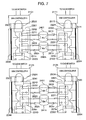
- FIG. 1 is a conceptive diagram showing an example of the construction of a magnetic disk subsystem according to an embodiment of the invention
- FIG. 2 is a diagram showing an example of the construction subordinate to disk controllers in the FIG. 1 magnetic disk subsystem according to an embodiment of the invention.
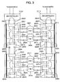
- FIG. 3 is a diagram useful to explain a process of adding a disk controller in the FIG. 2 embodiment of the invention.
- FIG. 4 is a diagram useful to explain the disk controller adding process in the FIG. 2 embodiment of the invention.
- FIG. 5 is a diagram useful in explaining the disk controller adding process in the FIG. 2 embodiment of the invention.
- FIG. 6 is a diagram useful in explaining the disk controller adding process in the FIG. 2 embodiment of the invention.
- FIG. 7 is a diagram useful in explaining the disk controller adding process in the FIG. 2 embodiment of the invention.
- FIG. 8 is a diagram useful in explaining the disk controller adding process in the FIG. 2 embodiment of the invention.
- FIG. 9 is a table showing an example of status type of disk controllers in the FIG. 2 embodiment of the invention.
- FIG. 10 is a table showing an example of status type of disk controllers during the disk controller adding process in the FIG. 2 embodiment of the invention.
- FIG. 11 is a table showing an example of status type of disk controllers during the disk controller adding process in the FIG. 2 embodiment of the invention.
- FIG. 12 is a table showing an example of status type of disk controllers during the disk controller adding process in the FIG. 2 embodiment of the invention.
- FIG. 13 is a table showing an example of status type of disk controllers during the disk controller adding process in the FIG. 2 embodiment of the invention.
- FIG. 14 shows an example of a table of conversion between logical block position and physical block position in the FIG. 2 embodiment of the invention.
- FIG. 15 shows an example of a logical block position-physical block position conversion table during the disk controller adding process in the FIG. 2 embodiment of the invention.
- FIG. 16 shows an example of a logical block position-physical block position conversion table during the disk controller adding process in the FIG. 2 embodiment of the invention.
- FIG. 17 is a flowchart of the disk controller adding process in the FIG. 2 embodiment of the invention.
- FIG. 1 shows the overall construction of a disk subsystem illustrative of an embodiment of the invention.
- a single pair of channel controller A 1101 and channel controller B 1201 are connected to a single host computer 1001 or a plurality of pairs of channel controller A 1101 and channel controller B 1201 are connected to a plurality of host computers 1001 .
- a single pair of disk controller A 1131 and disk controller B 1231 are connected to a single memory device 1301 through a fiber switch A 1141 and a fiber switch B 1241 , respectively, or a plurality of pairs of disk controller A 1131 and disk controller B 1231 are connected to a plurality of memory devices 1301 through the respective fiber switches A 1141 and the respective fiber switches B 1241 .
- the paired disk controller A 1131 and B 1231 are connected further to a single or a plurality of memory devices 1601 through a fiber switch C 1441 and a fiber switch D 1541 , respectively, or through the respective fiber switches C 1441 and the respective fiber switches D 1541 .
- Used as an input/output interface between the disk controller and the memory device is an FC-AL interface.
- Input/output data transmitted/received to/from the host computer 1001 is temporarily stored in cache memories 1111 and 1211 .
- Each of the cache memories 1111 and 1211 uses two planes to assure redundancy.
- the cache memories 1111 and 1211 are connected to the channel controller A 1101 through cache switches A 1121 and 1122 .
- the cache memories 1111 and 1211 are also connected to the channel controller B 1201 through cache switches B 1221 and 1222 .
- the cache memories 1111 and 1211 are connected to the disk controller A 1131 through the cache switches A 1121 and 1122 and are connected to the disk controller B 1231 through the cache switches B 1221 and 1222 .
- Communication between the channel controller A 1101 and the disk controller A 1131 and that between the channel controller B 1201 and the disk controller B 1231 are carried out through common memories (shared memories) 1112 and 1212 .
- the common memories 1112 and 1212 are connected to the channel controller A 1101 through the cache switches A 1121 and 1122 and are connected to the channel controller B 1201 through the cache switches 1221 and 1222 .
- the common memories 1112 and 1212 are also connected to the disk controller A 1131 through the cache switches 1121 and 1122 and are connected to the disk controller B 1231 through the cache switches B 1221 and 1222 .
- the channel controller A 1101 When the channel controller A 1101 receives a data read request from the host computer 1001 , it writes a command “read data from a block position (hereinafter referred to as a logical block) requested by the host computer and write the data in a cache” into the common memory 1112 or 1212 through the cache switch A 1121 or 1122 .
- the disk controller A 1131 or disk controller B 1231 After the disk controller A 1131 or disk controller B 1231 has practiced conversion between logical block and physical block, it recursively monitors the common memories 1112 and 1212 to check if there is a command to input/output data to/from a memory device block position (hereinafter referred to as a physical block) connected to its own.
- the disk controller A 1131 or disk controller B 1231 carries out the logical-physical block conversion and confirms if an FC-AL interface connected to the memory device 1301 or 1601 described in the command is not registered as a blocked port in the common memory 1112 or 1212 .
- the disk controller A 1131 reads data from the memory device 1301 or 1601 through the fiber switch A 1141 or fiber switch C 1441 or the disk controller B 1231 reads data from the memory device 1301 or 1601 through the fiber switch B 1241 or fiber switch D 1541 .
- the disk controller A 1131 writes the data into the cache memory 1111 or 1211 through the cache switch A 1121 or 1122 or the disk controller B 1231 writes the data into the cache memory 1111 or 1211 through cache switch B 1221 or 1222 . Then, the disk controller A 1131 or disk controller B 1231 writes a “read end” report in the common memory 1112 or 1122 through the cache switch A 1121 or 1122 or the cache switch B 1221 or 1222 .
- the channel controller A 1101 recursively monitors the common memories 1112 and 1212 through the cache switches A 1121 and 1122 to check if read operation ends. When recognizing that a “read end” report is described in the common memory 1112 or 1212 , the channel controller A 1101 transfers the requested data stored in the cache memory 1111 or 1211 to the host computer 1001 through the cache switch A 1121 or 1122 .
- the channel controller B 1201 When the channel controller B 1201 receives a data write request from the host computer 1001 , it writes data of the host computer 1001 into the cache memories 1111 and 1211 through the cache switches B 1221 and 1222 . Thereafter, the channel controller B 1201 writes a command “data write” into the common memory 1112 or 1212 through the cache switch B 1221 or 1222 .
- disk controller A 1131 or disk controller B 1231 which practices the logical-physical block conversion and thereafter recursively monitors the common memories to check if there is an input/output command to/from a physical block of a memory device connected to its own, recognizes that the “data write” command is written in the common memory 1112 or 1212 , it reads data from the cache memory 1111 or 1211 through the cache switch A 1121 or 1122 or the cache switch B 1221 or 1222 and following the logical-physical conversion, confirms if an FC-AL interface connected to the memory device including the physical block is not registered as a blocked port.
- the disk controller A 1131 or disk controller B 1231 writes the data into the memory device 1301 or 1601 through the fiber switch A 1141 or C 1441 or through the fiber switch B 1241 or D 1541 .
- a disk controller A 2101 is connected to an FC-AL interface connector 2202 of fiber switch 2201 through an FC-AL interface 2502 for performing paired one-way transmission.
- the fiber switch 2201 includes a single or a plurality of bypass switches 2211 to 221 n which are connected to magnetic disks Al 2401 to An 240 n , respectively, through FC-AL interfaces 2601 to 260 n , respectively.
- the individual bypass switches 2211 to 221 n are connected to a switching bus 2204 .
- the disk controller A 2101 is connected to the switching bus 2204 through a switching bus interface 2501 .
- the disk controller A 2101 controls the switching bus 2204 to change the bypass status of the bypass switches 2211 to 221 n , thus making it possible to interrupt a signal flow to the FC-AL interfaces 2601 to 260 n connected to the magnetic disks Al 2401 to An 240 n .
- the fiber switch 2201 also includes a bypass switch 2203 . With the bypass switch 2203 closed outward, the fiber switch 2201 can be connected to another fiber switch 2241 through an FC-Al interface 2504 and a switching bus interface 2503 .
- the fiber switch 2241 includes a single or a plurality of bypass switches 2251 to 225 n which are connected to magnetic disks B 1 2411 to Bn 241 n , respectively, through FC-AL interfaces 2621 to 262 n .
- the individual bypass switches 2251 to 225 n are connected to a switching bus 2244 .
- the disk controller A 2101 is connected to the switching bus 2244 through the switching bus interface 2501 , switching bus 2204 and switching bus interface 2503 .
- the disk controller A 2101 controls the switching bus 2244 to change the bypass status of the bypass switches 2251 to 225 n , thus making it possible to interrupt a signal flow to the FC-AL interfaces 2621 to 262 n connected to the magnetic disks B 1 2411 to Bn 241 n .
- a disk controller B 2111 is connected to an FC-AL interface connector 2222 of fiber switch 2221 through an FC-AL interface 2512 for paired one-way transmission.
- the fiber switch 2221 includes a single or a plurality of bypass switches 2231 to 223 n which are connected to the magnetic disks Al 2401 to An 240 n , respectively, through FC-AL interfaces 2611 to 261 n , respectively.
- the individual bypass switches 2231 to 223 n are connected to a switching bus 2224 .
- the disk controller B 2111 is connected to the switching bus 2224 through a switching bus interface 2511 .
- the disk controller B 2111 changes the bypass status of the bypass switches 2231 go 223 n , thus making it possible to interrupt a signal flow to the FC-AL interfaces 2611 to 261 n connected to the magnetic disks Al 2401 to An 240 n .
- the fiber switch 2221 also includes a bypass switch 2223 and with this bypass switch closed outward, the fiber switch 2221 can be connected to another fiber switch 2261 through an FC-AL interface 2514 and a switching bypass interface 2262 .
- the fiber switch 2261 includes a single or a plurality of bypass switches 2271 to 227 n which are connected to the magnetic disks B 1 2411 to Bn 241 n , respectively, through FC-AL interfaces 2631 to 263 n , respectively.
- the individual bypass switches 2271 to 227 n are connected to a switching bus 2264 .
- the disk controller B 2111 is connected to the switching bus 2264 through the switching bus interface 2511 , switching bus 2224 and switching bus interface 2513 and it changes the bypass status of the bypass switches 2271 to 227 n so as to make it possible to interrupt a signal flow to the FCAL interfaces 2631 to 263 n connected to the magnetic disks B 1 2411 to Bn 241 n.
- control information indicative of status information for each disk controller includes mounting information as to whether the disk controller is mounted and status indicative of the operating status and is stored in the common memories 1112 and 1212 shown in FIG. 1.
- the disk controller A is mounted to exhibit normal status
- the disk controller B is also mounted to exhibit normal status
- a disk controller A′ is not mounted to exhibit blocked status
- a disk controller B′ is not mounted to exhibit blocked status.
- FIG. 14 there is illustrated an example of a table for conversion between logical block position and physical block position in the construction status of FIG. 2.
- the present table is stored in the common memories 1112 and 1212 shown in FIG. 1.
- step 5001 the status of disk controller A 2101 stored in the common memories 1112 and 1212 is changed to “mounted-blocked” as shown in FIG. 10 to prevent the disk controller A 2101 side from receiving an I/O request.
- step 5002 the bypass switches 2211 to 221 n and 2251 to 225 n are opened as shown in FIG. 3 to interrupt signals from the drive A 1 2401 to drive An 240 n and from the drive B 1 2411 to drive Bn 241 n and the fiber switch 2203 is closed inward to interrupt signals between the fiber switch 2241 and the fiber switch 2201 .
- the switching bus interface 2503 and FC-AL interface 2504 are removed in the step 5002 , and a disk controller A′ 2121 shown in FIG. 4 is added and connected to the fiber switch 2241 by using a switching bus interface 2523 and an FC-AL interface 2524 (step 5003 ).
- the fiber switch 2241 has the function to connect two systems of disk controller or fiber switch, only a disk controller of one system may be connected and in this construction, input/output of data transfer to/from the plurality of memory devices A and the plurality of memory devices B may be interrupted by means of a switch circuit and thereafter, a controller of the other system may be connected, thereby completing addition of the disk controllers.
- step 5004 the logical block position-physical block position conversion table stored in the common memories 1112 and 1212 is updated as shown in FIG. 15 in order that the controller type corresponding to logical block positions 10000000 to 1000000m and 100n0000 to 100n000m can be changed from A to A′.
- step 5005 the fiber switches 2211 to 221 n and fiber switches 2251 to 225 n are closed as shown in FIG. 5 to release the bypasses associated with the drive A 1 2401 to An 240 n and the B 1 2411 to Bn 141 n .
- step 5006 the attribute of the controller A 2101 stored in the common memories 1112 and 1212 of FIG. 1 is changed to “mounted-normal” as shown in FIG. 11 and the status of the controller A′ 2121 is changed to “mounted-normal”, thereby placing the controller A and controller A′ in usable condition.
- step 5011 the status of disk controller B 2111 stored in the common memories 1112 and 1212 is changed to “mounted-blocked” as shown in FIG. 12.
- step 5012 the bypass switches 2231 to 223 n and 2271 to 227 n are opened as shown in FIG. 6 to interrupt signals to/from the drives A 1 2401 to An 240 n and B 1 2411 to Bn 241 n and the fiber switch 2223 is closed inward to interrupt signals between the fiber switch 2221 and the fiber switch 2261 .
- the switching bus interface 2513 and FC-AL interface 2514 are removed in FIG. 6, and a disk controller B′ 2131 shown in FIG.
- step 5013 if the fiber switch 2261 has the function to connect two systems of disk controller or fiber switch, only a controller of one system may be connected and in this construction, input/output of data transfer to/from the plurality of memory devices A and the plurality of memory devices B may be interrupted by means of a switch circuit and thereafter, a controller of the other system may be connected, thus completing the addition of the disk controllers.
- step 5014 the logical block position-physical block position conversion table stored in the common memories 1112 and 1212 shown in FIG. 1 is updated as shown in FIG.
- step 5015 the fiber switches 2231 to 223 n and fiber switches 2271 to 227 n are closed as shown in FIG. 8 to release the bypasses for the drive A 1 2401 to An 240 n and B 1 2411 to Bn 241 n .
- step 5016 the status of controller B 2111 stored in the common memories of FIG. 1 is changed to “mounted-normal” and the status of controller B′ 2131 is changed to “mounted-normal”, thus placing the controller B and controller B′ in usable condition.
Landscapes
- Engineering & Computer Science (AREA)
- Theoretical Computer Science (AREA)
- Human Computer Interaction (AREA)
- Physics & Mathematics (AREA)
- General Engineering & Computer Science (AREA)
- General Physics & Mathematics (AREA)
- Computer Networks & Wireless Communication (AREA)
- Signal Processing For Digital Recording And Reproducing (AREA)
- Memory System Of A Hierarchy Structure (AREA)
Applications Claiming Priority (2)
| Application Number | Priority Date | Filing Date | Title |
|---|---|---|---|
| JP2002104647A JP2003296034A (ja) | 2002-04-08 | 2002-04-08 | ディスクサブシステムとその制御方法 |
| JP2002-104647 | 2002-04-08 |
Publications (1)
| Publication Number | Publication Date |
|---|---|
| US20030191890A1 true US20030191890A1 (en) | 2003-10-09 |
Family
ID=28672332
Family Applications (1)
| Application Number | Title | Priority Date | Filing Date |
|---|---|---|---|
| US10/223,828 Abandoned US20030191890A1 (en) | 2002-04-08 | 2002-08-19 | Disk subsystem and a method for controlling the disk subsystem |
Country Status (2)
| Country | Link |
|---|---|
| US (1) | US20030191890A1 (enExample) |
| JP (1) | JP2003296034A (enExample) |
Cited By (12)
| Publication number | Priority date | Publication date | Assignee | Title |
|---|---|---|---|---|
| US20040078517A1 (en) * | 2002-10-17 | 2004-04-22 | Hitachi, Ltd. | Disk array device, method for controlling the disk array device and storage system |
| US20050033912A1 (en) * | 2003-08-05 | 2005-02-10 | Hitachi, Ltd. | Data managing method, disk storage unit, and disk storage system |
| US20050204096A1 (en) * | 2004-03-12 | 2005-09-15 | Kentaro Shimada | Storage systems and methods of controlling cache memory of storage systems |
| US20050278581A1 (en) * | 2004-05-27 | 2005-12-15 | Xiaoming Jiang | Storage control system and operating method for storage control system |
| US7035973B2 (en) | 2003-04-08 | 2006-04-25 | Hitachi, Ltd. | Storage control apparatus and method for controlling logical volumes by referring to mounting information indicating mounting states of the logical volumes |
| US20060277445A1 (en) * | 2005-06-06 | 2006-12-07 | Azuma Kano | Disk array apparatus and method for controlling the same |
| US20160071608A1 (en) * | 2006-11-29 | 2016-03-10 | Rambus Inc. | Dynamic memory rank configuration |
| US10372364B2 (en) * | 2016-04-18 | 2019-08-06 | Super Micro Computer, Inc. | Storage enclosure with daisy-chained sideband signal routing and distributed logic devices |
| US20220357867A1 (en) * | 2021-05-06 | 2022-11-10 | EMC IP Holding Company LLC | Method for adding disks in a raid system having a protection pool of storage units |
| US11640343B2 (en) | 2021-05-06 | 2023-05-02 | EMC IP Holding Company LLC | Method for migrating data in a raid system having a protection pool of storage units |
| US11733922B2 (en) | 2021-05-06 | 2023-08-22 | EMC IP Holding Company LLC | Method for data reconstruction in a RAID system having a protection pool of storage units |
| US11989449B2 (en) | 2021-05-06 | 2024-05-21 | EMC IP Holding Company LLC | Method for full data reconstruction in a raid system having a protection pool of storage units |
Citations (2)
| Publication number | Priority date | Publication date | Assignee | Title |
|---|---|---|---|---|
| US20020019897A1 (en) * | 1997-11-14 | 2002-02-14 | Sun Microsystems, Inc. | Partitioning of storage channels using programmable switches |
| US6567890B1 (en) * | 1999-06-30 | 2003-05-20 | Emc Corporation | Fibre channel port by-pass selector section for dual ported disk drives |
-
2002
- 2002-04-08 JP JP2002104647A patent/JP2003296034A/ja active Pending
- 2002-08-19 US US10/223,828 patent/US20030191890A1/en not_active Abandoned
Patent Citations (2)
| Publication number | Priority date | Publication date | Assignee | Title |
|---|---|---|---|---|
| US20020019897A1 (en) * | 1997-11-14 | 2002-02-14 | Sun Microsystems, Inc. | Partitioning of storage channels using programmable switches |
| US6567890B1 (en) * | 1999-06-30 | 2003-05-20 | Emc Corporation | Fibre channel port by-pass selector section for dual ported disk drives |
Cited By (32)
| Publication number | Priority date | Publication date | Assignee | Title |
|---|---|---|---|---|
| US7139880B2 (en) | 2002-10-17 | 2006-11-21 | Hitachi, Ltd. | Disk array device, method for controlling the disk array device and storage system |
| US7487298B2 (en) | 2002-10-17 | 2009-02-03 | Hitachi, Ltd. | Disk array device, method for controlling the disk array device and storage system |
| US20080016285A1 (en) * | 2002-10-17 | 2008-01-17 | Seiji Kaneko | Disk array device, method for controlling the disk array device and storage system |
| US7287125B2 (en) | 2002-10-17 | 2007-10-23 | Hitachi, Ltd. | Disk array device, method for controlling the disk array device and storage system |
| US20070033342A1 (en) * | 2002-10-17 | 2007-02-08 | Seiji Kaneko | Disk array device, method for controlling the disk array device and storage system |
| US20040078517A1 (en) * | 2002-10-17 | 2004-04-22 | Hitachi, Ltd. | Disk array device, method for controlling the disk array device and storage system |
| US7133976B2 (en) | 2002-10-17 | 2006-11-07 | Hitachi, Ltd. | Disk array device, method for controlling the disk array device and storage system |
| US7035973B2 (en) | 2003-04-08 | 2006-04-25 | Hitachi, Ltd. | Storage control apparatus and method for controlling logical volumes by referring to mounting information indicating mounting states of the logical volumes |
| US7418549B2 (en) | 2003-08-05 | 2008-08-26 | Hitachi, Ltd. | Storage system with disk array controllers that independently manage data transfer |
| US20050033912A1 (en) * | 2003-08-05 | 2005-02-10 | Hitachi, Ltd. | Data managing method, disk storage unit, and disk storage system |
| US7814270B2 (en) | 2004-03-12 | 2010-10-12 | Hitachi, Ltd. | Storage systems and methods of controlling cache memory of storage systems |
| US7249221B2 (en) * | 2004-03-12 | 2007-07-24 | Hitachi, Ltd. | Storage system having network channels connecting shared cache memories to disk drives |
| US20070245091A1 (en) * | 2004-03-12 | 2007-10-18 | Kentaro Shimada | Storage systems and methods of controlling cache memory of storage systems |
| US20070245089A1 (en) * | 2004-03-12 | 2007-10-18 | Kentaro Shimada | Storage systems and methods of controlling cache memory of storage systems |
| US20070250665A1 (en) * | 2004-03-12 | 2007-10-25 | Kentaro Shimada | Storage systems and methods of controlling cache memory of storage systems |
| US20050204096A1 (en) * | 2004-03-12 | 2005-09-15 | Kentaro Shimada | Storage systems and methods of controlling cache memory of storage systems |
| US7111087B2 (en) * | 2004-05-27 | 2006-09-19 | Hitachi, Ltd. | Storage control system and operating method for storage control system |
| US20050278581A1 (en) * | 2004-05-27 | 2005-12-15 | Xiaoming Jiang | Storage control system and operating method for storage control system |
| US20060277445A1 (en) * | 2005-06-06 | 2006-12-07 | Azuma Kano | Disk array apparatus and method for controlling the same |
| US20090292945A1 (en) * | 2005-06-06 | 2009-11-26 | Azuma Kano | Disk array apparatus and method for controlling the same |
| US7607035B2 (en) * | 2005-06-06 | 2009-10-20 | Hitachi, Ltd. | Disk array apparatus and method for controlling the same |
| US7941693B2 (en) | 2005-06-06 | 2011-05-10 | Hitachi, Ltd. | Disk array apparatus and method for controlling the same |
| US8423818B2 (en) | 2005-06-06 | 2013-04-16 | Hitachi, Ltd. | Disk array apparatus and method for controlling the same |
| US11244727B2 (en) * | 2006-11-29 | 2022-02-08 | Rambus Inc. | Dynamic memory rank configuration |
| US20160071608A1 (en) * | 2006-11-29 | 2016-03-10 | Rambus Inc. | Dynamic memory rank configuration |
| US12002513B2 (en) | 2006-11-29 | 2024-06-04 | Rambus Inc. | Self-annealing data storage system |
| US10372364B2 (en) * | 2016-04-18 | 2019-08-06 | Super Micro Computer, Inc. | Storage enclosure with daisy-chained sideband signal routing and distributed logic devices |
| US20220357867A1 (en) * | 2021-05-06 | 2022-11-10 | EMC IP Holding Company LLC | Method for adding disks in a raid system having a protection pool of storage units |
| US11640343B2 (en) | 2021-05-06 | 2023-05-02 | EMC IP Holding Company LLC | Method for migrating data in a raid system having a protection pool of storage units |
| US11733922B2 (en) | 2021-05-06 | 2023-08-22 | EMC IP Holding Company LLC | Method for data reconstruction in a RAID system having a protection pool of storage units |
| US11748016B2 (en) * | 2021-05-06 | 2023-09-05 | EMC IP Holding Company LLC | Method for adding disks in a raid system having a protection pool of storage units |
| US11989449B2 (en) | 2021-05-06 | 2024-05-21 | EMC IP Holding Company LLC | Method for full data reconstruction in a raid system having a protection pool of storage units |
Also Published As
| Publication number | Publication date |
|---|---|
| JP2003296034A (ja) | 2003-10-17 |
Similar Documents
| Publication | Publication Date | Title |
|---|---|---|
| JP4294142B2 (ja) | ディスクサブシステム | |
| JP4477906B2 (ja) | ストレージシステム | |
| US6425049B1 (en) | Disk array system and method of changing the configuration of the disk array system | |
| US7213141B2 (en) | Storage subsystem and storage controller | |
| US8086775B2 (en) | Storage system effectively using free ports | |
| KR101506368B1 (ko) | 직접-연결 저장 시스템을 위한 능동-능동 장애 극복 | |
| EP1837750A2 (en) | Computer system for controlling allocation of physical links and method thereof | |
| JP4009470B2 (ja) | 冗長データ格納システム | |
| US20060203857A1 (en) | System and method for data multiplexing | |
| US7143306B2 (en) | Data storage system | |
| US8402195B2 (en) | Storage system mounted with plurality of processors | |
| JP2003296034A (ja) | ディスクサブシステムとその制御方法 | |
| JPH11249814A (ja) | スイッチ機構およびこれを有するディスクアレイ装置およびコンピュータシステム | |
| JP2003296034A5 (enExample) | ||
| US7472210B2 (en) | Multiplexing and bypass circuit for interfacing either single or dual ported drives to multiple storage processors | |
| EP0729098B1 (en) | Information storage controller | |
| JP2000347812A (ja) | 情報処理装置およびディスクアレイ装置 | |
| TW200521965A (en) | RAID system with fail over and load balance | |
| JP4025032B2 (ja) | ディスク制御装置、および、そのデータアクセス方法 | |
| JP4444636B2 (ja) | ディスクサブシステム | |
| JP4892275B2 (ja) | ストレージシステム及びその構成変更方法 | |
| JP2001022526A (ja) | 外部記憶装置およびその動作方法 | |
| KR100347527B1 (ko) | 단일 광채널 중재루프를 이용한 래이드 시스템의 구조 | |
| US7120161B1 (en) | Network adapter and method of using same | |
| JPH03268153A (ja) | 入出力制御装置 |
Legal Events
| Date | Code | Title | Description |
|---|---|---|---|
| AS | Assignment |
Owner name: HITACHI, LTD., JAPAN Free format text: ASSIGNMENT OF ASSIGNORS INTEREST;ASSIGNORS:OKAMOTO, TAKEKI;SATOH, TAKAO;REEL/FRAME:013217/0753 Effective date: 20020702 |
|
| STCB | Information on status: application discontinuation |
Free format text: ABANDONED -- FAILURE TO RESPOND TO AN OFFICE ACTION |