US20020155944A1 - Ceramic polycrystal and method of manufacturing the same - Google Patents
Ceramic polycrystal and method of manufacturing the same Download PDFInfo
- Publication number
- US20020155944A1 US20020155944A1 US10/099,450 US9945002A US2002155944A1 US 20020155944 A1 US20020155944 A1 US 20020155944A1 US 9945002 A US9945002 A US 9945002A US 2002155944 A1 US2002155944 A1 US 2002155944A1
- Authority
- US
- United States
- Prior art keywords
- ceramic
- polycrystal
- less
- ceramic polycrystal
- compact
- Prior art date
- Legal status (The legal status is an assumption and is not a legal conclusion. Google has not performed a legal analysis and makes no representation as to the accuracy of the status listed.)
- Abandoned
Links
Images


Classifications
-
- C—CHEMISTRY; METALLURGY
- C04—CEMENTS; CONCRETE; ARTIFICIAL STONE; CERAMICS; REFRACTORIES
- C04B—LIME, MAGNESIA; SLAG; CEMENTS; COMPOSITIONS THEREOF, e.g. MORTARS, CONCRETE OR LIKE BUILDING MATERIALS; ARTIFICIAL STONE; CERAMICS; REFRACTORIES; TREATMENT OF NATURAL STONE
- C04B35/00—Shaped ceramic products characterised by their composition; Ceramics compositions; Processing powders of inorganic compounds preparatory to the manufacturing of ceramic products
- C04B35/01—Shaped ceramic products characterised by their composition; Ceramics compositions; Processing powders of inorganic compounds preparatory to the manufacturing of ceramic products based on oxide ceramics
- C04B35/10—Shaped ceramic products characterised by their composition; Ceramics compositions; Processing powders of inorganic compounds preparatory to the manufacturing of ceramic products based on oxide ceramics based on aluminium oxide
- C04B35/111—Fine ceramics
- C04B35/115—Translucent or transparent products
-
- C—CHEMISTRY; METALLURGY
- C04—CEMENTS; CONCRETE; ARTIFICIAL STONE; CERAMICS; REFRACTORIES
- C04B—LIME, MAGNESIA; SLAG; CEMENTS; COMPOSITIONS THEREOF, e.g. MORTARS, CONCRETE OR LIKE BUILDING MATERIALS; ARTIFICIAL STONE; CERAMICS; REFRACTORIES; TREATMENT OF NATURAL STONE
- C04B35/00—Shaped ceramic products characterised by their composition; Ceramics compositions; Processing powders of inorganic compounds preparatory to the manufacturing of ceramic products
- C04B35/622—Forming processes; Processing powders of inorganic compounds preparatory to the manufacturing of ceramic products
- C04B35/626—Preparing or treating the powders individually or as batches ; preparing or treating macroscopic reinforcing agents for ceramic products, e.g. fibres; mechanical aspects section B
- C04B35/63—Preparing or treating the powders individually or as batches ; preparing or treating macroscopic reinforcing agents for ceramic products, e.g. fibres; mechanical aspects section B using additives specially adapted for forming the products, e.g.. binder binders
- C04B35/632—Organic additives
Definitions
- the present invention relates to a ceramic polycrystal to be used as a constitutive part of an arc tube of a high-pressure discharge lamp such as a metal halide lamp and also relates to a method of manufacturing such a ceramic polycrystal.
- One of ceramic polycrystals known in the art has been prepared by sintering alumina polycrystal as shown in FIG. 1.
- the crystalline direction of such an alumina polycrystal 1 is irregular, so that the linear transmittance of light through the alumina polycrystal 1 can be lowered.
- the alumina polycrystal 1 is a doubly refracting transmission, the amount of light 3 vertically generated from one side of the alumina polycrystal is decreased with respect to the amount of light 2 vertically incident on the opposite side of the alumina polycrystal. Consequently, it is difficult for the alumina polycrystal 1 to obtain a linear transmittance of not less than 8% which is desired for an arc tube.
- the ceramic polycrystalline sintered bodies comprised of cubic-system materials such as YAG and Y 2 O 3 have disadvantages.
- a ceramic polycrystal having a comparatively high linear transmittance of not less than 8% in addition to have a heat resistance enough to be used in an arc tube.
- It is another object of the present invention is to provide a method for manufacturing of such a novel ceramic polycrystal.
- a ceramic polycrystalline comprises crystals, where each crystalline particle has a crystalline structure selected from triclinic, monoclinic, rhombic, tetragonal, trigonal, and hexagonal system with an average grain size in the range of 5 ⁇ m to 50 ⁇ m and a linear transmittance of 8% or more.
- the ceramic polycrystal of the present invention has a crystalline structure of a triclinic, monoclinic, rhombic, tetragonal, trigonal, or hexagonal system.
- the ceramic polycrystal has a crystalline structure except a cubic system. Consequently, there is no fear to occur any cracks under temperature variations from 1200° C. to a room temperature (about 27° C.), whereas such cracks occur in the conventional ceramic polycrystals having cubic crystalline system.
- the influence of double refraction becomes remarkable if the average grain size is less than 5 ⁇ m. In this case, there is a fear of decreasing the linear transmittance of the ceramic polycrystalline. In the average grain size is greater than 50 ⁇ m, on the other hand, the strength of the ceramic polycrystal becomes low. According to the first aspect of the present invention, therefore, crystals that made up the ceramic polycrystal of the present invention have an average grain size of 5 to 50 ⁇ m, so that it can be prevented from the decrease in linear transmittance and the decrease in strength. In this case, preferably, a grain orientation rate in the ceramic polycrystal may be not less than 20%.
- the ceramic polycrystal has an appropriate crystalline structure (e.g., a most stable crystalline structure) depending on its kind.
- a most stable crystalline structure e.g., a most stable crystalline structure
- the ceramic polycrystal is made of alumina, it generally becomes most stable when the crystalline structure is of a hexagonal system.
- linear transmittance means that the ratio between the amount of light incident to the predetermined side of the ceramic polycrystal and the amount of light generated from the opposite side of the ceramic polycrystal in the same direction as that of the incident light. Thus, the amount of output light in the direction different from the incident light is not considered in the calculation of linear transmittance.
- total optical transmittance means that the ratio between the amount of light incident to the predetermined side of the ceramic polycrystal and the amount of light generated from the opposite side of the ceramic polycrystal in all directions.
- grain orientation rate means the ratio of the cross-sectional area of oriented crystalline particles to the cross-sectional area of the whole crystalline particles.
- a method for manufacturing a ceramic polycrystal comprising the steps of: preparing a ceramic compact with aligning not less than 20% of plate-like crystalline particles in a flowing direction of slurry or greenware, calcining the ceramic compact to provide a calcined compact, and obtaining a sintered compact.
- the present invention allows the ceramic polycrystal having a thermal stability sufficient to be used in an arc tube and also having a comparatively higher linear transmittance of not less than 8%.
- the alignment of not less than 20% of plate-like crystalline particles in a flow direction of slurry or greenware may be attained using the means of slip casting, gel casting, or extrusion molding or casting.
- FIG. 1 is a cross sectional schematic diagram for illustrating a conventional ceramic polycrystal
- FIG. 2 is a cross sectional schematic diagram for illustrating a ceramic polycrystal in accordance of the present invention.
- FIG. 3 is a flowchart for illustrating the steps in the method for manufacturing a ceramic polycrystal in accordance with the present invention.
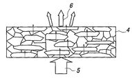
- FIG. 2 is a cross sectional schematic diagram for illustrating a ceramic polycrystal as one of preferred embodiments of the present invention.
- a ceramic polycrystal 4 has a crystalline structure of triclinic, monoclinic, rhombic, tetragonal, trigonal, or hexagonal system.
- An average grain size of crystalline particles in the ceramic polycrystal 4 is in the range of 5 ⁇ m to 50 ⁇ m.
- the linear transmission of the ceramic polycrystal 4 i.e., the ratio of the amount of output light 6 vertically generated from one side of the ceramic polycrystal 4 to the amount of light 5 vertically incident on the opposite side of the ceramic polycrystal 4
- the grain orientation rate of the ceramic polycrystal 4 may be not less than 20%.
- the ceramic polycrystal 4 comprises crystalline particles having a crystalline structure selected from the group of triclinic, monoclinic, rhombic, tetragonal, trigonal, and hexagonal systems.
- the ceramic polycrystal is comprised of crystalline particles with a crystalline structure except a cubic system. Therefore, there is no fear to occur any cracks under temperature variations from 1200° C. to a room temperature (about 27° C.).
- crystalline particles that made up the ceramic polycrystal of the present invention have an average grain size of 5 to 50 ⁇ m, so that it can be prevented from the decrease in linear transmittance which will be caused by the growth of crystal. Consequently, the ceramic polycrystal 4 has an excellent thermal stability enough to be used in an arc tube and also has a comparatively higher linear transmittance of not less than 8%.
- FIG. 3 is a flowchart for illustrating the steps in the method for manufacturing a ceramic polycrystal in accordance with one of preferred embodiments of the present invention.
- the ceramic polycrystal is an Al 2 O 3 —MgO-based alumina polycrystal.
- an ⁇ -alumina powdery material comprising plate-like crystalline particles with an average grain size of 0.5 ⁇ m is mixed with a predetermined amount of water so as to obtain a mixture having 250 ppm of MgO powders with an average grain size of 0.1 ⁇ m and 50% of powder-slurry concentration. Then, a dispersant such as polycarboxylate ammonium is added in the mixture, followed by crushing with a pot mill for 20 hours.
- the mixture was subjected to a casting using a plaster mold to shape it into a compact in which not less than 20% of plate-like crystalline particles are aligned in a flow direction of slurry or greenware.
- the resulting compact is calcined at a temperature of 850° C. under atmospheric conditions.
- the resulting calcined compact is dipped into a solution of ethylenediaminetetraacetic acid (EDTA) for chelating, followed by additional calcining at 1200° C. under atmospheric conditions.
- EDTA ethylenediaminetetraacetic acid
- the resulting calcined compact is further subjected to sintering at 1850° C. under reduced atmospheric conditions, resulting in a final sintered compact.
- the resulting sintered compact is subjected to the measurement of linear transmittance and the measurement value is 40%.
- the measurement is performed under conditions where a sintered compact of 1 mm in thickness is polished and is then exposed to a linear beam of 3 mm in diameter and 600 nm in wavelength.
- the linear beam passing through the compact is received by a photo receptor of 3 mm in diameter.
- the ratio of the amount of light received by the photo receptor after passing through the sintered compact to the amount of light directly received by the photo receptor is expressed as a percentage.
- the total optical transmittance of the sintered compact obtained as described above is 98% (measurement value).
- the measurement of total optical transmittance is performed by preparing an arc tube using the sintered compact, setting a halogen lamp into the arc tube, and measuring the total amount of light from the halogen lamp using an integrating-sphere photometer.
- the total optical transmittance is the ratio of the amount of light incident to the photometer after passing through the arc tube to the amount of light incident to the photometer without the presence of arc tube, expressed as a percentage.
- the grain orientation rate of the sintered compact obtained as described above i.e., the ratio of the cross-sectional area of the oriented particles to the cross-sectional area of the whole particles
- SEM scanning electron microscope
- the average grain size of the sintered compact is 28 ⁇ m when it is observed by SEM.
- the surface roughness of the sintered compact after polishing the surface thereof is 0.1 ⁇ m when it is measured using a contact-type surface roughness tester which is universally used in the art.
- the ceramic polycrystal of the present invention may be used in another application such as a window material of a semiconductor device in addition to be applied on the arc tube of the high-pressure discharge lamp.
- any one of other alumina polycrystals such as aluminum nitride or other kinds of ceramic polycrystals may be used instead of Al 2 O 3 —MgO alumina polycrystal.
- Greenwave may be used instead of slurry for aligning particles in the predetermined direction.
Landscapes
- Engineering & Computer Science (AREA)
- Chemical & Material Sciences (AREA)
- Ceramic Engineering (AREA)
- Manufacturing & Machinery (AREA)
- Materials Engineering (AREA)
- Structural Engineering (AREA)
- Organic Chemistry (AREA)
- Inorganic Chemistry (AREA)
- Compositions Of Oxide Ceramics (AREA)
- Vessels And Coating Films For Discharge Lamps (AREA)
- Crystals, And After-Treatments Of Crystals (AREA)
- Producing Shaped Articles From Materials (AREA)
Abstract
A ceramic polycrystal and a method of manufacturing such a ceramic polycrystal having thermal stability enough to be used in an arc tube are provided. The ceramic polycrystal has crystalline particles. Each of crystalline particles has a crystalline structure selected from triclinc, monoclinic, rhombi, tetragonal, trigonal, and hexagonal systems, with an average grain size being not less than 5 μm and a linear transmittance being not less than 8%.
Description
- 1. Field of the Invention
- The present invention relates to a ceramic polycrystal to be used as a constitutive part of an arc tube of a high-pressure discharge lamp such as a metal halide lamp and also relates to a method of manufacturing such a ceramic polycrystal.
- 2. Description of the Related Art
- One of ceramic polycrystals known in the art has been prepared by sintering alumina polycrystal as shown in FIG. 1. The crystalline direction of such an alumina polycrystal 1 is irregular, so that the linear transmittance of light through the alumina polycrystal 1 can be lowered. In other words, as the alumina polycrystal 1 is a doubly refracting transmission, the amount of
light 3 vertically generated from one side of the alumina polycrystal is decreased with respect to the amount of light 2 vertically incident on the opposite side of the alumina polycrystal. Consequently, it is difficult for the alumina polycrystal 1 to obtain a linear transmittance of not less than 8% which is desired for an arc tube. - For providing a ceramic polycrystal with a linear transmission of not less than 8%, sintered bodies using cubic-system materials such as YAG and Y 2O3 have been used in the art. In addition, there is a report about the improvement in linear transmittance by minimizing the crystalline grain size of the sintered body of polycrystalline alumina into the order of sub-microns (Morinaga et al., “Effect of Grain Size on Translucency of Polycrystalline Alumina”, Journal of the Mining and Materials Processing Institute of Japan, 471-474, No. 6, vol. 115, 1999).
- However, it is known that the ceramic polycrystalline sintered bodies comprised of cubic-system materials such as YAG and Y 2O3 have disadvantages.
- As one of such disadvantages, cracks occur when the thermal change is occurred form a comparatively high temperature (not less than 1200° C.) to a room temperature (about 27° C.) because of its poor resistance to impact in spite of its high corrosion-resistance. Therefore, polycrystalline sintered bodes made of cubic-system materials are not suitable for arc tubes to be used in lamps that can be heated at temperatures form not less than 1200° C. to a room temperature.
- As another disadvantage, in the case of minimizing the grain size of crystalline particle in the ceramic polycrystalline sintered body into the order of sub-microns, the grain size of crystalline particle increases to the order of microns when the sintered body is heated up to not less than 1200° C., resulting in the decrease in its linear transmittance. For this reason, ceramic polycrystalline sintered bodies with grain sizes of sub-micron orders are also not suitable for lamp arc tubes.
- It is an object of the present invention to provide a ceramic polycrystal having a comparatively high linear transmittance of not less than 8% in addition to have a heat resistance enough to be used in an arc tube.
- According to one aspect of the present invention, there is provided a ceramic polycrystal having a comparatively high linear transmittance of not less than 8% in addition to have a heat resistance enough to be used in an arc tube.
- It is another object of the present invention is to provide a method for manufacturing of such a novel ceramic polycrystal.
- According to one aspect of the present invention, there is provided a ceramic polycrystalline comprises crystals, where each crystalline particle has a crystalline structure selected from triclinic, monoclinic, rhombic, tetragonal, trigonal, and hexagonal system with an average grain size in the range of 5 μm to 50 μm and a linear transmittance of 8% or more.
- With the above-mentioned ceramic polycrystal according to the invention, the ceramic polycrystal of the present invention has a crystalline structure of a triclinic, monoclinic, rhombic, tetragonal, trigonal, or hexagonal system. In other words, the ceramic polycrystal has a crystalline structure except a cubic system. Consequently, there is no fear to occur any cracks under temperature variations from 1200° C. to a room temperature (about 27° C.), whereas such cracks occur in the conventional ceramic polycrystals having cubic crystalline system.
- As explained in the above description of the conventional ceramic polycrystal, the influence of double refraction becomes remarkable if the average grain size is less than 5 μm. In this case, there is a fear of decreasing the linear transmittance of the ceramic polycrystalline. In the average grain size is greater than 50 μm, on the other hand, the strength of the ceramic polycrystal becomes low. According to the first aspect of the present invention, therefore, crystals that made up the ceramic polycrystal of the present invention have an average grain size of 5 to 50 μm, so that it can be prevented from the decrease in linear transmittance and the decrease in strength. In this case, preferably, a grain orientation rate in the ceramic polycrystal may be not less than 20%.
- Here, the ceramic polycrystal has an appropriate crystalline structure (e.g., a most stable crystalline structure) depending on its kind. For example, if the ceramic polycrystal is made of alumina, it generally becomes most stable when the crystalline structure is of a hexagonal system.
- In this specification, the term “linear transmittance” means that the ratio between the amount of light incident to the predetermined side of the ceramic polycrystal and the amount of light generated from the opposite side of the ceramic polycrystal in the same direction as that of the incident light. Thus, the amount of output light in the direction different from the incident light is not considered in the calculation of linear transmittance. On the other hand, the term “total optical transmittance” means that the ratio between the amount of light incident to the predetermined side of the ceramic polycrystal and the amount of light generated from the opposite side of the ceramic polycrystal in all directions. Furthermore, the term “grain orientation rate” means the ratio of the cross-sectional area of oriented crystalline particles to the cross-sectional area of the whole crystalline particles.
- According to another aspect of the present invention, there is provided a method for manufacturing a ceramic polycrystal, comprising the steps of: preparing a ceramic compact with aligning not less than 20% of plate-like crystalline particles in a flowing direction of slurry or greenware, calcining the ceramic compact to provide a calcined compact, and obtaining a sintered compact.
- With the above-mentioned method according to the invention, not less than 20% of plate-like crystalline particles are aligned in a flowing direction of slurry or greenware to obtain a grain orientation rate of not less than 20%. Therefore, the present invention allows the ceramic polycrystal having a thermal stability sufficient to be used in an arc tube and also having a comparatively higher linear transmittance of not less than 8%.
- The alignment of not less than 20% of plate-like crystalline particles in a flow direction of slurry or greenware may be attained using the means of slip casting, gel casting, or extrusion molding or casting.
- Embodiments of the ceramic polycrystal and the method of manufacturing the same according to the present invention will be explained below with reference to the accompanying drawings.
- FIG. 1 is a cross sectional schematic diagram for illustrating a conventional ceramic polycrystal;
- FIG. 2 is a cross sectional schematic diagram for illustrating a ceramic polycrystal in accordance of the present invention; and
- FIG. 3 is a flowchart for illustrating the steps in the method for manufacturing a ceramic polycrystal in accordance with the present invention.
- Hereinafter, we will describe a ceramic polycrystal and a method for manufacturing such a ceramic polycrystal in detail with reference to the attached drawings in accordance with preferred embodiments of the present invention.
- FIG. 2 is a cross sectional schematic diagram for illustrating a ceramic polycrystal as one of preferred embodiments of the present invention. In this embodiment, a ceramic polycrystal 4 has a crystalline structure of triclinic, monoclinic, rhombic, tetragonal, trigonal, or hexagonal system. An average grain size of crystalline particles in the
ceramic polycrystal 4 is in the range of 5 μm to 50 μm. In addition, the linear transmission of the ceramic polycrystal 4 (i.e., the ratio of the amount ofoutput light 6 vertically generated from one side of theceramic polycrystal 4 to the amount oflight 5 vertically incident on the opposite side of the ceramic polycrystal 4) is not less than 8%. Preferably, the grain orientation rate of theceramic polycrystal 4 may be not less than 20%. - According to the present embodiment, as described above, the
ceramic polycrystal 4 comprises crystalline particles having a crystalline structure selected from the group of triclinic, monoclinic, rhombic, tetragonal, trigonal, and hexagonal systems. In other words, the ceramic polycrystal is comprised of crystalline particles with a crystalline structure except a cubic system. Therefore, there is no fear to occur any cracks under temperature variations from 1200° C. to a room temperature (about 27° C.). In addition, crystalline particles that made up the ceramic polycrystal of the present invention have an average grain size of 5 to 50 μm, so that it can be prevented from the decrease in linear transmittance which will be caused by the growth of crystal. Consequently, theceramic polycrystal 4 has an excellent thermal stability enough to be used in an arc tube and also has a comparatively higher linear transmittance of not less than 8%. - FIG. 3 is a flowchart for illustrating the steps in the method for manufacturing a ceramic polycrystal in accordance with one of preferred embodiments of the present invention. In this embodiment, but not limited to, the ceramic polycrystal is an Al 2O3—MgO-based alumina polycrystal.
- First, an α-alumina powdery material comprising plate-like crystalline particles with an average grain size of 0.5 μm is mixed with a predetermined amount of water so as to obtain a mixture having 250 ppm of MgO powders with an average grain size of 0.1 μm and 50% of powder-slurry concentration. Then, a dispersant such as polycarboxylate ammonium is added in the mixture, followed by crushing with a pot mill for 20 hours.
- Subsequently, the mixture was subjected to a casting using a plaster mold to shape it into a compact in which not less than 20% of plate-like crystalline particles are aligned in a flow direction of slurry or greenware. The resulting compact is calcined at a temperature of 850° C. under atmospheric conditions.
- Then, the resulting calcined compact is dipped into a solution of ethylenediaminetetraacetic acid (EDTA) for chelating, followed by additional calcining at 1200° C. under atmospheric conditions. The resulting calcined compact is further subjected to sintering at 1850° C. under reduced atmospheric conditions, resulting in a final sintered compact.
- The resulting sintered compact is subjected to the measurement of linear transmittance and the measurement value is 40%. The measurement is performed under conditions where a sintered compact of 1 mm in thickness is polished and is then exposed to a linear beam of 3 mm in diameter and 600 nm in wavelength. The linear beam passing through the compact is received by a photo receptor of 3 mm in diameter. The ratio of the amount of light received by the photo receptor after passing through the sintered compact to the amount of light directly received by the photo receptor is expressed as a percentage.
- Also, the total optical transmittance of the sintered compact obtained as described above is 98% (measurement value). The measurement of total optical transmittance is performed by preparing an arc tube using the sintered compact, setting a halogen lamp into the arc tube, and measuring the total amount of light from the halogen lamp using an integrating-sphere photometer. In this case, the total optical transmittance is the ratio of the amount of light incident to the photometer after passing through the arc tube to the amount of light incident to the photometer without the presence of arc tube, expressed as a percentage.
- The grain orientation rate of the sintered compact obtained as described above (i.e., the ratio of the cross-sectional area of the oriented particles to the cross-sectional area of the whole particles) is 40% when it is observed using a scanning electron microscope (SEM). In addition, the average grain size of the sintered compact is 28 μm when it is observed by SEM. Furthermore, the surface roughness of the sintered compact after polishing the surface thereof is 0.1 μm when it is measured using a contact-type surface roughness tester which is universally used in the art.
- While the present invention has been described above with reference to certain preferred embodiments, it should be noted that they were present by way of examples only and various changes and/or modifications may be made without departing from the scope of the invention. For example, the ceramic polycrystal of the present invention may be used in another application such as a window material of a semiconductor device in addition to be applied on the arc tube of the high-pressure discharge lamp.
- In the above embodiments, alternatively, any one of other alumina polycrystals such as aluminum nitride or other kinds of ceramic polycrystals may be used instead of Al 2O3—MgO alumina polycrystal.
- Greenwave may be used instead of slurry for aligning particles in the predetermined direction.
- Furthermore, instead of casting, slip casting, extrusion molding, gel casting, or the like may be used.
Claims (4)
1. A ceramic polycrystal comprising crystalline particles, where each of crystalline particles has a crystalline structure selected from triclinc, monoclinic, rhombi, tetragonal, trigonal, and hexagonal systems, with an average grain size being not less than 5 μm and a linear transmittance being not less than 8%.
2. The ceramic polycrystal according to claim 1 , wherein a grain orientation rate is not less than 20%.
3. A method of manufacturing a ceramic polycrystal, comprising the steps of:
preparing a ceramic compact with aligning 20% or more of plate-like crystalline particles in a flowing direction of slurry or greenware;
calcining the ceramic compact to provide a calcined compact;
and obtaining a sintered compact from the ceramic compact.
4. The method according to claim 3 , wherein not less than 20% of plate-like crystalline particles are aligned in a flowing direction of slurry or greenware.
Applications Claiming Priority (2)
| Application Number | Priority Date | Filing Date | Title |
|---|---|---|---|
| JP2001-095,673 | 2001-03-29 | ||
| JP2001095673A JP2002293609A (en) | 2001-03-29 | 2001-03-29 | Ceramic polycrystal body and method of producing the same |
Publications (1)
| Publication Number | Publication Date |
|---|---|
| US20020155944A1 true US20020155944A1 (en) | 2002-10-24 |
Family
ID=18949689
Family Applications (1)
| Application Number | Title | Priority Date | Filing Date |
|---|---|---|---|
| US10/099,450 Abandoned US20020155944A1 (en) | 2001-03-29 | 2002-03-15 | Ceramic polycrystal and method of manufacturing the same |
Country Status (5)
| Country | Link |
|---|---|
| US (1) | US20020155944A1 (en) |
| EP (1) | EP1251112A3 (en) |
| JP (1) | JP2002293609A (en) |
| CN (1) | CN1378990A (en) |
| HU (1) | HUP0201031A2 (en) |
Cited By (10)
| Publication number | Priority date | Publication date | Assignee | Title |
|---|---|---|---|---|
| US20050275142A1 (en) * | 2004-06-10 | 2005-12-15 | Ngk Insulators, Ltd. | Translucent ceramic, a method of producing the same and discharge vessels |
| US20060145625A1 (en) * | 2003-09-22 | 2006-07-06 | Nobuyoshi Takeuchi | Metal halide lamp |
| US20060238880A1 (en) * | 2005-02-08 | 2006-10-26 | Casio Computer Co. , Ltd. | Ceramic hybrid lens and method for manufacturing the same |
| US20110259261A1 (en) * | 2009-01-07 | 2011-10-27 | Ngk Insulators, Ltd. | Reaction vessel for growing single crystal and method for growing single crystal |
| US10221076B2 (en) | 2015-09-30 | 2019-03-05 | Ngk Insulators, Ltd. | Method for producing a plate-like alumina power |
| US10343928B2 (en) | 2014-11-28 | 2019-07-09 | Ngk Insulators, Ltd. | Method for manufacturing plate-like alumina powder and plate-like alumina powder |
| EP3597384A1 (en) * | 2011-02-14 | 2020-01-22 | Inter-University Research Institute Corporation National Institutes of Natural Sciences | Translucent polycrystalline material |
| US10717677B2 (en) | 2015-09-30 | 2020-07-21 | NGK Insultators, Ltd. | Method for producing transparent alumina sintered body |
| US10995934B2 (en) | 2017-01-18 | 2021-05-04 | Ngk Insulators, Ltd. | Optical component including a translucent substrate for adjustable light scattering and lighting device including the same |
| US11105486B2 (en) * | 2018-02-19 | 2021-08-31 | Ngk Insulators, Ltd. | Optic and illumination device |
Families Citing this family (6)
| Publication number | Priority date | Publication date | Assignee | Title |
|---|---|---|---|---|
| CN100398476C (en) * | 2004-10-29 | 2008-07-02 | 株式会社电装 | Production method of polycrystalline ceramic body |
| US20060211568A1 (en) * | 2005-03-16 | 2006-09-21 | Osram Sylvania Inc. | High Total Transmittance Alumina Discharge Vessels Having Submicron Grain Size |
| BRPI0916243B8 (en) * | 2008-08-13 | 2021-06-22 | Ormco Corp | orthodontic brackets |
| EP2371784B1 (en) | 2008-12-25 | 2018-05-16 | Inter-University Research Institute Corporation National Institutes of Natural Sciences | Optical material and production process for the same |
| WO2017057271A1 (en) * | 2015-09-30 | 2017-04-06 | 日本碍子株式会社 | Oriented alumina substrate for epitaxial growth |
| WO2017057272A1 (en) * | 2015-09-30 | 2017-04-06 | 日本碍子株式会社 | Oriented alumina substrate for epitaxial growth |
Family Cites Families (5)
| Publication number | Priority date | Publication date | Assignee | Title |
|---|---|---|---|---|
| EP0667322B1 (en) * | 1993-09-02 | 2001-01-10 | Toto Ltd. | Light-permeable ceramic material and method of manufacturing the same |
| JPH11226923A (en) * | 1998-02-18 | 1999-08-24 | Kagawa Prefecture | Production of light transmitting alumina |
| JP2001048638A (en) * | 1999-08-02 | 2001-02-20 | Agency Of Ind Science & Technol | Production of translucent alumina in slurry casting using gypsum mold |
| JP2001064075A (en) * | 1999-08-30 | 2001-03-13 | Sumitomo Chem Co Ltd | Translucent alumina sintered body and its production |
| JP3401559B2 (en) * | 1999-12-24 | 2003-04-28 | 独立行政法人産業技術総合研究所 | Preparation of Alumina-Glass Composite Porous Body and Method for Producing Translucent Alumina Using Its Porous Mold |
-
2001
- 2001-03-29 JP JP2001095673A patent/JP2002293609A/en not_active Abandoned
-
2002
- 2002-03-15 US US10/099,450 patent/US20020155944A1/en not_active Abandoned
- 2002-03-20 HU HU0201031A patent/HUP0201031A2/en unknown
- 2002-03-27 EP EP02252265A patent/EP1251112A3/en not_active Withdrawn
- 2002-03-29 CN CN02105000.7A patent/CN1378990A/en active Pending
Cited By (14)
| Publication number | Priority date | Publication date | Assignee | Title |
|---|---|---|---|---|
| US20060145625A1 (en) * | 2003-09-22 | 2006-07-06 | Nobuyoshi Takeuchi | Metal halide lamp |
| US20050275142A1 (en) * | 2004-06-10 | 2005-12-15 | Ngk Insulators, Ltd. | Translucent ceramic, a method of producing the same and discharge vessels |
| US20060238880A1 (en) * | 2005-02-08 | 2006-10-26 | Casio Computer Co. , Ltd. | Ceramic hybrid lens and method for manufacturing the same |
| US7471457B2 (en) | 2005-02-08 | 2008-12-30 | Casio Computer Co., Ltd. | Ceramic hybrid lens and method for manufacturing the same |
| US20090072420A1 (en) * | 2005-02-08 | 2009-03-19 | Casio Computer Co., Ltd. | Ceramic hybrid lens and method for manufacturing the same |
| US7790071B2 (en) | 2005-02-08 | 2010-09-07 | Casio Computer Co., Ltd. | Ceramic hybrid lens and method for manufacturing the same |
| US20110259261A1 (en) * | 2009-01-07 | 2011-10-27 | Ngk Insulators, Ltd. | Reaction vessel for growing single crystal and method for growing single crystal |
| EP3597384A1 (en) * | 2011-02-14 | 2020-01-22 | Inter-University Research Institute Corporation National Institutes of Natural Sciences | Translucent polycrystalline material |
| US10343928B2 (en) | 2014-11-28 | 2019-07-09 | Ngk Insulators, Ltd. | Method for manufacturing plate-like alumina powder and plate-like alumina powder |
| US10221076B2 (en) | 2015-09-30 | 2019-03-05 | Ngk Insulators, Ltd. | Method for producing a plate-like alumina power |
| US10717677B2 (en) | 2015-09-30 | 2020-07-21 | NGK Insultators, Ltd. | Method for producing transparent alumina sintered body |
| TWI705951B (en) * | 2015-09-30 | 2020-10-01 | 日商日本碍子股份有限公司 | Method for preparing transparent alumina sintered body |
| US10995934B2 (en) | 2017-01-18 | 2021-05-04 | Ngk Insulators, Ltd. | Optical component including a translucent substrate for adjustable light scattering and lighting device including the same |
| US11105486B2 (en) * | 2018-02-19 | 2021-08-31 | Ngk Insulators, Ltd. | Optic and illumination device |
Also Published As
| Publication number | Publication date |
|---|---|
| CN1378990A (en) | 2002-11-13 |
| JP2002293609A (en) | 2002-10-09 |
| HU0201031D0 (en) | 2002-05-29 |
| HUP0201031A2 (en) | 2002-10-28 |
| EP1251112A2 (en) | 2002-10-23 |
| EP1251112A3 (en) | 2003-10-08 |
Similar Documents
| Publication | Publication Date | Title |
|---|---|---|
| US20020155944A1 (en) | Ceramic polycrystal and method of manufacturing the same | |
| US7247589B2 (en) | Transparent polycrystalline sintered ceramic of cubic crystal structure | |
| Krell et al. | Transparent sintered corundum with high hardness and strength | |
| KR100885199B1 (en) | Translucent rare earth oxide sintered article and method for production thereof | |
| KR100875528B1 (en) | Rare Earth Garnet Sintered Body and Manufacturing Method Thereof | |
| KR102376825B1 (en) | Alumina sintered body and ground substrate for optical element | |
| JP6438588B2 (en) | Translucent rare earth aluminum garnet ceramics | |
| JPS6048466B2 (en) | Manufacturing method of polycrystalline transparent alumina sintered body | |
| JP4723055B2 (en) | Alumina sintered body, manufacturing method thereof, sintered alumina member and arc tube | |
| US20200407280A1 (en) | Rare Earth Oxyfluoride Sintered Body And Method For Producing Same | |
| JP5000934B2 (en) | Translucent rare earth gallium garnet sintered body, manufacturing method thereof and optical device | |
| KR20190031531A (en) | Light wavelength conversion member and light emitting device | |
| JP2939535B2 (en) | Manufacturing method of transparent yttrium oxide sintered body | |
| EP3567016A1 (en) | Method for preparing ceramic molded body for sintering and method for producing ceramic sintered body | |
| JP4251649B2 (en) | Translucent lutetium oxide sintered body and method for producing the same | |
| JPH06227867A (en) | Sintered compact of silicon mitride and its production | |
| JP7135501B2 (en) | Zirconia sintered body and manufacturing method thereof | |
| JP2001158660A (en) | Optically transmitting rare earth-aluminum garnet sintered product and production method therefor | |
| EP3560905B1 (en) | Transparent aln sintered body and production method therefor | |
| JPH05301770A (en) | Polycrystalline transparent ceramic for laser | |
| JPH05294709A (en) | Polycrystalline transparent ceramic for laser | |
| JP2003128465A (en) | Sintered translucent scandium oxide and process for making the same | |
| JPH05301769A (en) | Polycrystalline transparent ceramic for laser | |
| KR20240013752A (en) | Sintered body and its manufacturing method, and orthodontic bracket | |
| JP2671539B2 (en) | Method for producing silicon nitride sintered body |
Legal Events
| Date | Code | Title | Description |
|---|---|---|---|
| AS | Assignment |
Owner name: NGK INSULATORS, LTD., JAPAN Free format text: ASSIGNMENT OF ASSIGNORS INTEREST;ASSIGNORS:KURASHINA, MITSURU;NIIMI, NORIKAZU;YAMAGUCHI, HIROFUMI;REEL/FRAME:013005/0128 Effective date: 20020527 |
|
| STCB | Information on status: application discontinuation |
Free format text: ABANDONED -- FAILURE TO RESPOND TO AN OFFICE ACTION |