US20020100906A1 - Metal coordination compound, luminescence device and display apparatus - Google Patents
Metal coordination compound, luminescence device and display apparatus Download PDFInfo
- Publication number
- US20020100906A1 US20020100906A1 US09/995,609 US99560901A US2002100906A1 US 20020100906 A1 US20020100906 A1 US 20020100906A1 US 99560901 A US99560901 A US 99560901A US 2002100906 A1 US2002100906 A1 US 2002100906A1
- Authority
- US
- United States
- Prior art keywords
- group
- replaced
- luminescence
- carbon atoms
- metal coordination
- Prior art date
- Legal status (The legal status is an assumption and is not a legal conclusion. Google has not performed a legal analysis and makes no representation as to the accuracy of the status listed.)
- Granted
Links
- 229910052751 metal Inorganic materials 0.000 title claims abstract description 60
- 239000002184 metal Substances 0.000 title claims abstract description 60
- 150000001875 compounds Chemical class 0.000 title claims abstract description 54
- 238000004020 luminiscence type Methods 0.000 title claims description 86
- 125000004432 carbon atom Chemical group C* 0.000 claims abstract description 15
- 229910052741 iridium Inorganic materials 0.000 claims abstract description 13
- 125000000217 alkyl group Chemical group 0.000 claims abstract description 12
- 125000004122 cyclic group Chemical group 0.000 claims abstract description 10
- 229910052731 fluorine Inorganic materials 0.000 claims abstract description 10
- 125000001153 fluoro group Chemical group F* 0.000 claims abstract description 10
- 125000004435 hydrogen atom Chemical group [H]* 0.000 claims abstract description 10
- 125000001570 methylene group Chemical group [H]C([H])([*:1])[*:2] 0.000 claims abstract description 10
- 125000001424 substituent group Chemical group 0.000 claims abstract description 9
- 229910052757 nitrogen Inorganic materials 0.000 claims abstract description 6
- 125000005843 halogen group Chemical group 0.000 claims abstract description 5
- 125000000449 nitro group Chemical group [O-][N+](*)=O 0.000 claims abstract description 5
- 125000004433 nitrogen atom Chemical group N* 0.000 claims abstract description 5
- 229910052763 palladium Inorganic materials 0.000 claims abstract description 5
- 125000001997 phenyl group Chemical group [H]C1=C([H])C([H])=C(*)C([H])=C1[H] 0.000 claims abstract description 5
- 229910052697 platinum Inorganic materials 0.000 claims abstract description 5
- 229910052703 rhodium Inorganic materials 0.000 claims abstract description 5
- 125000004665 trialkylsilyl group Chemical group 0.000 claims abstract description 5
- 239000000758 substrate Substances 0.000 claims description 12
- RAXXELZNTBOGNW-UHFFFAOYSA-N imidazole Chemical group C1=CNC=N1 RAXXELZNTBOGNW-UHFFFAOYSA-N 0.000 claims description 9
- JUJWROOIHBZHMG-UHFFFAOYSA-N Pyridine Chemical group C1=CC=NC=C1 JUJWROOIHBZHMG-UHFFFAOYSA-N 0.000 claims description 8
- SMWDFEZZVXVKRB-UHFFFAOYSA-N Quinoline Chemical group N1=CC=CC2=CC=CC=C21 SMWDFEZZVXVKRB-UHFFFAOYSA-N 0.000 claims description 8
- 150000002894 organic compounds Chemical class 0.000 claims description 8
- IOJUPLGTWVMSFF-UHFFFAOYSA-N benzothiazole Chemical group C1=CC=C2SC=NC2=C1 IOJUPLGTWVMSFF-UHFFFAOYSA-N 0.000 claims description 6
- UMJSCPRVCHMLSP-UHFFFAOYSA-N pyridine Natural products COC1=CC=CN=C1 UMJSCPRVCHMLSP-UHFFFAOYSA-N 0.000 claims description 4
- BCMCBBGGLRIHSE-UHFFFAOYSA-N 1,3-benzoxazole Chemical group C1=CC=C2OC=NC2=C1 BCMCBBGGLRIHSE-UHFFFAOYSA-N 0.000 claims description 3
- HYZJCKYKOHLVJF-UHFFFAOYSA-N 1H-benzimidazole Chemical group C1=CC=C2NC=NC2=C1 HYZJCKYKOHLVJF-UHFFFAOYSA-N 0.000 claims description 3
- WTKZEGDFNFYCGP-UHFFFAOYSA-N Pyrazole Chemical group C=1C=NNC=1 WTKZEGDFNFYCGP-UHFFFAOYSA-N 0.000 claims description 3
- 239000011368 organic material Substances 0.000 abstract 1
- 239000010410 layer Substances 0.000 description 52
- 239000000463 material Substances 0.000 description 33
- 238000005401 electroluminescence Methods 0.000 description 28
- BASFCYQUMIYNBI-UHFFFAOYSA-N platinum Substances [Pt] BASFCYQUMIYNBI-UHFFFAOYSA-N 0.000 description 26
- YXFVVABEGXRONW-UHFFFAOYSA-N Toluene Chemical compound CC1=CC=CC=C1 YXFVVABEGXRONW-UHFFFAOYSA-N 0.000 description 21
- 239000012044 organic layer Substances 0.000 description 15
- 0 C.[1*]C1=C([2*])CCC1 Chemical compound C.[1*]C1=C([2*])CCC1 0.000 description 12
- 230000005281 excited state Effects 0.000 description 12
- IJGRMHOSHXDMSA-UHFFFAOYSA-N Atomic nitrogen Chemical compound N#N IJGRMHOSHXDMSA-UHFFFAOYSA-N 0.000 description 11
- KDLHZDBZIXYQEI-UHFFFAOYSA-N palladium Substances [Pd] KDLHZDBZIXYQEI-UHFFFAOYSA-N 0.000 description 11
- XLYOFNOQVPJJNP-UHFFFAOYSA-N water Substances O XLYOFNOQVPJJNP-UHFFFAOYSA-N 0.000 description 11
- 125000000956 methoxy group Chemical group [H]C([H])([H])O* 0.000 description 10
- 230000015572 biosynthetic process Effects 0.000 description 9
- 229910001873 dinitrogen Inorganic materials 0.000 description 9
- 239000000243 solution Substances 0.000 description 9
- 238000006243 chemical reaction Methods 0.000 description 8
- 230000006866 deterioration Effects 0.000 description 8
- 230000005525 hole transport Effects 0.000 description 8
- GKOZUEZYRPOHIO-UHFFFAOYSA-N iridium atom Chemical compound [Ir] GKOZUEZYRPOHIO-UHFFFAOYSA-N 0.000 description 8
- 238000003756 stirring Methods 0.000 description 8
- WYURNTSHIVDZCO-UHFFFAOYSA-N Tetrahydrofuran Chemical compound C1CCOC1 WYURNTSHIVDZCO-UHFFFAOYSA-N 0.000 description 7
- 239000011541 reaction mixture Substances 0.000 description 7
- HEDRZPFGACZZDS-UHFFFAOYSA-N Chloroform Chemical compound ClC(Cl)Cl HEDRZPFGACZZDS-UHFFFAOYSA-N 0.000 description 6
- 125000003438 dodecyl group Chemical group [H]C([H])([H])C([H])([H])C([H])([H])C([H])([H])C([H])([H])C([H])([H])C([H])([H])C([H])([H])C([H])([H])C([H])([H])C([H])([H])C([H])([H])* 0.000 description 6
- 239000003480 eluent Substances 0.000 description 6
- 230000005283 ground state Effects 0.000 description 6
- 125000002572 propoxy group Chemical group [*]OC([H])([H])C(C([H])([H])[H])([H])[H] 0.000 description 6
- 230000007704 transition Effects 0.000 description 6
- UEEXRMUCXBPYOV-UHFFFAOYSA-N iridium;2-phenylpyridine Chemical compound [Ir].C1=CC=CC=C1C1=CC=CC=N1.C1=CC=CC=C1C1=CC=CC=N1.C1=CC=CC=C1C1=CC=CC=N1 UEEXRMUCXBPYOV-UHFFFAOYSA-N 0.000 description 5
- 239000007788 liquid Substances 0.000 description 5
- IBHBKWKFFTZAHE-UHFFFAOYSA-N n-[4-[4-(n-naphthalen-1-ylanilino)phenyl]phenyl]-n-phenylnaphthalen-1-amine Chemical compound C1=CC=CC=C1N(C=1C2=CC=CC=C2C=CC=1)C1=CC=C(C=2C=CC(=CC=2)N(C=2C=CC=CC=2)C=2C3=CC=CC=C3C=CC=2)C=C1 IBHBKWKFFTZAHE-UHFFFAOYSA-N 0.000 description 5
- 238000005424 photoluminescence Methods 0.000 description 5
- 238000010898 silica gel chromatography Methods 0.000 description 5
- 239000002904 solvent Substances 0.000 description 5
- 238000003786 synthesis reaction Methods 0.000 description 5
- 238000012546 transfer Methods 0.000 description 5
- TVIVIEFSHFOWTE-UHFFFAOYSA-K tri(quinolin-8-yloxy)alumane Chemical compound [Al+3].C1=CN=C2C([O-])=CC=CC2=C1.C1=CN=C2C([O-])=CC=CC2=C1.C1=CN=C2C([O-])=CC=CC2=C1 TVIVIEFSHFOWTE-UHFFFAOYSA-K 0.000 description 5
- VFUDMQLBKNMONU-UHFFFAOYSA-N 9-[4-(4-carbazol-9-ylphenyl)phenyl]carbazole Chemical compound C12=CC=CC=C2C2=CC=CC=C2N1C1=CC=C(C=2C=CC(=CC=2)N2C3=CC=CC=C3C3=CC=CC=C32)C=C1 VFUDMQLBKNMONU-UHFFFAOYSA-N 0.000 description 4
- CSCPPACGZOOCGX-UHFFFAOYSA-N Acetone Chemical compound CC(C)=O CSCPPACGZOOCGX-UHFFFAOYSA-N 0.000 description 4
- RTZKZFJDLAIYFH-UHFFFAOYSA-N Diethyl ether Chemical compound CCOCC RTZKZFJDLAIYFH-UHFFFAOYSA-N 0.000 description 4
- 125000002009 alkene group Chemical group 0.000 description 4
- 125000001204 arachidyl group Chemical group [H]C([*])([H])C([H])([H])C([H])([H])C([H])([H])C([H])([H])C([H])([H])C([H])([H])C([H])([H])C([H])([H])C([H])([H])C([H])([H])C([H])([H])C([H])([H])C([H])([H])C([H])([H])C([H])([H])C([H])([H])C([H])([H])C([H])([H])C([H])([H])[H] 0.000 description 4
- 238000001914 filtration Methods 0.000 description 4
- 239000011159 matrix material Substances 0.000 description 4
- 239000000203 mixture Substances 0.000 description 4
- 239000002244 precipitate Substances 0.000 description 4
- 238000010992 reflux Methods 0.000 description 4
- QSLPNSWXUQHVLP-UHFFFAOYSA-N $l^{1}-sulfanylmethane Chemical compound [S]C QSLPNSWXUQHVLP-UHFFFAOYSA-N 0.000 description 3
- SNJYUADYNCAZGX-VMPITWQZSA-N 2-[(e)-hex-1-enyl]pyridine Chemical compound CCCC\C=C\C1=CC=CC=N1 SNJYUADYNCAZGX-VMPITWQZSA-N 0.000 description 3
- 229910001148 Al-Li alloy Inorganic materials 0.000 description 3
- XEKOWRVHYACXOJ-UHFFFAOYSA-N Ethyl acetate Chemical compound CCOC(C)=O XEKOWRVHYACXOJ-UHFFFAOYSA-N 0.000 description 3
- PEDCQBHIVMGVHV-UHFFFAOYSA-N Glycerine Chemical compound OCC(O)CO PEDCQBHIVMGVHV-UHFFFAOYSA-N 0.000 description 3
- OKKJLVBELUTLKV-UHFFFAOYSA-N Methanol Chemical compound OC OKKJLVBELUTLKV-UHFFFAOYSA-N 0.000 description 3
- VYPSYNLAJGMNEJ-UHFFFAOYSA-N Silicium dioxide Chemical compound O=[Si]=O VYPSYNLAJGMNEJ-UHFFFAOYSA-N 0.000 description 3
- ZMANZCXQSJIPKH-UHFFFAOYSA-N Triethylamine Chemical compound CCN(CC)CC ZMANZCXQSJIPKH-UHFFFAOYSA-N 0.000 description 3
- -1 aluminum quinolinol Chemical compound 0.000 description 3
- 230000005540 biological transmission Effects 0.000 description 3
- 230000008859 change Effects 0.000 description 3
- 230000000694 effects Effects 0.000 description 3
- 238000000605 extraction Methods 0.000 description 3
- 239000003446 ligand Substances 0.000 description 3
- 238000005259 measurement Methods 0.000 description 3
- VLKZOEOYAKHREP-UHFFFAOYSA-N n-Hexane Chemical compound CCCCCC VLKZOEOYAKHREP-UHFFFAOYSA-N 0.000 description 3
- 238000000059 patterning Methods 0.000 description 3
- 239000000843 powder Substances 0.000 description 3
- 238000010791 quenching Methods 0.000 description 3
- 230000000171 quenching effect Effects 0.000 description 3
- YLQBMQCUIZJEEH-UHFFFAOYSA-N tetrahydrofuran Natural products C=1C=COC=1 YLQBMQCUIZJEEH-UHFFFAOYSA-N 0.000 description 3
- UUFQTNFCRMXOAE-UHFFFAOYSA-N 1-methylmethylene Chemical compound C[CH] UUFQTNFCRMXOAE-UHFFFAOYSA-N 0.000 description 2
- VFMUXPQZKOKPOF-UHFFFAOYSA-N 2,3,7,8,12,13,17,18-octaethyl-21,23-dihydroporphyrin platinum Chemical compound [Pt].CCc1c(CC)c2cc3[nH]c(cc4nc(cc5[nH]c(cc1n2)c(CC)c5CC)c(CC)c4CC)c(CC)c3CC VFMUXPQZKOKPOF-UHFFFAOYSA-N 0.000 description 2
- ZNQVEEAIQZEUHB-UHFFFAOYSA-N 2-ethoxyethanol Chemical compound CCOCCO ZNQVEEAIQZEUHB-UHFFFAOYSA-N 0.000 description 2
- KEOBBGQRFOSGJU-UHFFFAOYSA-N 2-hex-1-ynylpyridine Chemical compound CCCCC#CC1=CC=CC=N1 KEOBBGQRFOSGJU-UHFFFAOYSA-N 0.000 description 2
- 125000006519 CCH3 Chemical group 0.000 description 2
- LFQSCWFLJHTTHZ-UHFFFAOYSA-N Ethanol Chemical compound CCO LFQSCWFLJHTTHZ-UHFFFAOYSA-N 0.000 description 2
- 229910007161 Si(CH3)3 Inorganic materials 0.000 description 2
- CDBYLPFSWZWCQE-UHFFFAOYSA-L Sodium Carbonate Chemical compound [Na+].[Na+].[O-]C([O-])=O CDBYLPFSWZWCQE-UHFFFAOYSA-L 0.000 description 2
- 125000005595 acetylacetonate group Chemical group 0.000 description 2
- YRKCREAYFQTBPV-UHFFFAOYSA-N acetylacetone Chemical compound CC(=O)CC(C)=O YRKCREAYFQTBPV-UHFFFAOYSA-N 0.000 description 2
- 238000005273 aeration Methods 0.000 description 2
- YNHIGQDRGKUECZ-UHFFFAOYSA-L bis(triphenylphosphine)palladium(ii) dichloride Chemical compound [Cl-].[Cl-].[Pd+2].C1=CC=CC=C1P(C=1C=CC=CC=1)C1=CC=CC=C1.C1=CC=CC=C1P(C=1C=CC=CC=1)C1=CC=CC=C1 YNHIGQDRGKUECZ-UHFFFAOYSA-L 0.000 description 2
- 230000003247 decreasing effect Effects 0.000 description 2
- 230000005284 excitation Effects 0.000 description 2
- 239000010408 film Substances 0.000 description 2
- 239000011521 glass Substances 0.000 description 2
- GNOIPBMMFNIUFM-UHFFFAOYSA-N hexamethylphosphoric triamide Chemical compound CN(C)P(=O)(N(C)C)N(C)C GNOIPBMMFNIUFM-UHFFFAOYSA-N 0.000 description 2
- 239000005457 ice water Substances 0.000 description 2
- AMGQUBHHOARCQH-UHFFFAOYSA-N indium;oxotin Chemical compound [In].[Sn]=O AMGQUBHHOARCQH-UHFFFAOYSA-N 0.000 description 2
- 238000002347 injection Methods 0.000 description 2
- 239000007924 injection Substances 0.000 description 2
- 230000009878 intermolecular interaction Effects 0.000 description 2
- 238000003475 lamination Methods 0.000 description 2
- 238000001840 matrix-assisted laser desorption--ionisation time-of-flight mass spectrometry Methods 0.000 description 2
- GRVDJDISBSALJP-UHFFFAOYSA-N methyloxidanyl Chemical compound [O]C GRVDJDISBSALJP-UHFFFAOYSA-N 0.000 description 2
- 125000001421 myristyl group Chemical group [H]C([*])([H])C([H])([H])C([H])([H])C([H])([H])C([H])([H])C([H])([H])C([H])([H])C([H])([H])C([H])([H])C([H])([H])C([H])([H])C([H])([H])C([H])([H])C([H])([H])[H] 0.000 description 2
- NFHFRUOZVGFOOS-UHFFFAOYSA-N palladium;triphenylphosphane Chemical compound [Pd].C1=CC=CC=C1P(C=1C=CC=CC=1)C1=CC=CC=C1.C1=CC=CC=C1P(C=1C=CC=CC=1)C1=CC=CC=C1.C1=CC=CC=C1P(C=1C=CC=CC=1)C1=CC=CC=C1.C1=CC=CC=C1P(C=1C=CC=CC=1)C1=CC=CC=C1 NFHFRUOZVGFOOS-UHFFFAOYSA-N 0.000 description 2
- 230000006798 recombination Effects 0.000 description 2
- 238000005215 recombination Methods 0.000 description 2
- 239000010948 rhodium Substances 0.000 description 2
- 238000004544 sputter deposition Methods 0.000 description 2
- 239000000126 substance Substances 0.000 description 2
- 238000012360 testing method Methods 0.000 description 2
- 125000002889 tridecyl group Chemical group [H]C([*])([H])C([H])([H])C([H])([H])C([H])([H])C([H])([H])C([H])([H])C([H])([H])C([H])([H])C([H])([H])C([H])([H])C([H])([H])C([H])([H])C([H])([H])[H] 0.000 description 2
- RIOQSEWOXXDEQQ-UHFFFAOYSA-N triphenylphosphine Chemical compound C1=CC=CC=C1P(C=1C=CC=CC=1)C1=CC=CC=C1 RIOQSEWOXXDEQQ-UHFFFAOYSA-N 0.000 description 2
- 238000001771 vacuum deposition Methods 0.000 description 2
- STTGYIUESPWXOW-UHFFFAOYSA-N 2,9-dimethyl-4,7-diphenyl-1,10-phenanthroline Chemical compound C=12C=CC3=C(C=4C=CC=CC=4)C=C(C)N=C3C2=NC(C)=CC=1C1=CC=CC=C1 STTGYIUESPWXOW-UHFFFAOYSA-N 0.000 description 1
- IMRWILPUOVGIMU-UHFFFAOYSA-N 2-bromopyridine Chemical compound BrC1=CC=CC=N1 IMRWILPUOVGIMU-UHFFFAOYSA-N 0.000 description 1
- NHUBNHMFXQNNMV-UHFFFAOYSA-N 2-ethynylpyridine Chemical compound C#CC1=CC=CC=N1 NHUBNHMFXQNNMV-UHFFFAOYSA-N 0.000 description 1
- UDQLIWBWHVOIIF-UHFFFAOYSA-N 3-phenylbenzene-1,2-diamine Chemical class NC1=CC=CC(C=2C=CC=CC=2)=C1N UDQLIWBWHVOIIF-UHFFFAOYSA-N 0.000 description 1
- CSDPVZXNMKHNCO-UHFFFAOYSA-N BrC1=NC=CC=C1.C#CC1=NC=CC=C1.CC(C)(O)C#CC1=NC=CC=C1 Chemical compound BrC1=NC=CC=C1.C#CC1=NC=CC=C1.CC(C)(O)C#CC1=NC=CC=C1 CSDPVZXNMKHNCO-UHFFFAOYSA-N 0.000 description 1
- HOVTXWQVBUAFOY-RMZRELHQSA-N C#CC1=NC=CC=C1.CCCC/C=C/C1=NC=CC=C1.CCCCC#CC1=NC=CC=C1 Chemical compound C#CC1=NC=CC=C1.CCCC/C=C/C1=NC=CC=C1.CCCCC#CC1=NC=CC=C1 HOVTXWQVBUAFOY-RMZRELHQSA-N 0.000 description 1
- ZJCFNHIEEPXKSO-UHFFFAOYSA-N C.C.C Chemical compound C.C.C ZJCFNHIEEPXKSO-UHFFFAOYSA-N 0.000 description 1
- SVOYGDHIMUJGFI-UHFFFAOYSA-N C.C.CC(=O)CC(C)=O.CCCCC1=CC2=CC=CC=N2[Ir]123(Cl[Ir]14(Cl2)(/C(CCCC)=C\C2=CC=CC=N21)/C(CCCC)=C\C1=CC=CC=N14)/C(CCCC)=C\C1=CC=CC=N13.CCCCC1=CC2=CC=CC=N2[Ir]123(OC(C)CC(C)O2)/C(CCCC)=C\C1=CC=CN3=C1 Chemical compound C.C.CC(=O)CC(C)=O.CCCCC1=CC2=CC=CC=N2[Ir]123(Cl[Ir]14(Cl2)(/C(CCCC)=C\C2=CC=CC=N21)/C(CCCC)=C\C1=CC=CC=N14)/C(CCCC)=C\C1=CC=CC=N13.CCCCC1=CC2=CC=CC=N2[Ir]123(OC(C)CC(C)O2)/C(CCCC)=C\C1=CC=CN3=C1 SVOYGDHIMUJGFI-UHFFFAOYSA-N 0.000 description 1
- AHCPEWHJNFHRSU-MIHDKPEHSA-N CCCC/C=C/C1=CC=CC=N1.CCCCC1=CC2=CC=CC=N2[Ir]123(C(CCCC)=CC1=CC=CC=N12)/C(CCCC)=C\C1=CC=CC=N13.CCCCC1=CC2=CC=CC=N2[Ir]123(OC(C)CC(C)O2)/C(CCCC)=C\C1=CC=CN3=C1 Chemical compound CCCC/C=C/C1=CC=CC=N1.CCCCC1=CC2=CC=CC=N2[Ir]123(C(CCCC)=CC1=CC=CC=N12)/C(CCCC)=C\C1=CC=CC=N13.CCCCC1=CC2=CC=CC=N2[Ir]123(OC(C)CC(C)O2)/C(CCCC)=C\C1=CC=CN3=C1 AHCPEWHJNFHRSU-MIHDKPEHSA-N 0.000 description 1
- MYMOFIZGZYHOMD-UHFFFAOYSA-N Dioxygen Chemical compound O=O MYMOFIZGZYHOMD-UHFFFAOYSA-N 0.000 description 1
- 229910021638 Iridium(III) chloride Inorganic materials 0.000 description 1
- FYYHWMGAXLPEAU-UHFFFAOYSA-N Magnesium Chemical compound [Mg] FYYHWMGAXLPEAU-UHFFFAOYSA-N 0.000 description 1
- BZLVMXJERCGZMT-UHFFFAOYSA-N Methyl tert-butyl ether Chemical compound COC(C)(C)C BZLVMXJERCGZMT-UHFFFAOYSA-N 0.000 description 1
- KEAYESYHFKHZAL-UHFFFAOYSA-N Sodium Chemical compound [Na] KEAYESYHFKHZAL-UHFFFAOYSA-N 0.000 description 1
- 239000007983 Tris buffer Substances 0.000 description 1
- 229910045601 alloy Inorganic materials 0.000 description 1
- 239000000956 alloy Substances 0.000 description 1
- 229910052782 aluminium Inorganic materials 0.000 description 1
- XAGFODPZIPBFFR-UHFFFAOYSA-N aluminium Chemical compound [Al] XAGFODPZIPBFFR-UHFFFAOYSA-N 0.000 description 1
- QVGXLLKOCUKJST-UHFFFAOYSA-N atomic oxygen Chemical compound [O] QVGXLLKOCUKJST-UHFFFAOYSA-N 0.000 description 1
- 230000000903 blocking effect Effects 0.000 description 1
- KMGBZBJJOKUPIA-UHFFFAOYSA-N butyl iodide Chemical compound CCCCI KMGBZBJJOKUPIA-UHFFFAOYSA-N 0.000 description 1
- 239000000969 carrier Substances 0.000 description 1
- 230000000052 comparative effect Effects 0.000 description 1
- GBRBMTNGQBKBQE-UHFFFAOYSA-L copper;diiodide Chemical compound I[Cu]I GBRBMTNGQBKBQE-UHFFFAOYSA-L 0.000 description 1
- 230000009849 deactivation Effects 0.000 description 1
- 238000000151 deposition Methods 0.000 description 1
- 230000008021 deposition Effects 0.000 description 1
- 238000010586 diagram Methods 0.000 description 1
- 229910001882 dioxygen Inorganic materials 0.000 description 1
- 230000005684 electric field Effects 0.000 description 1
- 230000002708 enhancing effect Effects 0.000 description 1
- 230000007613 environmental effect Effects 0.000 description 1
- 230000001747 exhibiting effect Effects 0.000 description 1
- 239000000706 filtrate Substances 0.000 description 1
- 238000010438 heat treatment Methods 0.000 description 1
- VEXZGXHMUGYJMC-UHFFFAOYSA-N hydrochloric acid Substances Cl VEXZGXHMUGYJMC-UHFFFAOYSA-N 0.000 description 1
- 238000005286 illumination Methods 0.000 description 1
- 238000010348 incorporation Methods 0.000 description 1
- RTRAMYYYHJZWQK-UHFFFAOYSA-N iridium;2-phenylpyridine Chemical compound [Ir].C1=CC=CC=C1C1=CC=CC=N1 RTRAMYYYHJZWQK-UHFFFAOYSA-N 0.000 description 1
- 238000007562 laser obscuration time method Methods 0.000 description 1
- 239000004973 liquid crystal related substance Substances 0.000 description 1
- 239000012280 lithium aluminium hydride Substances 0.000 description 1
- 229910052749 magnesium Inorganic materials 0.000 description 1
- 239000011777 magnesium Substances 0.000 description 1
- 238000000034 method Methods 0.000 description 1
- 150000004866 oxadiazoles Chemical class 0.000 description 1
- 239000001301 oxygen Substances 0.000 description 1
- 229910052760 oxygen Inorganic materials 0.000 description 1
- 230000008569 process Effects 0.000 description 1
- 239000010453 quartz Substances 0.000 description 1
- 238000011160 research Methods 0.000 description 1
- 230000004043 responsiveness Effects 0.000 description 1
- 239000011369 resultant mixture Substances 0.000 description 1
- 239000000741 silica gel Substances 0.000 description 1
- 229910002027 silica gel Inorganic materials 0.000 description 1
- 229910000029 sodium carbonate Inorganic materials 0.000 description 1
- 239000011780 sodium chloride Substances 0.000 description 1
- 239000012312 sodium hydride Substances 0.000 description 1
- 229910000104 sodium hydride Inorganic materials 0.000 description 1
- 239000007787 solid Substances 0.000 description 1
- 230000001629 suppression Effects 0.000 description 1
- 239000010409 thin film Substances 0.000 description 1
- DANYXEHCMQHDNX-UHFFFAOYSA-K trichloroiridium Chemical compound Cl[Ir](Cl)Cl DANYXEHCMQHDNX-UHFFFAOYSA-K 0.000 description 1
Images


Classifications
-
- H—ELECTRICITY
- H10—SEMICONDUCTOR DEVICES; ELECTRIC SOLID-STATE DEVICES NOT OTHERWISE PROVIDED FOR
- H10K—ORGANIC ELECTRIC SOLID-STATE DEVICES
- H10K85/00—Organic materials used in the body or electrodes of devices covered by this subclass
- H10K85/30—Coordination compounds
- H10K85/341—Transition metal complexes, e.g. Ru(II)polypyridine complexes
-
- C—CHEMISTRY; METALLURGY
- C07—ORGANIC CHEMISTRY
- C07F—ACYCLIC, CARBOCYCLIC OR HETEROCYCLIC COMPOUNDS CONTAINING ELEMENTS OTHER THAN CARBON, HYDROGEN, HALOGEN, OXYGEN, NITROGEN, SULFUR, SELENIUM OR TELLURIUM
- C07F15/00—Compounds containing elements of Groups 8, 9, 10 or 18 of the Periodic Table
- C07F15/0006—Compounds containing elements of Groups 8, 9, 10 or 18 of the Periodic Table compounds of the platinum group
- C07F15/0033—Iridium compounds
-
- C—CHEMISTRY; METALLURGY
- C07—ORGANIC CHEMISTRY
- C07F—ACYCLIC, CARBOCYCLIC OR HETEROCYCLIC COMPOUNDS CONTAINING ELEMENTS OTHER THAN CARBON, HYDROGEN, HALOGEN, OXYGEN, NITROGEN, SULFUR, SELENIUM OR TELLURIUM
- C07F15/00—Compounds containing elements of Groups 8, 9, 10 or 18 of the Periodic Table
- C07F15/0006—Compounds containing elements of Groups 8, 9, 10 or 18 of the Periodic Table compounds of the platinum group
- C07F15/006—Palladium compounds
-
- C—CHEMISTRY; METALLURGY
- C07—ORGANIC CHEMISTRY
- C07F—ACYCLIC, CARBOCYCLIC OR HETEROCYCLIC COMPOUNDS CONTAINING ELEMENTS OTHER THAN CARBON, HYDROGEN, HALOGEN, OXYGEN, NITROGEN, SULFUR, SELENIUM OR TELLURIUM
- C07F15/00—Compounds containing elements of Groups 8, 9, 10 or 18 of the Periodic Table
- C07F15/0006—Compounds containing elements of Groups 8, 9, 10 or 18 of the Periodic Table compounds of the platinum group
- C07F15/0073—Rhodium compounds
-
- C—CHEMISTRY; METALLURGY
- C07—ORGANIC CHEMISTRY
- C07F—ACYCLIC, CARBOCYCLIC OR HETEROCYCLIC COMPOUNDS CONTAINING ELEMENTS OTHER THAN CARBON, HYDROGEN, HALOGEN, OXYGEN, NITROGEN, SULFUR, SELENIUM OR TELLURIUM
- C07F15/00—Compounds containing elements of Groups 8, 9, 10 or 18 of the Periodic Table
- C07F15/0006—Compounds containing elements of Groups 8, 9, 10 or 18 of the Periodic Table compounds of the platinum group
- C07F15/0086—Platinum compounds
-
- H—ELECTRICITY
- H10—SEMICONDUCTOR DEVICES; ELECTRIC SOLID-STATE DEVICES NOT OTHERWISE PROVIDED FOR
- H10K—ORGANIC ELECTRIC SOLID-STATE DEVICES
- H10K85/00—Organic materials used in the body or electrodes of devices covered by this subclass
- H10K85/30—Coordination compounds
- H10K85/341—Transition metal complexes, e.g. Ru(II)polypyridine complexes
- H10K85/342—Transition metal complexes, e.g. Ru(II)polypyridine complexes comprising iridium
-
- H—ELECTRICITY
- H10—SEMICONDUCTOR DEVICES; ELECTRIC SOLID-STATE DEVICES NOT OTHERWISE PROVIDED FOR
- H10K—ORGANIC ELECTRIC SOLID-STATE DEVICES
- H10K85/00—Organic materials used in the body or electrodes of devices covered by this subclass
- H10K85/30—Coordination compounds
- H10K85/341—Transition metal complexes, e.g. Ru(II)polypyridine complexes
- H10K85/346—Transition metal complexes, e.g. Ru(II)polypyridine complexes comprising platinum
-
- H—ELECTRICITY
- H10—SEMICONDUCTOR DEVICES; ELECTRIC SOLID-STATE DEVICES NOT OTHERWISE PROVIDED FOR
- H10K—ORGANIC ELECTRIC SOLID-STATE DEVICES
- H10K50/00—Organic light-emitting devices
- H10K50/10—OLEDs or polymer light-emitting diodes [PLED]
- H10K50/11—OLEDs or polymer light-emitting diodes [PLED] characterised by the electroluminescent [EL] layers
-
- H—ELECTRICITY
- H10—SEMICONDUCTOR DEVICES; ELECTRIC SOLID-STATE DEVICES NOT OTHERWISE PROVIDED FOR
- H10K—ORGANIC ELECTRIC SOLID-STATE DEVICES
- H10K85/00—Organic materials used in the body or electrodes of devices covered by this subclass
- H10K85/30—Coordination compounds
- H10K85/361—Polynuclear complexes, i.e. complexes comprising two or more metal centers
-
- H—ELECTRICITY
- H10—SEMICONDUCTOR DEVICES; ELECTRIC SOLID-STATE DEVICES NOT OTHERWISE PROVIDED FOR
- H10K—ORGANIC ELECTRIC SOLID-STATE DEVICES
- H10K85/00—Organic materials used in the body or electrodes of devices covered by this subclass
- H10K85/60—Organic compounds having low molecular weight
- H10K85/631—Amine compounds having at least two aryl rest on at least one amine-nitrogen atom, e.g. triphenylamine
-
- H—ELECTRICITY
- H10—SEMICONDUCTOR DEVICES; ELECTRIC SOLID-STATE DEVICES NOT OTHERWISE PROVIDED FOR
- H10K—ORGANIC ELECTRIC SOLID-STATE DEVICES
- H10K85/00—Organic materials used in the body or electrodes of devices covered by this subclass
- H10K85/60—Organic compounds having low molecular weight
- H10K85/649—Aromatic compounds comprising a hetero atom
Definitions
- the present invention relates to a metal coordination compound, an electrical device using the metal coordination compound and a display apparatus using the device. More specifically, the present invention relates to an organic metal coordination compound having a formula (1) appearing hereinafter as a luminescence material so as to allow high luminance for a long period of time, an organic luminescence device using the metal coordination compound and a display apparatus including the luminescence device.
- An organic electroluminescence (EL) device has been extensively studied as a luminescence device with a high responsiveness and high efficiency.
- the organic EL device generally has a sectional structure as shown in FIG. 1A or 1 B (e.g., as described in “Macromol. Symp.”, 125, pp. 1-48 (1997)).
- the EL device generally has a structure including a transparent substrate 15 , a transparent electrode 14 disposed on the transparent substrate 15 , a metal electrode 11 disposed opposite to the transparent electrode 14 , and a plurality of organic (compound) layers, as luminescence function layers, disposed between the transparent electrode 14 and the metal electrode 11 .
- the EL device in this embodiment has two organic layers including a luminescence layer 12 and a hole transport layer 13 .
- the transparent electrode 14 may be formed of a film of ITO (indium tin oxide) having a larger work function to ensure a good hole injection performance into the hole transport layer.
- the metal electrode 11 may be formed of a layer of aluminum, magnesium, alloys thereof, etc., having a smaller work function to ensure a good electron injection performance into the organic layer(s).
- These (transparent and metal) electrodes 14 and 11 may be formed in a thickness of 50-200 nm.
- the luminescence layer 12 may be formed of, e.g., aluminum quinolinol complex (representative example thereof may include Alq3 described hereinafter) having an electron transporting characteristic and a luminescent characteristic.
- the hole transport layer 13 may be formed of, e.g., biphenyldiamine derivative (representative example thereof may include ⁇ -NPD described hereinafter) having an electron donating characteristic.
- the above-described EL device exhibits a rectification characteristic, so that when an electric field is applied between the metal electrode 11 as a cathode and the transparent electrode 14 as an anode, electrons are injected from the metal electrode 11 into the luminescence layer 12 and holes are injected from the transparent electrodes 14 .
- the thus-injected holes and electrons are recombined within the luminescence layer 12 to produce excitons placed in an excited state, thus causing luminescence at the time of transition of the excitons to a ground state.
- the hole transport layer 13 functions as an electron-blocking layer to increase a recombination efficiency at the boundary between the luminescence layer 12 and the hole transport layer 13 , thus enhancing a luminescence efficiency.
- an electron transport layer 16 is disposed between the metal electrode 11 and the luminescence layer 12 , whereby an effective carrier blocking performance can be ensured by separating functions of luminescence, electron transport and hole transport, thus allowing effective luminescence.
- the electron transport layer 16 may be formed of, e.g., oxadiazole derivatives.
- the EL devices shown in these documents may generally have a sectional structure shown in FIG. 1C.
- FIG. 1C four organic layers including a hole transfer layer 13 , a luminescence layer 12 , an exciton diffusion-prevention layer 17 , and an electron transport layer 16 are successively formed in this order on the transparent electrode (anode) 14 .
- Alq3 tris(8-hydroxyquinoline) aluminum (aluminum-quinolinol complex),
- ⁇ -NPD N4,N4′-di-naphthalene-1-yl-N4,N4′-diphenyl-biphenyl-4,4′-diamine (4,4′-bis[N-(1-naphthyl)-N-phenyl-amino]biphenyl),
- CBP 4,4′-N,N′-dicarbazole-biphenyl
- BCP 2,9-dimethyl-4,7-diphenyl-1,10-phenanthroline
- Ir(ppy) 3 fac tris(2-phenylpyridine)iridium (iridium-phenylpyridine complex), and
- PtOEP 2,3,7,8,12,13,17,18-octaethyl-21H,23H-porphine platinum (platinum-octaethyl porphine complex).
- the phosphorescence (luminescence) material used in the luminescence layer 12 has particularly attracted notice. This is because the phosphorescence material is expected to provide a higher luminescence efficiency in principle.
- excitons produced by recombination of carriers comprise singlet excitons and triplet excitons presented in a ratio of 1:3.
- a resultant luminescence efficiency is 25% (as upper limit) based on all the produced excitons in principle.
- a resultant luminescence efficiency is expected to be at least three times that of the case of fluorescence in principle.
- the luminescence efficiency of phosphorescence can be expected to be 100% (four times that of fluorescence) in principle.
- JP-A Japanese Laid-Open Patent Application
- the reason for luminescent deterioration has not been clarified as yet but may be attributable to such a phenomenon that the life of triplet exciton is generally longer than that of singlet exciton by at least three digits, so that molecule is placed in a higher-energy state for a long period to cause reaction with ambient substance, formation of exciplex or excimer, change in minute molecular structure, structural change of ambient substance, etc.
- the (electro)phosphorescence EL device is expected to provide a higher luminescence efficiency as described above, while the EL device is required to suppress or minimize the luminescent deterioration in energized state affecting the life of the EL device.
- An object of the present invention is to provide a metal coordination compound as a material suitable for an organic layer for a luminescence device (as an electrical device) capable of providing a high-efficiency luminescent state at a high brightness (or luminance) for a long period while minimizing the deterioration in luminescence in energized state.
- Another object of the present invention is to provide an organic luminescence device including the metal coordination compound.
- a further object of the present invention is to provide a display apparatus including the organic luminescence device.
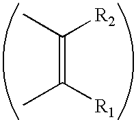
- M denotes Ir, Pt, Rh or Pd
- n is 2 or 3
- R 1 and R 2 independently denote a linear or branched alkyl group having 1-20 carbon atoms capable of including one or at least two non-neighboring methylene groups which can be replaced with —O—, —S—, —CO—, —CO—O—, —O—CO—, —CH ⁇ CH— or —C ⁇ C— and capable of including hydrogen atom which can be replaced with fluorine atom
- CyN denotes a cyclic group containing nitrogen atom connected to M and capable of having a substituent selected from the group consisting of halogen atom; nitro group; phenyl group; trialkylsilyl group having 1-8 carbon atoms; and a linear or branched alkyl group having 1-20 carbon atoms capable of including one or at least two non-neighboring methylene groups which can be replaced with —O—, —S—,
- the metal coordination compound of the present invention exhibits phosphorescence at the time of energy transfer from an excited state to a ground state to provide a high luminescence efficiency.
- an electrical device comprising: a substrate, a first electrode disposed on the substrate, an organic compound layer disposed on the first electrode, and a second electrode disposed on the organic compound layer, the organic compound layer comprising a metal coordination compound represented by the following formula (1):
- M denotes Ir, Pt, Rh or Pd
- n is 2 or 3
- R 1 and R 2 independently denote a linear or branched alkyl group having 1-20 carbon atoms capable of including one or at least two non-neighboring methylene groups which can be replaced with —O—, —S—, —CO—, —CO—O—, —O—CO—, —CH ⁇ CH— or —C ⁇ C— and capable of including hydrogen atom which can be replaced with fluorine atom
- CyN denotes a cyclic group containing nitrogen atom connected to M and capable of having a substituent selected from the group consisting of halogen atom; nitro group; phenyl group; trialkylsilyl group having 1-8 carbon atoms; and a linear or branched alkyl group having 1-20 carbon atoms capable of including one or at least two non-neighboring methylene groups which can be replaced with —O—, —S—,
- an image display apparatus including the organic luminescence device and voltage application means for applying a voltage to the organic luminescence device.
- FIGS. 1A, 1B and 1 C are respectively a schematic sectional view of a layer structure of an organic luminescence device.
- FIG. 2 is a schematic perspective view of an organic luminescence device (EL device) of a single matrix-type used in Example 13 appearing hereinafter.
- EL device organic luminescence device
- FIG. 3 is a waveform diagram of a driving signal employed in Example 13.
- a process of emission of light may generally involve the following steps:
- desired energy transmission and luminescence may generally be caused based on various quenching and competition.
- a luminescence center material per se is required to provide a higher yield of luminescence quantum.
- an efficient energy transfer between host material molecules and/or between host material molecule and guest material molecule is also an important factor.
- the above-described luminescent deterioration in energized state may presumably relate to the luminescent center material per se or an environmental change thereof by its ambient molecular structure.
- the metal coordination compound of formula (1) allows a high-efficiency luminescence with a high brightness (luminance) for a long period (i.e., a decreased luminescent deterioration in energized state).
- CyN may preferably be a cyclic group having a ring structure selected from the group consisting of pyridine, quinoline, imidazole, pyrazole, benzothiazole, benzoxazole, and benzimidazole, and capable of having said substituent. CyN may more preferably have a ring structure comprising pyridine or quinoline capable of having a substituent.
- the metal coordination compound represented by the above formula (1) according to the present invention causes phosphorescence (luminescence) and is assumed to have a lowest excited state comprising a triplet excited state liable to cause metal-to-ligand charge transfer (MLCT* state) or ⁇ * state.
- MLCT* state metal-to-ligand charge transfer
- ⁇ * state metal-to-ligand charge transfer
- the phosphorescent emission of light (phosphorescence) is caused to occur during the transition from the MLCT* state or ⁇ * state to the ground state.
- the metal coordination compound of formula (1) according to the present invention has been found to provide a higher phosphorescence yield of 0.15-0.9 and a shorter phosphorescence life of 1-40 psec.
- the shorter phosphorescence life is necessary to provide a resultant EL device with a higher luminescence efficiency. This is because the longer phosphorescence life increases molecules placed in their triplet excited state which is a waiting state for phosphorescence, thus lowering the resultant luminescence efficiency particularly at a higher current density.
- the metal coordination compound of formula (1) according to the present invention is a suitable luminescent material for an organic EL device with a higher phosphorescence yield and a shorter phosphorescence life.
- the metal coordination compound of formula (1) is suitable luminescent material for an organic EL device.
- results of photoluminescence of the phosphorescent material do not reflect luminescent characteristics of the resultant EL device in many cases since the luminescent characteristics in the case of the phosphorescent material depend on a magnitude of polarity of ambient host material molecules, ambient temperature, presence state of the material (e.g., solid state or liquid state), etc. Accordingly, different from the fluorescent material, it is generally difficult to expect the resultant EL characteristics for the phosphorescent material by simply removing a part of characteristics from results of photoluminescence characteristics.
- the metal coordination compound of formula (1) of the present invention exhibits an excellent stability. This may be attributable to an intermolecular interaction based on incorporation of the chain alkene group into the ligand of the metal coordination compound of formula (1). Specifically, an intermolecular interaction of molecules of the metal coordination compound of formula (1) with molecules of, e.g., the ambient host material is controlled by the incorporated chain alkene group, thus allowing suppression of formation of excited association structure causing thermal quenching (deactivation). As a result, quenching step is reduced thereby to improve the resultant device characteristics.
- the organic luminescence device of the present invention may preferably be an electric field-luminescence device as shown in FIGS. 1A to 1 C wherein a voltage is applied between a pair of electrodes sandwiching an organic (compound) layer containing the metal coordination compound of formula (1) to cause luminescence from the organic layer.
- the metal coordination compound of formula (1) according to the present invention may, e.g., be synthesized through the following reaction schemes.
- reaction mixture was cooled and subjected to extraction with cool water and ethyl acetate.
- the organic layer was washed with water, followed by distilling-off of the solvent under reduced pressure to obtain a residue.
- reaction mixture was poured into ice water and subjected to filtration with “Celite”.
- the organic layer was recovered from the filtrate and washed with water, followed by distilling-off of the solvent to obtain a residue.
- the reaction mixture was 20 cooled to room temperature.
- the resultant precipitate was recovered by filtration and successively washed with water, ethanol and acetone, followed by distilling-off of the solvent under reduced pressure at room temperature to obtain 0.53 g of 25 tetrakis[trans-2-(1-hexenyl)pyridine-C 2 , N] (u-dichloro)diiridium (III) (pale yellow powder) (Yield: 56.8%).
- the metal coordination compound of formula (1) (Ex. Comp. No. (13)) was dissolved in toluene to prepare a first solution and a second solution.
- the first solution was subjected to aeration with oxygen gas and the second solution was subjected to aeration with nitrogen gas.
- the oxygen-aerated solution exhibited substantially no photoluminescence but the nitrogen-aerated solution exhibited photoluminescence.
- the metal coordination compound of formula (1) of the present invention was found to be a phosphorescent metal coordination compound.
- the metal coordination compound was dissolved in chloroform and was spin-coated on a quartz substrate to form a ca. 0.1 ⁇ m-thick metal coordination compound layer.
- the above-prepared metal coordination compound layer formed on the substrate was subjected to pulse irradiation with nitrogen laser light (excitation wavelength: 337 nm) at room temperature to measure an attenuation time immediately after the excitation laser pulse irradiation.
- nitrogen laser light excitation wavelength: 337 nm
- a luminescence intensity I after a lapse of t (sec) is defined as the following equation:
- I 0 represents an initial luminescence intensity and ⁇ (psec) represents a luminescence life (time).
- the metal coordination compound of formula (1) (Ex. Comp. No. (13)) showed a shorter luminescence life of at most 10 psec. among ordinary luminescent materials.
- metal coordination compound of formula (1) of the present invention may include those shown in Table 1 below.
- the metal coordination compound of the present invention is, however, not restricted to these examples.
- Each of the organic luminescence devices had a structure including three organic (compound) layers (luminescence function layers) shown in FIG. 1B.
- a 100 nm-thick film (transparent electrode 14) of ITO indium tin oxide was formed by sputtering, followed by patterning to have an (opposing) electrode area of 3 mm
- ITO indium tin oxide
- three organic layers and two metal electrode layers shown below were successively formed by vacuum (vapor) deposition using resistance heating in a vacuum chamber (10 ⁇ 4 Pa).
- Organic layer 1 (hole transport layer 13) (40 nm): ⁇ -NPD
- Organic layer 2 (luminescence layer 12) (30 nm): CBP/metal coordination compound of formula (1) shown in Table 2 (95/5 by weight) (co-vacuum deposition)
- Organic layer 3 (electron transport layer 16) (30 nm): Alq3
- Metal electrode layer 2 (metal electrode 11) (100 nm): Al
- EL characteristics of the luminescence devices using the metal coordination compounds of formula (1) were measured by using a microammeter (“Model 4140B”, mfd. by Hewlett-Packard Co.) for a current density under application of a voltage of 12 volts (current-voltage characteristic) and using a luminance meter (“Model-BM7”, mfd. by Topcon K.K.) for a luminescence luminance at room temperature. Further, both the above-prepared luminescence devices showed a good rectification characteristic.
- each of the above-prepared luminescence devices was taken out of the vacuum chamber and was subjected to a continuous energization test in an atmosphere of dry nitrogen gas stream so as to remove device deterioration factors, such as oxygen and moisture (water content).
- the continuous energization test was performed by continuously applying a drive voltage waveform shown in FIG. 3 at a constant current density of 70 mA/cm 2 to the luminescence device having the ITO (transparent) electrode (as an anode) and the Al (metal) electrode (as a cathode), followed by measurement of luminance (brightness) with time so as to determine a time (luminance half-life) required for decreasing an initial luminance (60-220 cd/m 2 ) to 1 ⁇ 2 thereof.
- the luminescence devices using the ordination compounds of formula (1) according to the present invention provide longer luminance half-lives, thus resulting in an EL device having a high durability (luminance stability) based on a good stability of the metal coordination compound of formula (1) of the present invention.
- a simple matrix-type organic EL device shown in FIG. 2 was prepared in the following manner.
- a ca. 100 nm-thick transparent electrode 22 of ITO (as an anode) was formed by sputtering, followed by patterning in a stripe form comprising 100 lines (each having a width of 100 ⁇ m and a spacing of 40 ⁇ m).
- an organic lamination layer 23 including three organic layers was formed in the same manner as in Example 1 (using the metal coordination compound of formula (1) (Ex. Comp. No. (5)).
- the thus-prepared organic EL device was placed in a glove box aerated with nitrogen gas and driven in a simple matrix manner (frame frequency: 30 Hz,interlace scanning) by applying a driving waveform (drive voltage: 7 to 13 volts, scanning signal voltage: 10 volts, data signal voltage: ⁇ 3 volts) as shown in FIG. 3.
- driving waveform drive voltage: 7 to 13 volts, scanning signal voltage: 10 volts, data signal voltage: ⁇ 3 volts
- the organic luminescence device of the present invention may be applicable to flat panel displays based on its high-efficiency luminescence characteristics. As a result, it becomes possible to provide a flat panel display device having advantages, such as a good energy saving performance, high visibility and light weight properties.
- the organic luminescence device of the present invention When the organic luminescence device of the present invention is used as a light source for a printer, for example, the organic luminescence device is formed in a line form and disposed in proximity to a photosensitive drum, thus allowing independent drive of respective device elements as a line shutter to effect desired exposure to the photosensitive drum. Further, when the organic luminescence device of the present invention is used as an illumination device or a backlight for a liquid crystal display apparatus, compared with the case of an ordinary fluorescent lamp, the organic luminescence device is expected to exhibit an excellent energy saving effect.
- the organic luminescence device of the present invention may particularly suitably be employed in an image forming display apparatus of an active matrix-type including TFTs (thin film transistors).
- a metal coordination compound of formula (1) exhibiting a higher phosphorescence yield and a shorter phosphorescence life (time) and allowing control of a maximum luminescence wavelength based on a combination of a chain alkene group and an N-containing cyclic group (CyN).
- the metal coordination compound of formula (1) is used as an organic (compound) layer of an organic luminescence device, the resultant organic luminescence device exhibits not only a high-efficiency luminescence but also a high luminance for a long period of time while suppressing a deterioration in luminescence in energized state.
Landscapes
- Chemical & Material Sciences (AREA)
- Organic Chemistry (AREA)
- Crystallography & Structural Chemistry (AREA)
- Inorganic Chemistry (AREA)
- Engineering & Computer Science (AREA)
- Materials Engineering (AREA)
- Electroluminescent Light Sources (AREA)
Abstract
A metal coordination compound suitable as an organic material for a luminescent device is represented by the following formula (1):

wherein M denotes Ir, Pt, Rh or Pd; n is 2 or 3; R1 and R2 independently denote a linear or branched alkyl group having 1-20 carbon atoms capable of including one or at least two non-neighboring methylene groups which can be replaced with —O—, —S—, —CO—, —CO—O—, —O—CO—, —CH═CH— or —C≡C— and capable of including hydrogen atom which can be replaced with fluorine atom; and CyN denotes a cyclic group containing nitrogen atom connected to M and capable of having a substituent selected from the group consisting of halogen atom; nitro group; phenyl group; trialkylsilyl group having 1-8 carbon atoms; and a linear or branched alkyl group having 1-20 carbon atoms capable of including one or at least two non-neighboring methylene groups which can be replaced with —O—, —S—, —CO—, —CO—O—, —O—CO—, —CH═CH— or —C≡C— and capable of including hydrogen atom which can be replaced with fluorine atom.
Description
- The present invention relates to a metal coordination compound, an electrical device using the metal coordination compound and a display apparatus using the device. More specifically, the present invention relates to an organic metal coordination compound having a formula (1) appearing hereinafter as a luminescence material so as to allow high luminance for a long period of time, an organic luminescence device using the metal coordination compound and a display apparatus including the luminescence device.
- An organic electroluminescence (EL) device has been extensively studied as a luminescence device with a high responsiveness and high efficiency.
- The organic EL device generally has a sectional structure as shown in FIG. 1A or 1B (e.g., as described in “Macromol. Symp.”, 125, pp. 1-48 (1997)).
- Referring to the figures, the EL device generally has a structure including a
transparent substrate 15, atransparent electrode 14 disposed on thetransparent substrate 15, ametal electrode 11 disposed opposite to thetransparent electrode 14, and a plurality of organic (compound) layers, as luminescence function layers, disposed between thetransparent electrode 14 and themetal electrode 11. - Referring to FIG. 1A, the EL device in this embodiment has two organic layers including a
luminescence layer 12 and ahole transport layer 13. - The
transparent electrode 14 may be formed of a film of ITO (indium tin oxide) having a larger work function to ensure a good hole injection performance into the hole transport layer. On the other hand, themetal electrode 11 may be formed of a layer of aluminum, magnesium, alloys thereof, etc., having a smaller work function to ensure a good electron injection performance into the organic layer(s). - These (transparent and metal)
electrodes - The
luminescence layer 12 may be formed of, e.g., aluminum quinolinol complex (representative example thereof may include Alq3 described hereinafter) having an electron transporting characteristic and a luminescent characteristic. Thehole transport layer 13 may be formed of, e.g., biphenyldiamine derivative (representative example thereof may include α-NPD described hereinafter) having an electron donating characteristic. - The above-described EL device exhibits a rectification characteristic, so that when an electric field is applied between the
metal electrode 11 as a cathode and thetransparent electrode 14 as an anode, electrons are injected from themetal electrode 11 into theluminescence layer 12 and holes are injected from thetransparent electrodes 14. - The thus-injected holes and electrons are recombined within the
luminescence layer 12 to produce excitons placed in an excited state, thus causing luminescence at the time of transition of the excitons to a ground state. At that time, thehole transport layer 13 functions as an electron-blocking layer to increase a recombination efficiency at the boundary between theluminescence layer 12 and thehole transport layer 13, thus enhancing a luminescence efficiency. - Referring to FIG. 1B, in addition to the layers shown in FIG. 1A, an
electron transport layer 16 is disposed between themetal electrode 11 and theluminescence layer 12, whereby an effective carrier blocking performance can be ensured by separating functions of luminescence, electron transport and hole transport, thus allowing effective luminescence. - The
electron transport layer 16 may be formed of, e.g., oxadiazole derivatives. - In ordinary organic EL devices, fluorescence caused during a transition of luminescent center molecule from a singlet excited state to a ground state is used as luminescence.
- On the other hand, different from the above fluorescence (luminescence) via singlet exciton, phosphorescence (luminescence) via triplet exciton has been studied for use in organic EL device as described in, e.g., “Improved energy transfer in electrophosphorescent device” (D. F. O'Brien et al., Applied Physics Letters, Vol. 74, No. 3, pp. 442-444 (1999)) and “Very high-efficiency green organic light-emitting devices based on electrophosphorescence” (M. A. Baldo et al., Applied Physics Letters, Vol. 75, No. 1, pp. 4-6 (1999)).
- The EL devices shown in these documents may generally have a sectional structure shown in FIG. 1C.
- Referring to FIG. 1C, four organic layers including a
hole transfer layer 13, aluminescence layer 12, an exciton diffusion-prevention layer 17, and anelectron transport layer 16 are successively formed in this order on the transparent electrode (anode) 14. - In the above documents, higher efficiencies have been achieved by using four organic layers including a
hole transport layer 13 of α-NPD (shown below), anelectron transport layer 16 of Alq3 (shown below), an exciton diffusion-prevention layer 17 of BPC (shown below), and aluminescence layer 12 of a mixture of CPB (shown below) as a host material with Ir(ppy)3 (shown below) or PtOEP (shown below) as a guest phosphorescence material doped into CBP at a concentration of ca. 6 wt. %.
- Alq3: tris(8-hydroxyquinoline) aluminum (aluminum-quinolinol complex),
- α-NPD: N4,N4′-di-naphthalene-1-yl-N4,N4′-diphenyl-biphenyl-4,4′-diamine (4,4′-bis[N-(1-naphthyl)-N-phenyl-amino]biphenyl),
- CBP: 4,4′-N,N′-dicarbazole-biphenyl,
- BCP: 2,9-dimethyl-4,7-diphenyl-1,10-phenanthroline,
- Ir(ppy) 3: fac tris(2-phenylpyridine)iridium (iridium-phenylpyridine complex), and
- PtOEP: 2,3,7,8,12,13,17,18-octaethyl-21H,23H-porphine platinum (platinum-octaethyl porphine complex).
- The phosphorescence (luminescence) material used in the
luminescence layer 12 has particularly attracted notice. This is because the phosphorescence material is expected to provide a higher luminescence efficiency in principle. - More specifically, in the case of the phosphorescence material, excitons produced by recombination of carriers comprise singlet excitons and triplet excitons presented in a ratio of 1:3. For this reason, when fluorescence caused during the transition from the singlet excited state to the ground state is utilized, a resultant luminescence efficiency is 25% (as upper limit) based on all the produced excitons in principle.
- On the other hand, in the case of utilizing phosphorescence caused during transition from the triplet excited state, a resultant luminescence efficiency is expected to be at least three times that of the case of fluorescence in principle. In addition thereto, if intersystem crossing from the singlet excited state (higher energy level) to the triplet excited state is taken into consideration, the luminescence efficiency of phosphorescence can be expected to be 100% (four times that of fluorescence) in principle.
- The use of phosphorescence based on transition from the triplet excited state has also been proposed in, e.g., Japanese Laid-Open Patent Application (JP-A) 11-329739, JP-A 11-256148 and JP-A 8-319482.
- However, the above-mentioned organic EL devices utilizing phosphorescence have accompanied with problems of a lower luminescence efficiency and stability thereof (luminescent deterioration) particularly in an energized state.
- The reason for luminescent deterioration has not been clarified as yet but may be attributable to such a phenomenon that the life of triplet exciton is generally longer than that of singlet exciton by at least three digits, so that molecule is placed in a higher-energy state for a long period to cause reaction with ambient substance, formation of exciplex or excimer, change in minute molecular structure, structural change of ambient substance, etc.
- Accordingly, the (electro)phosphorescence EL device is expected to provide a higher luminescence efficiency as described above, while the EL device is required to suppress or minimize the luminescent deterioration in energized state affecting the life of the EL device.
- An object of the present invention is to provide a metal coordination compound as a material suitable for an organic layer for a luminescence device (as an electrical device) capable of providing a high-efficiency luminescent state at a high brightness (or luminance) for a long period while minimizing the deterioration in luminescence in energized state.
- Another object of the present invention is to provide an organic luminescence device including the metal coordination compound.
- A further object of the present invention is to provide a display apparatus including the organic luminescence device.
- According to the present invention, there is provided a metal coordination compound represented by the following formula (1):

- wherein M denotes Ir, Pt, Rh or Pd; n is 2 or 3; R 1 and R2 independently denote a linear or branched alkyl group having 1-20 carbon atoms capable of including one or at least two non-neighboring methylene groups which can be replaced with —O—, —S—, —CO—, —CO—O—, —O—CO—, —CH═CH— or —C≡C— and capable of including hydrogen atom which can be replaced with fluorine atom; and CyN denotes a cyclic group containing nitrogen atom connected to M and capable of having a substituent selected from the group consisting of halogen atom; nitro group; phenyl group; trialkylsilyl group having 1-8 carbon atoms; and a linear or branched alkyl group having 1-20 carbon atoms capable of including one or at least two non-neighboring methylene groups which can be replaced with —O—, —S—, —CO—, —CO—O—, —O—CO—, —CH═CH— or —C≡C— and capable of including hydrogen atom which can be replaced with fluorine atom.
- The metal coordination compound of the present invention exhibits phosphorescence at the time of energy transfer from an excited state to a ground state to provide a high luminescence efficiency.
- According to the present invention, there is also provided an electrical device, comprising: a substrate, a first electrode disposed on the substrate, an organic compound layer disposed on the first electrode, and a second electrode disposed on the organic compound layer, the organic compound layer comprising a metal coordination compound represented by the following formula (1):

- wherein M denotes Ir, Pt, Rh or Pd; n is 2 or 3; R 1 and R2 independently denote a linear or branched alkyl group having 1-20 carbon atoms capable of including one or at least two non-neighboring methylene groups which can be replaced with —O—, —S—, —CO—, —CO—O—, —O—CO—, —CH═CH— or —C≡C— and capable of including hydrogen atom which can be replaced with fluorine atom; and CyN denotes a cyclic group containing nitrogen atom connected to M and capable of having a substituent selected from the group consisting of halogen atom; nitro group; phenyl group; trialkylsilyl group having 1-8 carbon atoms; and a linear or branched alkyl group having 1-20 carbon atoms capable of including one or at least two non-neighboring methylene groups which can be replaced with —O—, —S—, —CO—, —CO—O—, —O—CO—, —CH═CH— or —C□C— and capable of including hydrogen atom which can be replaced with fluorine atom.
- By applying a voltage between the pair of electrodes of the organic luminescence device to cause phosphorescence from the organic compound layer (luminescence function layer) containing the metal coordination compound.
- According to the present invention, there is further provided an image display apparatus including the organic luminescence device and voltage application means for applying a voltage to the organic luminescence device.
- These and other objects, features and advantages of the present invention will become more apparent upon a consideration of the following description of the preferred embodiments of the present invention taken in conjunction with the accompanying drawings.
- FIGS. 1A, 1B and 1C are respectively a schematic sectional view of a layer structure of an organic luminescence device.
- FIG. 2 is a schematic perspective view of an organic luminescence device (EL device) of a single matrix-type used in Example 13 appearing hereinafter.
- FIG. 3 is a waveform diagram of a driving signal employed in Example 13.
- In the case where a luminescence layer for an organic EL device is formed of a carrier transporting host material and a phosphorescent guest material, a process of emission of light (phosphorescence) may generally involve the following steps:
- (1) transport of electron and hole within a luminescence layer,
- (2) formation of exciton of the host material,
- (3) transmission of excited energy between host material molecules,
- (4) transmission of excited energy from the host material molecule to the guest material molecule,
- (5) formation of triplet exciton of the guest material, and
- (6) emission of light (phosphorescence) caused during transition from the triplet excited state to the ground state of the guest material.
- In the above steps, desired energy transmission and luminescence may generally be caused based on various quenching and competition.
- In order to improve a luminescence efficiency of the EL device, a luminescence center material per se is required to provide a higher yield of luminescence quantum. In addition thereto, an efficient energy transfer between host material molecules and/or between host material molecule and guest material molecule is also an important factor.
- Further, the above-described luminescent deterioration in energized state may presumably relate to the luminescent center material per se or an environmental change thereof by its ambient molecular structure.
- For this reason, our research group has extensively investigated an effect of use of the metal coordination compound of formula (1) as the luminescent center material and as a result, has found that the metal coordination compound of formula (1) allows a high-efficiency luminescence with a high brightness (luminance) for a long period (i.e., a decreased luminescent deterioration in energized state).
- In the formula (1) for the metal coordination compound of the present invention, CyN may preferably be a cyclic group having a ring structure selected from the group consisting of pyridine, quinoline, imidazole, pyrazole, benzothiazole, benzoxazole, and benzimidazole, and capable of having said substituent. CyN may more preferably have a ring structure comprising pyridine or quinoline capable of having a substituent.
- The metal coordination compound represented by the above formula (1) according to the present invention causes phosphorescence (luminescence) and is assumed to have a lowest excited state comprising a triplet excited state liable to cause metal-to-ligand charge transfer (MLCT* state) or ρ−π* state. The phosphorescent emission of light (phosphorescence) is caused to occur during the transition from the MLCT* state or π−π* state to the ground state.
- The metal coordination compound of formula (1) according to the present invention has been found to provide a higher phosphorescence yield of 0.15-0.9 and a shorter phosphorescence life of 1-40 psec.
- The shorter phosphorescence life is necessary to provide a resultant EL device with a higher luminescence efficiency. This is because the longer phosphorescence life increases molecules placed in their triplet excited state which is a waiting state for phosphorescence, thus lowering the resultant luminescence efficiency particularly at a higher current density.
- Accordingly, the metal coordination compound of formula (1) according to the present invention is a suitable luminescent material for an organic EL device with a higher phosphorescence yield and a shorter phosphorescence life.
- Further, by appropriately selecting a combination of the chain alkene group
- and the N-containing cyclic group (CyN) constituting the metal coordination compound of formula (1), it is possible to expect a controlled luminescence wavelength ranging from a shorter wavelength to a longer wavelength. Also from this viewpoint, the metal coordination compound of formula (1) of the present invention is suitable luminescent material for an organic EL device.
- In the case of phosphorescent (luminescent) material, luminescent characteristics are largely affected by its molecular environment. On the other hand, principal characteristics of the fluorescent material are studied based on photoluminescence.
- For this reason, results of photoluminescence of the phosphorescent material do not reflect luminescent characteristics of the resultant EL device in many cases since the luminescent characteristics in the case of the phosphorescent material depend on a magnitude of polarity of ambient host material molecules, ambient temperature, presence state of the material (e.g., solid state or liquid state), etc. Accordingly, different from the fluorescent material, it is generally difficult to expect the resultant EL characteristics for the phosphorescent material by simply removing a part of characteristics from results of photoluminescence characteristics.
- Further, as substantiated in Examples appearing hereinafter, it has been clarified that the metal coordination compound of formula (1) of the present invention exhibits an excellent stability. This may be attributable to an intermolecular interaction based on incorporation of the chain alkene group into the ligand of the metal coordination compound of formula (1). Specifically, an intermolecular interaction of molecules of the metal coordination compound of formula (1) with molecules of, e.g., the ambient host material is controlled by the incorporated chain alkene group, thus allowing suppression of formation of excited association structure causing thermal quenching (deactivation). As a result, quenching step is reduced thereby to improve the resultant device characteristics.
- The organic luminescence device of the present invention may preferably be an electric field-luminescence device as shown in FIGS. 1A to 1C wherein a voltage is applied between a pair of electrodes sandwiching an organic (compound) layer containing the metal coordination compound of formula (1) to cause luminescence from the organic layer.
- The metal coordination compound of formula (1) according to the present invention may, e.g., be synthesized through the following reaction schemes.
- <Synthesis of Ligand L>
- 1) case of R 1=H

- 2) case of R 1=alkyl, R2=alkyl

- <Synthesis of Ir Complex>

- Step (i)

- In a 2 liter-three-necked flask, 105.6 g (668 mM) of 2-bromopyridine, 61.8 g (735 mM) of 2-methyl-3-buthine-2-ol, 2.8 g (11 mM) of triphenylphosphine, 1.46 g (2.08 mM) of bis(triphenylphosphine) palladium (II) dichloride, and 620 ml of triethylamine were placed and stirred on an ice bath in a nitrogen gas stream atmosphere, followed by addition thereto of 0.46 g (2.42 mM) of copper iodide, stirring for 1.5 hours at room temperature, and refluxing for 5.5 hours under stirring.
- After the reaction, the reaction mixture was cooled and subjected to extraction with cool water and ethyl acetate. The organic layer was washed with water, followed by distilling-off of the solvent under reduced pressure to obtain a residue. The residue was purified by silica gel column chromatogaphy (eluent: toluene/THF (tetrahydrofuran)=10/1) to obtain 86.9 g of liquid 2-methyl-2-hydroxy-4-(2-pyridyl)-3-buthine (Yield: 80.6%).
- In a 2 liter-three-necked flask, 86.5 g (537 mM) of 2-methyl-2-hydroxy-4-(2-pyridyl)-3-buthine and 1100 ml of dry toluene were placed. To the mixture, 2.14 g (53.6 mM) of oily sodium hydride was intermittently added (fine times in total), followed by stirring for 0.5 hour at room temperature. On an oil bath, the system was gradually heated to distill off formed acetone, and the inner temperature was increased up to 105° C.
- After the reaction, the reaction mixture was cooled and poured into water, followed by extraction with toluene. The organic layer was washed with water, and the solvent was distilled off under reduced pressure to obtain a residue. The residue was purified by silica gel column chromatography (eluent: hexane/methyl t-butyl ether=5/1) to obtain 32.9 g of liquid 2-ethynypyridine (Yield: 59.5%).
- Step (ii)

- In a 2 liter-three-necked flask, 32.8 g (318 mM) of 2-ethynylpyridine and 330 ml of dry THF were placed and cooled on an ice-common salt bath in a nitrogen gas stream atmosphere. At −12 to −4° C., 239 ml of 1.6M-butylithium solution in THF was added dropwise to the mixture, followed by stirring for 2 hours at −12 to −10° C. At that temperature, to the resultant mixture, 115 ml of HMPA (hexamethylphosphoramide) was added dropwise, followed by stirring for 5 min. at that temperature and further dropwise addition thereto of 70.3 (382 mM) of 1-iodobutane, whereby the inner temperature of the system was increased from −11° C. to −3° C. and then was further gradually increased to 3° C. after 4 hours from the addition.
- The reaction mixture was left standing overnight at room temperature and poured into ice water, followed by extraction with toluene. The organic layer was washed with water, followed by distilling-off of the solvent under reduced pressure to obtain a residue. The residue was purified by silica gel column chromatography (eluent: toluene) to obtain 17.6 g of liquid 2-(1-hexynyl)pyridine (Yield: 34.8%).
- In a 1 liter-three-necked flask, 15.1 g (389 mM) of lithium aluminum hydride and 320 ml of ether were placed and cooled on an ice bath in a nitrogen gas atmosphere, followed by dropwise addition thereto of a solution of 15.8 g (99.2 mM) of 2-(1-hexynyl)pyridine in 160 ml of ether at −11° C. After the addition, the mixture was stirred for 0.5 hour at that temperature, and then was gradually heated, followed by refluxing for 5 hours under stirring.
- After the reaction, the reaction mixture was poured into ice water and subjected to filtration with “Celite”. The organic layer was recovered from the filtrate and washed with water, followed by distilling-off of the solvent to obtain a residue. The residue was purified by silica gel column chromatography (eluent: toluene/THF=100/1) to obtain 4.80 g of liquid trans-2-(1-hexenyl)pyridine (Yield: 31.4%).
- Step (iii)

- In a 200 ml-three-necked flask, 0.60 g (1.70 mM) of iridium (III) chloride, 1.23 g (7.63 mM) of trans-2-(1-hexenyl)pyridine, 50 ml of
ethoxyethanol 15 and 20 ml of water were placed and stirred for 0.5 hour at room temperature in a nitrogen gas stream atmosphere, followed by refluxing for 24 hours under stirring. - After the reaction, the reaction mixture was 20 cooled to room temperature. The resultant precipitate was recovered by filtration and successively washed with water, ethanol and acetone, followed by distilling-off of the solvent under reduced pressure at room temperature to obtain 0.53 g of 25 tetrakis[trans-2-(1-hexenyl)pyridine-C 2, N] (u-dichloro)diiridium (III) (pale yellow powder) (Yield: 56.8%).
- Step (iv)

- In a 100 ml-three-necked flask, 50 ml of ethoxyethanol, 0.52 g (0.47 mM) of tetrakis[trans-2-(1-hexenyl)pyridino-C 2,N] (p-dichloro)diiridium (III), 0.15 g (1.50 mM) of acetylacetone and 0.71 g (6.70 mM) of sodium carbonate were placed and stirred at room temperature in a nitrogen gas stream atmosphere, followed by refluxing for 15 hours under stirring.
- After the reaction, the reaction mixture was cooled on an ice bath. The resultant precipitate was recovered by filtration and washed with water. The resultant precipitate was purified by silica gel column chromatography (eluent: chloroform/methanol =30/1) to obtain 0.22 g of bis[trans-2-(1-hexenyl)pyridine-C 2,N] (acetylacetonato)iridium (III) (pale yellow powder) (Yield: 37.9%).
- Step (v)

- In a 100 ml-three-necked flask, 0.21 g (0.34 mM) of bis[trans-2-(1-hexenyl)pyridine-C 2,N] (acetylacetonato)iridium (III), 0.12 g (0.74 mM) of trans-2-(1-hexenyl)pyridine and 25 ml of glycerol were placed and stirred for 8 hours at ca. 180° C. in a nitrogen gas stream atmosphere.
- After the reaction, the reaction mixture cooled to room temperature was poured into 170 ml of 1N-hydrochloric acid. The resultant precipitate was recovered by filtration, washed with water and dried for 5 hour at 100° C. under reduced pressure. The resultant dried residue was purified by silica gel column chromatography (eluent: chloroform) to obtain 0.10 g of tris[trans-2-(1-hexenyl)pyridine-C 2 N]iridium (III) (Ex. Comp. No. (13); pale yellow powder) (Yield: 43.3%).
- The thus-obtained metal coordination compound of formula (1) (Ex. Comp. No. (13)) was then subjected to MALDI-TOF MS (matrix-assisted laser desorption ionization-time of flight mass spectrometry), whereby it was confirmed that the metal coordination compound has M + of 672.9.
- In order to confirm that the luminescence was phosphorescence, the metal coordination compound of formula (1) (Ex. Comp. No. (13)) was dissolved in toluene to prepare a first solution and a second solution. The first solution was subjected to aeration with oxygen gas and the second solution was subjected to aeration with nitrogen gas.
- When the thus-prepared first and second solutions were subjected to light irradiation, the oxygen-aerated solution exhibited substantially no photoluminescence but the nitrogen-aerated solution exhibited photoluminescence. As a result, the metal coordination compound of formula (1) of the present invention was found to be a phosphorescent metal coordination compound.
- The metal coordination compound of formula (1) (Ex. Comp. No. (13)) was then subjected to measurement of luminescence life (time) in the following manner.
- The metal coordination compound was dissolved in chloroform and was spin-coated on a quartz substrate to form a ca. 0.1 μm-thick metal coordination compound layer.
- By using a luminescence life-measuring apparatus (available from Hamamatsu Photonics K.K.), the above-prepared metal coordination compound layer formed on the substrate was subjected to pulse irradiation with nitrogen laser light (excitation wavelength: 337 nm) at room temperature to measure an attenuation time immediately after the excitation laser pulse irradiation.
- A luminescence intensity I after a lapse of t (sec) is defined as the following equation:
- I=I 0 exp(−t/τ),
- wherein I 0 represents an initial luminescence intensity and τ (psec) represents a luminescence life (time).
- As a result, the metal coordination compound of formula (1) (Ex. Comp. No. (13)) showed a shorter luminescence life of at most 10 psec. among ordinary luminescent materials.
- Other metal coordination compounds of formula (1) of the present invention may be principally synthesized in a similar manner as in Synthesis Example described above.
- Specific examples of the metal coordination compound of formula (1) of the present invention may include those shown in Table 1 below. The metal coordination compound of the present invention is, however, not restricted to these examples.
- In Table 1, symbols Pr to Bi represent the following divalent groups, respectively.

TABLE 1 No. M n R1 R2 CyN X1 X2 X3 (1) Ir 3 H H Pr H H — (2) Ir 3 H CH3 Pr H H — (3) Ir 3 H CH3 Pr OCH3 H — (4) Ir 3 H CH3 Pr H CF3 — (5) Ir 3 H C2H5 Pr H H — (6) Ir 3 H C2H5 Pr H OCH2C≡CCH3 — (7) Ir 3 H C2H5 Pr C3F7 H — (8) Ir 3 H C3H7 Pr H H — (9) Ir 3 H C3H7 Pr H CF3 — (10) Ir 3 H C3H7 Pr H Cl — (11) Ir 3 H C3H7 Pr CF3 H — (12) Ir 3 H C3H7 Pr CF3 CF3 — (13) Ir 3 H C4H9 Pr H H — (14) Ir 3 H C4H9 Pr OCH3 H — (15) Ir 3 H C4H9 Pr H CF3 — (16) Ir 3 H C4H9 Pr OC4H9 H — (17) Ir 3 H C4H9 Pr NO2 H — (18) Ir 3 H C4H9 Pr CF3 H — (19) Ir 3 H C4H9 Pr CF3 CF3 — (20) Ir 3 H C4H9 Pr H OCH(CH3)2 — (21) Ir 3 H C4H9 Pr H C5F11 — (22) Ir 3 H C4H9 Pr H Si(CH3)2C4H9 — (23) Ir 3 H C5H11 Pr H H — (24) Ir 3 H C5H11 Pr OCH3 H — (25) Ir 3 H C5H11 Pr Si(CH3)2C8H17 H — (26) Ir 3 H C5H11 Pr H Br — (27) Ir 3 H C5H11 Pr H COCH3 — (28) Ir 3 H C6H13 Pr H CF3 — (29) Ir 3 H C6H13 Pr H NO2 — (30) Ir 3 H C7H15 Pr H H — (31) Ir 3 H C8H17 Pr H H — (32) Ir 3 H C8H17 Pr H Cl — (33) Ir 3 H C8H17 Pr OC8H17 H — (34) Ir 3 H C15H21 Pr H H — (35) Ir 3 H C20H41 Pr H H — (36) Ir 3 H CH3O(CH2)6 Pr H H — (37) Ir 3 H C2H5(CH3)CH(CH2)4 Pr H H — (38) Ir 3 H C2H5C≡C(CH2)3 Pr H H — (39) Ir 3 H CH3CH═CH(CH2)7 Pr H H — (40) Ir 3 H (CH3)2CH(CH2)3 Pr H H — (41) Ir 3 H C3H7O(CH3)CHCH2O(CH2)2 Pr H H — (42) Ir 3 H CH3S(CH2)6 Pr H H — (43) Ir 3 H C2F5(CH2)6 Pr H CF3 — (44) Ir 3 H C3F7CH2O(CH2)2 Pr H H — (45) Ir 3 H CH3COO(CH2)4 Pr H H — (46) Ir 3 CH3 H Pr H H — (47) Ir 3 CH3 C3H7 Pr H H — (48) Ir 3 C2H5 C4H9 Pr H H — (49) Ir 3 C5H11O(CH2)3 C8H17 Pr H H — (50) Ir 3 C2F5(CH2)6 H Pr H H — (51) Ir 3 H H Q H H H (52) Ir 3 H CH3 Q H H H (53) Ir 3 H C4H9 Q H H H (54) Ir 3 H C4H9 Q H H OCH3 (55) Ir 3 H C8H17 Q H H Cl (56) Ir 3 C5H11 C12H25 Q H H H (57) Ir 3 H H Iz H H OC8H17 (58) Ir 3 H C4H9 Iz H H H (59) Ir 3 H C4H9 Pz H SC2H5 H (60) Ir 3 H C9H19 Pz H H H (61) Ir 3 H H Bz H H OCH(CH3)2 (62) Ir 3 H CH3 Bz H H H (63) Ir 3 H C3H7 Bz H H H (64) Ir 3 H C4H9 Bz H H H (65) Ir 3 H C4H9 Bz Cl H H (66) Ir 3 H C10H21 Bz H OC≡CC4H9 H (67) Ir 3 CH3 C2F5(CH2)6 Bz H H H (68) Ir 3 C3H7O(CH2)5 H Bz H H H (69) Ir 3 H C3H7 Bo H H COCH3 (70) Ir 3 H C4H9 Bo H H H (71) Ir 3 H C6H13 Bo H H H (72) Ir 3 H C7H15 Bo H H H (73) Ir 3 H C8H17 Bo H H C12H25 (74) Ir 3 H C13H27 Bo H Si(CH3)3 H (75) Ir 3 H C3H7O(CH3)CHCH2O(CH2)2 Bo H H OCH2C4F9 (76) Ir 3 C5H11 H Bo H H H (77) Ir 3 H C2H5 Bi H H H (78) Ir 3 H C4H9 Bi H H OCH3 (79) Ir 3 H C8H17 Bi H H Br (80) Ir 3 CH3 C10H21 Bi H H H (81) Pt 2 H H Pr H H — (82) Pt 2 H C2H5 Pr H H — (83) Pt 2 H C4H9 Pr H H — (84) Pt 2 H C4H9 Pr H CF3 — (85) Pt 2 H C5H11 Pr H H — (86) Pt 2 H C6H13 Pr H NO2 — (87) Pt 2 H C7H15 Pr H H — (88) Pt 2 H C8H17 Pr H H — (89) Pt 2 H C10H21 Pr OCH3 H — (90) Pt 2 H C14H29 Pr H Si(CH3)2C8H17 — (91) Pt 2 H C20H41 Pr H H — (92) Pt 2 H C2H5(CH3)CH(CH2)4 Pr H H — (93) Pt 2 H C2H5C≡C(CH2)3 Pr H H — (94) Pt 2 CH3 H Pr CF3 H — (95) Pt 2 C2F5(CH2)6 C3H7 Pr H H — (96) Pt 2 H C4H9 Q H H H (97) Pt 2 H CH3S(CH2)6 Q H H OCH3 (98) Pt 2 C5H11 H Iz H H H (99) Pt 2 H C6H13 Pz H H H (100) Pt 2 H C8H17 Bz H H H (101) Pt 2 H C12H25 Bz H H OCH(CH3)2 (102) Pt 2 H C4H9 Bo H H H (103) Pt 2 C5H11 C5H11 Bo H OCH2CH═CH2 H (104) Pt 2 H C9H19 Bi H H H (105) Rh 3 H H Pr H H — (106) Rh 3 H CH3 Pr H CF3 — (107) Rh 3 H C2H5 Pr H H — (108) Rh 3 H C4H9 Pr H H — (109) Rh 3 H C4H9 Pr OCH3 H — (110) Rh 3 H C4H9 Pr H CF3 — (111) Rh 3 H C4H9 Pr OC4H9 H — (112) Rh 3 H C4H9 Pr H Cl — (113) Rh 3 H C4H9 Pr CF3 CF3 — (114) Rh 3 H C4H9 Pr H NO2 — (115) Rh 3 H C5H11 Pr CF3 CF3 — (116) Rh 3 H C6H13 Pr H H — (117) Rh 3 H C6H13 Pr CF3 H — (118) Rh 3 H C7H15 Pr H OCH(CH3)2 — (119) Rh 3 H C8H17 Pr H H — (120) Rh 3 H C10H21 Pr H C5F11 — (121) Rh 3 H C14H29 Pr Si(CH3)2C8H17 H — (122) Rh 3 H C20H41 Pr H H — (123) Rh 3 H CH3O(CH2)6 Pr H H — (124) Rh 3 H C2H5(CH3)CH(CH2)4 Pr H H — (125) Rh 3 H C2H5C≡C(CH2)3 Pr H H — (126) Rh 3 H CH3CH═CH(CH2)7 Pr H H — (127) Rh 3 H C3H7O(CH3)CHCH2O(CH2)2 Pr H Cl — (128) Rh 3 H CH3S(CH2)6 Pr H H — (129) Rh 3 H C2F5(CH2)6 Pr H H — (130) Rh 3 H C3F7CH2O(CH2)2 Pr H H — (131) Rh 3 H CH3COO(CH2)4 Pr H H — (132) Rh 3 CH3 C3H7 Pr H H — (133) Rh 3 C2H5 C4H9 Pr H H — (134) Rh 3 C3H7O(CH2)5 H Pr H H — (135) Rh 3 H CH3 Q H H H (136) Rh 3 H C4H9 Q H H OCH3 (137) Rh 3 H C8H17 Q H H H (138) Rh 3 C5H11 C12H25 Q H H Cl (139) Rh 3 H C8H17 Iz H H H (140) Rh 3 H C10H21 Iz H H OC6H13 (141) Rh 3 H C6H13 Pz H H H (142) Rh 3 H C4H9 Pz H SC2H5 H (143) Rh 3 H H Bz H H H (144) Rh 3 H C4H9 Bz H H OCH(CH3)2 (145) Rh 3 H C7H15 Bz H O(CH2)6C2F5 H (146) Rh 3 C5H11O(CH2)3 H Bz H H H (147) Rh 3 C2F5(CH2)6 C12H25 Bz H H H (148) Rh 3 H C3H7 Bo H H COCH3 (149) Rh 3 H C4H9 Bo H H C12H25 (150) Rh 3 H C8H17 Bo H Si(CH3)3 H (151) Rh 3 CH3 C13H27 Bo H H H (152) Rh 3 H C4H9 Bi H OCH3 H (153) Pd 2 H C3H7 Pr H H — (154) Pd 2 H C4H9 Pr H H — (155) Pd 2 C5H11 C4H9 Pr H H — (156) Pd 2 C3H7O(CH2)5 C2H5 Pr H CF3 — (157) Pd 2 H C6H13 Q H H H (158) Pd 2 C3F7(CH2)4 CH3 Pz CH3 H H (159) Pd 2 H C8H17 Bz H H OCH2C≡CCH3 (160) Pd 2 H C20H41 Bo H H H (161) Pd 2 CH3 H Bi H H H - Hereinbelow, the present invention will be described more specifically based on Examples.
- Thirteen organic luminescence devices (EL devices) were prepared in the following manner.
- Each of the organic luminescence devices had a structure including three organic (compound) layers (luminescence function layers) shown in FIG. 1B.
- On a 1.1 mm-thick alkali-free glass substrate (transparent substrate 15), a 100 nm-thick film (transparent electrode 14) of ITO (indium tin oxide) was formed by sputtering, followed by patterning to have an (opposing) electrode area of 3 mm On the ITO-formed substrate, three organic layers and two metal electrode layers shown below were successively formed by vacuum (vapor) deposition using resistance heating in a vacuum chamber (10 −4 Pa).
- Organic layer 1 (hole transport layer 13) (40 nm): α-NPD
- Organic layer 2 (luminescence layer 12) (30 nm): CBP/metal coordination compound of formula (1) shown in Table 2 (95/5 by weight) (co-vacuum deposition)
- Organic layer 3 (electron transport layer 16) (30 nm): Alq3
- Metal electrode layer 1 (metal electrode 11) (15 nm): Al—Li alloy (Li=1.8 wt. %)
- Metal electrode layer 2 (metal electrode 11) (100 nm): Al
- EL characteristics of the luminescence devices using the metal coordination compounds of formula (1) were measured by using a microammeter (“Model 4140B”, mfd. by Hewlett-Packard Co.) for a current density under application of a voltage of 12 volts (current-voltage characteristic) and using a luminance meter (“Model-BM7”, mfd. by Topcon K.K.) for a luminescence luminance at room temperature. Further, both the above-prepared luminescence devices showed a good rectification characteristic.
- For measurement, each of the above-prepared luminescence devices was taken out of the vacuum chamber and was subjected to a continuous energization test in an atmosphere of dry nitrogen gas stream so as to remove device deterioration factors, such as oxygen and moisture (water content).
- The continuous energization test was performed by continuously applying a drive voltage waveform shown in FIG. 3 at a constant current density of 70 mA/cm 2 to the luminescence device having the ITO (transparent) electrode (as an anode) and the Al (metal) electrode (as a cathode), followed by measurement of luminance (brightness) with time so as to determine a time (luminance half-life) required for decreasing an initial luminance (60-220 cd/m2) to ½ thereof.
- The results are shown in Table 2 below.
TABLE 2 Ex. No. Ex. Comp. No. Luminance half-life (Hr) 1 (5) 650 2 (13) 950 3 (15) 750 4 (55) 800 5 (57) 700 6 (66) 700 7 (73) 600 8 (78) 750 9 (89) 550 10 (110) 800 11 (130) 550 12 (145) 500 Comp. Ex. 1 Ir(ppy)3 350 - As is apparent from Table 2, compared with the conventional luminescence device using Ir(ppy) 3 (Comp. Ex. 1), the luminescence devices using the ordination compounds of formula (1) according to the present invention provide longer luminance half-lives, thus resulting in an EL device having a high durability (luminance stability) based on a good stability of the metal coordination compound of formula (1) of the present invention.
- A simple matrix-type organic EL device shown in FIG. 2 was prepared in the following manner.
- On a 1.1 mm-thick glass substrate 21 (75×75 mm), a ca. 100 nm-thick
transparent electrode 22 of ITO (as an anode) was formed by sputtering, followed by patterning in a stripe form comprising 100 lines (each having a width of 100 μm and a spacing of 40 μm). - On the
ITO electrode 22, anorganic lamination layer 23 including three organic layers was formed in the same manner as in Example 1 (using the metal coordination compound of formula (1) (Ex. Comp. No. (5)). - Then, on the
organic lamination layer 23, a metal electrode comprising a 10 nm-thick Al—Li alloy layer (Li: 1.3 wt. %) and a 150 nm-thick Al layer (disposed on the Al—Li alloy layer) was formed by vacuum deposition (2.7×10⁻³ Pa (=2×10⁻⁵ Torr)) with a mask, followed by patterning in a stripe form comprising 100 lines (each having a width of 100 μm and a spacing of 40 μm) arranged to intersect the ITO stripe electrode lines at right angles, thus forming an organic EL device having a matrix of pixels (100×100 pixels). - The thus-prepared organic EL device was placed in a glove box aerated with nitrogen gas and driven in a simple matrix manner (frame frequency: 30 Hz,interlace scanning) by applying a driving waveform (drive voltage: 7 to 13 volts, scanning signal voltage: 10 volts, data signal voltage: ±3 volts) as shown in FIG. 3.
- As a result, a smooth motion picture display by the organic EL device was confirmed.
- The organic luminescence device of the present invention may be applicable to flat panel displays based on its high-efficiency luminescence characteristics. As a result, it becomes possible to provide a flat panel display device having advantages, such as a good energy saving performance, high visibility and light weight properties.
- When the organic luminescence device of the present invention is used as a light source for a printer, for example, the organic luminescence device is formed in a line form and disposed in proximity to a photosensitive drum, thus allowing independent drive of respective device elements as a line shutter to effect desired exposure to the photosensitive drum. Further, when the organic luminescence device of the present invention is used as an illumination device or a backlight for a liquid crystal display apparatus, compared with the case of an ordinary fluorescent lamp, the organic luminescence device is expected to exhibit an excellent energy saving effect.
- In place of the organic luminescence device of the present invention of the simple matrix (XY matrix)-type, the organic luminescence device of the present invention may particularly suitably be employed in an image forming display apparatus of an active matrix-type including TFTs (thin film transistors).
- As described hereinabove, according to the present invention, it is possible to provide a metal coordination compound of formula (1) exhibiting a higher phosphorescence yield and a shorter phosphorescence life (time) and allowing control of a maximum luminescence wavelength based on a combination of a chain alkene group and an N-containing cyclic group (CyN). When the metal coordination compound of formula (1) is used as an organic (compound) layer of an organic luminescence device, the resultant organic luminescence device exhibits not only a high-efficiency luminescence but also a high luminance for a long period of time while suppressing a deterioration in luminescence in energized state.
- Further, it becomes possible to provide an image forming apparatus using the organic luminescence device as a display device.
Claims (8)
1. A metal coordination compound represented by the following formula (1):

wherein M denotes Ir, Pt, Rh or Pd; n is 2 or 3; R1 and R2 independently denote a linear or branched alkyl group having 1-20 carbon atoms capable of including one or at least two non-neighboring methylene groups which can be replaced with —O—, —S—, —CO—, —CO—O—, —O—CO—, —CH═CH— or —C≡C— and capable of including hydrogen atom which can be replaced with fluorine atom; and CyN denotes a cyclic group containing nitrogen atom connected to M and capable of having a substituent selected from the group consisting of halogen atom; nitro group; phenyl group; trialkylsilyl group having 1-8 carbon atoms; and a linear or branched alkyl group having 1-20 carbon atoms capable of including one or at least two non-neighboring methylene groups which can be replaced with —O—, —S—, —CO—, —CO—O—, —O—CO—, —CH═CH— or —C≡C— and capable of including hydrogen atom which can be replaced with fluorine atom.
2. A compound according to claim 1 , wherein CyN in the formula (1) is a cyclic group having a ring structure selected from the group consisting of pyridine, quinoline, imidazole, pyrazole, benzothiazole, benzoxazole, and benzimidazole, and capable of having said substituent.
3. A compound according to claim 1 or 2, wherein M in the formula (1) is Ir.
4. An electrical device, comprising: a substrate, a first electrode disposed on the substrate, an organic compound layer disposed on the first electrode, and a second electrode disposed on the organic compound layer, the organic compound layer comprising a metal coordination compound represented by the following formula (1):

wherein M denotes Ir, Pt, Rh or Pd; n is 2 or 3; R1 and R2 independently denote a linear or branched alkyl group having 1-20 carbon atoms capable of including one or at least two non-neighboring methylene groups which can be replaced with —O—, —S—, —CO—, —CO—O—, —O—CO—, —CH═CH— or —C≡C— and capable of including hydrogen atom which can be replaced with fluorine atom; and CyN denotes a cyclic group containing nitrogen atom connected to M and capable of having a substituent selected from the group consisting of halogen atom; nitro group; phenyl group; trialkylsilyl group having 1-8 carbon atoms; and a linear or branched alkyl group having 1-20 carbon atoms capable of including one or at least two non-neighboring methylene groups which can be replaced with —O—, —S—, —CO—, —CO—O—, —O—CO—, —CH═CH— or —C≡C— and capable of including hydrogen atom which can be replaced with fluorine atom.
5. A device according to claim 4 , wherein CyN in the formula (1) is a cyclic group having a ring structure selected from the group consisting of pyridine, quinoline, imidazole, pyrazole, benzothiazole, benzoxazole, and benzimidazole, and capable of having said substituent.
6. A device according to claim 4 , wherein M in the formula (1) is Ir.
7. A device according to any one of claims 4-6, wherein a voltage is applied between the first and second electrodes to cause luminescence from the organic compound layer.
8. A display apparatus, comprising: an electrical device according to claim 7 and voltage application means for applying a voltage to the electrical device.
Applications Claiming Priority (6)
| Application Number | Priority Date | Filing Date | Title |
|---|---|---|---|
| JP2000-362151 | 2000-11-29 | ||
| JP362151/2000 | 2000-11-29 | ||
| JP2000362151 | 2000-11-29 | ||
| JP2001344549A JP4086498B2 (en) | 2000-11-29 | 2001-11-09 | Metal coordination compound, light emitting device and display device |
| JP344549/2001 | 2001-11-09 | ||
| JP2001-344549 | 2001-11-09 |
Publications (2)
| Publication Number | Publication Date |
|---|---|
| US20020100906A1 true US20020100906A1 (en) | 2002-08-01 |
| US6797980B2 US6797980B2 (en) | 2004-09-28 |
Family
ID=26604765
Family Applications (1)
| Application Number | Title | Priority Date | Filing Date |
|---|---|---|---|
| US09/995,609 Expired - Lifetime US6797980B2 (en) | 2000-11-29 | 2001-11-29 | Metal coordination compound, luminescence device and display apparatus |
Country Status (2)
| Country | Link |
|---|---|
| US (1) | US6797980B2 (en) |
| JP (1) | JP4086498B2 (en) |
Cited By (35)
| Publication number | Priority date | Publication date | Assignee | Title |
|---|---|---|---|---|
| US20030194580A1 (en) * | 2002-02-27 | 2003-10-16 | Sanyo Electric Co., Ltd. | Luminescent material for light emitting device and organic electroluminescent device |
| EP1486552A1 (en) * | 2003-06-12 | 2004-12-15 | Sony Corporation | Organic electroluminescent material, organic electroluminescent device, and heterocycle-containing iridium complex compound |
| US20050095458A1 (en) * | 2002-06-20 | 2005-05-05 | Kim Mu H. | Organic electroluminescent device using mixture of phosphorescent material as light-emitting substance |
| US20050227109A1 (en) * | 2003-07-24 | 2005-10-13 | Chien-Hong Cheng | Organic light emitting diode containing a novel Ir complex as a phosphorescent emitter |
| EP1647554A2 (en) * | 2003-07-22 | 2006-04-19 | Idemitsu Kosan Co., Ltd. | Metal complex compound and organic electroluminescent device using same |
| US20060240278A1 (en) * | 2005-04-20 | 2006-10-26 | Eastman Kodak Company | OLED device with improved performance |
| US20060280966A1 (en) * | 2005-06-09 | 2006-12-14 | Konica Minolta Holdings, Inc. | Organic electroluminescent element, illuminator and display |
| US20070102698A1 (en) * | 1999-12-31 | 2007-05-10 | Kang Min S | Organic electronic device |
| US20070122655A1 (en) * | 2004-09-20 | 2007-05-31 | Eastman Kodak Company | Electroluminescent device with quinazoline complex emitter |
| US20070122657A1 (en) * | 2005-11-30 | 2007-05-31 | Eastman Kodak Company | Electroluminescent device containing a phenanthroline derivative |
| US20070207345A1 (en) * | 2006-03-01 | 2007-09-06 | Eastman Kodak Company | Electroluminescent device including gallium complexes |
| US20070232803A1 (en) * | 2006-03-31 | 2007-10-04 | Canon Kabushiki Kaisha | Producing method for iridium complex |
| US20070252522A1 (en) * | 2005-11-30 | 2007-11-01 | Eastman Kodak Company | Electroluminescent device including an anthracene derivative |
| US20080284318A1 (en) * | 2007-05-17 | 2008-11-20 | Deaton Joseph C | Hybrid fluorescent/phosphorescent oleds |
| US20080284317A1 (en) * | 2007-05-17 | 2008-11-20 | Liang-Sheng Liao | Hybrid oled having improved efficiency |
| US20080315753A1 (en) * | 2007-06-20 | 2008-12-25 | Liang-Sheng Liao | Phosphorescent oled having double exciton-blocking layers |
| US20090004365A1 (en) * | 2005-04-21 | 2009-01-01 | Liang-Sheng Liao | Contaminant-scavenging layer on oled anodes |
| US20090091242A1 (en) * | 2007-10-05 | 2009-04-09 | Liang-Sheng Liao | Hole-injecting layer in oleds |
| US20090162612A1 (en) * | 2007-12-19 | 2009-06-25 | Hatwar Tukaram K | Oled device having two electron-transport layers |
| US20090191427A1 (en) * | 2008-01-30 | 2009-07-30 | Liang-Sheng Liao | Phosphorescent oled having double hole-blocking layers |
| US20090309487A1 (en) * | 2008-06-12 | 2009-12-17 | Royster Jr Tommie L | Phosphorescent oled device with mixed hosts |
| US20100019671A1 (en) * | 2005-10-26 | 2010-01-28 | Eastman Kodak Company | Organic element for low voltage electroluminescent devices |
| US20100052516A1 (en) * | 2008-08-28 | 2010-03-04 | Xiaofan Ren | Emitting complex for electroluminescent devices |
| EP2161272A1 (en) | 2008-09-05 | 2010-03-10 | Basf Se | Phenanthrolines |
| US20100084647A1 (en) * | 2006-04-27 | 2010-04-08 | Kondakova Marina E | Electroluminescent devices including organic eil layer |
| US20100277060A1 (en) * | 2007-09-20 | 2010-11-04 | Basf Se | Electroluminescent device |
| EP2276089A2 (en) | 2004-07-27 | 2011-01-19 | Global OLED Technology LLC | Method for reducing moisture contamination in a top-emitting oled using a dessicant |
| US20110108822A1 (en) * | 2008-11-13 | 2011-05-12 | Merck Patent Gmbh | Materials for organic electroluminescent devices |
| EP2355198A1 (en) | 2006-05-08 | 2011-08-10 | Global OLED Technology LLC | OLED electron-injecting layer |
| WO2012041851A1 (en) | 2010-09-29 | 2012-04-05 | Basf Se | Security element |
| WO2012045710A1 (en) | 2010-10-07 | 2012-04-12 | Basf Se | Phenanthro[9,10-b]furans for electronic applications |
| US8680693B2 (en) | 2006-01-18 | 2014-03-25 | Lg Chem. Ltd. | OLED having stacked organic light-emitting units |
| US9028979B2 (en) | 2009-06-18 | 2015-05-12 | Basf Se | Phenanthroazole compounds as hole transporting materials for electro luminescent devices |
| US9079872B2 (en) | 2010-10-07 | 2015-07-14 | Basf Se | Phenanthro[9, 10-B]furans for electronic applications |
| US20150311463A1 (en) * | 2014-04-29 | 2015-10-29 | Lg Display Co., Ltd. | Organic light emitting device |
Families Citing this family (63)
| Publication number | Priority date | Publication date | Assignee | Title |
|---|---|---|---|---|
| TW468283B (en) | 1999-10-12 | 2001-12-11 | Semiconductor Energy Lab | EL display device and a method of manufacturing the same |
| TW471011B (en) | 1999-10-13 | 2002-01-01 | Semiconductor Energy Lab | Thin film forming apparatus |
| TW495808B (en) * | 2000-02-04 | 2002-07-21 | Semiconductor Energy Lab | Thin film formation apparatus and method of manufacturing self-light-emitting device using thin film formation apparatus |
| EP1349435B8 (en) * | 2000-11-30 | 2018-09-19 | Canon Kabushiki Kaisha | Luminescent element and display |
| EP1348711B1 (en) * | 2000-11-30 | 2018-06-13 | Canon Kabushiki Kaisha | Luminescent element and display |
| JP4154145B2 (en) * | 2000-12-01 | 2008-09-24 | キヤノン株式会社 | Metal coordination compound, light emitting device and display device |
| EP1424381A3 (en) | 2002-11-26 | 2005-01-19 | Konica Minolta Holdings, Inc. | Organic electroluminescent element, and display and illuminator |
| WO2005029923A1 (en) | 2003-09-24 | 2005-03-31 | Fuji Photo Film Co., Ltd. | Electroluminescent device |
| JP4539183B2 (en) * | 2004-06-11 | 2010-09-08 | Jsr株式会社 | Carbazole compound and method for producing the same |
| WO2006098120A1 (en) * | 2005-03-16 | 2006-09-21 | Konica Minolta Holdings, Inc. | Organic electroluminescent device material and organic electroluminescent device |
| JP5076900B2 (en) | 2005-09-06 | 2012-11-21 | コニカミノルタホールディングス株式会社 | Organic electroluminescence element, display device and lighting device |
| EP2463930B1 (en) | 2006-01-05 | 2017-04-12 | Konica Minolta Holdings, Inc. | Organic electroluminescent device, display and illuminating device |
| JP4879591B2 (en) * | 2006-01-26 | 2012-02-22 | 昭和電工株式会社 | Polymer light-emitting material, organic electroluminescence element, and display device |
| EP1988143A4 (en) | 2006-02-20 | 2009-11-25 | Konica Minolta Holdings Inc | Organic electroluminescence element, white light emitting element, display device and illuminating device |
| EP1998387B1 (en) | 2006-03-17 | 2015-04-22 | Konica Minolta Holdings, Inc. | Organic electroluminescent device, display and illuminating device |
| EP2615153B1 (en) | 2006-03-23 | 2017-03-01 | Konica Minolta Holdings, Inc. | Organic electroluminescent device, display and illuminating device |
| EP2101365B1 (en) | 2006-12-13 | 2018-07-04 | Konica Minolta Holdings, Inc. | Organic electroluminescent device, display and illuminating device |
| JP5127300B2 (en) * | 2007-05-28 | 2013-01-23 | キヤノン株式会社 | Fluorene compound, organic light emitting device using the same, and display device |
| JP5053713B2 (en) * | 2007-05-30 | 2012-10-17 | キヤノン株式会社 | Phosphorescent material, organic electroluminescent element and image display device using the same |
| JP5008470B2 (en) | 2007-06-18 | 2012-08-22 | キヤノン株式会社 | Organic electroluminescence device |
| JP2009076865A (en) | 2007-08-29 | 2009-04-09 | Fujifilm Corp | Organic electroluminescence device |
| JP5311785B2 (en) | 2007-09-13 | 2013-10-09 | キヤノン株式会社 | Organic light emitting device and display device |
| KR101548382B1 (en) | 2007-09-14 | 2015-08-28 | 유디씨 아일랜드 리미티드 | Organic electroluminescence device |
| JP5438941B2 (en) | 2007-09-25 | 2014-03-12 | ユー・ディー・シー アイルランド リミテッド | Organic electroluminescence device |
| JP5489445B2 (en) | 2007-11-15 | 2014-05-14 | 富士フイルム株式会社 | Thin film field effect transistor and display device using the same |
| US8319214B2 (en) | 2007-11-15 | 2012-11-27 | Fujifilm Corporation | Thin film field effect transistor with amorphous oxide active layer and display using the same |
| JP5438955B2 (en) | 2007-12-14 | 2014-03-12 | ユー・ディー・シー アイルランド リミテッド | Platinum complex compound and organic electroluminescence device using the same |
| KR100966886B1 (en) * | 2008-01-29 | 2010-06-30 | 다우어드밴스드디스플레이머티리얼 유한회사 | Novel organic electroluminescent compounds and organic electroluminescent device using the same |
| JP5243972B2 (en) | 2008-02-28 | 2013-07-24 | ユー・ディー・シー アイルランド リミテッド | Organic electroluminescence device |
| JP4555358B2 (en) | 2008-03-24 | 2010-09-29 | 富士フイルム株式会社 | Thin film field effect transistor and display device |
| JP4531836B2 (en) | 2008-04-22 | 2010-08-25 | 富士フイルム株式会社 | Organic electroluminescent device, novel platinum complex compound and novel compound that can be a ligand |
| JP4531842B2 (en) | 2008-04-24 | 2010-08-25 | 富士フイルム株式会社 | Organic electroluminescence device |
| JP2010153820A (en) | 2008-11-21 | 2010-07-08 | Fujifilm Corp | Organic electroluminescent element |
| JP5472121B2 (en) | 2009-01-28 | 2014-04-16 | コニカミノルタ株式会社 | ORGANIC ELECTROLUMINESCENT ELEMENT, DISPLAY DEVICE AND LIGHTING DEVICE, AND METHOD FOR PRODUCING ORGANIC ELECTROLUMINESCENT ELEMENT |
| JP2010182449A (en) | 2009-02-03 | 2010-08-19 | Fujifilm Corp | Organic electroluminescent display device |
| US9617255B2 (en) | 2009-02-06 | 2017-04-11 | Konica Minolta, Inc. | Organic electroluminescent element, and illumination device and display device each comprising the element |
| JP2010186723A (en) | 2009-02-13 | 2010-08-26 | Fujifilm Corp | Organic el device and method of manufacturing the same |
| JP2010232163A (en) | 2009-03-03 | 2010-10-14 | Fujifilm Corp | Method of manufacturing light-emitting display device, light-emitting display device, and light-emitting display |
| JP2010205650A (en) | 2009-03-05 | 2010-09-16 | Fujifilm Corp | Organic el display device |
| JP2011066388A (en) | 2009-03-27 | 2011-03-31 | Fujifilm Corp | Coating solution for organic electroluminescent element |
| EP2453496B1 (en) | 2009-07-07 | 2018-11-14 | Konica Minolta Holdings, Inc. | Organic electroluminescent element, novel compound, lighting device and display device |
| KR101235776B1 (en) | 2009-07-31 | 2013-02-21 | 후지필름 가부시키가이샤 | Vapor deposition material for organic device and method for manufacturing organic device |
| WO2011024737A1 (en) | 2009-08-27 | 2011-03-03 | 独立行政法人産業技術総合研究所 | Iridium complex and light emitting material formed from same |
| WO2011024761A1 (en) | 2009-08-27 | 2011-03-03 | 住友化学株式会社 | Metal complex composition and complex polymer |
| JP5779318B2 (en) | 2009-08-31 | 2015-09-16 | ユー・ディー・シー アイルランド リミテッド | Organic electroluminescence device |
| JP2011060549A (en) | 2009-09-09 | 2011-03-24 | Fujifilm Corp | Optical member for organic el device, and organic el device |
| JP5657243B2 (en) | 2009-09-14 | 2015-01-21 | ユー・ディー・シー アイルランド リミテッド | Color filter and light emitting display element |
| JP5473506B2 (en) | 2009-09-14 | 2014-04-16 | ユー・ディー・シー アイルランド リミテッド | Color filter and light emitting display element |
| JP2011100944A (en) | 2009-11-09 | 2011-05-19 | Fujifilm Corp | Organic electroluminescent element |
| US9923154B2 (en) | 2011-02-16 | 2018-03-20 | Konica Minolta, Inc. | Organic electroluminescent element, lighting device, and display device |
| JP5742586B2 (en) | 2011-08-25 | 2015-07-01 | コニカミノルタ株式会社 | Organic electroluminescence element, lighting device and display device |
| JP2013093541A (en) | 2011-10-06 | 2013-05-16 | Udc Ireland Ltd | Organic electroluminescent element and compound and material for organic electroluminescent element usable therefor, and luminescent device, display device and lighting device using the element |
| JP2013084732A (en) | 2011-10-07 | 2013-05-09 | Udc Ireland Ltd | Organic field light-emitting element and light-emitting material for the same, and light-emitting device, display device and illuminating device |
| JP2013118349A (en) | 2011-11-02 | 2013-06-13 | Udc Ireland Ltd | Organic electroluminescent element, material for organic electroluminescent element, and light emitting device, display device and illumination device which employ said organic electroluminescent element |
| US9627653B2 (en) | 2011-11-14 | 2017-04-18 | Konica Minolta, Inc. | Organic electroluminescence element and planar light-emitting body each having light extraction sheet |
| JP5913938B2 (en) | 2011-11-30 | 2016-05-11 | 富士フイルム株式会社 | Light diffusing transfer material, method of forming light diffusing layer, and method of manufacturing organic electroluminescent device |
| JP5981770B2 (en) | 2012-01-23 | 2016-08-31 | ユー・ディー・シー アイルランド リミテッド | Organic electroluminescence device, charge transport material for organic electroluminescence device, and light emitting device, display device and illumination device using the device |
| JP6118034B2 (en) | 2012-02-06 | 2017-04-19 | ユー・ディー・シー アイルランド リミテッド | ORGANIC ELECTROLUMINESCENT ELEMENT, COMPOUND USABLE FOR THE SAME, ORGANIC ELECTROLUMINESCENT ELEMENT MATERIAL, AND LIGHT EMITTING DEVICE, DISPLAY DEVICE AND LIGHTING DEVICE USING THE ELEMENT |
| JP5880274B2 (en) | 2012-05-21 | 2016-03-08 | コニカミノルタ株式会社 | Organic electroluminescence element, lighting device and display device |
| JP5849867B2 (en) | 2012-06-21 | 2016-02-03 | コニカミノルタ株式会社 | Organic electroluminescence element, display device and lighting device |
| EP2930763B1 (en) | 2012-12-10 | 2020-07-29 | Konica Minolta, Inc. | Organic electroluminescence element, illumination device and display device |
| JP6428267B2 (en) | 2012-12-10 | 2018-11-28 | コニカミノルタ株式会社 | ORGANIC ELECTROLUMINESCENT ELEMENT MATERIAL, ORGANIC ELECTROLUMINESCENT ELEMENT, LIGHTING DEVICE AND DISPLAY DEVICE |
| CN110301052B (en) | 2017-02-07 | 2023-12-12 | 佳能株式会社 | Photoelectric conversion element, and optical area sensor, image pickup element, and image pickup apparatus using the same |
Family Cites Families (4)
| Publication number | Priority date | Publication date | Assignee | Title |
|---|---|---|---|---|
| JP2002516629A (en) | 1994-08-11 | 2002-06-04 | コーニンクレッカ フィリップス エレクトロニクス エヌ ヴィ | Solid-state image intensifier and X-ray inspection apparatus comprising solid-state image intensifier |
| JPH11256148A (en) | 1998-03-12 | 1999-09-21 | Oki Electric Ind Co Ltd | Luminous material and organic el element using the same |
| JPH11329739A (en) | 1998-05-11 | 1999-11-30 | Oki Electric Ind Co Ltd | Organic el element and production of the same |
| US6830828B2 (en) * | 1998-09-14 | 2004-12-14 | The Trustees Of Princeton University | Organometallic complexes as phosphorescent emitters in organic LEDs |
-
2001
- 2001-11-09 JP JP2001344549A patent/JP4086498B2/en not_active Expired - Fee Related
- 2001-11-29 US US09/995,609 patent/US6797980B2/en not_active Expired - Lifetime
Cited By (69)
| Publication number | Priority date | Publication date | Assignee | Title |
|---|---|---|---|---|
| US20070102698A1 (en) * | 1999-12-31 | 2007-05-10 | Kang Min S | Organic electronic device |
| US8253126B2 (en) | 1999-12-31 | 2012-08-28 | Lg Chem. Ltd. | Organic electronic device |
| US20100117063A9 (en) * | 1999-12-31 | 2010-05-13 | Kang Min Soo | Organic electronic device |
| US7022422B2 (en) * | 2002-02-27 | 2006-04-04 | Sanyo Electric Co. Ltd. | Luminescent material for light emitting device and organic electroluminescent device |
| US20030194580A1 (en) * | 2002-02-27 | 2003-10-16 | Sanyo Electric Co., Ltd. | Luminescent material for light emitting device and organic electroluminescent device |
| US20050095458A1 (en) * | 2002-06-20 | 2005-05-05 | Kim Mu H. | Organic electroluminescent device using mixture of phosphorescent material as light-emitting substance |
| US20050121689A1 (en) * | 2002-06-20 | 2005-06-09 | Kim Mu H. | Organic electroluminescent device using mixture of phosphorescent material as light-emitting substance |
| US7358662B2 (en) * | 2002-06-20 | 2008-04-15 | Samsung Sdi Co., Ltd. | Organic electroluminescent device using mixture of phosphorescent material as light-emitting substance |
| US7348208B2 (en) * | 2002-06-20 | 2008-03-25 | Samsung Sdi Co., Ltd. | Organic electroluminescent device using mixture of phosphorescent material as light-emitting substance |
| EP1486552A1 (en) * | 2003-06-12 | 2004-12-15 | Sony Corporation | Organic electroluminescent material, organic electroluminescent device, and heterocycle-containing iridium complex compound |
| US20050008895A1 (en) * | 2003-06-12 | 2005-01-13 | Ichinori Takada | Organic electroluminescent material, organic electroluminescent device, and heterocycle-containing iridium complex compound |
| US8178874B2 (en) | 2003-07-22 | 2012-05-15 | Idemitsu Kosan Co., Ltd. | Metal complex compound and organic electroluminescent device using same |
| EP1647554A4 (en) * | 2003-07-22 | 2008-02-20 | Idemitsu Kosan Co | Metal complex compound and organic electroluminescent device using same |
| US20060197077A1 (en) * | 2003-07-22 | 2006-09-07 | Fumio Okuda | Metal complex compound and organic electroluminescent device using same |
| US20110017984A1 (en) * | 2003-07-22 | 2011-01-27 | Idemitsu Kosan Co., Ltd. | Metal complex compound and organic electroluminescent device using same |
| US8106390B2 (en) | 2003-07-22 | 2012-01-31 | Idemitsu Kosan Co., Ltd. | Metal complex compound and organic electroluminescent device using same |
| EP2336142A3 (en) * | 2003-07-22 | 2011-12-21 | Idemitsu Kosan Co., Ltd. | Iridium organic complex and electroluminescent device using same |
| EP1647554A2 (en) * | 2003-07-22 | 2006-04-19 | Idemitsu Kosan Co., Ltd. | Metal complex compound and organic electroluminescent device using same |
| US20100155713A1 (en) * | 2003-07-22 | 2010-06-24 | Idemitsu Kosan Co., Ltd. | Metal complex compound and organic electroluminescent device using same |
| US7667228B2 (en) * | 2003-07-22 | 2010-02-23 | Idemitsu Kosan Co., Ltd. | Metal complex compound and organic electroluminescent device using same |
| US7320834B2 (en) * | 2003-07-24 | 2008-01-22 | National Tsing Hua University | Organic light emitting diode containing a novel Ir complex as a phosphorescent emitter |
| US20050227109A1 (en) * | 2003-07-24 | 2005-10-13 | Chien-Hong Cheng | Organic light emitting diode containing a novel Ir complex as a phosphorescent emitter |
| EP2276089A2 (en) | 2004-07-27 | 2011-01-19 | Global OLED Technology LLC | Method for reducing moisture contamination in a top-emitting oled using a dessicant |
| US9040170B2 (en) | 2004-09-20 | 2015-05-26 | Global Oled Technology Llc | Electroluminescent device with quinazoline complex emitter |
| US20070122655A1 (en) * | 2004-09-20 | 2007-05-31 | Eastman Kodak Company | Electroluminescent device with quinazoline complex emitter |
| US20060240278A1 (en) * | 2005-04-20 | 2006-10-26 | Eastman Kodak Company | OLED device with improved performance |
| US8057916B2 (en) | 2005-04-20 | 2011-11-15 | Global Oled Technology, Llc. | OLED device with improved performance |
| US20090004365A1 (en) * | 2005-04-21 | 2009-01-01 | Liang-Sheng Liao | Contaminant-scavenging layer on oled anodes |
| US20110073850A1 (en) * | 2005-06-09 | 2011-03-31 | Konica Minolta Holdings Inc. | Organic electroluminescent element, illuminator and display |
| US20060280966A1 (en) * | 2005-06-09 | 2006-12-14 | Konica Minolta Holdings, Inc. | Organic electroluminescent element, illuminator and display |
| US8808874B2 (en) | 2005-06-09 | 2014-08-19 | Konica Minolta Holdings, Inc. | Organic electroluminescent element, illuminator and display |
| US9428687B2 (en) | 2005-06-09 | 2016-08-30 | Konica Minolta Holdings, Inc. | Organic electroluminescent element, illuminator and display |
| US8728633B2 (en) | 2005-06-09 | 2014-05-20 | Konica Minolta Holdings, Inc. | Organic electroluminescent element, illuminator and display |
| US20110073851A1 (en) * | 2005-06-09 | 2011-03-31 | Konica Minolta Holdings Inc. | Organic electroluminescent element, illuminator and display |
| US20100019671A1 (en) * | 2005-10-26 | 2010-01-28 | Eastman Kodak Company | Organic element for low voltage electroluminescent devices |
| US8956738B2 (en) | 2005-10-26 | 2015-02-17 | Global Oled Technology Llc | Organic element for low voltage electroluminescent devices |
| US20070252522A1 (en) * | 2005-11-30 | 2007-11-01 | Eastman Kodak Company | Electroluminescent device including an anthracene derivative |
| US9666826B2 (en) | 2005-11-30 | 2017-05-30 | Global Oled Technology Llc | Electroluminescent device including an anthracene derivative |
| US20070122657A1 (en) * | 2005-11-30 | 2007-05-31 | Eastman Kodak Company | Electroluminescent device containing a phenanthroline derivative |
| US8680693B2 (en) | 2006-01-18 | 2014-03-25 | Lg Chem. Ltd. | OLED having stacked organic light-emitting units |
| US20070207345A1 (en) * | 2006-03-01 | 2007-09-06 | Eastman Kodak Company | Electroluminescent device including gallium complexes |
| US8017774B2 (en) | 2006-03-31 | 2011-09-13 | Canon Kabushiki Kaisha | Producing method for iridium complex |
| US20070232803A1 (en) * | 2006-03-31 | 2007-10-04 | Canon Kabushiki Kaisha | Producing method for iridium complex |
| US20100084647A1 (en) * | 2006-04-27 | 2010-04-08 | Kondakova Marina E | Electroluminescent devices including organic eil layer |
| US9118020B2 (en) | 2006-04-27 | 2015-08-25 | Global Oled Technology Llc | Electroluminescent devices including organic eil layer |
| EP2355198A1 (en) | 2006-05-08 | 2011-08-10 | Global OLED Technology LLC | OLED electron-injecting layer |
| US20080284318A1 (en) * | 2007-05-17 | 2008-11-20 | Deaton Joseph C | Hybrid fluorescent/phosphorescent oleds |
| US20080284317A1 (en) * | 2007-05-17 | 2008-11-20 | Liang-Sheng Liao | Hybrid oled having improved efficiency |
| US8034465B2 (en) | 2007-06-20 | 2011-10-11 | Global Oled Technology Llc | Phosphorescent oled having double exciton-blocking layers |
| US20080315753A1 (en) * | 2007-06-20 | 2008-12-25 | Liang-Sheng Liao | Phosphorescent oled having double exciton-blocking layers |
| US8628862B2 (en) | 2007-09-20 | 2014-01-14 | Basf Se | Electroluminescent device |
| US20100277060A1 (en) * | 2007-09-20 | 2010-11-04 | Basf Se | Electroluminescent device |
| US20090091242A1 (en) * | 2007-10-05 | 2009-04-09 | Liang-Sheng Liao | Hole-injecting layer in oleds |
| US20090162612A1 (en) * | 2007-12-19 | 2009-06-25 | Hatwar Tukaram K | Oled device having two electron-transport layers |
| US20090191427A1 (en) * | 2008-01-30 | 2009-07-30 | Liang-Sheng Liao | Phosphorescent oled having double hole-blocking layers |
| US8324800B2 (en) | 2008-06-12 | 2012-12-04 | Global Oled Technology Llc | Phosphorescent OLED device with mixed hosts |
| US20090309487A1 (en) * | 2008-06-12 | 2009-12-17 | Royster Jr Tommie L | Phosphorescent oled device with mixed hosts |
| US20100052516A1 (en) * | 2008-08-28 | 2010-03-04 | Xiaofan Ren | Emitting complex for electroluminescent devices |
| US8247088B2 (en) | 2008-08-28 | 2012-08-21 | Global Oled Technology Llc | Emitting complex for electroluminescent devices |
| EP2161272A1 (en) | 2008-09-05 | 2010-03-10 | Basf Se | Phenanthrolines |
| US20110108822A1 (en) * | 2008-11-13 | 2011-05-12 | Merck Patent Gmbh | Materials for organic electroluminescent devices |
| US9217006B2 (en) * | 2008-11-13 | 2015-12-22 | Merck Patent Gmbh | Materials for organic electroluminescent devices |
| US9028979B2 (en) | 2009-06-18 | 2015-05-12 | Basf Se | Phenanthroazole compounds as hole transporting materials for electro luminescent devices |
| US9310766B2 (en) | 2010-09-29 | 2016-04-12 | Basf Se | Security element |
| WO2012041851A1 (en) | 2010-09-29 | 2012-04-05 | Basf Se | Security element |
| US9079872B2 (en) | 2010-10-07 | 2015-07-14 | Basf Se | Phenanthro[9, 10-B]furans for electronic applications |
| WO2012045710A1 (en) | 2010-10-07 | 2012-04-12 | Basf Se | Phenanthro[9,10-b]furans for electronic applications |
| US20150311463A1 (en) * | 2014-04-29 | 2015-10-29 | Lg Display Co., Ltd. | Organic light emitting device |
| US9882156B2 (en) * | 2014-04-29 | 2018-01-30 | Lg Display Co., Ltd. | Organic light emitting device |
Also Published As
| Publication number | Publication date |
|---|---|
| US6797980B2 (en) | 2004-09-28 |
| JP4086498B2 (en) | 2008-05-14 |
| JP2002234894A (en) | 2002-08-23 |
Similar Documents
| Publication | Publication Date | Title |
|---|---|---|
| US6797980B2 (en) | Metal coordination compound, luminescence device and display apparatus | |
| US6733905B2 (en) | Metal coordination compound, luminescence device and display apparatus | |
| US7534506B2 (en) | Luminescence device, display apparatus and metal coordination compound | |
| US6821646B2 (en) | Luminescence device, display apparatus and metal coordination compound | |
| US7205054B2 (en) | Metal coordination compound, luminescence device and display apparatus | |
| US6780528B2 (en) | Luminescence device and metal coordination compound therefor | |
| US7354662B2 (en) | Metal coordination compound, luminescence device and display apparatus | |
| US6783873B2 (en) | Metal coordination compound and organic luminescence device | |
| EP1244155B1 (en) | Metal coordination compound, luminescence device and display apparatus | |
| US20030059646A1 (en) | Luminescence device and display apparatus | |
| JP2003342284A (en) | Metal coordination compound, light-generating element and display device |
Legal Events
| Date | Code | Title | Description |
|---|---|---|---|
| AS | Assignment |
Owner name: CANON KABUSHIKI KAISHA, JAPAN Free format text: ASSIGNMENT OF ASSIGNORS INTEREST;ASSIGNORS:TAKIGUCHI, TAKAO;OKADA, SHINJIRO;TSUBOYAMA, AKIRA;AND OTHERS;REEL/FRAME:012557/0976;SIGNING DATES FROM 20020117 TO 20020127 |
|
| STCF | Information on status: patent grant |
Free format text: PATENTED CASE |
|
| FEPP | Fee payment procedure |
Free format text: PAYOR NUMBER ASSIGNED (ORIGINAL EVENT CODE: ASPN); ENTITY STATUS OF PATENT OWNER: LARGE ENTITY |
|
| CC | Certificate of correction | ||
| FPAY | Fee payment |
Year of fee payment: 4 |
|
| FPAY | Fee payment |
Year of fee payment: 8 |
|
| FPAY | Fee payment |
Year of fee payment: 12 |