US20020090833A1 - Method of forming dielectric film and dielectric film - Google Patents
Method of forming dielectric film and dielectric film Download PDFInfo
- Publication number
- US20020090833A1 US20020090833A1 US09/963,648 US96364801A US2002090833A1 US 20020090833 A1 US20020090833 A1 US 20020090833A1 US 96364801 A US96364801 A US 96364801A US 2002090833 A1 US2002090833 A1 US 2002090833A1
- Authority
- US
- United States
- Prior art keywords
- insulating film
- bond
- interlayer insulating
- film
- forming
- Prior art date
- Legal status (The legal status is an assumption and is not a legal conclusion. Google has not performed a legal analysis and makes no representation as to the accuracy of the status listed.)
- Abandoned
Links
Images


Classifications
-
- H—ELECTRICITY
- H01—ELECTRIC ELEMENTS
- H01L—SEMICONDUCTOR DEVICES NOT COVERED BY CLASS H10
- H01L21/00—Processes or apparatus adapted for the manufacture or treatment of semiconductor or solid state devices or of parts thereof
- H01L21/02—Manufacture or treatment of semiconductor devices or of parts thereof
- H01L21/02104—Forming layers
- H01L21/02107—Forming insulating materials on a substrate
- H01L21/02109—Forming insulating materials on a substrate characterised by the type of layer, e.g. type of material, porous/non-porous, pre-cursors, mixtures or laminates
- H01L21/02112—Forming insulating materials on a substrate characterised by the type of layer, e.g. type of material, porous/non-porous, pre-cursors, mixtures or laminates characterised by the material of the layer
- H01L21/02123—Forming insulating materials on a substrate characterised by the type of layer, e.g. type of material, porous/non-porous, pre-cursors, mixtures or laminates characterised by the material of the layer the material containing silicon
- H01L21/02126—Forming insulating materials on a substrate characterised by the type of layer, e.g. type of material, porous/non-porous, pre-cursors, mixtures or laminates characterised by the material of the layer the material containing silicon the material containing Si, O, and at least one of H, N, C, F, or other non-metal elements, e.g. SiOC, SiOC:H or SiONC
- H01L21/02137—Forming insulating materials on a substrate characterised by the type of layer, e.g. type of material, porous/non-porous, pre-cursors, mixtures or laminates characterised by the material of the layer the material containing silicon the material containing Si, O, and at least one of H, N, C, F, or other non-metal elements, e.g. SiOC, SiOC:H or SiONC the material comprising alkyl silsesquioxane, e.g. MSQ
-
- H—ELECTRICITY
- H01—ELECTRIC ELEMENTS
- H01L—SEMICONDUCTOR DEVICES NOT COVERED BY CLASS H10
- H01L21/00—Processes or apparatus adapted for the manufacture or treatment of semiconductor or solid state devices or of parts thereof
- H01L21/02—Manufacture or treatment of semiconductor devices or of parts thereof
- H01L21/02104—Forming layers
- H01L21/02107—Forming insulating materials on a substrate
- H01L21/02225—Forming insulating materials on a substrate characterised by the process for the formation of the insulating layer
- H01L21/0226—Forming insulating materials on a substrate characterised by the process for the formation of the insulating layer formation by a deposition process
- H01L21/02282—Forming insulating materials on a substrate characterised by the process for the formation of the insulating layer formation by a deposition process liquid deposition, e.g. spin-coating, sol-gel techniques, spray coating
-
- H—ELECTRICITY
- H01—ELECTRIC ELEMENTS
- H01L—SEMICONDUCTOR DEVICES NOT COVERED BY CLASS H10
- H01L21/00—Processes or apparatus adapted for the manufacture or treatment of semiconductor or solid state devices or of parts thereof
- H01L21/02—Manufacture or treatment of semiconductor devices or of parts thereof
- H01L21/02104—Forming layers
- H01L21/02107—Forming insulating materials on a substrate
- H01L21/02296—Forming insulating materials on a substrate characterised by the treatment performed before or after the formation of the layer
- H01L21/02318—Forming insulating materials on a substrate characterised by the treatment performed before or after the formation of the layer post-treatment
- H01L21/02337—Forming insulating materials on a substrate characterised by the treatment performed before or after the formation of the layer post-treatment treatment by exposure to a gas or vapour
- H01L21/0234—Forming insulating materials on a substrate characterised by the treatment performed before or after the formation of the layer post-treatment treatment by exposure to a gas or vapour treatment by exposure to a plasma
-
- H—ELECTRICITY
- H01—ELECTRIC ELEMENTS
- H01L—SEMICONDUCTOR DEVICES NOT COVERED BY CLASS H10
- H01L21/00—Processes or apparatus adapted for the manufacture or treatment of semiconductor or solid state devices or of parts thereof
- H01L21/02—Manufacture or treatment of semiconductor devices or of parts thereof
- H01L21/02104—Forming layers
- H01L21/02107—Forming insulating materials on a substrate
- H01L21/02296—Forming insulating materials on a substrate characterised by the treatment performed before or after the formation of the layer
- H01L21/02318—Forming insulating materials on a substrate characterised by the treatment performed before or after the formation of the layer post-treatment
- H01L21/02362—Forming insulating materials on a substrate characterised by the treatment performed before or after the formation of the layer post-treatment formation of intermediate layers, e.g. capping layers or diffusion barriers
-
- H—ELECTRICITY
- H01—ELECTRIC ELEMENTS
- H01L—SEMICONDUCTOR DEVICES NOT COVERED BY CLASS H10
- H01L21/00—Processes or apparatus adapted for the manufacture or treatment of semiconductor or solid state devices or of parts thereof
- H01L21/02—Manufacture or treatment of semiconductor devices or of parts thereof
- H01L21/04—Manufacture or treatment of semiconductor devices or of parts thereof the devices having at least one potential-jump barrier or surface barrier, e.g. PN junction, depletion layer or carrier concentration layer
- H01L21/18—Manufacture or treatment of semiconductor devices or of parts thereof the devices having at least one potential-jump barrier or surface barrier, e.g. PN junction, depletion layer or carrier concentration layer the devices having semiconductor bodies comprising elements of Group IV of the Periodic System or AIIIBV compounds with or without impurities, e.g. doping materials
- H01L21/30—Treatment of semiconductor bodies using processes or apparatus not provided for in groups H01L21/20 - H01L21/26
- H01L21/31—Treatment of semiconductor bodies using processes or apparatus not provided for in groups H01L21/20 - H01L21/26 to form insulating layers thereon, e.g. for masking or by using photolithographic techniques; After treatment of these layers; Selection of materials for these layers
- H01L21/3105—After-treatment
- H01L21/311—Etching the insulating layers by chemical or physical means
- H01L21/31127—Etching organic layers
- H01L21/31133—Etching organic layers by chemical means
- H01L21/31138—Etching organic layers by chemical means by dry-etching
-
- H—ELECTRICITY
- H01—ELECTRIC ELEMENTS
- H01L—SEMICONDUCTOR DEVICES NOT COVERED BY CLASS H10
- H01L21/00—Processes or apparatus adapted for the manufacture or treatment of semiconductor or solid state devices or of parts thereof
- H01L21/02—Manufacture or treatment of semiconductor devices or of parts thereof
- H01L21/04—Manufacture or treatment of semiconductor devices or of parts thereof the devices having at least one potential-jump barrier or surface barrier, e.g. PN junction, depletion layer or carrier concentration layer
- H01L21/18—Manufacture or treatment of semiconductor devices or of parts thereof the devices having at least one potential-jump barrier or surface barrier, e.g. PN junction, depletion layer or carrier concentration layer the devices having semiconductor bodies comprising elements of Group IV of the Periodic System or AIIIBV compounds with or without impurities, e.g. doping materials
- H01L21/30—Treatment of semiconductor bodies using processes or apparatus not provided for in groups H01L21/20 - H01L21/26
- H01L21/31—Treatment of semiconductor bodies using processes or apparatus not provided for in groups H01L21/20 - H01L21/26 to form insulating layers thereon, e.g. for masking or by using photolithographic techniques; After treatment of these layers; Selection of materials for these layers
- H01L21/312—Organic layers, e.g. photoresist
- H01L21/3121—Layers comprising organo-silicon compounds
- H01L21/3122—Layers comprising organo-silicon compounds layers comprising polysiloxane compounds
- H01L21/3124—Layers comprising organo-silicon compounds layers comprising polysiloxane compounds layers comprising hydrogen silsesquioxane
-
- H—ELECTRICITY
- H01—ELECTRIC ELEMENTS
- H01L—SEMICONDUCTOR DEVICES NOT COVERED BY CLASS H10
- H01L21/00—Processes or apparatus adapted for the manufacture or treatment of semiconductor or solid state devices or of parts thereof
- H01L21/70—Manufacture or treatment of devices consisting of a plurality of solid state components formed in or on a common substrate or of parts thereof; Manufacture of integrated circuit devices or of parts thereof
- H01L21/71—Manufacture of specific parts of devices defined in group H01L21/70
- H01L21/768—Applying interconnections to be used for carrying current between separate components within a device comprising conductors and dielectrics
- H01L21/76801—Applying interconnections to be used for carrying current between separate components within a device comprising conductors and dielectrics characterised by the formation and the after-treatment of the dielectrics, e.g. smoothing
- H01L21/76802—Applying interconnections to be used for carrying current between separate components within a device comprising conductors and dielectrics characterised by the formation and the after-treatment of the dielectrics, e.g. smoothing by forming openings in dielectrics
- H01L21/76814—Applying interconnections to be used for carrying current between separate components within a device comprising conductors and dielectrics characterised by the formation and the after-treatment of the dielectrics, e.g. smoothing by forming openings in dielectrics post-treatment or after-treatment, e.g. cleaning or removal of oxides on underlying conductors
-
- H—ELECTRICITY
- H01—ELECTRIC ELEMENTS
- H01L—SEMICONDUCTOR DEVICES NOT COVERED BY CLASS H10
- H01L21/00—Processes or apparatus adapted for the manufacture or treatment of semiconductor or solid state devices or of parts thereof
- H01L21/70—Manufacture or treatment of devices consisting of a plurality of solid state components formed in or on a common substrate or of parts thereof; Manufacture of integrated circuit devices or of parts thereof
- H01L21/71—Manufacture of specific parts of devices defined in group H01L21/70
- H01L21/768—Applying interconnections to be used for carrying current between separate components within a device comprising conductors and dielectrics
- H01L21/76801—Applying interconnections to be used for carrying current between separate components within a device comprising conductors and dielectrics characterised by the formation and the after-treatment of the dielectrics, e.g. smoothing
- H01L21/76822—Modification of the material of dielectric layers, e.g. grading, after-treatment to improve the stability of the layers, to increase their density etc.
- H01L21/76826—Modification of the material of dielectric layers, e.g. grading, after-treatment to improve the stability of the layers, to increase their density etc. by contacting the layer with gases, liquids or plasmas
-
- H—ELECTRICITY
- H01—ELECTRIC ELEMENTS
- H01L—SEMICONDUCTOR DEVICES NOT COVERED BY CLASS H10
- H01L21/00—Processes or apparatus adapted for the manufacture or treatment of semiconductor or solid state devices or of parts thereof
- H01L21/70—Manufacture or treatment of devices consisting of a plurality of solid state components formed in or on a common substrate or of parts thereof; Manufacture of integrated circuit devices or of parts thereof
- H01L21/71—Manufacture of specific parts of devices defined in group H01L21/70
- H01L21/768—Applying interconnections to be used for carrying current between separate components within a device comprising conductors and dielectrics
- H01L21/76801—Applying interconnections to be used for carrying current between separate components within a device comprising conductors and dielectrics characterised by the formation and the after-treatment of the dielectrics, e.g. smoothing
- H01L21/76829—Applying interconnections to be used for carrying current between separate components within a device comprising conductors and dielectrics characterised by the formation and the after-treatment of the dielectrics, e.g. smoothing characterised by the formation of thin functional dielectric layers, e.g. dielectric etch-stop, barrier, capping or liner layers
- H01L21/76831—Applying interconnections to be used for carrying current between separate components within a device comprising conductors and dielectrics characterised by the formation and the after-treatment of the dielectrics, e.g. smoothing characterised by the formation of thin functional dielectric layers, e.g. dielectric etch-stop, barrier, capping or liner layers in via holes or trenches, e.g. non-conductive sidewall liners
-
- H—ELECTRICITY
- H01—ELECTRIC ELEMENTS
- H01L—SEMICONDUCTOR DEVICES NOT COVERED BY CLASS H10
- H01L23/00—Details of semiconductor or other solid state devices
- H01L23/52—Arrangements for conducting electric current within the device in operation from one component to another, i.e. interconnections, e.g. wires, lead frames
- H01L23/522—Arrangements for conducting electric current within the device in operation from one component to another, i.e. interconnections, e.g. wires, lead frames including external interconnections consisting of a multilayer structure of conductive and insulating layers inseparably formed on the semiconductor body
- H01L23/532—Arrangements for conducting electric current within the device in operation from one component to another, i.e. interconnections, e.g. wires, lead frames including external interconnections consisting of a multilayer structure of conductive and insulating layers inseparably formed on the semiconductor body characterised by the materials
- H01L23/5329—Insulating materials
- H01L23/53295—Stacked insulating layers
-
- H—ELECTRICITY
- H01—ELECTRIC ELEMENTS
- H01L—SEMICONDUCTOR DEVICES NOT COVERED BY CLASS H10
- H01L23/00—Details of semiconductor or other solid state devices
- H01L23/52—Arrangements for conducting electric current within the device in operation from one component to another, i.e. interconnections, e.g. wires, lead frames
- H01L23/522—Arrangements for conducting electric current within the device in operation from one component to another, i.e. interconnections, e.g. wires, lead frames including external interconnections consisting of a multilayer structure of conductive and insulating layers inseparably formed on the semiconductor body
- H01L23/532—Arrangements for conducting electric current within the device in operation from one component to another, i.e. interconnections, e.g. wires, lead frames including external interconnections consisting of a multilayer structure of conductive and insulating layers inseparably formed on the semiconductor body characterised by the materials
- H01L23/53204—Conductive materials
- H01L23/53209—Conductive materials based on metals, e.g. alloys, metal silicides
- H01L23/53228—Conductive materials based on metals, e.g. alloys, metal silicides the principal metal being copper
- H01L23/53238—Additional layers associated with copper layers, e.g. adhesion, barrier, cladding layers
-
- H—ELECTRICITY
- H01—ELECTRIC ELEMENTS
- H01L—SEMICONDUCTOR DEVICES NOT COVERED BY CLASS H10
- H01L2924/00—Indexing scheme for arrangements or methods for connecting or disconnecting semiconductor or solid-state bodies as covered by H01L24/00
- H01L2924/0001—Technical content checked by a classifier
- H01L2924/0002—Not covered by any one of groups H01L24/00, H01L24/00 and H01L2224/00
Definitions
- the present invention relates to a method of forming a dielectric film and a structure thereof, and more particularly to a method of forming an interlayer dielectric film in a buried wiring structure and a structure thereof.
- the signal delay of a device is a sum of signal delay in transistors and that in interconnection. As reduction in wiring pitch rapidly proceeds, the effect of the signal delay in interconnection becomes larger than that in transistors. Since the signal delay in interconnection is in proportion to the RC product (wiring resistance ⁇ wiring capacitance), in order to reduce the signal delay in interconnection, it is necessary to reduce the wiring resistance or the wiring capacitance.
- an insulating film having lower relative dielectric constant than that of a silicon oxide film which is a general insulating film is used as an interlayer insulating film and a copper wiring having lower wiring resistance than that of an aluminum wiring which is a general metal wiring is used as a buried wiring, to reduce the signal delay in interconnection.
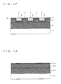
- FIGS. 13 to 17 are cross sections showing a method of forming a buried copper wiring in the background art step by step.
- an underlying insulating film 102 made of silicon oxide film is formed on a silicon substrate 101 .
- semiconductor elements such as transistors are formed in the silicon substrate 101 and the underlying insulating film 102 .
- source/drain regions are selectively formed in an upper surface of the silicon substrate 101 and a gate electrode is selectively formed on the upper surface of the silicon substrate 101 .
- source/drain wirings connected to the source/drain regions are selectively formed in the underlying insulating film 102 .
- the first interlayer insulating film 103 is an insulating film made of a material having lower relative dielectric constant than that of the silicon oxide film.
- a film such as Hydrogen Silsesquioxane, Methyl Silsesquioxane (MSQ), Poly arylether, Benzocyclobutene, Polytetrafluoroethylene, Xerogel or Aerogel is formed by the spin-on method.
- a film such as SiOF film, CF film, Parylene or SiOC film is formed by the CVD (Chemical Vapor Deposition) method.
- the relative dielectric constants of these materials range from about 1.8 to 3.7.
- a second interlayer insulating film 104 is formed on the first interlayer insulating film 103 .
- a silicon nitride film (whose relative dielectric constant is 7.4), a silicon oxide film (whose relative dielectric constant ranges from 4.3 to 4.5), a silicon carbide film (whose relative dielectric constant ranges from 4.3 to 4.7) or the like is used.
- a photoresist 105 having a pattern with openings above regions in which the copper wirings are to be formed is formed on the second interlayer insulating film 104 by photolithography.
- the second interlayer insulating film 104 and the first interlayer insulating film 103 are etched in this order by anisotropic dry etching with high etching rate in a direction of depth of the silicon substrate 101 , to expose an upper surface of the underlying insulating film 102 .
- a recess 106 having a bottom surface defined by the upper surface of the underlying insulating film 102 and a side surface defined by a sidewall of the first interlayer insulating film 103 and a sidewall of the second interlayer insulating film 104 .
- the photoresist 105 is removed by ashing process using oxygen gas plasma 107 .
- the ashing process is performed under a plasma forming condition that the RF power is 900 W, the chamber pressure is 133 Pa, the oxygen flow is 2000 sccm and the substrate temperature is 200° C.
- a tantalum nitride (TaN) film (not shown) is entirely formed by sputtering method and then a copper film is so formed as to have such a film thickness as to fill the inside of the recess 106 by sputtering method or plating method.
- the copper film and the TaN film are polished by the CMP (Chemical Mechanical Polishing) method until an upper surface of the second interlayer insulating film 104 is exposed.
- the TaN film is formed in order to prevent diffusion of copper atoms of the copper wiring 109 into the first and second interlayer insulating films 103 and 104 .
- the ashing process using the oxygen gas plasma 107 is performed under the plasma forming condition that the chamber pressure is 133 Pa and the substrate temperature is 200° C. in the step of removing the photoresist 105 (FIG. 16).
- an insulating film including Si—C n H 2n+1 bond (n: natural number) therein such as an MSQ film or an SiOC film including Si—CH 3 bond
- the Si—CH 3 bond in the film is decomposed by the oxygen gas plasma 107 into Si—OH bond, as shown in the chemical equation (1):
- FIG. 18 is a graph showing an infrared absorption spectrum of an MSQ film with respect to the sidewall portion of the first interlayer insulating film 103 in a case where the MSQ film is adopted as the first interlayer insulating film 103 . It can be seen from FIG. 18 that a spectrum caused by Si—OH bond, which does not exist before performing the ashing process (before irradiation of gas plasma), is generated after performing the ashing process (after irradiation of gas plasma).
- the Si—OH bond has an orientational polarization component, the relative dielectric constant of the first interlayer insulating film 103 in which the damage layer 110 exists is higher than that of the first interlayer insulating film 103 in which no damage layer 110 exists. Further, since the Si—OH bond becomes an adsorption site of moisture in the atmosphere, a lot of absorbed moisture exists in the damage layer 110 and therefore the relative dielectric constant of the first interlayer insulating film 103 becomes still higher.
- FIG. 19 is a graph showing variation in relative dielectric constant of the first interlayer insulating film 103 between before and after performing the ashing process for removing the photoresist 105 .
- the relative dielectric constant after performing the ashing process (after irradiation of gas plasma) is higher than that before performing the ashing process (before irradiation of gas plasma) by 48%.
- the background-art method of forming a buried copper wiring has the following problem: when the insulating film including Si—C n H 2n+1 bond is adopted as the first interlayer insulating film 103 , much of the Si—C n H 2n+1 bond in the film is changed into Si—OH bond through the ashing process for removing the photoresist 105 and that causes a rise in relative dielectric constant of the first interlayer insulating film 103 , leading to an increase in wiring capacitance.
- the present invention is directed to a method of forming a dielectric film.
- the method of forming a dielectric film comprises the steps of: (a) forming an insulating film including Si—C n H 2n+1 bond; (b) forming a resist selectively on a main surface of the insulating film; (c) removing the insulating film not covered with the resist to form a recess in the main surface of the insulating film; and (d) performing an ashing process using gas plasma under a condition that the Si—C n H 2n+1 , bond should not be changed to Si—OH bond to remove the resist.
- the Si—C n H 2n+1 bond is changed to Si—H bond in the ashing process under the condition in the step (d).
- the condition is that oxygen gas plasma is used, the temperature is 25° C. or lower and the chamber pressure ranges from 4 to 70 Pa.
- the condition is that oxygen gas plasma is used, the temperature is 100° C. or lower and the chamber pressure ranges from 4 to 13.3 Pa.
- the ashing process is performed by using hydrogen gas plasma or ammonia gas plasma in the step (d).
- the method of forming a dielectric film of the first aspect further comprises the step of: (e) filling the inside of the recess with a metal film, and in the method, the step (e) is executed after the step (d).
- the insulating film is formed on an underlying layer in the step (a), and the recess is so formed as not to reach the underlying layer in the step (c).
- the present invention is also directed to a dielectric film.
- the dielectric film comprises: an insulating film including Si—C n H 2n+1 bond; a recess formed selectively in a main surface of the insulating film; and a surface protective layer including Si—H bond, being formed in a surface of the insulating film in an inner wall of the recess.
- the dielectric film of the sixth aspect further comprises: a metal film for filling the inside of the recess.
- the dielectric film is formed on an underlying layer, and the recess is so formed, extending from the main surface of the insulating film, as not to reach the underlying layer.
- the Si—H bond exists in the surface protective layer. Therefore, the insulating film of the sixth aspect can suppress or avoid a rise in relative dielectric constant of the insulating film, as compared with an insulating film in which a layer including the Si—OH bond, instead of the surface protective layer including the Si—H bond, is formed in its surface.
- An object of the present invention is to provide a method of forming a dielectric film and a structure thereof, which can suppress a rise in relative dielectric constant of an interlayer insulating film, which is caused by a change of Si—C n H 2n+1 bond in the film into Si—OH bond, in a buried wiring structure in which an insulating film including Si—C n H 2n+1 bond is adopted as the interlayer insulating film.
- FIGS. 1 to 5 are cross sections showing a method of forming a buried copper wiring in accordance with a first preferred embodiment step by step;
- FIG. 6 is a graph showing an infrared absorption spectrum of an MSQ film with respect to a sidewall portion of a first interlayer insulating film
- FIG. 7 is a graph showing variation in dielectric constant of the first interlayer insulating film between before and after performing an ashing process
- FIG. 8 is a graph showing a measurement result of the amount of Si—H bond generated in the first interlayer insulating film after irradiation of oxygen gas plasma under varying chamber pressures;
- FIG. 9 is a graph showing a measurement result of the amount of Si—OH bond generated in the first interlayer insulating film after irradiation of oxygen gas plasma under varying substrate temperatures;
- FIGS. 10 and 11 are cross sections each showing a step in a method of forming a buried copper wiring in accordance with a second preferred embodiment
- FIG. 12 is a cross section showing a structure formed by a method of forming a buried copper wiring in accordance with a third preferred embodiment
- FIGS. 13 to 17 are cross sections showing a method of forming a buried copper wiring in the background art step by step
- FIG. 18 is a graph showing an infrared absorption spectrum of an MSQ film with respect to a sidewall portion of the first interlayer insulating film.
- FIG. 19 is a graph showing variation in dielectric constant of the first interlayer insulating film between before and after performing an ashing process.
- FIGS. 1 to 5 are cross sections showing a method of forming a buried copper wiring in accordance with the first preferred embodiment step by step.
- an underlying insulating film 2 made of silicon oxide film is formed on a silicon substrate 1 .
- semiconductor elements such as transistors are formed in the silicon substrate 1 and the underlying insulating film 2 .
- source/drain regions are selectively formed in an upper surface of the silicon substrate 1 and a gate electrode is selectively formed on the upper surface of the silicon substrate 1 .
- source/drain wirings connected to the source/drain regions are selectively formed in the underlying insulating film 2 .
- a first interlayer insulating film 3 functioning as a dielectric film is formed on the underlying insulating film 2 .
- the first interlayer insulating film 3 may be directly formed on the silicon substrate 1 in which the semiconductor elements are formed, instead of being formed on the underlying insulating film 2 .
- the first interlayer insulating film 3 is an insulating film made of a material having lower relative dielectric constant than that of the silicon oxide film which is a general insulating film.
- the first interlayer insulating film 3 for example, a film such as Hydrogen Silsesquioxane, Methyl Silsesquioxane (MSQ), Poly arylether, Benzocyclobutene, Polytetrafluoroethylene, Xerogel or Aerogel is formed by the spin-on method. Alternatively, a film such as SiOF film, CF film, Parylene or SiOC film is formed by the CVD method. In the first preferred embodiment, as the first interlayer insulating film 3 , an insulating film (MSQ film in this preferred embodiment) including Si—C n H 2n+1 bond therein is adopted.
- a second interlayer insulating film 4 is formed on the first interlayer insulating film 3 .
- a silicon nitride film, a silicon oxide film, a silicon carbide film or the like is used as the material of the second interlayer insulating film 4 .
- the second interlayer insulating film 4 may not be necessarily formed.
- a photoresist 5 having a pattern with openings above regions in which the copper wirings are to be formed is formed on the second interlayer insulating film 4 by photolithography.
- the photoresist 5 is formed on the first interlayer insulating film 3 .
- the second interlayer insulating film 4 and the first interlayer insulating film 3 are etched in this order by anisotropic dry etching with high etching rate in a direction of depth of the silicon substrate 1 , to expose an upper surface of the underlying insulating film 2 .
- a recess 6 having a bottom surface defined by the upper surface of the underlying insulating film 2 and an inner wall defined by a sidewall of the first interlayer insulating film 3 and a sidewall of the second interlayer insulating film 4 .
- the photoresist 5 is removed by ashing process using an oxygen gas plasma 7 .
- the ashing process is performed under a plasma forming condition that the RF power is 300 W, the chamber pressure is 30 Pa, the oxygen flow is 100 sccm and the substrate temperature is 25° C.
- a surface protective layer 8 is formed inside the sidewall of the first interlayer insulating film 3 .
- FIG. 6 is a graph showing an infrared absorption spectrum of the MSQ film with respect to the sidewall portion of the first interlayer insulating film 3 . It can be seen from FIG.
- Si—H bond has no orientational polarization component and does not become an adsorption site of moisture in the atmosphere. Therefore, even if the surface protective layer 8 including Si—H bond is formed inside the sidewall of the first interlayer insulating film 3 , Si—H bond does not cause a rise in relative dielectric constant of the first interlayer insulating film 3 .
- FIG. 7 is a graph showing variation in relative dielectric constant of the first interlayer insulating film 3 between before and after performing the ashing process for removing the photoresist 5 . It can be seen from FIG. 7 that the rise in relative dielectric constant after performing the ashing process as compared with before performing the ashing process is suppressed to 14% (48% in FIG. 19 of the background art).
- a tantalum nitride (TaN) film (not shown) is entirely formed by sputtering method and then a copper film is so formed as to have such a film thickness as to fill the inside of the recess 6 by sputtering method or plating method.
- the copper film and the TaN film are polished by the CMP method until an upper surface of the second interlayer insulating film 4 is exposed.
- the TaN film is formed in order to prevent diffusion of copper atoms of the copper wiring 9 into the first and second interlayer insulating films 3 and 4 .
- FIG. 8 is a graph showing a measurement result of the amount of Si—H bond generated in the first interlayer insulating film 3 after irradiation of the oxygen gas plasma 7 under varying chamber pressures.
- the amount of Si—H on the vertical axis is represented by an area value for absorption of the infrared absorption spectrum, which is caused by Si—H bond.
- the amount of Si—H decreases as the chamber pressure rises and when the substrate temperature is 25° C., for example, almost no Si—H bond is generated when the chamber pressure becomes over 70 Pa.
- the amount of Si—OH decreases as the chamber pressure falls and when the substrate temperature is 25° C., for example, almost no Si—OH bond is generated when the chamber pressure becomes 70 Pa or lower. Therefore, in order to generate Si—H bond, instead of Si—OH bond, in the fist interlayer insulating film 3 after irradiation of the oxygen gas plasma 7 , when the substrate temperature is 25° C., for example, it is only necessary to set the upper limit of the chamber pressure to 70 Pa. Since it becomes difficult to provide the oxygen gas plasma 7 stably when the chamber pressure becomes below 4 Pa, however, it is necessary to set the lower limit of the chamber pressure to 4 Pa.
- FIG. 9 is a graph showing a measurement result of the amount of Si—OH bond generated in the first interlayer insulating film 3 after irradiation of the oxygen gas plasma 7 under fixed chamber pressure of 106 Pa and varying substrate temperatures.
- the amount of Si—OH on the vertical axis is represented by an area value for absorption of the infrared absorption spectrum, which is caused by Si—OH bond.
- the amount of Si—OH bond decreases as the substrate temperature falls, in other words, it becomes likely to generate the Si—H bond depending on the condition of chamber pressure.
- the Si—H bond can be obtained by the ashing process for removing the photoresist 5 under the condition that the chamber pressure ranges from 4 to 70 Pa when the substrate temperature is 25° C. or lower or the chamber pressure ranges from 4 to 13.3 Pa when the substrate temperature is 100° C. or lower, and further no Si—OH bond is generated under the same condition.
- the ashing process for removing the photoresist 5 is performed by using the oxygen gas plasma under the condition that the chamber pressure ranges from 4 to 70 Pa when the substrate temperature is 25° C. or lower or the chamber pressure ranges from 4 to 13.3 Pa when the substrate temperature is 100° C. or lower.
- the surface protective layer 8 including the Si—H bond, not including the Si—OH bond is formed in the surface of the first interlayer insulating film 3 in the inner wall of the recess 6 .
- FIGS. 10 and 11 are cross sections each showing a step in a method of forming a buried copper wiring in accordance with the second preferred embodiment.
- the oxygen gas plasma is used in the ashing process for removing the photoresist 5 (FIG. 4) in the first preferred embodiment
- a mixed gas of nitrogen and hydrogen as shown in FIG. 10 or an ammonia gas as shown in FIG. 11 may be used, instead of the oxygen gas.
- Other steps in the method of forming a buried copper wiring of the second preferred embodiment are the same as those in the first preferred embodiment.
- the chemical equation in a case of using the mixed gas of nitrogen and hydrogen is as follows:
- the Si—CH 3 bond is decomposed and Si—H bond is generated both in the cases. Therefore, like in the first preferred embodiment, it is possible to form the surface protective layer 8 including the Si—H bond, not including the Si—OH bond.
- the nitrogen gas is mixed from a safety standpoint and may not be necessarily mixed from a standpoint of generation of the Si—H bond.
- the surface protective layer 8 including the Si—H bond, not including the Si—OH bond in the surface of the first interlayer insulating film 3 in the inner wall of the recess 6 by performing the ashing process using the mixed gas of nitrogen and hydrogen or the ammonia gas. Therefore, it becomes possible to avoid a rise in relative dielectric constant of the first interlayer insulating film 3 .
- the recess 6 having the bottom surface defined by the upper surface of the underlying insulating film 2 is formed in the etching step of FIG. 3. At that time, there may be a case where the etching is stopped before the upper surface of the underlying insulating film 2 is exposed, to form the recess 6 having the bottom surface defined by the first interlayer insulating film 3 .
- FIG. 12 is a cross section showing a structure formed by a method of forming a buried copper wiring in accordance with the third preferred embodiment.
- the surface protective layer 8 including the Si—H bond, not including the Si—OH bond in the surface of the first interlayer insulating film 3 in the inner wall (i.e., the side surface and the bottom surface) of the recess 6 .
- the inner wall i.e., the side surface and the bottom surface
Abstract
Description
- 1. Field of the Invention
- The present invention relates to a method of forming a dielectric film and a structure thereof, and more particularly to a method of forming an interlayer dielectric film in a buried wiring structure and a structure thereof.
- 2. Description of the Background Art
- Especially in a system LSI after the 0.18-micron generation, in order to achieve speed-up of devices, it is important to reduce signal delay of the devices. The signal delay of a device is a sum of signal delay in transistors and that in interconnection. As reduction in wiring pitch rapidly proceeds, the effect of the signal delay in interconnection becomes larger than that in transistors. Since the signal delay in interconnection is in proportion to the RC product (wiring resistance×wiring capacitance), in order to reduce the signal delay in interconnection, it is necessary to reduce the wiring resistance or the wiring capacitance. Therefore, an insulating film having lower relative dielectric constant than that of a silicon oxide film which is a general insulating film is used as an interlayer insulating film and a copper wiring having lower wiring resistance than that of an aluminum wiring which is a general metal wiring is used as a buried wiring, to reduce the signal delay in interconnection.
- FIGS. 13 to 17 are cross sections showing a method of forming a buried copper wiring in the background art step by step. First, referring to FIG. 13, an underlying
insulating film 102 made of silicon oxide film is formed on asilicon substrate 101. Though not shown in FIG. 13, semiconductor elements such as transistors are formed in thesilicon substrate 101 and the underlyinginsulating film 102. For example, source/drain regions are selectively formed in an upper surface of thesilicon substrate 101 and a gate electrode is selectively formed on the upper surface of thesilicon substrate 101. Further, source/drain wirings connected to the source/drain regions are selectively formed in the underlyinginsulating film 102. - Subsequently, a first
interlayer insulating film 103 is formed on the underlyinginsulating film 102. The first interlayerinsulating film 103 is an insulating film made of a material having lower relative dielectric constant than that of the silicon oxide film. For example, a film such as Hydrogen Silsesquioxane, Methyl Silsesquioxane (MSQ), Poly arylether, Benzocyclobutene, Polytetrafluoroethylene, Xerogel or Aerogel is formed by the spin-on method. Alternatively, a film such as SiOF film, CF film, Parylene or SiOC film is formed by the CVD (Chemical Vapor Deposition) method. The relative dielectric constants of these materials range from about 1.8 to 3.7. - Subsequently, a second
interlayer insulating film 104 is formed on the first interlayerinsulating film 103. As the material of the second interlayerinsulating film 104, a silicon nitride film (whose relative dielectric constant is 7.4), a silicon oxide film (whose relative dielectric constant ranges from 4.3 to 4.5), a silicon carbide film (whose relative dielectric constant ranges from 4.3 to 4.7) or the like is used. - Next, referring to FIG. 14, a
photoresist 105 having a pattern with openings above regions in which the copper wirings are to be formed is formed on the secondinterlayer insulating film 104 by photolithography. - Next, referring to FIG. 15, using the
photoresist 105 as an etching mask, the secondinterlayer insulating film 104 and the firstinterlayer insulating film 103 are etched in this order by anisotropic dry etching with high etching rate in a direction of depth of thesilicon substrate 101, to expose an upper surface of the underlyinginsulating film 102. Through this step formed is arecess 106 having a bottom surface defined by the upper surface of the underlyinginsulating film 102 and a side surface defined by a sidewall of the firstinterlayer insulating film 103 and a sidewall of the second interlayerinsulating film 104. - Next, referring to FIG. 16, the
photoresist 105 is removed by ashing process usingoxygen gas plasma 107. The ashing process is performed under a plasma forming condition that the RF power is 900 W, the chamber pressure is 133 Pa, the oxygen flow is 2000 sccm and the substrate temperature is 200° C. - Subsequently, a tantalum nitride (TaN) film (not shown) is entirely formed by sputtering method and then a copper film is so formed as to have such a film thickness as to fill the inside of the
recess 106 by sputtering method or plating method. Next, referring to FIG. 17, the copper film and the TaN film are polished by the CMP (Chemical Mechanical Polishing) method until an upper surface of the secondinterlayer insulating film 104 is exposed. Through this step formed is acopper wiring 109 for filling the inside of therecess 106 with the not-shown TaN film interposed therebetween. Further, the TaN film is formed in order to prevent diffusion of copper atoms of thecopper wiring 109 into the first and second interlayerinsulating films - Thus, in the background-art method of forming a buried copper wiring, the ashing process using the
oxygen gas plasma 107 is performed under the plasma forming condition that the chamber pressure is 133 Pa and the substrate temperature is 200° C. in the step of removing the photoresist 105 (FIG. 16). For this reason, when an insulating film including Si—CnH2n+1 bond (n: natural number) therein, such as an MSQ film or an SiOC film including Si—CH3 bond, is used as the first interlayerinsulating film 103, the Si—CH3 bond in the film is decomposed by theoxygen gas plasma 107 into Si—OH bond, as shown in the chemical equation (1): - Si−CH3+2O2→Si−OH+CO2+H2O (1)
- As a result, as shown in FIG. 16, a
damage layer 110 including a lot of Si—OH bond is formed inside the inner wall of the firstinterlayer insulating film 103. FIG. 18 is a graph showing an infrared absorption spectrum of an MSQ film with respect to the sidewall portion of the firstinterlayer insulating film 103 in a case where the MSQ film is adopted as the first interlayerinsulating film 103. It can be seen from FIG. 18 that a spectrum caused by Si—OH bond, which does not exist before performing the ashing process (before irradiation of gas plasma), is generated after performing the ashing process (after irradiation of gas plasma). - Since the Si—OH bond has an orientational polarization component, the relative dielectric constant of the first interlayer
insulating film 103 in which thedamage layer 110 exists is higher than that of the first interlayerinsulating film 103 in which nodamage layer 110 exists. Further, since the Si—OH bond becomes an adsorption site of moisture in the atmosphere, a lot of absorbed moisture exists in thedamage layer 110 and therefore the relative dielectric constant of the firstinterlayer insulating film 103 becomes still higher. - FIG. 19 is a graph showing variation in relative dielectric constant of the first
interlayer insulating film 103 between before and after performing the ashing process for removing thephotoresist 105. The relative dielectric constant after performing the ashing process (after irradiation of gas plasma) is higher than that before performing the ashing process (before irradiation of gas plasma) by 48%. - Thus, the background-art method of forming a buried copper wiring has the following problem: when the insulating film including Si—C nH2n+1 bond is adopted as the first
interlayer insulating film 103, much of the Si—CnH2n+1 bond in the film is changed into Si—OH bond through the ashing process for removing thephotoresist 105 and that causes a rise in relative dielectric constant of the first interlayerinsulating film 103, leading to an increase in wiring capacitance. - The present invention is directed to a method of forming a dielectric film. According to a first aspect of the present invention, the method of forming a dielectric film comprises the steps of: (a) forming an insulating film including Si—C nH2n+1 bond; (b) forming a resist selectively on a main surface of the insulating film; (c) removing the insulating film not covered with the resist to form a recess in the main surface of the insulating film; and (d) performing an ashing process using gas plasma under a condition that the Si—CnH2n+1, bond should not be changed to Si—OH bond to remove the resist.
- According to a second aspect of the present invention, in the method of forming a dielectric film of the first aspect, the Si—C nH2n+1 bond is changed to Si—H bond in the ashing process under the condition in the step (d).
- According to a third aspect of the present invention, in the method of forming a dielectric film of the first aspect, the condition is that oxygen gas plasma is used, the temperature is 25° C. or lower and the chamber pressure ranges from 4 to 70 Pa.
- According to a fourth aspect of the present invention, in the method of forming a dielectric film of the first aspect, the condition is that oxygen gas plasma is used, the temperature is 100° C. or lower and the chamber pressure ranges from 4 to 13.3 Pa.
- According to a fifth aspect of the present invention, in the method of forming a dielectric film of the first aspect, the ashing process is performed by using hydrogen gas plasma or ammonia gas plasma in the step (d).
- Preferably, the method of forming a dielectric film of the first aspect further comprises the step of: (e) filling the inside of the recess with a metal film, and in the method, the step (e) is executed after the step (d).
- Preferably, the insulating film is formed on an underlying layer in the step (a), and the recess is so formed as not to reach the underlying layer in the step (c).
- The present invention is also directed to a dielectric film. According to a sixth aspect of the present invention, the dielectric film comprises: an insulating film including Si—C nH2n+1 bond; a recess formed selectively in a main surface of the insulating film; and a surface protective layer including Si—H bond, being formed in a surface of the insulating film in an inner wall of the recess.
- Preferably, the dielectric film of the sixth aspect further comprises: a metal film for filling the inside of the recess.
- Preferably, the dielectric film is formed on an underlying layer, and the recess is so formed, extending from the main surface of the insulating film, as not to reach the underlying layer.
- In the method of forming an insulating film of the first and second aspects, since the Si—C nH2n+1 bond included in the surface of the insulating film in the inner wall of the recess is not changed to the Si—OH bond through the ashing process in the step (d), it is possible to suppress a rise in relative dielectric constant of the insulating film.
- In the method of forming an insulating film of the third and fourth aspects, it is possible to appropriately change the Si—C nH2n+1 bond included in the insulating film to the Si—H bond.
- In the method of forming an insulating film of the fifth aspect, it is possible to avoid the change of the Si—C nH2+1 bond included in the insulating film into the Si—OH bond and suppress a rise in relative dielectric constant of the insulating film, which is caused by the Si—OH bond.
- In the insulating film of the sixth aspect, the Si—H bond exists in the surface protective layer. Therefore, the insulating film of the sixth aspect can suppress or avoid a rise in relative dielectric constant of the insulating film, as compared with an insulating film in which a layer including the Si—OH bond, instead of the surface protective layer including the Si—H bond, is formed in its surface.
- An object of the present invention is to provide a method of forming a dielectric film and a structure thereof, which can suppress a rise in relative dielectric constant of an interlayer insulating film, which is caused by a change of Si—C nH2n+1 bond in the film into Si—OH bond, in a buried wiring structure in which an insulating film including Si—CnH2n+1 bond is adopted as the interlayer insulating film.
- These and other objects, features, aspects and advantages of the present invention will become more apparent from the following detailed description of the present invention when taken in conjunction with the accompanying drawings.
- FIGS. 1 to 5 are cross sections showing a method of forming a buried copper wiring in accordance with a first preferred embodiment step by step;
- FIG. 6 is a graph showing an infrared absorption spectrum of an MSQ film with respect to a sidewall portion of a first interlayer insulating film;
- FIG. 7 is a graph showing variation in dielectric constant of the first interlayer insulating film between before and after performing an ashing process;
- FIG. 8 is a graph showing a measurement result of the amount of Si—H bond generated in the first interlayer insulating film after irradiation of oxygen gas plasma under varying chamber pressures;
- FIG. 9 is a graph showing a measurement result of the amount of Si—OH bond generated in the first interlayer insulating film after irradiation of oxygen gas plasma under varying substrate temperatures;
- FIGS. 10 and 11 are cross sections each showing a step in a method of forming a buried copper wiring in accordance with a second preferred embodiment;
- FIG. 12 is a cross section showing a structure formed by a method of forming a buried copper wiring in accordance with a third preferred embodiment;
- FIGS. 13 to 17 are cross sections showing a method of forming a buried copper wiring in the background art step by step;
- FIG. 18 is a graph showing an infrared absorption spectrum of an MSQ film with respect to a sidewall portion of the first interlayer insulating film; and
- FIG. 19 is a graph showing variation in dielectric constant of the first interlayer insulating film between before and after performing an ashing process.
- FIGS. 1 to 5 are cross sections showing a method of forming a buried copper wiring in accordance with the first preferred embodiment step by step. First, referring to FIG. 1, an underlying
insulating film 2 made of silicon oxide film is formed on asilicon substrate 1. Though not shown in FIG. 1, semiconductor elements such as transistors are formed in thesilicon substrate 1 and the underlying insulatingfilm 2. For example, source/drain regions are selectively formed in an upper surface of thesilicon substrate 1 and a gate electrode is selectively formed on the upper surface of thesilicon substrate 1. Further, source/drain wirings connected to the source/drain regions are selectively formed in the underlying insulatingfilm 2. - Subsequently, a first
interlayer insulating film 3 functioning as a dielectric film is formed on the underlying insulatingfilm 2. The firstinterlayer insulating film 3, however, may be directly formed on thesilicon substrate 1 in which the semiconductor elements are formed, instead of being formed on the underlying insulatingfilm 2. The firstinterlayer insulating film 3 is an insulating film made of a material having lower relative dielectric constant than that of the silicon oxide film which is a general insulating film. As the firstinterlayer insulating film 3, for example, a film such as Hydrogen Silsesquioxane, Methyl Silsesquioxane (MSQ), Poly arylether, Benzocyclobutene, Polytetrafluoroethylene, Xerogel or Aerogel is formed by the spin-on method. Alternatively, a film such as SiOF film, CF film, Parylene or SiOC film is formed by the CVD method. In the first preferred embodiment, as the firstinterlayer insulating film 3, an insulating film (MSQ film in this preferred embodiment) including Si—CnH2n+1 bond therein is adopted. - Subsequently, a second
interlayer insulating film 4 is formed on the firstinterlayer insulating film 3. As the material of the secondinterlayer insulating film 4, a silicon nitride film, a silicon oxide film, a silicon carbide film or the like is used. The secondinterlayer insulating film 4, however, may not be necessarily formed. - Next, referring to FIG. 2, a
photoresist 5 having a pattern with openings above regions in which the copper wirings are to be formed is formed on the secondinterlayer insulating film 4 by photolithography. When the secondinterlayer insulating film 4 is not formed, thephotoresist 5 is formed on the firstinterlayer insulating film 3. - Next, referring to FIG. 3, using the
photoresist 5 as an etching mask, the secondinterlayer insulating film 4 and the firstinterlayer insulating film 3 are etched in this order by anisotropic dry etching with high etching rate in a direction of depth of thesilicon substrate 1, to expose an upper surface of the underlying insulatingfilm 2. Through this step formed is arecess 6 having a bottom surface defined by the upper surface of the underlying insulatingfilm 2 and an inner wall defined by a sidewall of the firstinterlayer insulating film 3 and a sidewall of the secondinterlayer insulating film 4. - Next, referring to FIG. 4, the
photoresist 5 is removed by ashing process using an oxygen gas plasma 7. The ashing process is performed under a plasma forming condition that the RF power is 300 W, the chamber pressure is 30 Pa, the oxygen flow is 100 sccm and the substrate temperature is 25° C. When the ashing process is performed under such a condition as above, as shown in FIG. 4, a surfaceprotective layer 8 is formed inside the sidewall of the firstinterlayer insulating film 3. FIG. 6 is a graph showing an infrared absorption spectrum of the MSQ film with respect to the sidewall portion of the firstinterlayer insulating film 3. It can be seen from FIG. 6 that a spectrum caused by Si—H bond, which does not exist before performing the ashing process (before irradiation of the oxygen gas plasma 7 on the first interlayer insulating film 3), is generated after performing the ashing process (after irradiation of the oxygen gas plasma 7 on the first interlayer insulating film 3). The reason is that Si—CH3 bond in the MSQ film is decomposed by the oxygen gas plasma 7 into Si—H bond, as shown in the chemical equation (2): - Si−CH3+O2→Si−H+CO+H2O (2)
- Unlike Si—OH bond, Si—H bond has no orientational polarization component and does not become an adsorption site of moisture in the atmosphere. Therefore, even if the surface
protective layer 8 including Si—H bond is formed inside the sidewall of the firstinterlayer insulating film 3, Si—H bond does not cause a rise in relative dielectric constant of the firstinterlayer insulating film 3. - FIG. 7 is a graph showing variation in relative dielectric constant of the first
interlayer insulating film 3 between before and after performing the ashing process for removing thephotoresist 5. It can be seen from FIG. 7 that the rise in relative dielectric constant after performing the ashing process as compared with before performing the ashing process is suppressed to 14% (48% in FIG. 19 of the background art). - Subsequently, a tantalum nitride (TaN) film (not shown) is entirely formed by sputtering method and then a copper film is so formed as to have such a film thickness as to fill the inside of the
recess 6 by sputtering method or plating method. Next, referring to FIG. 5, the copper film and the TaN film are polished by the CMP method until an upper surface of the secondinterlayer insulating film 4 is exposed. Through this step formed is acopper wiring 9 for filling the inside of therecess 6 with the not-shown TaN film interposed therebetween. Further, the TaN film is formed in order to prevent diffusion of copper atoms of thecopper wiring 9 into the first and secondinterlayer insulating films - The condition to obtain Si—H bond, instead of Si—OH bond, by the ashing process for removing the
photoresist 5 is as follows. - FIG. 8 is a graph showing a measurement result of the amount of Si—H bond generated in the first
interlayer insulating film 3 after irradiation of the oxygen gas plasma 7 under varying chamber pressures. In FIG. 8, the amount of Si—H on the vertical axis is represented by an area value for absorption of the infrared absorption spectrum, which is caused by Si—H bond. As can be seen from FIG. 8, the amount of Si—H decreases as the chamber pressure rises and when the substrate temperature is 25° C., for example, almost no Si—H bond is generated when the chamber pressure becomes over 70 Pa. Further, the amount of Si—OH decreases as the chamber pressure falls and when the substrate temperature is 25° C., for example, almost no Si—OH bond is generated when the chamber pressure becomes 70 Pa or lower. Therefore, in order to generate Si—H bond, instead of Si—OH bond, in the fistinterlayer insulating film 3 after irradiation of the oxygen gas plasma 7, when the substrate temperature is 25° C., for example, it is only necessary to set the upper limit of the chamber pressure to 70 Pa. Since it becomes difficult to provide the oxygen gas plasma 7 stably when the chamber pressure becomes below 4 Pa, however, it is necessary to set the lower limit of the chamber pressure to 4 Pa. - Further, as shown in FIG. 8, when the substrate temperature is 100° C., no Si—OH bond is detected and Si—H bond is generated in the
interlayer insulating film 3 both in the cases where the chamber pressure is 4 Pa and 13.3 Pa. Therefore, when the substrate temperature is 100° C., the effect of the present invention can be produced at least in the range of the chamber pressure from 4 to 13.3 Pa. - FIG. 9 is a graph showing a measurement result of the amount of Si—OH bond generated in the first
interlayer insulating film 3 after irradiation of the oxygen gas plasma 7 under fixed chamber pressure of 106 Pa and varying substrate temperatures. In FIG. 9, the amount of Si—OH on the vertical axis is represented by an area value for absorption of the infrared absorption spectrum, which is caused by Si—OH bond. As can be seen from FIG. 9, the amount of Si—OH bond decreases as the substrate temperature falls, in other words, it becomes likely to generate the Si—H bond depending on the condition of chamber pressure. - Therefore, it can be seen from FIGS. 8 and 9 that the Si—H bond can be obtained by the ashing process for removing the
photoresist 5 under the condition that the chamber pressure ranges from 4 to 70 Pa when the substrate temperature is 25° C. or lower or the chamber pressure ranges from 4 to 13.3 Pa when the substrate temperature is 100° C. or lower, and further no Si—OH bond is generated under the same condition. - In the method of forming a buried copper wiring of the first preferred embodiment, the ashing process for removing the
photoresist 5 is performed by using the oxygen gas plasma under the condition that the chamber pressure ranges from 4 to 70 Pa when the substrate temperature is 25° C. or lower or the chamber pressure ranges from 4 to 13.3 Pa when the substrate temperature is 100° C. or lower. Through this ashing process formed is the surfaceprotective layer 8 including the Si—H bond, not including the Si—OH bond, in the surface of the firstinterlayer insulating film 3 in the inner wall of therecess 6. As a result, it becomes possible to suppress a rise in relative dielectric constant of the firstinterlayer insulating film 3. - FIGS. 10 and 11 are cross sections each showing a step in a method of forming a buried copper wiring in accordance with the second preferred embodiment. Though the oxygen gas plasma is used in the ashing process for removing the photoresist 5 (FIG. 4) in the first preferred embodiment, a mixed gas of nitrogen and hydrogen as shown in FIG. 10 or an ammonia gas as shown in FIG. 11 may be used, instead of the oxygen gas. Other steps in the method of forming a buried copper wiring of the second preferred embodiment are the same as those in the first preferred embodiment. The chemical equation in a case of using the mixed gas of nitrogen and hydrogen is as follows:
- Si−CH3+H2+N2→Si−H+CH4+N2 (3)
- The chemical equation in a case of using the ammonia gas is as follows:
- Si−CH3+NH3→Si−H+CH4+N+H (4)
- It can be seen from the equations (3) and (4) that the Si—CH 3 bond is decomposed and Si—H bond is generated both in the cases. Therefore, like in the first preferred embodiment, it is possible to form the surface
protective layer 8 including the Si—H bond, not including the Si—OH bond. In the case of using the mixed gas of nitrogen and hydrogen, the nitrogen gas is mixed from a safety standpoint and may not be necessarily mixed from a standpoint of generation of the Si—H bond. - Thus, in the method of forming a buried copper wiring of the second preferred embodiment, it is possible to form the surface
protective layer 8 including the Si—H bond, not including the Si—OH bond, in the surface of the firstinterlayer insulating film 3 in the inner wall of therecess 6 by performing the ashing process using the mixed gas of nitrogen and hydrogen or the ammonia gas. Therefore, it becomes possible to avoid a rise in relative dielectric constant of the firstinterlayer insulating film 3. - In the above method of forming a buried copper wiring of the first and second preferred embodiments, the
recess 6 having the bottom surface defined by the upper surface of the underlying insulatingfilm 2 is formed in the etching step of FIG. 3. At that time, there may be a case where the etching is stopped before the upper surface of the underlying insulatingfilm 2 is exposed, to form therecess 6 having the bottom surface defined by the firstinterlayer insulating film 3. - Next, the
photoresist 5 is removed by the ashing process using the oxygen gas plasma (in the first preferred embodiment) or the ashing process using the mixed gas of nitrogen and hydrogen or the ammonia gas (in the second preferred embodiment). The ashing process is performed under the same condition as in the first and second preferred embodiments. After that, like in the first and second preferred embodiments, the TaN film is formed and then thecopper wiring 9 is formed to fill the inside of therecess 6 with the TaN film interposed therebetween. FIG. 12 is a cross section showing a structure formed by a method of forming a buried copper wiring in accordance with the third preferred embodiment. - Thus, in the method of forming a buried copper wiring of the third preferred embodiment, it is possible to form the surface
protective layer 8 including the Si—H bond, not including the Si—OH bond, in the surface of the firstinterlayer insulating film 3 in the inner wall (i.e., the side surface and the bottom surface) of therecess 6. As a result, it becomes possible to avoid a rise in relative dielectric constant of the firstinterlayer insulating film 3. - While the invention has been shown and described in detail, the foregoing description is in all aspects illustrative and not restrictive. It is therefore understood that numerous modifications and variations can be devised without departing from the scope of the invention.
Claims (10)
Priority Applications (1)
| Application Number | Priority Date | Filing Date | Title |
|---|---|---|---|
| US10/196,181 US6903027B2 (en) | 2001-01-05 | 2002-07-17 | Method of forming dielectric film and dielectric film |
Applications Claiming Priority (2)
| Application Number | Priority Date | Filing Date | Title |
|---|---|---|---|
| JP2001000627A JP2002203852A (en) | 2001-01-05 | 2001-01-05 | Forming method of insulation film and the insulation film |
| JP2001-000627 | 2001-01-05 |
Related Child Applications (1)
| Application Number | Title | Priority Date | Filing Date |
|---|---|---|---|
| US10/196,181 Division US6903027B2 (en) | 2001-01-05 | 2002-07-17 | Method of forming dielectric film and dielectric film |
Publications (1)
| Publication Number | Publication Date |
|---|---|
| US20020090833A1 true US20020090833A1 (en) | 2002-07-11 |
Family
ID=18869380
Family Applications (2)
| Application Number | Title | Priority Date | Filing Date |
|---|---|---|---|
| US09/963,648 Abandoned US20020090833A1 (en) | 2001-01-05 | 2001-09-27 | Method of forming dielectric film and dielectric film |
| US10/196,181 Expired - Lifetime US6903027B2 (en) | 2001-01-05 | 2002-07-17 | Method of forming dielectric film and dielectric film |
Family Applications After (1)
| Application Number | Title | Priority Date | Filing Date |
|---|---|---|---|
| US10/196,181 Expired - Lifetime US6903027B2 (en) | 2001-01-05 | 2002-07-17 | Method of forming dielectric film and dielectric film |
Country Status (2)
| Country | Link |
|---|---|
| US (2) | US20020090833A1 (en) |
| JP (1) | JP2002203852A (en) |
Cited By (8)
| Publication number | Priority date | Publication date | Assignee | Title |
|---|---|---|---|---|
| WO2004038788A2 (en) * | 2002-10-24 | 2004-05-06 | Lam Research Corporation | Method and apparatus for detecting endpoint during plasma etching of thin films |
| US20040235293A1 (en) * | 2003-05-21 | 2004-11-25 | Semiconductor Leading Edge Technologies, Inc. | Method for manufacturing semiconductor device |
| US20090078675A1 (en) * | 2007-09-26 | 2009-03-26 | Silverbrook Research Pty Ltd | Method of removing photoresist |
| WO2009039551A1 (en) * | 2007-09-26 | 2009-04-02 | Silverbrook Research Pty Ltd | Method of removing photoresist |
| CN102509699A (en) * | 2011-11-02 | 2012-06-20 | 上海宏力半导体制造有限公司 | Metal layer photoresist repainting method and photoetching method |
| US20140247557A1 (en) * | 2013-03-04 | 2014-09-04 | The Hong Kong University Of Science And Technology | Phase-change chamber with patterned regions of high and low affinity to a phase-change medium for electronic device cooling |
| US10381322B1 (en) | 2018-04-23 | 2019-08-13 | Sandisk Technologies Llc | Three-dimensional memory device containing self-aligned interlocking bonded structure and method of making the same |
| US10879260B2 (en) | 2019-02-28 | 2020-12-29 | Sandisk Technologies Llc | Bonded assembly of a support die and plural memory dies containing laterally shifted vertical interconnections and methods for making the same |
Families Citing this family (9)
| Publication number | Priority date | Publication date | Assignee | Title |
|---|---|---|---|---|
| US6759098B2 (en) * | 2000-03-20 | 2004-07-06 | Axcelis Technologies, Inc. | Plasma curing of MSQ-based porous low-k film materials |
| JP2002324837A (en) * | 2001-04-25 | 2002-11-08 | Hitachi Ltd | Manufacturing method of semiconductor device |
| US20030155657A1 (en) | 2002-02-14 | 2003-08-21 | Nec Electronics Corporation | Manufacturing method of semiconductor device |
| KR100439844B1 (en) * | 2002-07-24 | 2004-07-12 | 삼성전자주식회사 | method for removing photoresist after metal layer etching in semiconductor device |
| US7288488B2 (en) * | 2005-05-10 | 2007-10-30 | Lam Research Corporation | Method for resist strip in presence of regular low k and/or porous low k dielectric materials |
| US7416990B2 (en) * | 2005-12-20 | 2008-08-26 | Dongbu Electronics Co., Ltd. | Method for patterning low dielectric layer of semiconductor device |
| US7553736B2 (en) * | 2006-07-13 | 2009-06-30 | Taiwan Semiconductor Manufacturing Company, Ltd. | Increasing dielectric constant in local regions for the formation of capacitors |
| JP5067068B2 (en) | 2007-08-17 | 2012-11-07 | 東京エレクトロン株式会社 | Semiconductor device manufacturing method and storage medium |
| US8871639B2 (en) | 2013-01-04 | 2014-10-28 | Taiwan Semiconductor Manufacturing Company, Ltd. | Semiconductor devices and methods of manufacture thereof |
Family Cites Families (10)
| Publication number | Priority date | Publication date | Assignee | Title |
|---|---|---|---|---|
| US5177588A (en) | 1991-06-14 | 1993-01-05 | Mitsubishi Denki Kabushiki Kaisha | Semiconductor device including nitride layer |
| JP3204041B2 (en) | 1995-05-19 | 2001-09-04 | ソニー株式会社 | Method of forming insulating film |
| JPH0992717A (en) | 1995-09-21 | 1997-04-04 | Mitsubishi Electric Corp | Semiconductor and fabrication thereof |
| JPH11150101A (en) * | 1997-11-18 | 1999-06-02 | Nec Corp | Manufacture of semiconductor device |
| JP3193335B2 (en) | 1997-12-12 | 2001-07-30 | 松下電器産業株式会社 | Method for manufacturing semiconductor device |
| JP3248492B2 (en) | 1998-08-14 | 2002-01-21 | 日本電気株式会社 | Semiconductor device and manufacturing method thereof |
| JP2000077410A (en) | 1998-08-27 | 2000-03-14 | Tokyo Ohka Kogyo Co Ltd | Forming method of multilayer interconnection structure |
| US6207583B1 (en) * | 1998-09-04 | 2001-03-27 | Alliedsignal Inc. | Photoresist ashing process for organic and inorganic polymer dielectric materials |
| US6117782A (en) * | 1999-04-22 | 2000-09-12 | Advanced Micro Devices, Inc. | Optimized trench/via profile for damascene filling |
| US6457477B1 (en) * | 2000-07-24 | 2002-10-01 | Taiwan Semiconductor Manufacturing Company | Method of cleaning a copper/porous low-k dual damascene etch |
-
2001
- 2001-01-05 JP JP2001000627A patent/JP2002203852A/en active Pending
- 2001-09-27 US US09/963,648 patent/US20020090833A1/en not_active Abandoned
-
2002
- 2002-07-17 US US10/196,181 patent/US6903027B2/en not_active Expired - Lifetime
Cited By (12)
| Publication number | Priority date | Publication date | Assignee | Title |
|---|---|---|---|---|
| WO2004038788A2 (en) * | 2002-10-24 | 2004-05-06 | Lam Research Corporation | Method and apparatus for detecting endpoint during plasma etching of thin films |
| WO2004038788A3 (en) * | 2002-10-24 | 2004-08-19 | Lam Res Corp | Method and apparatus for detecting endpoint during plasma etching of thin films |
| US6908846B2 (en) | 2002-10-24 | 2005-06-21 | Lam Research Corporation | Method and apparatus for detecting endpoint during plasma etching of thin films |
| US20040235293A1 (en) * | 2003-05-21 | 2004-11-25 | Semiconductor Leading Edge Technologies, Inc. | Method for manufacturing semiconductor device |
| US7172965B2 (en) | 2003-05-21 | 2007-02-06 | Rohm Co., Ltd. | Method for manufacturing semiconductor device |
| US20090078675A1 (en) * | 2007-09-26 | 2009-03-26 | Silverbrook Research Pty Ltd | Method of removing photoresist |
| WO2009039551A1 (en) * | 2007-09-26 | 2009-04-02 | Silverbrook Research Pty Ltd | Method of removing photoresist |
| CN102509699A (en) * | 2011-11-02 | 2012-06-20 | 上海宏力半导体制造有限公司 | Metal layer photoresist repainting method and photoetching method |
| US20140247557A1 (en) * | 2013-03-04 | 2014-09-04 | The Hong Kong University Of Science And Technology | Phase-change chamber with patterned regions of high and low affinity to a phase-change medium for electronic device cooling |
| US9685393B2 (en) * | 2013-03-04 | 2017-06-20 | The Hong Kong University Of Science And Technology | Phase-change chamber with patterned regions of high and low affinity to a phase-change medium for electronic device cooling |
| US10381322B1 (en) | 2018-04-23 | 2019-08-13 | Sandisk Technologies Llc | Three-dimensional memory device containing self-aligned interlocking bonded structure and method of making the same |
| US10879260B2 (en) | 2019-02-28 | 2020-12-29 | Sandisk Technologies Llc | Bonded assembly of a support die and plural memory dies containing laterally shifted vertical interconnections and methods for making the same |
Also Published As
| Publication number | Publication date |
|---|---|
| US6903027B2 (en) | 2005-06-07 |
| JP2002203852A (en) | 2002-07-19 |
| US20020182891A1 (en) | 2002-12-05 |
Similar Documents
| Publication | Publication Date | Title |
|---|---|---|
| US6903027B2 (en) | Method of forming dielectric film and dielectric film | |
| US6838300B2 (en) | Chemical treatment of low-k dielectric films | |
| US6617244B2 (en) | Etching method | |
| US7741224B2 (en) | Plasma treatment and repair processes for reducing sidewall damage in low-k dielectrics | |
| US20040152296A1 (en) | Hexamethyldisilazane treatment of low-k dielectric films | |
| US6479407B2 (en) | Semiconductor device and process for producing the same | |
| US6972253B2 (en) | Method for forming dielectric barrier layer in damascene structure | |
| US6479380B2 (en) | Semiconductor device and manufacturing method thereof | |
| US6599839B1 (en) | Plasma etch process for nonhomogenous film | |
| US7015133B2 (en) | Dual damascene structure formed of low-k dielectric materials | |
| JP2001077196A (en) | Manufacture of semiconductor device | |
| US10453700B2 (en) | Low damage low-k dielectric etch | |
| US7253524B2 (en) | Copper interconnects | |
| US6528886B2 (en) | Intermetal dielectric layer for integrated circuits | |
| JP2009147096A (en) | Semiconductor device and method of manufacturing same | |
| US6774031B2 (en) | Method of forming dual-damascene structure | |
| US10177091B2 (en) | Interconnect structure and method of forming | |
| JP2006128542A (en) | Method for manufacturing electronic device | |
| US7170177B2 (en) | Semiconductor apparatus | |
| US20120199980A1 (en) | Integrated circuits having interconnect structures and methods for fabricating integrated circuits having interconnect structures | |
| US6492276B1 (en) | Hard masking method for forming residue free oxygen containing plasma etched layer | |
| JP2011082308A (en) | Method of manufacturing semiconductor apparatus | |
| US6548400B2 (en) | Method of fabricating interlevel connectors using only one photomask step | |
| US20100301494A1 (en) | Re-establishing a hydrophobic surface of sensitive low-k dielectrics in microstructure devices | |
| US6417118B1 (en) | Method for improving the moisture absorption of porous low dielectric film |
Legal Events
| Date | Code | Title | Description |
|---|---|---|---|
| AS | Assignment |
Owner name: MITSUBISHI DENKI KABUSHIKI KAISHA, JAPAN Free format text: ASSIGNMENT OF ASSIGNORS INTEREST;ASSIGNOR:MATSUURA, MASAZUMI;REEL/FRAME:012299/0005 Effective date: 20010905 |
|
| AS | Assignment |
Owner name: MITSUBISHI DENKI KABUSHIKI KAISHA, JAPAN Free format text: CORRECTED RECORDATION FORM COVER SHEET TO CORRECT ASSIGNOR'S DOC. DATE, PREVIOUSLY RECORDED AT REEL/FRAME 012299/0005 (ASSIGNMENT OF ASSIGNOR'S INTEREST);ASSIGNOR:MATSUURA, MASAZUMI;REEL/FRAME:012602/0609 Effective date: 20011031 |
|
| STCB | Information on status: application discontinuation |
Free format text: ABANDONED -- FAILURE TO RESPOND TO AN OFFICE ACTION |