US1858037A - Zero correcting circuit - Google Patents
Zero correcting circuit Download PDFInfo
- Publication number
- US1858037A US1858037A US293816A US29381628A US1858037A US 1858037 A US1858037 A US 1858037A US 293816 A US293816 A US 293816A US 29381628 A US29381628 A US 29381628A US 1858037 A US1858037 A US 1858037A
- Authority
- US
- United States
- Prior art keywords
- current
- circuit
- impulses
- zero
- windings
- Prior art date
- Legal status (The legal status is an assumption and is not a legal conclusion. Google has not performed a legal analysis and makes no representation as to the accuracy of the status listed.)
- Expired - Lifetime
Links
- 238000004804 winding Methods 0.000 description 45
- 230000011664 signaling Effects 0.000 description 28
- 239000011162 core material Substances 0.000 description 10
- 230000035699 permeability Effects 0.000 description 9
- 229920006395 saturated elastomer Polymers 0.000 description 7
- 230000008878 coupling Effects 0.000 description 6
- 238000010168 coupling process Methods 0.000 description 6
- 238000005859 coupling reaction Methods 0.000 description 6
- 230000000694 effects Effects 0.000 description 4
- 230000001939 inductive effect Effects 0.000 description 2
- 230000004048 modification Effects 0.000 description 2
- 238000012986 modification Methods 0.000 description 2
- 235000007575 Calluna vulgaris Nutrition 0.000 description 1
- 101001098066 Naja melanoleuca Basic phospholipase A2 1 Proteins 0.000 description 1
- 230000005540 biological transmission Effects 0.000 description 1
- 239000004020 conductor Substances 0.000 description 1
- QVRVXSZKCXFBTE-UHFFFAOYSA-N n-[4-(6,7-dimethoxy-3,4-dihydro-1h-isoquinolin-2-yl)butyl]-2-(2-fluoroethoxy)-5-methylbenzamide Chemical compound C1C=2C=C(OC)C(OC)=CC=2CCN1CCCCNC(=O)C1=CC(C)=CC=C1OCCF QVRVXSZKCXFBTE-UHFFFAOYSA-N 0.000 description 1
- 230000001105 regulatory effect Effects 0.000 description 1
- 238000009877 rendering Methods 0.000 description 1
- 230000000630 rising effect Effects 0.000 description 1
- 238000013022 venting Methods 0.000 description 1
Images
Classifications
-
- H—ELECTRICITY
- H04—ELECTRIC COMMUNICATION TECHNIQUE
- H04L—TRANSMISSION OF DIGITAL INFORMATION, e.g. TELEGRAPHIC COMMUNICATION
- H04L25/00—Baseband systems
- H04L25/02—Details ; arrangements for supplying electrical power along data transmission lines
- H04L25/06—DC level restoring means; Bias distortion correction ; Decision circuits providing symbol by symbol detection
- H04L25/061—DC level restoring means; Bias distortion correction ; Decision circuits providing symbol by symbol detection providing hard decisions only; arrangements for tracking or suppressing unwanted low frequency components, e.g. removal of DC offset
- H04L25/062—Setting decision thresholds using feedforward techniques only
-
- H—ELECTRICITY
- H04—ELECTRIC COMMUNICATION TECHNIQUE
- H04L—TRANSMISSION OF DIGITAL INFORMATION, e.g. TELEGRAPHIC COMMUNICATION
- H04L25/00—Baseband systems
- H04L25/02—Details ; arrangements for supplying electrical power along data transmission lines
- H04L25/03—Shaping networks in transmitter or receiver, e.g. adaptive shaping networks
- H04L25/03006—Arrangements for removing intersymbol interference
- H04L25/03012—Arrangements for removing intersymbol interference operating in the time domain
- H04L25/03114—Arrangements for removing intersymbol interference operating in the time domain non-adaptive, i.e. not adjustable, manually adjustable, or adjustable only during the reception of special signals
- H04L25/03127—Arrangements for removing intersymbol interference operating in the time domain non-adaptive, i.e. not adjustable, manually adjustable, or adjustable only during the reception of special signals using only passive components
-
- H—ELECTRICITY
- H04—ELECTRIC COMMUNICATION TECHNIQUE
- H04L—TRANSMISSION OF DIGITAL INFORMATION, e.g. TELEGRAPHIC COMMUNICATION
- H04L25/00—Baseband systems
- H04L25/02—Details ; arrangements for supplying electrical power along data transmission lines
- H04L25/06—DC level restoring means; Bias distortion correction ; Decision circuits providing symbol by symbol detection
- H04L25/061—DC level restoring means; Bias distortion correction ; Decision circuits providing symbol by symbol detection providing hard decisions only; arrangements for tracking or suppressing unwanted low frequency components, e.g. removal of DC offset
Definitions
- This invention relates to si nal transmission systems and more particu arlyto receiving systems for use in connection with submarine cables or other high capacity conductors.
- One j object is to correct for the effect known'as zero wander in a highly efficacious
- a feature of the invention is the use of high permeability inductance coils in combination with suitable circuit arrangements to eii'ect the correction.
- the shifting of the zero, oras is commonly/called, zero wander, isof relatively minor importance, but when relays are to be operated it becomes essential to limit the amplitude of zero wander effect-s to a rather small ,proportion of the total signal impulse amplitude. If the shifting of the zero becomes more than 20 lper cent of the normal -signal amplitude the current in the relay windings of the receiving circuit may not be suiiicient to move the armatures of the relays into engagement with both contacts and the relays will fail to'operate, thus rendering the signals unintelligible. y
- the corductance thereof rises for an instant to a y high value thereby producing short'voltage/ impulses in the secondary windings.
- the transformer cores may be made to become saturated at a higher amplitude and the result is to shift the point from near the zero value of the primary .current at-which the secondary impulses occur L to the position where the magneto-motive force of the primary current is equaland opposite to that of the current in either biasing windings.
- any signal which exceedsthese normal peak values will which is change in polarity and impressed on the primary current to restore the appar- ⁇ ent zero to its true. position.
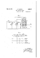
- Fig. 1 diagrammatically shows a circuit including a pair of high permeability transformers connected in the output circuit of a ⁇ multi-stage vacuum tube amplifier, whereof -the secondary windings are connected through separate rectiers to a common feedback circuit; I l
- Fig. 2 represents the signal current in the S5 produce a secondary yimpulse primaryy windings, the corresponding voltage impulses in the secondary windings and the correction impulses fed back to the amplifier for the arrangement shown in Fig. 1;
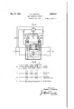
- Fig. 3 shows a modification of Fig. 1 wherein rectifiers of the three-element electron dischar e type are arranged toq cooperate with an osclllator and a 'pair of oscillating windings .on the transformer for effecting zero wander correction;
- Fig. 4 represents a signal current wave and the secondary, rectified and correcting impulse waves produced by the arrangement of ig. 3; ⁇ t
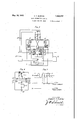
- Fig. 5 illustrates a modification of Fig.
- batteries are used to furnish cur- Gli rent for the plate circuits of the rectifiers;
- Fig. 6 illustrates the high permeability transformers connected in a circuit designed to indicate zero wander effect
- the intervals during which the secondary impulses occur may be changed to include any particulargrange of signaling current amplitdes, by employing additional windings 17 and 18 and by applying thereto opposite biasing currents of such value that the transformer cores may be maintained magnetically saturated during the time that the signaling current is rislng from zero value to theparticular value at which the mag-neto.
- the biasingcurrent is furnished from a source 19 of direct current and is arranged to iiowv in opposite directions through the windings 17 and 18. In this way the inductance of the primary windings is negligible up to the point where the magnetomotive force of the signaling current overcomes that of the biasing currentin either of' windings 17 and 18 and then the inductance rapidly rises to a high value where it.
- ⁇ is effective to produce a short sharp impulse in one or the other of the secondary-windings 15 and 16, the winding selected, dependingupon the polarity of the signaling current impulse owing at the time in theprimary: windings 12 and 13.
- the biasing current is given such value as tov maintain the transformer cores saturated until the signaling current rises to an amplitude indicated by the broken line X-X which represents the normal peak value .of the signaling current on the positive side, a corresponding lineY-Y being shown to represent the normal peak value of thesignaling current on the negative side.
- Curve D represents the discharge of condenser 24, which discharge is impressed on the grid of amplier 25 to restore the zero of th sig- ⁇ naling current to its correct position, as incondenser 27.
- the rectified impulses may be impressed through the resistance-capacity filter comprising resistance elements 28 and 29, and condenser 24 on the grid of amplifier 25 in the manner hereinbefore described and correction in'the opposite direction would thereby be effected.
- Fig. 3 shows another form of a zero corrector whereby high permeability transformers are employed for producing secondary voltage impulses and for impressing such impulses on the grid lcircuit of an amplifier i Y to restore the zero of the signaling current to its true position.
- a vacuum tube ampliiier 31 is connected through the primary windings 32 and 33 of a pair of high permeability ⁇ transformers to a receiving circuit 34.
- Coils 35 and 36 are the secondary windings and coils 37 and 38 are the oppositely oled biasing windingsythe latter windings eing furnished with direct current from source 39.
- Respectively connected in the circuit of the secondary windings 35 and 36. are rectiiiers 40 and 41 of a vacuum tube type.
- An additional pair of windings 42 and 43 are provided on the transformer cores and are connected to an oscillator 44 which is designed to deliver a current of small amplitude at ⁇ about 200 cycles per second or other suitable frequency.
- the oscillator current passing through -the windings 42 and 43 causes a series of correction pulses to be produced in the active wind- .by the biasing current in either ofwthe wind-l ings 37 and 38.
- Curve G represents the rectiiied impulses of curve F received ascharges on storing condenser 45.
- Curve H is the voltage wave discharge from condenser 45 of the filter network and impressed over the feedback circuit 47 on the grid of a vacuum tube (not shown) of amplifier 31.
- Thecorrection impulse received from condenser 45y is eii'eetive in 'restoring the zero wander ofthe signaling current to its true positionz as shown in the trace of curve E.
- the oscillator current is utilized for furnishing current for the filament and the plate circuits of both rectiers, the rectifier associated with the secondary winding which4 happens to be active at the time, receiving the current.
- Fig. 5 shows still another form of zero corrector, in which high permeability trans- -formers are employed, which is quite similar to that shown in Fig. 3, ⁇ llike parts being designated by the same numerals.
- a difference between Fig. 3 and Fig. 5 is that separate batteries are furnished for the plate clrcuits of rectiiers 40 and 41 and for changing the storing condenser 45.
- Fi 6 shows a circuit arrangement in whic a pair of high permeability transform- .ers are employed in conjunction with an indicator for indicating when the zero of the signaling current wanders from its true position.
- an indicator for indicating when the zero of the signaling current wanders from its true position.
- the biasing'current from source 55 is regulated by an adjustable resistance 56 to vmaintain the transformer ⁇ cores saturated up to the normal peak value of the signaling current.
- the magnetic field set up by the biasing current is neutralized and a voltage impulse is produced in either of the secondary windings 57 and 58, the windings selected, as stated above, depending on the polarity of the signaling current.
- An indicator such as a telephone receiver 60 in.
- Fig. 7 is shown an illustration of the operation of the circuit arrangement of Fig. 6.
- Curve K shows a distorted signal current wave passing through the primary windings 51 and 52 with its apparent zero shifting toward the positive side, lines X-X and Y-Y indicating the normal peak values 8f the signaling current.
- Curve L shows the impulses produced in one of the secondary windings 57 or 58, each impulse being heard in the form lof a sharp click in th telephone receiver as the signal current rises in ⁇ value above the amplitude indicated by line X--X in curve K, whereat it overcomes the magnetic field set up by the biasing current in one of the windings 53 and 54.
- Line M shows the absence of impulses in the other of the secondary windings which indicates that the zero of the signaling current is shifting toward the positive side andthat therefore correction is necessary to establish a balance between the positive and negative si nals.
- sai work circuit being connected to said coil for receiving therefrom .short sharp impulses produced by the reception of a signal wave departmg from the zero axis of impulses by -more than .a normal .maximum amplitude,
- a combination of elements for producing a correction for zero wander comprising an amplifier, -a coil connected to the output circuit of said amfplifier, a biasing source of electromotive orce supplying current for said coil adapted to normally maintain it magnetically biased, a circuit connected to said coil for receivingsliort sharp 'impulses produced by the signal waveimpressed upon said coil, exceeding its normal amplitude and overcoming the biasing current, and means operatively related tosaid last mentioned circuit and controlled by the short sharp impulses for im ressing la voltage on theinput circuit of sai amplifier in opposition to the input voltage.
- means for .correcting zero wander comprising a feedback circuit coupled by 4electrical couplings to the output circuit of said amplifier and connected to the input circuit thereof, devices connected to said couplings for preventing transfer of energy thereby, unless and until the amplified impulses exceed a normal positive or negative value, and means selective in accordance with the sign of impulses exceeding positive or negative values determining the corrective effect of the energy fed back.
- means for correcting zero wander comprising a feed back circuit electrically connected in a fixed state of continuity by electrical couplings to the ⁇ output circuit of 'said amplifier and connected to the input circuit thereof, and devices connected to said cou lings foripreventing transfer of energy tliereby unless and until the amplified impulses exceed a normal positive or negative value.
- an amplifier for increasing the strength of current impulses received from an incoming circuit comprising an input and an output'circuit, a compensating circuit ina fixed state of continuity inductively connected to said output circuit and directly connected to said input circuit, a circuit ⁇ including inductance coilsfor preventing said compensating circuit froxn functioning on signal impulses of normal amplitude, and means in said compensating circuit for impressing on said input circuit, when the incoming signals exfective to prevent the, current in said oscillating circuit from being induced in said com ⁇ pensating circuit until its current exceeds its normal peak values, and means in said compensating circuit .for rectfyin and changing the polarity of said induce voltages to eii'ect correction for distortion in the zero axis of. the signals received in the input circuit.
- a line inductive- 1y connected to said line, and indicating means in said third circuit
- the current in said biasing circuit being arranged to lprevent inductive coupling between said line and said third circuit until the incoming signal current exceeds. its normal peak values at which time the inductive coupling suddenly rises toa high ⁇ -value and produces voltage impulses in said third circuit to operate said indicating means.
- a device for correcting the zero Wander eiect in received signals of varying amplitudes comprising an amplifier, a plurality of coils connected to the output circuit of said ampliiier,I said coils having core material of high permeability at low magnetizing forces, a pluralit of other coils respectively connected to the rst mentioned coils, a source of current connected to said second mentioned coil to normally maintain the cores of said first mentioned coils magnetically -saturated in opposite directions when the signaling current in said iirst mentioned coils is passing through amplitudes between zero and its normal peak value, a plurality of circuits respectively concluding another coil, a rectier and an energyl nected to said rst mentioned coils,veach intransferring element, wherein voltage impulses of opposite polarities are produced every time the current in the first mentioned coils rises and falls through its normal peak values, and means connected .in common to.
- said plurality of circuits lfor utilizing said voltage impulses to produce opposing eiects upon the signaling current in the input circuit of said amplifier.
Landscapes
- Engineering & Computer Science (AREA)
- Power Engineering (AREA)
- Computer Networks & Wireless Communication (AREA)
- Signal Processing (AREA)
- Magnetic Resonance Imaging Apparatus (AREA)
Description
May l0, 1932. E. T. BURTON 1,858,037
v ZERO QORRECTING CIRCUIT I V Filed July 19, 1528 3 sheets-Sheet 2 /NVE/vrm [vtm-Tr 7.' BURTON May l0, 1932. E. T. BURTON 1,858,037
' zERo'coRREcTING CIRCUIT Fi1edJu1y'19,192a sheets-Sheet 5 4/ -III Illlll www @am www] um Y 42 bmw I 4J del .M255
0/- AMP. 0,40 Tj! I X n l l l UWT-T1 g I A f +.5/DE I: Y Y PHO/vf CURRENT l i l I l l -J/of l l' I PHO/vf CUR/mw Patented May 10, 1932 I u UNITED sTATEs PATENT l oFFIc-E 'EVERETT T. BURTON, OF MILLBURN, NEW JERSEY, .ASSIGNOR TO BELL TELEPHONE LABORATORIES, INCORPORATED, OF NEW YORK, N. Y., A CORPORATION OFNEW Yom:
ZERO CORRECTING CIRCUIT Application led I.Tuly 19,
This invention relates to si nal transmission systems and more particu arlyto receiving systems for use in connection with submarine cables or other high capacity conductors.
One j object is to correct for the effect known'as zero wander in a highly efficacious A feature of the invention is the use of high permeability inductance coils in combination with suitable circuit arrangements to eii'ect the correction. A v,
It is well known in the art that signaling over high capacity cables, such as submarme cables, by means of positive and negative impulses, earth currents or a temporary preponderance of impulses of one polarity will cause an accumulative 'charging effect 1n the cable which manifests itself as an apparent shifting of the zero line in the direction of the impulse, which, for the time being, predominates. The distorted signal wave arriving at the receiving end of the cable may, in other words, be said to consist of two components; one, the high frequency current refversals sent out by the transmitting station, and the other a low frequency variation, representing the fluctuating charge on the cable following the momentary preponderance of impulses of one or the other polarity.
When the receiving apparatus is a s iphon recorder, the shifting of the zero, oras is commonly/called, zero wander, isof relatively minor importance, but when relays are to be operated it becomes essential to limit the amplitude of zero wander effect-s to a rather small ,proportion of the total signal impulse amplitude. If the shifting of the zero becomes more than 20 lper cent of the normal -signal amplitude the current in the relay windings of the receiving circuit may not be suiiicient to move the armatures of the relays into engagement with both contacts and the relays will fail to'operate, thus rendering the signals unintelligible. y
In the case of printing telegraph systems where the apparatus at the opposite ends of the cable must be held in synchronism, the uncertainty ofthe operation of relays caused by zero wander, in turn causes serious varia- 192s. serial no. 293,816.
tion in synchronism and may-make operation im ossible.
ccording to the present invention the corductance thereof rises for an instant to a y high value thereby producing short'voltage/ impulses in the secondary windings. By adding biasing windings to the transformers and. applying equal and opposite currents to these windings the transformer cores may be made to become saturated at a higher amplitude and the result is to shift the point from near the zero value of the primary .current at-which the secondary impulses occur L to the position where the magneto-motive force of the primary current is equaland opposite to that of the current in either biasing windings. By adj nsting the biasing currents to change the positionat which the sum of the magneto-motive forces is `equal to zero, to the normal peak values 0f the primary current, any signal which exceedsthese normal peak values will which is change in polarity and impressed on the primary current to restore the appar- `ent zero to its true. position.
The invention will be described in connection with the accompanying drawings, in.
Fig. 1 diagrammatically shows a circuit including a pair of high permeability transformers connected in the output circuit of a `multi-stage vacuum tube amplifier, whereof -the secondary windings are connected through separate rectiers to a common feedback circuit; I l
Fig. 2 represents the signal current in the S5 produce a secondary yimpulse primaryy windings, the corresponding voltage impulses in the secondary windings and the correction impulses fed back to the amplifier for the arrangement shown in Fig. 1;
Fig. 3 shows a modification of Fig. 1 wherein rectifiers of the three-element electron dischar e type are arranged toq cooperate with an osclllator and a 'pair of oscillating windings .on the transformer for effecting zero wander correction; i
Fig. 4 represents a signal current wave and the secondary, rectified and correcting impulse waves produced by the arrangement of ig. 3;` t
Fig. 5 illustrates a modification of Fig.; 3
wherein batteries are used to furnish cur- Gli rent for the plate circuits of the rectifiers;
Fig. 6 illustrates the high permeability transformers connected in a circuit designed to indicate zero wander effect; and
saturated at the low amplitudes ofthe signaling current flowing in the output circuit of amplifier '11.- In the absence of blasmg windings or biasing current it is during the,
interval in which the signaling current isrising through the very low amplitudes that the .inductance of the primary windings would be caused to rise to a high value to thereby produce a short sharp impulse in the secondary windings and 16. However, the intervals during which the secondary impulses occur may be changed to include any particulargrange of signaling current amplitdes, by employing additional windings 17 and 18 and by applying thereto opposite biasing currents of such value that the transformer cores may be maintained magnetically saturated during the time that the signaling current is rislng from zero value to theparticular value at which the mag-neto.
motive force of the signalingcurrent overcomes that of the current in either of the biasing windings. The biasingcurrent is furnished from a source 19 of direct current and is arranged to iiowv in opposite directions through the windings 17 and 18. In this way the inductance of the primary windings is negligible up to the point where the magnetomotive force of the signaling current overcomes that of the biasing currentin either of' windings 17 and 18 and then the inductance rapidly rises to a high value where it.
` is effective to produce a short sharp impulse in one or the other of the secondary- windings 15 and 16, the winding selected, dependingupon the polarity of the signaling current impulse owing at the time in theprimary: windings 12 and 13.
Assuming that a signaling current wave flowing in the output circuit of amplifier 11 is distorted and manifests itself as shown by current trace a in curve A of Fig. 2, wherein the apparent shifting of the zero line of the signal is vin a. positive direction, the biasing current is given such value as tov maintain the transformer cores saturated until the signaling current rises to an amplitude indicated by the broken line X-X which represents the normal peak value .of the signaling current on the positive side, a corresponding lineY-Y being shown to represent the normal peak value of thesignaling current on the negative side. Every time the signaling current rises above its normal peak value as indicated by the current trace a, the inductance of the primary winding rises to a' high value, thereby causing an impulse to be produced in either fof' the windings 15 and 16, For the sake of illustration it is assumed that the impulse is produced in winding 16 when the excessive 'signaling current is positive and in winding 15 when the excessive signaling current is negative. Therefore, ac-
cording to curve A an impulseis produced` in winding 16 each time trace a rises above the line X-X. Should the signaling current in rising above its normal peak value rise to such value as to' saturate the transformer cores the inductance again becomes negligible and remains so as vlong as thef core is saturated, but as soon as thescurrentdrops to a value at which the cores become unsatu-zl rated, the inductance of the primary current.
again rises to a high value to produce another impulse in the winding 16 but in the opposite direction. The impulses thus produced, are impressed on the rectifier 20 but only the impulses of one polarity are permitted to pass f and place charges on a storing condenser 21.
Theycharges thus stored are discharged through a resistance-capacity filtervcomprising resistance elements 22 and 23 and condenser 24 to place a ne tive potential on the grid of a vacuum tube 5 of the amplifier 11. The impulses produced in the winding "16 by the rise and fall of' the signaling current through the range of amplitudes slightly above the line X-X are shown in curve B. Curve C represents the impulse wave producedby the discharge of storing condenser 21, wherein the impulses produced by the drop in the primary current are eliminated by rectifier 20 and the impulses produced by the rise of current are inverted for applying correction to the feed-back circuitconnected to the grid of amplifier 25. Curve D represents the discharge of condenser 24, which discharge is impressed on the grid of amplier 25 to restore the zero of th sig- `naling current to its correct position, as incondenser 27. The rectified impulses may be impressed through the resistance-capacity filter comprising resistance elements 28 and 29, and condenser 24 on the grid of amplifier 25 in the manner hereinbefore described and correction in'the opposite direction would thereby be effected.
Fig. 3 shows another form of a zero corrector whereby high permeability transformers are employed for producing secondary voltage impulses and for impressing such impulses on the grid lcircuit of an amplifier i Y to restore the zero of the signaling current to its true position. A vacuum tube ampliiier 31 is connected through the primary windings 32 and 33 of a pair of high permeability `transformers to a receiving circuit 34. Coils 35 and 36 are the secondary windings and coils 37 and 38 are the oppositely oled biasing windingsythe latter windings eing furnished with direct current from source 39. Respectively connected in the circuit of the secondary windings 35 and 36. are rectiiiers 40 and 41 of a vacuum tube type. An additional pair of windings 42 and 43 are provided on the transformer cores and are connected to an oscillator 44 which is designed to deliver a current of small amplitude at `about 200 cycles per second or other suitable frequency. When the signalingl current wanders suiiicently to make one or the other of the secondary windings 35 and .36 active,' the oscillator current passing through -the windings 42 and 43 causes a series of correction pulses to be produced in the active wind- .by the biasing current in either ofwthe wind- l ings 37 and 38. Curve G represents the rectiiied impulses of curve F received ascharges on storing condenser 45. Curve H is the voltage wave discharge from condenser 45 of the filter network and impressed over the feedback circuit 47 on the grid of a vacuum tube (not shown) of amplifier 31. Thecorrection impulse received from condenser 45y is eii'eetive in 'restoring the zero wander ofthe signaling current to its true positionz as shown in the trace of curve E. In thls form of `zero corrector the oscillator current is utilized for furnishing current for the filament and the plate circuits of both rectiers, the rectifier associated with the secondary winding which4 happens to be active at the time, receiving the current. f
Fig. 5 shows still another form of zero corrector, in which high permeability trans- -formers are employed, which is quite similar to that shown in Fig. 3,`llike parts being designated by the same numerals. A difference between Fig. 3 and Fig. 5 is that separate batteries are furnished for the plate clrcuits of rectiiers 40 and 41 and for changing the storing condenser 45.
Fi 6 shows a circuit arrangement in whic a pair of high permeability transform- .ers are employed in conjunction with an indicator for indicating when the zero of the signaling current wanders from its true position. Assuming that primary windings 51 and 52 of a `pair of high permeability transformers are connected to a source (not shown) of signaling current and -that the windings 53 and 54 are connected to a source 55 of direct current in such manner that the transformers are normally maintained biased inA opposite directions, the biasing'current from source 55 is regulated by an adjustable resistance 56 to vmaintain the transformer` cores saturated up to the normal peak value of the signaling current. As soon as the signaling current in this arrangement exceeds its normal peak value, the magnetic field set up by the biasing current is neutralized and a voltage impulse is produced in either of the secondary windings 57 and 58, the windings selected, as stated above, depending on the polarity of the signaling current. An indicator such as a telephone receiver 60 in.
los
series with a small condenser 61 .is arranged creased until the impulses produced in the secondary winding are on the point of disappearing. This is accomplishedby connecting the telephone receiver toeither of the sec-l ondary windings through the operation of switch 62 and by setting the biasing current at a value equal tothe normal peak value of` the signaling current so that a click will be heard in the telephone every time the signaling current rises to its normal peak value on either the positive or the negative side.
Should the current exceed its normal peak value on one side, no click will be heard as the current reaches its peak value on the other side and therefore the unbalanced condition of the signal wave is indicated.
In Fig. 7 is shown an illustration of the operation of the circuit arrangement of Fig. 6. Curve K shows a distorted signal current wave passing through the primary windings 51 and 52 with its apparent zero shifting toward the positive side, lines X-X and Y-Y indicating the normal peak values 8f the signaling current. Curve L shows the impulses produced in one of the secondary windings 57 or 58, each impulse being heard in the form lof a sharp click in th telephone receiver as the signal current rises in `value above the amplitude indicated by line X--X in curve K, whereat it overcomes the magnetic field set up by the biasing current in one of the windings 53 and 54. Line M shows the absence of impulses in the other of the secondary windings which indicates that the zero of the signaling current is shifting toward the positive side andthat therefore correction is necessary to establish a balance between the positive and negative si nals.
7hat is claimed is:
l. In combination with a signal impulse amplifier, a work circuit having a quiescent condition during the reception of impulses of normal maximum amplitude,` a coil connected to the output circuit of the amplifier,
and a biasing source of electromotive force supplying current for said coil adapted to maintaln it magnetically biased up to an intensity equal to that of the normal maximum am litude of the received signal impulses,
sai work circuit being connected to said coil for receiving therefrom .short sharp impulses produced by the reception of a signal wave departmg from the zero axis of impulses by -more than .a normal .maximum amplitude,
and the consequent overcoming of the biasing current of said coil, whereby the quiescent condition of said work circuit is changed to an energized condition.
2; In asignal receiving system, a combination of elements for producing a correction for zero wander comprising an amplifier, -a coil connected to the output circuit of said amfplifier, a biasing source of electromotive orce supplying current for said coil adapted to normally maintain it magnetically biased, a circuit connected to said coil for receivingsliort sharp 'impulses produced by the signal waveimpressed upon said coil, exceeding its normal amplitude and overcoming the biasing current, and means operatively related tosaid last mentioned circuit and controlled by the short sharp impulses for im ressing la voltage on theinput circuit of sai amplifier in opposition to the input voltage.
3. A system in accordance with claim 2 in which the last mentioned circuit includes a rectifier.
4. A system in accordance with claim 2 in which the last mentioned circuitincludes a unidirectional space discharge device and an energy transferring system extending from said device to the input circuit of the y amplifier.
vices` connected to s'aid couplings for pre-I venting transfer of energy thereby, unless and until the amplifier impulses exceed a y normal positive or negative value.
7. In a signal impulse amplifier, means for .correcting zero wander comprising a feedback circuit coupled by 4electrical couplings to the output circuit of said amplifier and connected to the input circuit thereof, devices connected to said couplings for preventing transfer of energy thereby, unless and until the amplified impulses exceed a normal positive or negative value, and means selective in accordance with the sign of impulses exceeding positive or negative values determining the corrective effect of the energy fed back.
8. In a signal impulse amplifier, means for correcting zero wander comprisinga feed back circuit electrically connected in a fixed state of continuity by electrical couplings to the` output circuit of 'said amplifier and connected to the input circuit thereof, and devices connected to said cou lings foripreventing transfer of energy tliereby unless and until the amplified impulses exceed a normal positive or negative value.
9. In a signal'receiving system, an amplifier for increasing the strength of current impulses received from an incoming circuit, comprising an input and an output'circuit, a compensating circuit ina fixed state of continuity inductively connected to said output circuit and directly connected to said input circuit, a circuit `including inductance coilsfor preventing said compensating circuit froxn functioning on signal impulses of normal amplitude, and means in said compensating circuit for impressing on said input circuit, when the incoming signals exfective to prevent the, current in said oscillating circuit from being induced in said com` pensating circuit until its current exceeds its normal peak values, and means in said compensating circuit .for rectfyin and changing the polarity of said induce voltages to eii'ect correction for distortion in the zero axis of. the signals received in the input circuit.
11. In a signal receiving system, a line, a biasing circuit and a third circuit inductive- 1y connected to said line, and indicating means in said third circuit, the current in said biasing circuit being arranged to lprevent inductive coupling between said line and said third circuit until the incoming signal current exceeds. its normal peak values at which time the inductive coupling suddenly rises toa high` -value and produces voltage impulses in said third circuit to operate said indicating means.
12. In a signal receiving system, a device for correcting the zero Wander eiect in received signals of varying amplitudes comprising an amplifier, a plurality of coils connected to the output circuit of said ampliiier,I said coils having core material of high permeability at low magnetizing forces, a pluralit of other coils respectively connected to the rst mentioned coils, a source of current connected to said second mentioned coil to normally maintain the cores of said first mentioned coils magnetically -saturated in opposite directions when the signaling current in said iirst mentioned coils is passing through amplitudes between zero and its normal peak value, a plurality of circuits respectively concluding another coil, a rectier and an energyl nected to said rst mentioned coils,veach intransferring element, wherein voltage impulses of opposite polarities are produced every time the current in the first mentioned coils rises and falls through its normal peak values, and means connected .in common to.
said plurality of circuits lfor utilizing said voltage impulses to produce opposing eiects upon the signaling current in the input circuit of said amplifier.
In witnesswhereof, I hereunto subscribe my name this 16th day of July, 1928.
EVERETT T. BURTON.`
Priority Applications (16)
| Application Number | Priority Date | Filing Date | Title |
|---|---|---|---|
| US293816A US1858037A (en) | 1928-07-19 | 1928-07-19 | Zero correcting circuit |
| GB742629A GB312338A (en) | 1928-05-26 | 1929-03-07 | Improvements in or relating to electrical energy translating systems |
| GB769429A GB312904A (en) | 1928-05-26 | 1929-03-08 | Improvements in electrical telegraph and like signalling systems |
| DEE39029D DE539187C (en) | 1928-05-26 | 1929-03-23 | Power surge transmission system, e.g. for telegraphy |
| DEE39031D DE540413C (en) | 1928-05-26 | 1929-03-26 | Method of signaling using inductance transformer coils |
| FR673502D FR673502A (en) | 1928-05-26 | 1929-04-18 | Transmission system |
| FR36770D FR36770E (en) | 1928-05-26 | 1929-04-25 | Transmission systems |
| GB1552029A GB315821A (en) | 1928-05-26 | 1929-05-17 | Improvements in amplifiers for telegraphic and like signals |
| DE1929E0039267 DE540412C (en) | 1928-05-26 | 1929-05-18 | Arrangement for correcting the zero line in telegraphic receiving stations with amplifiers |
| FR37104D FR37104E (en) | 1928-05-26 | 1929-05-31 | Transmission system |
| GB1951829A GB318989A (en) | 1928-05-26 | 1929-06-25 | Improvements in receivers for telegraphic and like signals |
| DE1929E0039570 DE553928C (en) | 1928-05-26 | 1929-07-14 | Process for the automatic correction of the zero line in telegraphic systems with receiving amplifiers and with pulse transmitter coils |
| FR37685D FR37685E (en) | 1928-05-26 | 1929-07-31 | Transmission systems |
| GB28990/29A GB340286A (en) | 1928-05-26 | 1929-09-24 | Improvements in electrical frequency changing apparatus |
| US490585A US2039629A (en) | 1928-05-26 | 1930-10-23 | Telegraph repeater |
| GB28413/31A GB390542A (en) | 1928-05-26 | 1931-10-13 | Improvements in or relating to electrical signalling systems |
Applications Claiming Priority (1)
| Application Number | Priority Date | Filing Date | Title |
|---|---|---|---|
| US293816A US1858037A (en) | 1928-07-19 | 1928-07-19 | Zero correcting circuit |
Publications (1)
| Publication Number | Publication Date |
|---|---|
| US1858037A true US1858037A (en) | 1932-05-10 |
Family
ID=23130702
Family Applications (1)
| Application Number | Title | Priority Date | Filing Date |
|---|---|---|---|
| US293816A Expired - Lifetime US1858037A (en) | 1928-05-26 | 1928-07-19 | Zero correcting circuit |
Country Status (1)
| Country | Link |
|---|---|
| US (1) | US1858037A (en) |
Cited By (3)
| Publication number | Priority date | Publication date | Assignee | Title |
|---|---|---|---|---|
| US2462470A (en) * | 1943-06-17 | 1949-02-22 | Rca Corp | Telegraphy receiver with automatic frequency control |
| US2958827A (en) * | 1943-09-02 | 1960-11-01 | Warren A Anderson | Electrical cancellation and indicating system |
| US3210557A (en) * | 1960-05-10 | 1965-10-05 | Philips Corp | Device for checking the presence or absence of a plurality of direct currents |
-
1928
- 1928-07-19 US US293816A patent/US1858037A/en not_active Expired - Lifetime
Cited By (3)
| Publication number | Priority date | Publication date | Assignee | Title |
|---|---|---|---|---|
| US2462470A (en) * | 1943-06-17 | 1949-02-22 | Rca Corp | Telegraphy receiver with automatic frequency control |
| US2958827A (en) * | 1943-09-02 | 1960-11-01 | Warren A Anderson | Electrical cancellation and indicating system |
| US3210557A (en) * | 1960-05-10 | 1965-10-05 | Philips Corp | Device for checking the presence or absence of a plurality of direct currents |
Similar Documents
| Publication | Publication Date | Title |
|---|---|---|
| US2703368A (en) | Pulse regeneration | |
| US1921022A (en) | Submarine cable signaling system | |
| US1858037A (en) | Zero correcting circuit | |
| US3476879A (en) | Line relay for d.c. telegraph systems | |
| US1477017A (en) | Current-controlling and static-reducing system | |
| US1959459A (en) | Frequency changing system | |
| US2701276A (en) | Twinplex telegraph signal receiver | |
| US1836574A (en) | Signal shaping amplifier | |
| US1863674A (en) | Means for reducing lightning interference in carrier telegraph circuits | |
| US2294735A (en) | Carrier current amplifier apparatus | |
| US2248857A (en) | Automatic bias corrector | |
| US1537682A (en) | Telegraphic receiving system | |
| US2147688A (en) | Magnetic impulse storing device | |
| US1818463A (en) | Zero correcting circuit | |
| US2345881A (en) | Correction of distorted telegraph signals | |
| US2044062A (en) | Impulse telegraph repeater | |
| US3071655A (en) | Time division junction circuit for a transmission line | |
| US1875935A (en) | Dot insertion | |
| US1763880A (en) | Signaling system | |
| US2101256A (en) | Carrier telegraph receiver | |
| US1673697A (en) | Relay and relaying system | |
| US1832722A (en) | Shaping arrangement for metallic telegraph circuits | |
| US1584684A (en) | Duplex system of telegraphy | |
| US1809722A (en) | Superposed telegraph system | |
| US1811824A (en) | Vacuum tube repeater and terminal set for superposed telegraph systems |