US12356071B2 - Optical element driving mechanism - Google Patents

Optical element driving mechanism Download PDF

Info

Publication number
US12356071B2
US12356071B2 US17/553,126 US202117553126A US12356071B2 US 12356071 B2 US12356071 B2 US 12356071B2 US 202117553126 A US202117553126 A US 202117553126A US 12356071 B2 US12356071 B2 US 12356071B2
Authority
US
United States
Prior art keywords
optical element
optical
movable part
driving mechanism
axis
Prior art date
Legal status (The legal status is an assumption and is not a legal conclusion. Google has not performed a legal analysis and makes no representation as to the accuracy of the status listed.)
Active, expires
Application number
US17/553,126
Other versions
US20220196974A1 (en
Inventor
Shu-Shan Chen
Chao-Chang Hu
Chih-Wei Weng
Current Assignee (The listed assignees may be inaccurate. Google has not performed a legal analysis and makes no representation or warranty as to the accuracy of the list.)
TDK Taiwan Corp
Original Assignee
TDK Taiwan Corp
Priority date (The priority date is an assumption and is not a legal conclusion. Google has not performed a legal analysis and makes no representation as to the accuracy of the date listed.)
Filing date
Publication date
Application filed by TDK Taiwan Corp filed Critical TDK Taiwan Corp
Priority to US17/553,126 priority Critical patent/US12356071B2/en
Assigned to TDK TAIWAN CORP. reassignment TDK TAIWAN CORP. ASSIGNMENT OF ASSIGNORS INTEREST (SEE DOCUMENT FOR DETAILS). Assignors: CHEN, SHU-SHAN, HU, CHAO-CHANG, WENG, CHIH-WEI
Publication of US20220196974A1 publication Critical patent/US20220196974A1/en
Priority to US19/237,320 priority patent/US20250310645A1/en
Application granted granted Critical
Publication of US12356071B2 publication Critical patent/US12356071B2/en
Active legal-status Critical Current
Adjusted expiration legal-status Critical

Links

Images

Classifications

    • HELECTRICITY
    • H04ELECTRIC COMMUNICATION TECHNIQUE
    • H04NPICTORIAL COMMUNICATION, e.g. TELEVISION
    • H04N23/00Cameras or camera modules comprising electronic image sensors; Control thereof
    • H04N23/60Control of cameras or camera modules
    • H04N23/68Control of cameras or camera modules for stable pick-up of the scene, e.g. compensating for camera body vibrations
    • H04N23/682Vibration or motion blur correction
    • H04N23/685Vibration or motion blur correction performed by mechanical compensation
    • H04N23/687Vibration or motion blur correction performed by mechanical compensation by shifting the lens or sensor position
    • GPHYSICS
    • G02OPTICS
    • G02BOPTICAL ELEMENTS, SYSTEMS OR APPARATUS
    • G02B13/00Optical objectives specially designed for the purposes specified below
    • G02B13/001Miniaturised objectives for electronic devices, e.g. portable telephones, webcams, PDAs, small digital cameras
    • G02B13/0015Miniaturised objectives for electronic devices, e.g. portable telephones, webcams, PDAs, small digital cameras characterised by the lens design
    • GPHYSICS
    • G02OPTICS
    • G02BOPTICAL ELEMENTS, SYSTEMS OR APPARATUS
    • G02B26/00Optical devices or arrangements for the control of light using movable or deformable optical elements
    • GPHYSICS
    • G02OPTICS
    • G02BOPTICAL ELEMENTS, SYSTEMS OR APPARATUS
    • G02B26/00Optical devices or arrangements for the control of light using movable or deformable optical elements
    • G02B26/08Optical devices or arrangements for the control of light using movable or deformable optical elements for controlling the direction of light
    • G02B26/0875Optical devices or arrangements for the control of light using movable or deformable optical elements for controlling the direction of light by means of one or more refracting elements
    • GPHYSICS
    • G02OPTICS
    • G02BOPTICAL ELEMENTS, SYSTEMS OR APPARATUS
    • G02B27/00Optical systems or apparatus not provided for by any of the groups G02B1/00 - G02B26/00, G02B30/00
    • G02B27/64Imaging systems using optical elements for stabilisation of the lateral and angular position of the image
    • G02B27/646Imaging systems using optical elements for stabilisation of the lateral and angular position of the image compensating for small deviations, e.g. due to vibration or shake
    • GPHYSICS
    • G02OPTICS
    • G02BOPTICAL ELEMENTS, SYSTEMS OR APPARATUS
    • G02B7/00Mountings, adjusting means, or light-tight connections, for optical elements
    • G02B7/02Mountings, adjusting means, or light-tight connections, for optical elements for lenses
    • G02B7/04Mountings, adjusting means, or light-tight connections, for optical elements for lenses with mechanism for focusing or varying magnification
    • G02B7/09Mountings, adjusting means, or light-tight connections, for optical elements for lenses with mechanism for focusing or varying magnification adapted for automatic focusing or varying magnification
    • GPHYSICS
    • G03PHOTOGRAPHY; CINEMATOGRAPHY; ANALOGOUS TECHNIQUES USING WAVES OTHER THAN OPTICAL WAVES; ELECTROGRAPHY; HOLOGRAPHY
    • G03BAPPARATUS OR ARRANGEMENTS FOR TAKING PHOTOGRAPHS OR FOR PROJECTING OR VIEWING THEM; APPARATUS OR ARRANGEMENTS EMPLOYING ANALOGOUS TECHNIQUES USING WAVES OTHER THAN OPTICAL WAVES; ACCESSORIES THEREFOR
    • G03B13/00Viewfinders; Focusing aids for cameras; Means for focusing for cameras; Autofocus systems for cameras
    • G03B13/32Means for focusing
    • G03B13/34Power focusing
    • G03B13/36Autofocus systems
    • GPHYSICS
    • G03PHOTOGRAPHY; CINEMATOGRAPHY; ANALOGOUS TECHNIQUES USING WAVES OTHER THAN OPTICAL WAVES; ELECTROGRAPHY; HOLOGRAPHY
    • G03BAPPARATUS OR ARRANGEMENTS FOR TAKING PHOTOGRAPHS OR FOR PROJECTING OR VIEWING THEM; APPARATUS OR ARRANGEMENTS EMPLOYING ANALOGOUS TECHNIQUES USING WAVES OTHER THAN OPTICAL WAVES; ACCESSORIES THEREFOR
    • G03B5/00Adjustment of optical system relative to image or object surface other than for focusing
    • GPHYSICS
    • G06COMPUTING OR CALCULATING; COUNTING
    • G06FELECTRIC DIGITAL DATA PROCESSING
    • G06F3/00Input arrangements for transferring data to be processed into a form capable of being handled by the computer; Output arrangements for transferring data from processing unit to output unit, e.g. interface arrangements
    • G06F3/01Input arrangements or combined input and output arrangements for interaction between user and computer
    • G06F3/016Input arrangements with force or tactile feedback as computer generated output to the user
    • HELECTRICITY
    • H04ELECTRIC COMMUNICATION TECHNIQUE
    • H04NPICTORIAL COMMUNICATION, e.g. TELEVISION
    • H04N23/00Cameras or camera modules comprising electronic image sensors; Control thereof
    • H04N23/50Constructional details
    • H04N23/54Mounting of pick-up tubes, electronic image sensors, deviation or focusing coils
    • HELECTRICITY
    • H04ELECTRIC COMMUNICATION TECHNIQUE
    • H04NPICTORIAL COMMUNICATION, e.g. TELEVISION
    • H04N23/00Cameras or camera modules comprising electronic image sensors; Control thereof
    • H04N23/57Mechanical or electrical details of cameras or camera modules specially adapted for being embedded in other devices
    • HELECTRICITY
    • H10SEMICONDUCTOR DEVICES; ELECTRIC SOLID-STATE DEVICES NOT OTHERWISE PROVIDED FOR
    • H10NELECTRIC SOLID-STATE DEVICES NOT OTHERWISE PROVIDED FOR
    • H10N30/00Piezoelectric or electrostrictive devices
    • H10N30/101Piezoelectric or electrostrictive devices with electrical and mechanical input and output, e.g. having combined actuator and sensor parts
    • HELECTRICITY
    • H10SEMICONDUCTOR DEVICES; ELECTRIC SOLID-STATE DEVICES NOT OTHERWISE PROVIDED FOR
    • H10NELECTRIC SOLID-STATE DEVICES NOT OTHERWISE PROVIDED FOR
    • H10N30/00Piezoelectric or electrostrictive devices
    • H10N30/80Constructional details
    • H10N30/802Circuitry or processes for operating piezoelectric or electrostrictive devices not otherwise provided for, e.g. drive circuits

Definitions

  • the present disclosure relates to an optical element driving mechanism, and more particularly to an optical element driving mechanism of an electrical device.
  • an optical element driving mechanism including a first movable part, a second movable part, and a third movable part.
  • the first movable part is connected to a first optical element.
  • the second movable part is connected to a second optical element including an optical axis.
  • the third movable part is connected to a third optical element.
  • the first optical element, the second optical element, and the third optical element are arranged along the optical axis.
  • the second optical element is located between the first optical element and the third optical element when viewed along a direction that is perpendicular to the optical axis.
  • the first optical element is not in contact with the second optical element when the first movable part limiting element is in contact with the second movable part limiting element.
  • the fourth optical element has a fourth optical element top side and a fourth optical element bottom side opposite to the fourth optical element top side.
  • the fourth optical element bottom side faces the first optical element.
  • the area of the fourth optical element top side is larger than the area of the fourth optical element bottom side.
  • the optical element driving mechanism further includes a fixed part.
  • the fixed part includes a frame
  • the movable part includes a third optical element holder.
  • the frame accommodates the second movable part
  • the third optical element holder accommodates the third optical element.
  • the first supporting element is movable along a first axis that is perpendicular to the optical axis.
  • the first supporting element is movable along a first axis that is perpendicular to the optical axis and a second axis that is perpendicular to the optical axis and the first axis.
  • the optical element driving mechanism further includes a second supporting element.
  • the second supporting element is located between the third optical element holder and the bottom plate.
  • the optical element driving mechanism further includes a first supporting element and an elastic assembly.
  • the frame is in contact with the elastic assembly.
  • the first supporting element is connected to the elastic assembly, and the first supporting element is connected to the third optical element holder.
  • the frame is not in direct contact with the third optical element holder.
  • the first optical element is in active alignment with the second optical element
  • the second optical element is m active alignment with the third optical element
  • the fourth optical element is in active alignment with the second optical element
  • the optical element driving mechanism further includes a fixed part.
  • the fixed part includes an outer frame, and the outer frame includes an outer frame top surface opening. A fourth optical element top side of the fourth optical element is exposed to the outer frame top surface opening.
  • the optical element driving mechanism further includes a fixed part.
  • the fixed part includes an outer frame
  • the outer frame includes an outer frame sidewall opening.
  • a first circuit element that controls the first movable part is exposed to the outer frame sidewall opening.
  • the optical element driving mechanism further includes a fixed part.
  • the fixed part includes an outer frame, and the outer frame includes an outer frame sidewall recess.
  • a third circuit element that controls the third optical element is exposed to the outer frame sidewall recess.
  • the optical element driving mechanism further includes a first driving assembly, and a second driving assembly.
  • the first driving assembly drives the first optical element to control the amount of the incident light.
  • the second driving assembly drives the second movable part to move relative to the fixed part.
  • the fixed part has a polygonal structure when viewed along a direction that is parallel to the optical axis.
  • the first driving assembly and the second driving assembly are located at different sides of the fixed part.
  • the first driving assembly includes a first driving magnetic element
  • the second driving assembly includes a second driving magnetic element.
  • the fixed part includes a first side, a second side, and a fourth side.
  • the second side is parallel to the fourth side, and the first side is not parallel to the second side.
  • the first driving magnetic element is disposed on the first side
  • the second driving magnetic element is disposed on the second side and the fourth side.
  • the optical element driving mechanism further includes a third driving assembly.
  • the third driving assembly drives the third movable part to move relative to the fixed part.
  • the first driving assembly and the third driving assembly are located on different sides of the fixed part.
  • FIG. 1 is a schematic view of an electrical device according to some embodiment of the present disclosure.
  • FIG. 2 is a schematic view of the optical element driving mechanism according to some embodiments of the present disclosure, wherein the outer frame is shown as a dashed line.
  • FIG. 3 is an exploded view of the optical element driving mechanism according to some embodiments of the present disclosure.
  • FIG. 4 is a cross-sectional view of the optical element driving mechanism along line A-A′ of FIG. 2 , according to some embodiments of the present disclosure.
  • FIG. 5 is a cross-sectional view of the optical element driving mechanism along line B-B′ of FIG. 2 , according to some embodiments of the present disclosure.
  • FIG. 6 is a schematic view of an optical element driving mechanism according to some embodiments of the present disclosure, wherein the outer frame is shown as a dashed line.
  • FIG. 7 is an exploded view of the optical element driving mechanism according to some embodiments of the present disclosure.
  • optical element driving mechanisms of embodiments of the present disclosure are discussed in detail below. It should be appreciated, however, that the embodiments provide many applicable inventive concepts that may be embodied in a wide variety of specific contexts. The specific embodiments discussed are merely illustrative of specific ways to make and use the embodiments and do not limit the scope of the disclosure.
  • first”, “second” etc. may be used herein to describe various elements, layers and/or portions, and these elements, layers, and/or portions should not be limited by these terms. These terms are only used to distinguish one element, layer, or portion. Thus, a first element, layer or portion discussed below could be termed a second element, layer or portion without departing from the teachings of some embodiments of the present disclosure. In addition, for the sake of brevity, terms such as “first” and “second” may not be used in the description to distinguish different elements. As long as it does not depart from the scope defined by the appended claims, the first element and/or the second element described in the appended claims can be interpreted as any element that meets the description in the specification.
  • FIG. 1 is a schematic view of an electrical device 1 according to some embodiment of the present disclosure.
  • an optical element driving mechanism 100 of some embodiment of the present disclosure may be mounted in an electrical device 1 for taking photos or videos, wherein the aforementioned electrical device 1 may, for example, be a smartphone or a digital camera, but the present disclosure is not limited to these.
  • the position and the size between the optical element driving mechanism 100 and the electrical device 1 shown in FIG. 1 are only an example, which is not for limiting the position and the size between the optical element driving mechanism 100 and the electrical device 1 .
  • the optical element driving mechanism 100 may be mounted at different positions in the electrical device 1 .
  • FIG. 2 is a schematic view of the optical element driving mechanism 100 according to some embodiments of the present disclosure, wherein the outer frame is shown as a dashed line.
  • FIG. 3 is an exploded view of the optical element driving mechanism 100 according to some embodiments of the present disclosure.
  • the optical element driving mechanism 100 may include a fixed part 10 , a first movable part 20 , a second movable part 25 , a third movable part 30 , and a first driving assembly 35 , a second driving assembly 40 , a third driving assembly 45 , a supporting assembly 50 , an elastic assembly 55 , a circuit assembly 60 , a first optical element 65 , a second optical element 70 , a third optical element 75 , and a fourth optical element 80 .
  • the second optical element 70 may have an optical axis O.
  • the fixed part 10 may include an outer frame 11 , a bottom plate 12 , and a frame 13 .
  • the outer frame 11 may be disposed on the bottom plate 12 to form an internal space.
  • the frame 13 is disposed in the internal space.
  • the fixed part 10 has a polygonal structure when viewed along a direction that is parallel to the optical axis O.
  • the fixed part 10 may have a first side 10 a , a second side 10 b , a third side 10 c , and a fourth side 10 d.
  • the first side 10 a may be parallel to the third side 10 c .
  • the second side 10 b may be parallel to the fourth side 10 d .
  • the first side 10 a may not be parallel to the second side 10 b and the fourth side 10 d.
  • the outer frame 11 may include an outer frame top surface opening 111 , an outer frame sidewall opening 112 , and an outer frame sidewall recess 113 .
  • the outer frame top surface opening 111 is located on the top surface of the outer frame 11
  • the outer frame sidewall opening 112 and the outer frame sidewall recess 113 are located on the sidewall of the outer frame.
  • the outer frame sidewall opening 112 and the outer frame sidewall recess 113 may be located on different sides.
  • the outer frame sidewall opening 112 may be located on the first side 10 a of the fixed part 10
  • the outer frame sidewall recess 113 may be located on the second side 10 b of the fixed part 10 .
  • the first driving assembly 35 and the third driving assembly 45 may be disposed on different sides of the fixed part 10 .
  • the third driving magnetic element 46 and the third driving coil 47 of the third driving assembly 45 may be disposed on the second side 10 b , the third side 10 c , and the fourth side 10 d of the fixed part 10 ; however, the first side 10 a of the fixed part 10 where the first driving magnetic element 36 and the first driving coil 37 of the first driving assembly 35 is provided is not provided with the third driving magnetic element 46 and the third driving coil 47 of the third driving assembly 45 .
  • the interaction of the first driving assembly 35 , the second driving assembly 40 , and the third driving assembly 45 may be minimized, so that the control of the first driving assembly 35 , the second driving assembly 40 , and the third driving assembly 45 may be more precise.
  • the third driving coil 47 may be disposed corresponding to the second driving magnetic element 41 , so as to share the second driving magnetic element 41 with the second driving coil 42 . In this way, it may be helpful for miniaturizing the optical element driving mechanism 100 .
  • the supporting assembly 50 may include a first supporting element 51 and a second supporting element 52 .
  • the elastic assembly 55 may include a first elastic element 56 and a second elastic element 57 .
  • the circuit assembly 60 may include a first circuit element 61 , a second circuit element (not shown), and a third circuit element 63 .
  • the first circuit element 61 may control the first driving assembly 35 by receiving an external current, thereby controlling and driving the first movable part 20 and the first optical element 65 .
  • the second circuit element (not shown) may control the second driving assembly 40 by receiving an external current, thereby controlling and driving the second movable part 25 and the second optical element 70 .
  • the third circuit element 63 may control the third driving assembly 45 by receiving an external current, thereby controlling and driving the third movable part 30 and the third optical element 75 .
  • the first circuit element 61 may be exposed to the outer frame sidewall opening 112 .
  • the third circuit element 63 may be exposed to the outer frame sidewall recess 113 .
  • the first optical element 65 may be an aperture, a shutter, or the like.
  • the second optical element 70 may be a lens.
  • the third optical element 75 may be a photosensitive element.
  • the fourth optical element 80 may be a lens. It should be noted that the first optical element 65 , the second optical element 70 , the third optical element 75 , and the fourth optical element 80 are not limited to the examples described herein. In fact, suitable optical elements may be selected according to requirements.
  • the first optical element 65 is in active alignment (AA) with the second optical element 70 .
  • the second optical element 70 is in active alignment with the third optical element 75 .
  • the fourth optical element 80 is in active alignment with the second optical element 70 . In this way, the image quality may be stabilized, and the image quality may be improved.
  • the first driving assembly 35 may drive the first movable part 20 and the first optical element 65 , so as to control the amount of incident light that incident to the second optical element 70 .
  • the second driving assembly 40 may drive the second movable part 25 and the second optical element 70 to move along the optical axis O relative to the fixed part 10 .
  • the third driving assembly 45 may drive the third movable part 30 to move relative to the fixed part 10 along the first axis AX 1 that is perpendicular to the optical axis O and/or the second axis AX 2 that is perpendicular to the optical axis O and the first axis AX 1 .
  • FIG. 4 is a cross-sectional view of the optical element driving mechanism 100 along line A-A′ of FIG. 2 , according to some embodiments of the present disclosure.
  • the first optical element holder 21 of the first movable part 20 may be connected to the first optical element 65 .
  • the second optical element holder 26 of the second movable part 25 may be connected to the second optical element 70 .
  • the third optical element holder 31 of the third movable part 30 may be connected to the third optical element 75 .
  • the outer frame 11 of the fixed part 10 may be connected to the fourth optical element 80 .
  • the first optical element 65 , the second optical element 70 , the third optical element 75 , and the fourth optical element 80 are arranged along the optical axis O.
  • the first optical element 65 is located between the second optical element 70 and the fourth optical element 80 when viewed along the first axis AX 1 and/or the second axis AX 2 that are perpendicular to the optical axis O.
  • the second optical element 70 is located between the first optical element 65 and the third optical element 75 when viewed along the first axis AX and/or the second axis AX 2 that are perpendicular to the optical axis O.
  • the first optical element holder 21 of the first movable part 20 may have a first movable part limiting element 211
  • the second optical element holder 26 of the second movable part 25 may have a second movable part limiting element 261 .
  • the shortest distance S 1 between the first movable part limiting element 211 and the second movable part limiting element 261 is shorter than the shortest distance S 2 between the first optical element 65 and the second optical element 70 when viewed along the first axis AX 1 and/or the second axis AX 2 that are perpendicular to the optical axis O.
  • the first optical element 65 is not in contact with the second optical element 70 when the first movable part limiting element 211 is in contact with the second movable part limiting element 261 .
  • the first optical element 65 is avoided from contacting the second optical element 70 , and thus the damage of the first optical element 65 and the second optical element 70 is avoided.
  • the elastic assembly 55 may connect the first optical element holder 21 of the first movable part 20 and the second optical element holder 26 of the second movable part 25 to the frame 13 of the fixed part 10 .
  • the first elastic element 56 of the elastic assembly 55 may connect the first optical element holder 21 to the upper part of the frame 13
  • the second elastic element 57 of the elastic assembly 55 may connect the second optical element holder 26 to the lower part of the frame 13 .
  • first optical element holder 21 and the second optical element holder 26 may be supported, and the second optical element holder 26 may move relative to the frame 13 along the optical axis O.
  • the fourth optical element 80 has a fourth optical element top side 80 a and a fourth optical element bottom side 80 b .
  • the fourth optical element top side 80 a of the fourth optical element 80 is exposed to the outer frame top surface opening 111 of the outer frame 11 to receive light from the outside.
  • the fourth optical element bottom side 80 b is opposite to the fourth optical element top side 80 a , that is, the fourth optical element top side 80 a and the fourth optical element bottom side 80 b face different directions.
  • the fourth optical element bottom side 80 b faces the first optical element 65 .
  • the area of the fourth optical element bottom side 80 b is larger than the area of the fourth optical element bottom side 80 b . In this way, the amount of the light that enters the fourth optical element 80 may be increased, and the imaging quality may be improved.
  • the second optical element 70 has a second optical element top side 70 a and a second optical element bottom side 70 b .
  • the second optical element bottom side 70 b is opposite to the second optical element top side 70 a , that is, the second optical element top side 70 a and the second optical element bottom side 70 b face different directions.
  • the frame 13 accommodates the second optical element holder 26 of the second movable part 25
  • the third optical element holder 31 accommodates the third optical element 75 .
  • the position of the third optical element 75 may be adjusted to improve the imaging quality.
  • the third optical element holder 31 is located between the frame 13 and the bottom plate 12 .
  • the second supporting element 52 may be a sphere.
  • the second supporting element 52 may be located between the third optical element holder 31 and the bottom plate 12 , so that the third optical element holder 31 is not in direct contact with the bottom plate 12 . In this way, the third optical element holder 31 may move relative to the bottom plate 12 .
  • the second supporting element 52 may move along the first axis AX 1 . According to some embodiments of the present disclosure, the second supporting element 52 may move along the second axis AX 2 . According to some embodiments of the present disclosure, the second supporting element 52 may move along the first axis AX 1 and the second axis AX 2 .
  • FIG. 6 is a schematic view of an optical element driving mechanism 200 according to some embodiments of the present disclosure, wherein the outer frame is shown as a dashed line.
  • FIG. 7 is an exploded view of the optical element driving mechanism 200 according to some embodiments of the present disclosure.
  • optical element driving mechanism 200 The main elements and the configuration of the optical element driving mechanism 200 is similar to that of optical element driving mechanism 100 , and the similar parts will not be repeated.
  • the supporting assembly 50 of the optical element driving mechanism 200 may no longer have the second supporting element 52 .
  • the frame 13 is not in direct contact with the third optical element holder 31
  • the bottom plate 12 is not in direct contact with the third optical element holder 31 either.
  • the third optical element holder 31 may move relative to the bottom plate 12 and the frame 13 along the first axis AX 1 and/or the second axis AX 2 , so that the position of the third optical element 75 may be adjusted to improve the imaging quality.
  • the optical element driving mechanism of some embodiments of the present disclosure may adjust the position of the optical element along the optical axis and the directions that are perpendicular to the optical axis, and the amount of incident light that incident to the optical element driving mechanism may be adjusted to improve the imaging quality of the optical element driving mechanism.
  • the optical element driving mechanism of some embodiments of the present disclosure may also be helpful for the optical element driving mechanism to be electrically connected to the outside, and the effect of miniaturization may also be achieved.

Landscapes

  • Physics & Mathematics (AREA)
  • General Physics & Mathematics (AREA)
  • Optics & Photonics (AREA)
  • Engineering & Computer Science (AREA)
  • General Engineering & Computer Science (AREA)
  • Multimedia (AREA)
  • Signal Processing (AREA)
  • Theoretical Computer Science (AREA)
  • Human Computer Interaction (AREA)
  • Lens Barrels (AREA)
  • Adjustment Of Camera Lenses (AREA)
  • Mechanical Light Control Or Optical Switches (AREA)
  • Apparatuses For Generation Of Mechanical Vibrations (AREA)
  • Studio Devices (AREA)
  • User Interface Of Digital Computer (AREA)
  • Reciprocating, Oscillating Or Vibrating Motors (AREA)

Abstract

An optical element driving mechanism is provided, including a first movable part, a second movable part, and a third movable part. The first movable part is connected to a first optical element. The second movable part is connected to a second optical element that has an optical axis. The third movable part is connected to a third optical element. The first optical element, the second optical element, and the third optical element are arranged along the optical axis. The second optical element is located between the first optical element and the third optical element when viewed along a direction that is perpendicular to the optical axis.

Description

CROSS REFERENCE TO RELATED APPLICATIONS
This application claims the benefit of U.S. Provisional Application No. 63/127,746 filed 18 Dec. 2020, the entirety of which is incorporated by reference herein.
BACKGROUND OF THE INVENTION Field of the Invention
The present disclosure relates to an optical element driving mechanism, and more particularly to an optical element driving mechanism of an electrical device.
Description of the Related Art
As the relevant technologies have developed, many electronic devices (such as computers and tablets) are equipped with the capability to record images and videos. However, when an optical element (such as lens) having a long focal length is provided in an electronic device, the thickness of the electronic device may be increased, impeding the prospects for miniaturization of the electronic device. Therefore, how to design an optical element driving mechanism and an optical device that help to miniaturize the electronic device has become an important issue.
BRIEF SUMMARY OF THE INVENTION
To solve the problems of the prior art, an optical element driving mechanism, including a first movable part, a second movable part, and a third movable part. The first movable part is connected to a first optical element. The second movable part is connected to a second optical element including an optical axis. The third movable part is connected to a third optical element. The first optical element, the second optical element, and the third optical element are arranged along the optical axis. The second optical element is located between the first optical element and the third optical element when viewed along a direction that is perpendicular to the optical axis.
In one of the embodiments of the present disclosure, the optical element driving mechanism further includes a fixed part. The fixed part is connected to a fourth optical element. The first optical element, the second optical element, the third optical element, and the fourth optical element are arranged along the optical axis. The first optical element is located between the second optical element and the fourth optical element when viewed along the direction that is perpendicular to the optical axis. The first movable part includes a first movable part limiting element, and the second movable part includes a second movable part limiting element. The shortest distance between the first movable part limiting element and the second movable part limiting element is shorter than the shortest distance between the first optical element and the second optical element when viewed along the direction that is perpendicular to the optical axis.
In one of the embodiments of the present disclosure, the first optical element is not in contact with the second optical element when the first movable part limiting element is in contact with the second movable part limiting element.
In one of the embodiments of the present disclosure, the fourth optical element has a fourth optical element top side and a fourth optical element bottom side opposite to the fourth optical element top side. The fourth optical element bottom side faces the first optical element. The area of the fourth optical element top side is larger than the area of the fourth optical element bottom side.
In one of the embodiments of the present disclosure, the second optical element has a second optical element top side and a second optical element bottom side opposite to the second optical element top side. The second optical element top side faces the first optical element. The area of the second optical element top side is smaller than the area of the second optical element bottom side.
In one of the embodiments of the present disclosure, the optical element driving mechanism further includes a fixed part. The fixed part includes a frame, and the movable part includes a third optical element holder. The frame accommodates the second movable part, and the third optical element holder accommodates the third optical element.
In one of the embodiments of the present disclosure, the optical element driving mechanism further includes a first supporting element. The first supporting element is located between the frame and the third optical element holder. The frame is not in direct contact with the third optical element holder.
In one of the embodiments of the present disclosure, the first supporting element is movable along a first axis that is perpendicular to the optical axis.
In one of the embodiments of the present disclosure, the fixed part further includes a bottom plate. The third optical element holder is located between the frame and the bottom plate. The third optical element holder is not in direct contact with the bottom plate.
In one of the embodiments of the present disclosure, the first supporting element is movable along a first axis that is perpendicular to the optical axis and a second axis that is perpendicular to the optical axis and the first axis.
In one of the embodiments of the present disclosure, the optical element driving mechanism further includes a second supporting element. The second supporting element is located between the third optical element holder and the bottom plate.
In one of the embodiments of the present disclosure, the second supporting element is movable along a first axis that is perpendicular to the optical axis and a second axis that is perpendicular to the optical axis and the first axis.
In one of the embodiments of the present disclosure, the optical element driving mechanism further includes a first supporting element and an elastic assembly. The frame is in contact with the elastic assembly. The first supporting element is connected to the elastic assembly, and the first supporting element is connected to the third optical element holder. The frame is not in direct contact with the third optical element holder.
In one of the embodiments of the present disclosure, the first optical element is in active alignment with the second optical element, the second optical element is m active alignment with the third optical element, and the fourth optical element is in active alignment with the second optical element.
In one of the embodiments of the present disclosure, the optical element driving mechanism further includes a fixed part. The fixed part includes an outer frame, and the outer frame includes an outer frame top surface opening. A fourth optical element top side of the fourth optical element is exposed to the outer frame top surface opening.
In one of the embodiments of the present disclosure, the optical element driving mechanism further includes a fixed part. The fixed part includes an outer frame, and the outer frame includes an outer frame sidewall opening. A first circuit element that controls the first movable part is exposed to the outer frame sidewall opening.
In one of the embodiments of the present disclosure, the optical element driving mechanism further includes a fixed part. The fixed part includes an outer frame, and the outer frame includes an outer frame sidewall recess. A third circuit element that controls the third optical element is exposed to the outer frame sidewall recess.
In one of the embodiments of the present disclosure, the optical element driving mechanism further includes a first driving assembly, and a second driving assembly. The first driving assembly drives the first optical element to control the amount of the incident light. The second driving assembly drives the second movable part to move relative to the fixed part. The fixed part has a polygonal structure when viewed along a direction that is parallel to the optical axis. The first driving assembly and the second driving assembly are located at different sides of the fixed part.
In one of the embodiments of the present disclosure, the first driving assembly includes a first driving magnetic element, and the second driving assembly includes a second driving magnetic element. The fixed part includes a first side, a second side, and a fourth side. The second side is parallel to the fourth side, and the first side is not parallel to the second side. The first driving magnetic element is disposed on the first side, and the second driving magnetic element is disposed on the second side and the fourth side.
In one of the embodiments of the present disclosure, the optical element driving mechanism further includes a third driving assembly. The third driving assembly drives the third movable part to move relative to the fixed part. The first driving assembly and the third driving assembly are located on different sides of the fixed part.
BRIEF DESCRIPTION OF THE DRAWINGS
In order to make the above and other objectives, features, and advantages of the present disclosure more obvious and understandable, preferred embodiments are listed below in conjunction with the accompanying drawings, which are described in detail as follows.
FIG. 1 is a schematic view of an electrical device according to some embodiment of the present disclosure.
FIG. 2 is a schematic view of the optical element driving mechanism according to some embodiments of the present disclosure, wherein the outer frame is shown as a dashed line.
FIG. 3 is an exploded view of the optical element driving mechanism according to some embodiments of the present disclosure.
FIG. 4 is a cross-sectional view of the optical element driving mechanism along line A-A′ of FIG. 2 , according to some embodiments of the present disclosure.
FIG. 5 is a cross-sectional view of the optical element driving mechanism along line B-B′ of FIG. 2 , according to some embodiments of the present disclosure.
FIG. 6 is a schematic view of an optical element driving mechanism according to some embodiments of the present disclosure, wherein the outer frame is shown as a dashed line.
FIG. 7 is an exploded view of the optical element driving mechanism according to some embodiments of the present disclosure.
DETAILED DESCRIPTION OF THE INVENTION
The making and using of optical element driving mechanisms of embodiments of the present disclosure are discussed in detail below. It should be appreciated, however, that the embodiments provide many applicable inventive concepts that may be embodied in a wide variety of specific contexts. The specific embodiments discussed are merely illustrative of specific ways to make and use the embodiments and do not limit the scope of the disclosure.
It should be understood that, although the terms “first”, “second” etc. may be used herein to describe various elements, layers and/or portions, and these elements, layers, and/or portions should not be limited by these terms. These terms are only used to distinguish one element, layer, or portion. Thus, a first element, layer or portion discussed below could be termed a second element, layer or portion without departing from the teachings of some embodiments of the present disclosure. In addition, for the sake of brevity, terms such as “first” and “second” may not be used in the description to distinguish different elements. As long as it does not depart from the scope defined by the appended claims, the first element and/or the second element described in the appended claims can be interpreted as any element that meets the description in the specification.
Unless defined otherwise, all technical and scientific terms used herein have the same meaning as commonly understood by one of ordinary skill in the art to which this disclosure belongs. It should be appreciated that each term, which is defined in a commonly used dictionary, should be interpreted as having a meaning conforming to the relative skills and the background or the context of the present disclosure, and should not be interpreted in an idealized or overly formal manner unless defined otherwise.
Firstly, please refer to FIG. 1 , FIG. 1 is a schematic view of an electrical device 1 according to some embodiment of the present disclosure. As shown in FIG. 1 , an optical element driving mechanism 100 of some embodiment of the present disclosure may be mounted in an electrical device 1 for taking photos or videos, wherein the aforementioned electrical device 1 may, for example, be a smartphone or a digital camera, but the present disclosure is not limited to these. It should be noted that the position and the size between the optical element driving mechanism 100 and the electrical device 1 shown in FIG. 1 are only an example, which is not for limiting the position and the size between the optical element driving mechanism 100 and the electrical device 1. In fact, according to different needs, the optical element driving mechanism 100 may be mounted at different positions in the electrical device 1.
Please refer to FIG. 2 . FIG. 2 is a schematic view of the optical element driving mechanism 100 according to some embodiments of the present disclosure, wherein the outer frame is shown as a dashed line. FIG. 3 is an exploded view of the optical element driving mechanism 100 according to some embodiments of the present disclosure.
As shown in FIGS. 2 and 3 , the optical element driving mechanism 100 may include a fixed part 10, a first movable part 20, a second movable part 25, a third movable part 30, and a first driving assembly 35, a second driving assembly 40, a third driving assembly 45, a supporting assembly 50, an elastic assembly 55, a circuit assembly 60, a first optical element 65, a second optical element 70, a third optical element 75, and a fourth optical element 80. The second optical element 70 may have an optical axis O.
The fixed part 10 may include an outer frame 11, a bottom plate 12, and a frame 13. The outer frame 11 may be disposed on the bottom plate 12 to form an internal space. The frame 13 is disposed in the internal space. The fixed part 10 has a polygonal structure when viewed along a direction that is parallel to the optical axis O. The fixed part 10 may have a first side 10 a, a second side 10 b, a third side 10 c, and a fourth side 10 d.
According to some embodiments of the present disclosure, the first side 10 a may be parallel to the third side 10 c. According to some embodiments of the present disclosure, the second side 10 b may be parallel to the fourth side 10 d. According to some embodiments of the present disclosure, the first side 10 a may not be parallel to the second side 10 b and the fourth side 10 d.
The outer frame 11 may include an outer frame top surface opening 111, an outer frame sidewall opening 112, and an outer frame sidewall recess 113. The outer frame top surface opening 111 is located on the top surface of the outer frame 11, and the outer frame sidewall opening 112 and the outer frame sidewall recess 113 are located on the sidewall of the outer frame.
According to some embodiments of the present disclosure, the outer frame sidewall opening 112 and the outer frame sidewall recess 113 may be located on different sides. For example, as shown in FIG. 2 and FIG. 3 , the outer frame sidewall opening 112 may be located on the first side 10 a of the fixed part 10, and the outer frame sidewall recess 113 may be located on the second side 10 b of the fixed part 10.
In this way, it may be helpful for the electrical connection of the circuit assembly 60 to an external circuit, and the miniaturization of the optical element driving mechanism 100 may be facilitated.
The first movable part 20 may include a first optical element holder 21. The second movable part 25 may include a second optical element holder 26. The third movable part 30 may include a third optical element holder 31.
The first driving assembly 35 may include a first driving magnetic element 36 and a first driving coil 37. The second driving assembly 40 may include a second driving magnetic element 41 and a second driving coil 42. The third driving assembly 45 may include a third driving magnetic element 46 and a third driving coil 47.
According to some embodiments of the present disclosure, the first driving assembly 35 may be disposed on the first side 10 a of the fixed part 10. According to some embodiments of the present disclosure, the second driving assembly 40 may be disposed on the side without the first driving assembly 35. According to some embodiments of the present disclosure, the third driving assembly 45 may be disposed on the side where the first driving assembly 35 is not provided.
The first driving magnetic element 36 of the first driving assembly 35 may be disposed between the first driving coil 37 and the first movable part 20 (FIG. 4 ).
The first driving assembly 35 and the second driving assembly 40 may be disposed on different sides of the fixed part 10. For example, according to some embodiments of the present disclosure, the second driving magnetic element 41 and the second driving coil 42 of the second driving assembly 40 may be disposed on the second side 10 b and the fourth side 10 d of the fixed part 10; however, the first side 10 a of the fixed part 10 where the first driving magnetic element 36 and the first driving coil 37 of the first driving assembly 35 is provided is not provided with the second driving magnetic element 41 and the second driving coil 42 of the second driving assembly 40.
The first driving assembly 35 and the third driving assembly 45 may be disposed on different sides of the fixed part 10. For example, according to some embodiments of the present disclosure, the third driving magnetic element 46 and the third driving coil 47 of the third driving assembly 45 may be disposed on the second side 10 b, the third side 10 c, and the fourth side 10 d of the fixed part 10; however, the first side 10 a of the fixed part 10 where the first driving magnetic element 36 and the first driving coil 37 of the first driving assembly 35 is provided is not provided with the third driving magnetic element 46 and the third driving coil 47 of the third driving assembly 45.
With the aforementioned configuration, the interaction of the first driving assembly 35, the second driving assembly 40, and the third driving assembly 45 may be minimized, so that the control of the first driving assembly 35, the second driving assembly 40, and the third driving assembly 45 may be more precise.
According to some embodiments of the present disclosure, the third driving coil 47 may be disposed corresponding to the second driving magnetic element 41, so as to share the second driving magnetic element 41 with the second driving coil 42. In this way, it may be helpful for miniaturizing the optical element driving mechanism 100.
The supporting assembly 50 may include a first supporting element 51 and a second supporting element 52. The elastic assembly 55 may include a first elastic element 56 and a second elastic element 57. The circuit assembly 60 may include a first circuit element 61, a second circuit element (not shown), and a third circuit element 63.
The first circuit element 61 may control the first driving assembly 35 by receiving an external current, thereby controlling and driving the first movable part 20 and the first optical element 65. The second circuit element (not shown) may control the second driving assembly 40 by receiving an external current, thereby controlling and driving the second movable part 25 and the second optical element 70. The third circuit element 63 may control the third driving assembly 45 by receiving an external current, thereby controlling and driving the third movable part 30 and the third optical element 75.
As shown in FIG. 2 , according to some embodiments of the present disclosure, the first circuit element 61 may be exposed to the outer frame sidewall opening 112. According to some embodiments of the present disclosure, the third circuit element 63 may be exposed to the outer frame sidewall recess 113.
In this way, it may be helpful to electrically connect the first circuit element 61 and the third circuit element 63 to an external circuit, and it may be helpful for miniaturizing the optical element driving mechanism 100.
According to some embodiments of the present disclosure, for example, the first optical element 65 may be an aperture, a shutter, or the like. According to some embodiments of the present disclosure, for example, the second optical element 70 may be a lens. According to some embodiments of the present disclosure, for example, the third optical element 75 may be a photosensitive element. According to some embodiments of the present disclosure, for example, the fourth optical element 80 may be a lens. It should be noted that the first optical element 65, the second optical element 70, the third optical element 75, and the fourth optical element 80 are not limited to the examples described herein. In fact, suitable optical elements may be selected according to requirements.
According to some embodiments of the present disclosure, the first optical element 65 is in active alignment (AA) with the second optical element 70. According to some embodiments of the present disclosure, the second optical element 70 is in active alignment with the third optical element 75. According to some embodiments of the present disclosure, the fourth optical element 80 is in active alignment with the second optical element 70. In this way, the image quality may be stabilized, and the image quality may be improved.
The first driving assembly 35 may drive the first movable part 20 and the first optical element 65, so as to control the amount of incident light that incident to the second optical element 70. The second driving assembly 40 may drive the second movable part 25 and the second optical element 70 to move along the optical axis O relative to the fixed part 10. The third driving assembly 45 may drive the third movable part 30 to move relative to the fixed part 10 along the first axis AX1 that is perpendicular to the optical axis O and/or the second axis AX2 that is perpendicular to the optical axis O and the first axis AX1.
Please refer to FIG. 4 . FIG. 4 is a cross-sectional view of the optical element driving mechanism 100 along line A-A′ of FIG. 2 , according to some embodiments of the present disclosure.
The first optical element holder 21 of the first movable part 20 may be connected to the first optical element 65. The second optical element holder 26 of the second movable part 25 may be connected to the second optical element 70. The third optical element holder 31 of the third movable part 30 may be connected to the third optical element 75. The outer frame 11 of the fixed part 10 may be connected to the fourth optical element 80.
As shown in FIG. 4 , the first optical element 65, the second optical element 70, the third optical element 75, and the fourth optical element 80 are arranged along the optical axis O.
The first optical element 65 is located between the second optical element 70 and the fourth optical element 80 when viewed along the first axis AX1 and/or the second axis AX2 that are perpendicular to the optical axis O. The second optical element 70 is located between the first optical element 65 and the third optical element 75 when viewed along the first axis AX and/or the second axis AX2 that are perpendicular to the optical axis O.
Please continue to refer to FIG. 4 , the first optical element holder 21 of the first movable part 20 may have a first movable part limiting element 211, and the second optical element holder 26 of the second movable part 25 may have a second movable part limiting element 261.
According to some embodiments of the present disclosure, the shortest distance S1 between the first movable part limiting element 211 and the second movable part limiting element 261 is shorter than the shortest distance S2 between the first optical element 65 and the second optical element 70 when viewed along the first axis AX1 and/or the second axis AX2 that are perpendicular to the optical axis O.
That is, according to some embodiments of the present disclosure, the first optical element 65 is not in contact with the second optical element 70 when the first movable part limiting element 211 is in contact with the second movable part limiting element 261. Thus, the first optical element 65 is avoided from contacting the second optical element 70, and thus the damage of the first optical element 65 and the second optical element 70 is avoided.
The elastic assembly 55 may connect the first optical element holder 21 of the first movable part 20 and the second optical element holder 26 of the second movable part 25 to the frame 13 of the fixed part 10. Specifically, the first elastic element 56 of the elastic assembly 55 may connect the first optical element holder 21 to the upper part of the frame 13, and the second elastic element 57 of the elastic assembly 55 may connect the second optical element holder 26 to the lower part of the frame 13.
Thus, the first optical element holder 21 and the second optical element holder 26 may be supported, and the second optical element holder 26 may move relative to the frame 13 along the optical axis O.
As shown in FIG. 4 , the fourth optical element 80 has a fourth optical element top side 80 a and a fourth optical element bottom side 80 b. The fourth optical element top side 80 a of the fourth optical element 80 is exposed to the outer frame top surface opening 111 of the outer frame 11 to receive light from the outside. The fourth optical element bottom side 80 b is opposite to the fourth optical element top side 80 a, that is, the fourth optical element top side 80 a and the fourth optical element bottom side 80 b face different directions.
According to some embodiments of the present disclosure, the fourth optical element bottom side 80 b faces the first optical element 65. The area of the fourth optical element bottom side 80 b is larger than the area of the fourth optical element bottom side 80 b. In this way, the amount of the light that enters the fourth optical element 80 may be increased, and the imaging quality may be improved.
The second optical element 70 has a second optical element top side 70 a and a second optical element bottom side 70 b. The second optical element bottom side 70 b is opposite to the second optical element top side 70 a, that is, the second optical element top side 70 a and the second optical element bottom side 70 b face different directions.
According to some embodiments of the present disclosure, the second optical element top side 70 a faces the first optical element 65. The area of the second optical element top side 70 a is smaller than the area of the second optical element bottom side 70 b. In this way, the second optical element 70 may effectively receive the light from the fourth optical element 80, and the imaging quality may be improved.
According to some embodiments of the present disclosure, the frame 13 accommodates the second optical element holder 26 of the second movable part 25, and the third optical element holder 31 accommodates the third optical element 75.
Please refer to FIG. 5 . FIG. 5 is a cross-sectional view of the optical element driving mechanism 100 along line B-B′ of FIG. 2 , according to some embodiments of the present disclosure.
According to some embodiments of the present disclosure, the first supporting element 51 may be a sphere. The first supporting element 51 may be located between the frame 13 and the third optical element holder 31, so that the frame 13 is not in direct contact with the third optical element holder 31. In this way, the third optical element holder 31 may move relative to the frame 13.
According to some embodiments of the present disclosure, the first supporting element 51 may move along the first axis AX1. According to some embodiments of the present disclosure, the first supporting element 51 may move along the second axis AX2. According to some embodiments of the present disclosure, the first supporting element 51 may move along the first axis AX1 and the second axis AX2.
In this way, the position of the third optical element 75 may be adjusted to improve the imaging quality.
As shown in FIG. 5 , the third optical element holder 31 is located between the frame 13 and the bottom plate 12. According to some embodiments of the present disclosure, the second supporting element 52 may be a sphere. The second supporting element 52 may be located between the third optical element holder 31 and the bottom plate 12, so that the third optical element holder 31 is not in direct contact with the bottom plate 12. In this way, the third optical element holder 31 may move relative to the bottom plate 12.
According to some embodiments of the present disclosure, the second supporting element 52 may move along the first axis AX1. According to some embodiments of the present disclosure, the second supporting element 52 may move along the second axis AX2. According to some embodiments of the present disclosure, the second supporting element 52 may move along the first axis AX1 and the second axis AX2.
In this way, the position of the third optical element 75 may be adjusted to improve the imaging quality. niece
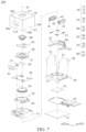
Please refer to FIG. 6 and FIG. 7 . FIG. 6 is a schematic view of an optical element driving mechanism 200 according to some embodiments of the present disclosure, wherein the outer frame is shown as a dashed line. FIG. 7 is an exploded view of the optical element driving mechanism 200 according to some embodiments of the present disclosure.
The main elements and the configuration of the optical element driving mechanism 200 is similar to that of optical element driving mechanism 100, and the similar parts will not be repeated.
As shown in FIG. 6 and FIG. 7 , the main difference between the optical element driving mechanism 200 and the optical element driving mechanism 100 is that the first support member 51 of the optical element driving mechanism 200 is not spherical, and the optical element driving mechanism 200 may not have second supporting element 52.
According to some embodiments of the present disclosure, the first supporting element 51 of the supporting assembly 50 of the optical element driving mechanism 200 may be a lifting wire. The first supporting element 51 may be connected to the first elastic element 56 of the elastic assembly 55, and the first supporting element 51 may be connected to the third optical element holder 31.
In addition, according to some embodiments of the present disclosure, the supporting assembly 50 of the optical element driving mechanism 200 may no longer have the second supporting element 52. Furthermore, the frame 13 is not in direct contact with the third optical element holder 31, and the bottom plate 12 is not in direct contact with the third optical element holder 31 either.
In this way, the third optical element holder 31 may move relative to the bottom plate 12 and the frame 13 along the first axis AX1 and/or the second axis AX2, so that the position of the third optical element 75 may be adjusted to improve the imaging quality.
In general, the optical element driving mechanism of some embodiments of the present disclosure may adjust the position of the optical element along the optical axis and the directions that are perpendicular to the optical axis, and the amount of incident light that incident to the optical element driving mechanism may be adjusted to improve the imaging quality of the optical element driving mechanism. Moreover, the optical element driving mechanism of some embodiments of the present disclosure may also be helpful for the optical element driving mechanism to be electrically connected to the outside, and the effect of miniaturization may also be achieved.
Although embodiments of the present disclosure and their advantages have been described in detail, it should be understood that various changes, substitutions and alterations may be made herein without departing from the spirit and scope of the disclosure as defined by the appended claims. For example, it will be readily understood by those skilled in the art that many of the features, functions, processes, and materials described herein may be varied while remaining within the scope of the present disclosure. Moreover, the scope of the present application is not intended to be limited to the particular embodiments of the process, machine, manufacture, composition of matter, means, methods and steps described in the specification. As one of ordinary skill in the art will readily appreciate from the disclosure of the present disclosure, processes, machines, manufacture, compositions of matter, means, methods, or steps, presently existing or later to be developed, that perform substantially the same function or achieve substantially the same result as the corresponding embodiments described herein may be utilized according to the present disclosure. Accordingly, the appended claims are intended to include within their scope such processes, machines, manufacture, compositions of matter, means, methods, or steps. In addition, the scope of the present disclosure is defined by the scope of the appended claims. In addition, each scope of the claims is constructed as a separate embodiment, and various combinations of the claims and combinations of embodiments are within the scope of the present disclosure.

Claims (19)

What is claimed is:
1. An optical element driving mechanism, comprising:
a first movable part, connected to a first optical element;
a second movable part, connected to a second optical element comprising an optical axis; and
a third movable part, connected to a third optical element;
wherein the first optical element, the second optical element, and the third optical element are arranged along the optical axis,
wherein the second optical element is located between the first optical element and the third optical element when viewed along a direction that is perpendicular to the optical axis,
wherein the second optical element has a second optical element top side and a second optical element bottom side opposite to the second optical element top side,
wherein the second optical element top side faces the first optical element,
wherein the area of the second optical element top side is smaller than the area of the second optical element bottom side.
2. The optical element driving mechanism as claimed in claim 1, further comprising a fixed part, connected to a fourth optical element,
wherein the first optical element, the second optical element, the third optical element, and the fourth optical element are arranged along the optical axis,
wherein the first optical element is located between the second optical element and the fourth optical element when viewed along the direction that is perpendicular to the optical axis,
wherein the first movable part comprises a first movable part limiting element, and the second movable part comprises a second movable part limiting element,
wherein the shortest distance between the first movable part limiting element and the second movable part limiting element is shorter than the shortest distance between the first optical element and the second optical element when viewed along the direction that is perpendicular to the optical axis.
3. The optical element driving mechanism as claimed in claim 2, wherein the first optical element is not in contact with the second optical element when the first movable part limiting element is in contact with the second movable part limiting element.
4. The optical element driving mechanism as claimed in claim 2, wherein the fourth optical element has a fourth optical element top side and a fourth optical element bottom side opposite to the fourth optical element top side,
wherein the fourth optical element bottom side faces the first optical element,
wherein the area of the fourth optical element top side is larger than the area of the fourth optical element bottom side.
5. The optical element driving mechanism as claimed in claim 2, wherein the first optical element is in active alignment with the second optical element, the second optical element is in active alignment with the third optical element, and the fourth optical element is in active alignment with the second optical element.
6. The optical element driving mechanism as claimed in claim 2, further comprising:
a first driving assembly, driving the first optical element to control the amount of the incident light; and
a second driving assembly, driving the second movable part to move relative to the fixed part,
wherein the fixed part has a polygonal structure when viewed along a direction that is parallel to the optical axis,
wherein the first driving assembly and the second driving assembly are located at different sides of the fixed part.
7. The optical element driving mechanism as claimed in claim 6, wherein the first driving assembly comprises a first driving magnetic element, and the second driving assembly comprises a second driving magnetic element,
wherein the fixed part comprises a first side, a second side, and a fourth side,
wherein the second side is parallel to the fourth side, and the first side is not parallel to the second side,
wherein the first driving magnetic element is disposed on the first side, and the second driving magnetic element is disposed on the second side and the fourth side.
8. The optical element driving mechanism as claimed in claim 6, further comprising:
a third driving assembly, driving the third movable part to move relative to the fixed part,
wherein the first driving assembly and the third driving assembly are located on different sides of the fixed part.
9. The optical element driving mechanism as claimed in claim 1, further comprising a fixed part, wherein the fixed part comprises an outer frame, and the outer frame comprises an outer frame top surface opening,
wherein a fourth optical element top side of the fourth optical element is exposed to the outer frame top surface opening.
10. An optical element driving mechanism, comprising:
a first movable part, connected to a first optical element;
a second movable part, connected to a second optical element comprising an optical axis; and
a third movable part, connected to a third optical element;
wherein the first optical element, the second optical element, and the third optical element are arranged along the optical axis,
wherein the second optical element is located between the first optical element and the third optical element when viewed along a direction that is perpendicular to the optical axis,
wherein the optical element driving mechanism further comprises a fixed part, wherein the fixed part comprises a frame, and the movable part comprises a third optical element holder,
wherein the frame accommodates the second movable part, and the third optical element holder accommodates the third optical element.
11. The optical element driving mechanism as claimed in claim 10, further comprising a first supporting element,
wherein the first supporting element is located between the frame and the third optical element holder,
wherein the frame is not in direct contact with the third optical element holder.
12. The optical element driving mechanism as claimed in claim 11, wherein the first supporting element is movable along a first axis that is perpendicular to the optical axis.
13. The optical element driving mechanism as claimed in claim 11, wherein the fixed part further comprises a bottom plate,
wherein the third optical element holder is located between the frame and the bottom plate,
wherein the third optical element holder is not in direct contact with the bottom plate.
14. The optical element driving mechanism as claimed in claim 13, wherein the first supporting element is movable along a first axis that is perpendicular to the optical axis and a second axis that is perpendicular to the optical axis and the first axis.
15. The optical element driving mechanism as claimed in claim 13, further comprising a second supporting element,
wherein the second supporting element is located between the third optical element holder and the bottom plate.
16. The optical element driving mechanism as claimed in claim 15, wherein the second supporting element is movable along a first axis that is perpendicular to the optical axis and a second axis that is perpendicular to the optical axis and the first axis.
17. The optical element driving mechanism as claimed in claim 10, further comprising a first supporting element and an elastic assembly,
wherein the frame is in contact with the elastic assembly,
wherein the first supporting element is connected to the elastic assembly, and the first supporting element is connected to the third optical element holder,
wherein the frame is not in direct contact with the third optical element holder.
18. An optical element driving mechanism, comprising:
a first movable part, connected to a first optical element;
a second movable part, connected to a second optical element comprising an optical axis; and
a third movable part, connected to a third optical element;
wherein the first optical element, the second optical element, and the third optical element are arranged along the optical axis,
wherein the second optical element is located between the first optical element and the third optical element when viewed along a direction that is perpendicular to the optical axis,
wherein the optical element driving mechanism further comprises a fixed part, wherein the fixed part comprises an outer frame, and the outer frame comprises an outer frame sidewall opening,
wherein a first circuit element that controls the first movable part is exposed to the outer frame sidewall opening.
19. An optical element driving mechanism, comprising:
a first movable part, connected to a first optical element;
a second movable part, connected to a second optical element comprising an optical axis; and
a third movable part, connected to a third optical element;
wherein the first optical element, the second optical element, and the third optical element are arranged along the optical axis,
wherein the second optical element is located between the first optical element and the third optical element when viewed along a direction that is perpendicular to the optical axis,
wherein the optical element driving mechanism further comprises a fixed part, wherein the fixed part comprises an outer frame, and the outer frame comprises an outer frame sidewall recess,
wherein a third circuit element that controls the third optical element is exposed to the outer frame sidewall recess.
US17/553,126 2020-12-18 2021-12-16 Optical element driving mechanism Active 2044-02-09 US12356071B2 (en)

Priority Applications (2)

Application Number Priority Date Filing Date Title
US17/553,126 US12356071B2 (en) 2020-12-18 2021-12-16 Optical element driving mechanism
US19/237,320 US20250310645A1 (en) 2020-12-18 2025-06-13 Optical element driving mechanism

Applications Claiming Priority (2)

Application Number Priority Date Filing Date Title
US202063127746P 2020-12-18 2020-12-18
US17/553,126 US12356071B2 (en) 2020-12-18 2021-12-16 Optical element driving mechanism

Related Child Applications (1)

Application Number Title Priority Date Filing Date
US19/237,320 Continuation US20250310645A1 (en) 2020-12-18 2025-06-13 Optical element driving mechanism

Publications (2)

Publication Number Publication Date
US20220196974A1 US20220196974A1 (en) 2022-06-23
US12356071B2 true US12356071B2 (en) 2025-07-08

Family

ID=81884628

Family Applications (9)

Application Number Title Priority Date Filing Date
US17/552,422 Active US11835683B2 (en) 2020-12-18 2021-12-16 Tactile feedback mechanism
US17/553,069 Active 2044-01-12 US12323704B2 (en) 2020-12-18 2021-12-16 Optical element driving mechanism
US17/553,126 Active 2044-02-09 US12356071B2 (en) 2020-12-18 2021-12-16 Optical element driving mechanism
US17/554,290 Active 2043-12-25 US12368956B2 (en) 2020-12-18 2021-12-17 Optical system
US17/554,385 Active 2043-11-02 US12452533B2 (en) 2020-12-18 2021-12-17 Optical component driving mechanism
US17/554,644 Active 2043-04-11 US12181631B2 (en) 2020-12-18 2021-12-17 Optical element driving mechanism
US17/556,090 Active 2043-12-25 US12375809B2 (en) 2020-12-18 2021-12-20 Driving mechanism
US19/197,142 Pending US20250274660A1 (en) 2020-12-18 2025-05-02 Optical element driving mechanism
US19/237,320 Pending US20250310645A1 (en) 2020-12-18 2025-06-13 Optical element driving mechanism

Family Applications Before (2)

Application Number Title Priority Date Filing Date
US17/552,422 Active US11835683B2 (en) 2020-12-18 2021-12-16 Tactile feedback mechanism
US17/553,069 Active 2044-01-12 US12323704B2 (en) 2020-12-18 2021-12-16 Optical element driving mechanism

Family Applications After (6)

Application Number Title Priority Date Filing Date
US17/554,290 Active 2043-12-25 US12368956B2 (en) 2020-12-18 2021-12-17 Optical system
US17/554,385 Active 2043-11-02 US12452533B2 (en) 2020-12-18 2021-12-17 Optical component driving mechanism
US17/554,644 Active 2043-04-11 US12181631B2 (en) 2020-12-18 2021-12-17 Optical element driving mechanism
US17/556,090 Active 2043-12-25 US12375809B2 (en) 2020-12-18 2021-12-20 Driving mechanism
US19/197,142 Pending US20250274660A1 (en) 2020-12-18 2025-05-02 Optical element driving mechanism
US19/237,320 Pending US20250310645A1 (en) 2020-12-18 2025-06-13 Optical element driving mechanism

Country Status (2)

Country Link
US (9) US11835683B2 (en)
CN (12) CN114721104A (en)

Families Citing this family (8)

* Cited by examiner, † Cited by third party
Publication number Priority date Publication date Assignee Title
CN115145019B (en) * 2018-01-25 2023-12-08 台湾东电化股份有限公司 Optical system
EP4249969A3 (en) 2018-12-27 2024-01-10 Tdk Taiwan Corp. Optical member driving mechanism
CN213423564U (en) * 2020-02-10 2021-06-11 台湾东电化股份有限公司 Optical element drive mechanism
US11835683B2 (en) * 2020-12-18 2023-12-05 Tdk Taiwan Corp. Tactile feedback mechanism
CN218446243U (en) * 2021-10-22 2023-02-03 台湾东电化股份有限公司 Optical system
US20230209201A1 (en) * 2021-12-27 2023-06-29 Tdk Taiwan Corp. Method for controlling optical element driving mechanism
CN220913408U (en) 2022-07-13 2024-05-07 台湾东电化股份有限公司 Optical element drive mechanism
CN221926877U (en) * 2022-11-28 2024-10-29 台湾东电化股份有限公司 Optical system

Citations (4)

* Cited by examiner, † Cited by third party
Publication number Priority date Publication date Assignee Title
US20200142161A1 (en) * 2018-11-05 2020-05-07 Samsung Electro-Mechanics Co., Ltd. Lens module, camera module, and portable electronic device
US20210063680A1 (en) * 2018-01-31 2021-03-04 Lg Innotek Co., Ltd. Camera module
US20230042087A1 (en) * 2020-11-10 2023-02-09 Beijing Xiaomi Mobile Software Co., Ltd. Optical imaging system, method for performing optical image stabilization
US20240159987A1 (en) * 2022-11-14 2024-05-16 Canon Kabushiki Kaisha Optical device and image pickup apparatus

Family Cites Families (97)

* Cited by examiner, † Cited by third party
Publication number Priority date Publication date Assignee Title
US260076A (en) * 1882-06-27 Folding camera
US4628907A (en) * 1984-03-22 1986-12-16 Epley John M Direct contact hearing aid apparatus
US7025513B2 (en) * 2002-11-18 2006-04-11 Olympus Corporation Optical apparatus, shutter device, and camera
JP2004274242A (en) * 2003-03-06 2004-09-30 Minolta Co Ltd Digital camera
JP2007078907A (en) * 2005-09-13 2007-03-29 Seiko Instruments Inc Lens drive module and camera module
GB0606425D0 (en) * 2006-03-30 2006-05-10 1 Ltd Camera lens actuation apparatus
TWM325524U (en) * 2007-03-20 2008-01-11 Tricore Corp Improvement of driving and positing assignment for focusing actuator
JP2008253077A (en) * 2007-03-30 2008-10-16 Nikon Corp Vibration actuator, lens barrel and camera
TWI347725B (en) * 2007-04-09 2011-08-21 Voice coil motor apparatus for positioning
WO2009004975A1 (en) * 2007-06-29 2009-01-08 Nidec Copal Corporation Camera blade driving device
CN101378218B (en) * 2007-08-31 2010-09-15 财团法人工业技术研究院 electromagnetic transmission device
DE602008006763D1 (en) * 2007-10-30 2011-06-16 Cambridge Mechatronics Ltd MEMORY ALLOY ACTUATOR
JP4958804B2 (en) * 2008-01-22 2012-06-20 キヤノン株式会社 Optical lens barrel and imaging device
TW201007245A (en) * 2008-08-07 2010-02-16 Ind Tech Res Inst Voice coil motor and optical device
JP5284008B2 (en) * 2008-08-26 2013-09-11 キヤノン株式会社 Observation device
JP5369725B2 (en) * 2009-01-30 2013-12-18 株式会社ニコン Imaging device
JP5232048B2 (en) * 2009-03-12 2013-07-10 株式会社シグマ Optical correction unit assembling method, optical correction unit, lens barrel having optical correction unit, and imaging apparatus
JP4820460B2 (en) * 2009-10-22 2011-11-24 パナソニック株式会社 Focus system, interchangeable lens and imaging device
JP5079049B2 (en) * 2009-11-17 2012-11-21 台湾東電化股▲ふん▼有限公司 Lens drive device
KR101409662B1 (en) * 2010-01-29 2014-06-18 니혼도꾸슈도교 가부시키가이샤 Lead-free piezoelectric ceramic composition, piezoelectric element comprising same, knock sensor, and process for production of lead-free piezoelectric ceramic composition
JP5622443B2 (en) * 2010-06-08 2014-11-12 日本電産サンキョー株式会社 Optical unit with shake correction function
US8963695B2 (en) * 2011-05-27 2015-02-24 Apple Inc. Haptic alert device having a linear vibrator
WO2013008418A1 (en) * 2011-07-13 2013-01-17 日本特殊陶業株式会社 Lead-free piezoelectric ceramic composition, method for producing same, piezoelectric element using lead-free piezoelectric ceramic composition, ultrasonic processing machine, ultrasonic drive device, and sensing device
JP5821356B2 (en) * 2011-07-15 2015-11-24 ミツミ電機株式会社 Lens drive device
CN102890385B (en) * 2011-07-18 2016-08-31 鸿富锦精密工业(深圳)有限公司 Actuator and there is the camera module of this actuator
JP5787716B2 (en) * 2011-10-24 2015-09-30 キヤノン株式会社 Zoom lens and imaging apparatus having the same
JP2013114167A (en) * 2011-11-30 2013-06-10 Jvc Kenwood Corp Imaging apparatus
JP2013238848A (en) * 2012-04-20 2013-11-28 Hoya Corp Imaging apparatus
KR101932795B1 (en) * 2012-05-25 2018-12-26 캠브리지 메카트로닉스 리미티드 Shape memory alloy actuation apparatus
TW201415970A (en) * 2012-08-10 2014-04-16 Digitaloptics Corp Auto-focus camera module with flexible printed circuit extension
JP6114050B2 (en) * 2013-02-04 2017-04-12 Hoya株式会社 Imaging device
JP6114049B2 (en) * 2013-02-04 2017-04-12 Hoya株式会社 Imaging device
CN203775401U (en) * 2013-07-09 2014-08-13 瑞声科技(南京)有限公司 Piezoelectric device
KR102125558B1 (en) * 2013-08-19 2020-06-22 삼성전자주식회사 Camera module, position detector and position detection method
JP6143622B2 (en) * 2013-09-25 2017-06-07 日本電産サンキョー株式会社 Optical unit with shake correction function
JP6237106B2 (en) * 2013-10-18 2017-11-29 コニカミノルタ株式会社 Zoom lens and imaging device
US9618770B2 (en) * 2014-04-11 2017-04-11 Samsung Electro-Mechanics Co., Ltd. Camera module with function of auto-focus and image stabilize
CN204129301U (en) * 2014-09-29 2015-01-28 浙江水晶光电科技股份有限公司 Optical lens electro-optical device
US9366879B1 (en) * 2014-12-02 2016-06-14 Hutchinson Technology Incorporated Camera lens suspension with polymer bearings
US10830982B2 (en) * 2014-12-24 2020-11-10 Ultimems, Inc. Autofocus system
JP2017003931A (en) * 2015-06-16 2017-01-05 リコーイメージング株式会社 Drive unit
TW201705745A (en) * 2015-07-17 2017-02-01 愛瑪麗歐股份有限公司 Camera base device with screw-in plug
JP6708920B2 (en) * 2015-11-16 2020-06-10 ミツミ電機株式会社 Lens driving device, camera module, and camera mounting device
TWI636313B (en) * 2016-05-10 2018-09-21 台灣東電化股份有限公司 Lens system
JP6853487B2 (en) * 2016-05-31 2021-03-31 ミツミ電機株式会社 Lens drive, camera module, and camera mount
TWI616675B (en) * 2016-07-14 2018-03-01 大立光電股份有限公司 Optical photographing assembly, image capturing apparatus and electronic device
EP3490242B1 (en) * 2016-07-21 2022-10-12 LG Innotek Co., Ltd. Lens driving device, and camera module
KR102767487B1 (en) * 2016-12-08 2025-02-14 삼성전자주식회사 Camera Module including a aperture and Electronic device including the same
CN115201993B (en) * 2017-01-09 2024-06-07 Lg伊诺特有限公司 Camera module, optical device, and lens driving device
KR102675551B1 (en) * 2017-01-09 2024-06-17 엘지이노텍 주식회사 Dual lens driving device, dual camera module and optical apparatus
CN113805405B (en) * 2017-01-12 2023-05-23 核心光电有限公司 Compact folding camera and method of assembling the same
CN110574297B (en) * 2017-02-16 2022-01-11 沃特洛电气制造公司 Compact modular wireless sensor
US11381147B2 (en) * 2017-02-16 2022-07-05 Tdk Taiwan Corp. Driving mechanism
CN113848626B (en) * 2017-05-17 2023-08-15 台湾东电化股份有限公司 Drive mechanism
KR102029532B1 (en) * 2017-06-12 2019-10-07 삼성전기주식회사 Lens driving apparatus and camera module including the same
CN207069859U (en) * 2017-06-12 2018-03-02 歌尔股份有限公司 Electromagnetic driver and electronic equipment
US10809487B2 (en) * 2017-06-13 2020-10-20 Tdk Taiwan Corp. Optical system
CN109089020B (en) * 2017-06-13 2021-06-04 台湾东电化股份有限公司 Optical system
JPWO2019017286A1 (en) * 2017-07-18 2020-07-30 パナソニックIpマネジメント株式会社 Actuator and camera device
CN109391750B (en) * 2017-08-05 2023-05-12 宁波舜宇光电信息有限公司 Fixed focus camera module
KR102485461B1 (en) * 2017-08-07 2023-01-06 엘지이노텍 주식회사 Lens driving device, camera module and optical apparatus
US10895642B2 (en) * 2017-10-18 2021-01-19 Tdk Taiwan Corp. Distance measuring device
CN207623606U (en) * 2017-10-25 2018-07-17 瑞声科技(新加坡)有限公司 Lens assembly
KR102104453B1 (en) * 2017-11-09 2020-05-29 삼성전기주식회사 Camera module
US11190085B2 (en) * 2017-12-07 2021-11-30 Tdk Taiwan Corp. Multi-lens camera system and driving mechanism thereof
CN111566557B (en) * 2017-12-19 2022-07-29 Lg伊诺特有限公司 Lens driving device and camera module
CN115145019B (en) * 2018-01-25 2023-12-08 台湾东电化股份有限公司 Optical system
US10928702B2 (en) * 2018-03-20 2021-02-23 Samsung Electro-Mechanics Co., Ltd. Portable electronic apparatus and camera module
CN108710189B (en) * 2018-07-04 2024-08-16 上海比路电子股份有限公司 Lens driving motor, camera and mobile terminal device
US11396928B2 (en) * 2018-07-15 2022-07-26 Delbert Tesar Actuator with a parallel eccentric gear train driven by a mechanically amplified piezoelectric assembly
CN209803439U (en) * 2018-07-25 2019-12-17 台湾东电化股份有限公司 Drive mechanism
CN110784625B (en) * 2018-07-25 2022-04-15 台湾东电化股份有限公司 Driving mechanism of photosensitive assembly
US20200033558A1 (en) * 2018-07-25 2020-01-30 Tdk Taiwan Corp. Optical element driving system and mechanism thereof
CN212255842U (en) * 2018-08-24 2020-12-29 台湾东电化股份有限公司 Optical assembly driving mechanism
KR102635884B1 (en) * 2018-10-31 2024-02-14 삼성전자주식회사 A camera module including an aperture
KR102278971B1 (en) * 2018-11-14 2021-07-20 아사히 가세이 일렉트로닉스 가부시끼가이샤 Camera module
US11601595B2 (en) * 2019-02-01 2023-03-07 Tdk Taiwan Corp. Control method of driving mechanism
US11340418B2 (en) * 2018-12-27 2022-05-24 Tdk Taiwan Corp. Optical member driving mechanism
EP4130836A3 (en) * 2018-12-27 2023-05-24 Tdk Taiwan Corp. Optical system
EP4249969A3 (en) * 2018-12-27 2024-01-10 Tdk Taiwan Corp. Optical member driving mechanism
US11693208B2 (en) * 2019-02-01 2023-07-04 Tdk Taiwan Corp. Optical sensing system
EP3699664B8 (en) * 2019-02-01 2025-05-14 Tdk Taiwan Corp. Optical element driving mechanism
US11506862B2 (en) * 2019-02-01 2022-11-22 Tdk Taiwan Corp. Optical element driving mechanism
KR102849668B1 (en) * 2019-03-28 2025-08-22 엘지이노텍 주식회사 Camera module
CN111835967B (en) * 2019-04-19 2023-08-18 台湾东电化股份有限公司 Photosensitive component drive mechanism
CN211718601U (en) * 2019-05-17 2020-10-20 台湾东电化股份有限公司 Optical element driving mechanism
CN211741661U (en) * 2019-06-14 2020-10-23 台湾东电化股份有限公司 Optical element drive mechanism
CN211826653U (en) * 2019-07-26 2020-10-30 台湾东电化股份有限公司 Optical element drive mechanism and optical system
CN211878277U (en) 2019-09-12 2020-11-06 台湾东电化股份有限公司 Optical element drive mechanism
US11425487B2 (en) * 2019-11-29 2022-08-23 Em-Tech Co., Ltd. Translation system using sound vibration microphone
CN113031194B (en) 2019-12-06 2025-05-13 台湾东电化股份有限公司 Optical element driving mechanism
US11947180B2 (en) * 2019-12-26 2024-04-02 Tdk Taiwan Corp. Optical system
KR102894850B1 (en) * 2019-12-27 2025-12-03 삼성전기주식회사 Position detection apparatus of aperture module
EP4187894A4 (en) * 2020-07-21 2024-08-07 LG Innotek Co., Ltd. CAMERA ACTUATOR AND CAMERA MODULE
TWI738514B (en) * 2020-09-16 2021-09-01 大陽科技股份有限公司 Camera module using reflecting element and electronic device
CN112255818B (en) * 2020-11-03 2022-06-03 广州立景创新科技有限公司 Imaging correction unit and imaging module
US11835683B2 (en) * 2020-12-18 2023-12-05 Tdk Taiwan Corp. Tactile feedback mechanism

Patent Citations (4)

* Cited by examiner, † Cited by third party
Publication number Priority date Publication date Assignee Title
US20210063680A1 (en) * 2018-01-31 2021-03-04 Lg Innotek Co., Ltd. Camera module
US20200142161A1 (en) * 2018-11-05 2020-05-07 Samsung Electro-Mechanics Co., Ltd. Lens module, camera module, and portable electronic device
US20230042087A1 (en) * 2020-11-10 2023-02-09 Beijing Xiaomi Mobile Software Co., Ltd. Optical imaging system, method for performing optical image stabilization
US20240159987A1 (en) * 2022-11-14 2024-05-16 Canon Kabushiki Kaisha Optical device and image pickup apparatus

Also Published As

Publication number Publication date
CN216718781U (en) 2022-06-10
US12323704B2 (en) 2025-06-03
CN216718787U (en) 2022-06-10
US20250274660A1 (en) 2025-08-28
CN114721115A (en) 2022-07-08
US12368956B2 (en) 2025-07-22
US12452533B2 (en) 2025-10-21
US20220196966A1 (en) 2022-06-23
US20220197010A1 (en) 2022-06-23
US12375809B2 (en) 2025-07-29
US20250310645A1 (en) 2025-10-02
US12181631B2 (en) 2024-12-31
US20220196965A1 (en) 2022-06-23
CN216718780U (en) 2022-06-10
CN114721104A (en) 2022-07-08
CN114647307A (en) 2022-06-21
US20220196974A1 (en) 2022-06-23
CN216718788U (en) 2022-06-10
CN114721116A (en) 2022-07-08
CN114721116B (en) 2026-01-09
US20220197386A1 (en) 2022-06-23
US20220197050A1 (en) 2022-06-23
CN114721119A (en) 2022-07-08
US20220197046A1 (en) 2022-06-23
CN114721117A (en) 2022-07-08
US11835683B2 (en) 2023-12-05
CN114721105A (en) 2022-07-08
CN114647307B (en) 2025-10-21
CN217606160U (en) 2022-10-18

Similar Documents

Publication Publication Date Title
US12356071B2 (en) Optical element driving mechanism
US11604327B2 (en) Optical element driving mechanism
US11314102B2 (en) Lens driving device
US11187965B2 (en) Optical element driving mechanism with stopping assembly
US11126068B2 (en) Optical system
US12326654B2 (en) Optical element driving mechanism
US20220269034A1 (en) Optical element driving mechanism
US12289510B2 (en) Optical element driving mechanism with supporting assembly
US11681156B2 (en) Optical element driving mechanism
US12235572B2 (en) Optical element driving mechanism
US20230127990A1 (en) Optical element driving mechanism
US20250028150A1 (en) Optical element driving mechanism
TWI695217B (en) Imaging lens module and electronic device
US11561410B2 (en) Driving mechanism for optical element
US20250116844A1 (en) Optical system
US20240085718A1 (en) Optical element driving mechanism
US12235571B2 (en) Optical element driving mechanism
US11630280B2 (en) Optical element driving mechanism
US20240369909A1 (en) Optical module
US20240019760A1 (en) Optical element driving mechanism
US20240152035A1 (en) Optical system
US20250164739A1 (en) Optical element driving mechanism
WO2022087786A1 (en) Periscopic camera module and electronic device

Legal Events

Date Code Title Description
FEPP Fee payment procedure

Free format text: ENTITY STATUS SET TO UNDISCOUNTED (ORIGINAL EVENT CODE: BIG.); ENTITY STATUS OF PATENT OWNER: LARGE ENTITY

AS Assignment

Owner name: TDK TAIWAN CORP., TAIWAN

Free format text: ASSIGNMENT OF ASSIGNORS INTEREST;ASSIGNORS:CHEN, SHU-SHAN;HU, CHAO-CHANG;WENG, CHIH-WEI;REEL/FRAME:058623/0805

Effective date: 20211207

STPP Information on status: patent application and granting procedure in general

Free format text: DOCKETED NEW CASE - READY FOR EXAMINATION

STPP Information on status: patent application and granting procedure in general

Free format text: NON FINAL ACTION MAILED

STPP Information on status: patent application and granting procedure in general

Free format text: RESPONSE TO NON-FINAL OFFICE ACTION ENTERED AND FORWARDED TO EXAMINER

STPP Information on status: patent application and granting procedure in general

Free format text: NOTICE OF ALLOWANCE MAILED -- APPLICATION RECEIVED IN OFFICE OF PUBLICATIONS

STCF Information on status: patent grant

Free format text: PATENTED CASE