US12355019B2 - Display apparatus and electronic device - Google Patents
Display apparatus and electronic device Download PDFInfo
- Publication number
- US12355019B2 US12355019B2 US18/026,634 US202118026634A US12355019B2 US 12355019 B2 US12355019 B2 US 12355019B2 US 202118026634 A US202118026634 A US 202118026634A US 12355019 B2 US12355019 B2 US 12355019B2
- Authority
- US
- United States
- Prior art keywords
- transistor
- electrode
- light
- display apparatus
- layer
- Prior art date
- Legal status (The legal status is an assumption and is not a legal conclusion. Google has not performed a legal analysis and makes no representation as to the accuracy of the status listed.)
- Active
Links
Images


Classifications
-
- H01L25/167—
-
- G—PHYSICS
- G09—EDUCATION; CRYPTOGRAPHY; DISPLAY; ADVERTISING; SEALS
- G09G—ARRANGEMENTS OR CIRCUITS FOR CONTROL OF INDICATING DEVICES USING STATIC MEANS TO PRESENT VARIABLE INFORMATION
- G09G3/00—Control arrangements or circuits, of interest only in connection with visual indicators other than cathode-ray tubes
- G09G3/20—Control arrangements or circuits, of interest only in connection with visual indicators other than cathode-ray tubes for presentation of an assembly of a number of characters, e.g. a page, by composing the assembly by combination of individual elements arranged in a matrix no fixed position being assigned to or needed to be assigned to the individual characters or partial characters
- G09G3/22—Control arrangements or circuits, of interest only in connection with visual indicators other than cathode-ray tubes for presentation of an assembly of a number of characters, e.g. a page, by composing the assembly by combination of individual elements arranged in a matrix no fixed position being assigned to or needed to be assigned to the individual characters or partial characters using controlled light sources
- G09G3/30—Control arrangements or circuits, of interest only in connection with visual indicators other than cathode-ray tubes for presentation of an assembly of a number of characters, e.g. a page, by composing the assembly by combination of individual elements arranged in a matrix no fixed position being assigned to or needed to be assigned to the individual characters or partial characters using controlled light sources using electroluminescent panels
- G09G3/32—Control arrangements or circuits, of interest only in connection with visual indicators other than cathode-ray tubes for presentation of an assembly of a number of characters, e.g. a page, by composing the assembly by combination of individual elements arranged in a matrix no fixed position being assigned to or needed to be assigned to the individual characters or partial characters using controlled light sources using electroluminescent panels semiconductive, e.g. using light-emitting diodes [LED]
- G09G3/3208—Control arrangements or circuits, of interest only in connection with visual indicators other than cathode-ray tubes for presentation of an assembly of a number of characters, e.g. a page, by composing the assembly by combination of individual elements arranged in a matrix no fixed position being assigned to or needed to be assigned to the individual characters or partial characters using controlled light sources using electroluminescent panels semiconductive, e.g. using light-emitting diodes [LED] organic, e.g. using organic light-emitting diodes [OLED]
- G09G3/3225—Control arrangements or circuits, of interest only in connection with visual indicators other than cathode-ray tubes for presentation of an assembly of a number of characters, e.g. a page, by composing the assembly by combination of individual elements arranged in a matrix no fixed position being assigned to or needed to be assigned to the individual characters or partial characters using controlled light sources using electroluminescent panels semiconductive, e.g. using light-emitting diodes [LED] organic, e.g. using organic light-emitting diodes [OLED] using an active matrix
- G09G3/3233—Control arrangements or circuits, of interest only in connection with visual indicators other than cathode-ray tubes for presentation of an assembly of a number of characters, e.g. a page, by composing the assembly by combination of individual elements arranged in a matrix no fixed position being assigned to or needed to be assigned to the individual characters or partial characters using controlled light sources using electroluminescent panels semiconductive, e.g. using light-emitting diodes [LED] organic, e.g. using organic light-emitting diodes [OLED] using an active matrix with pixel circuitry controlling the current through the light-emitting element
-
- G—PHYSICS
- G09—EDUCATION; CRYPTOGRAPHY; DISPLAY; ADVERTISING; SEALS
- G09F—DISPLAYING; ADVERTISING; SIGNS; LABELS OR NAME-PLATES; SEALS
- G09F9/00—Indicating arrangements for variable information in which the information is built-up on a support by selection or combination of individual elements
- G09F9/30—Indicating arrangements for variable information in which the information is built-up on a support by selection or combination of individual elements in which the desired character or characters are formed by combining individual elements
- G09F9/33—Indicating arrangements for variable information in which the information is built-up on a support by selection or combination of individual elements in which the desired character or characters are formed by combining individual elements being semiconductor devices, e.g. diodes
-
- G—PHYSICS
- G09—EDUCATION; CRYPTOGRAPHY; DISPLAY; ADVERTISING; SEALS
- G09G—ARRANGEMENTS OR CIRCUITS FOR CONTROL OF INDICATING DEVICES USING STATIC MEANS TO PRESENT VARIABLE INFORMATION
- G09G3/00—Control arrangements or circuits, of interest only in connection with visual indicators other than cathode-ray tubes
- G09G3/20—Control arrangements or circuits, of interest only in connection with visual indicators other than cathode-ray tubes for presentation of an assembly of a number of characters, e.g. a page, by composing the assembly by combination of individual elements arranged in a matrix no fixed position being assigned to or needed to be assigned to the individual characters or partial characters
- G09G3/22—Control arrangements or circuits, of interest only in connection with visual indicators other than cathode-ray tubes for presentation of an assembly of a number of characters, e.g. a page, by composing the assembly by combination of individual elements arranged in a matrix no fixed position being assigned to or needed to be assigned to the individual characters or partial characters using controlled light sources
- G09G3/30—Control arrangements or circuits, of interest only in connection with visual indicators other than cathode-ray tubes for presentation of an assembly of a number of characters, e.g. a page, by composing the assembly by combination of individual elements arranged in a matrix no fixed position being assigned to or needed to be assigned to the individual characters or partial characters using controlled light sources using electroluminescent panels
- G09G3/32—Control arrangements or circuits, of interest only in connection with visual indicators other than cathode-ray tubes for presentation of an assembly of a number of characters, e.g. a page, by composing the assembly by combination of individual elements arranged in a matrix no fixed position being assigned to or needed to be assigned to the individual characters or partial characters using controlled light sources using electroluminescent panels semiconductive, e.g. using light-emitting diodes [LED]
- G09G3/3208—Control arrangements or circuits, of interest only in connection with visual indicators other than cathode-ray tubes for presentation of an assembly of a number of characters, e.g. a page, by composing the assembly by combination of individual elements arranged in a matrix no fixed position being assigned to or needed to be assigned to the individual characters or partial characters using controlled light sources using electroluminescent panels semiconductive, e.g. using light-emitting diodes [LED] organic, e.g. using organic light-emitting diodes [OLED]
- G09G3/3225—Control arrangements or circuits, of interest only in connection with visual indicators other than cathode-ray tubes for presentation of an assembly of a number of characters, e.g. a page, by composing the assembly by combination of individual elements arranged in a matrix no fixed position being assigned to or needed to be assigned to the individual characters or partial characters using controlled light sources using electroluminescent panels semiconductive, e.g. using light-emitting diodes [LED] organic, e.g. using organic light-emitting diodes [OLED] using an active matrix
-
- H—ELECTRICITY
- H10—SEMICONDUCTOR DEVICES; ELECTRIC SOLID-STATE DEVICES NOT OTHERWISE PROVIDED FOR
- H10D—INORGANIC ELECTRIC SEMICONDUCTOR DEVICES
- H10D30/00—Field-effect transistors [FET]
- H10D30/60—Insulated-gate field-effect transistors [IGFET]
- H10D30/67—Thin-film transistors [TFT]
-
- H—ELECTRICITY
- H10—SEMICONDUCTOR DEVICES; ELECTRIC SOLID-STATE DEVICES NOT OTHERWISE PROVIDED FOR
- H10H—INORGANIC LIGHT-EMITTING SEMICONDUCTOR DEVICES HAVING POTENTIAL BARRIERS
- H10H20/00—Individual inorganic light-emitting semiconductor devices having potential barriers, e.g. light-emitting diodes [LED]
- H10H20/80—Constructional details
- H10H20/85—Packages
- H10H20/857—Interconnections, e.g. lead-frames, bond wires or solder balls
-
- H—ELECTRICITY
- H10—SEMICONDUCTOR DEVICES; ELECTRIC SOLID-STATE DEVICES NOT OTHERWISE PROVIDED FOR
- H10H—INORGANIC LIGHT-EMITTING SEMICONDUCTOR DEVICES HAVING POTENTIAL BARRIERS
- H10H29/00—Integrated devices, or assemblies of multiple devices, comprising at least one light-emitting semiconductor element covered by group H10H20/00
- H10H29/10—Integrated devices comprising at least one light-emitting semiconductor component covered by group H10H20/00
- H10H29/14—Integrated devices comprising at least one light-emitting semiconductor component covered by group H10H20/00 comprising multiple light-emitting semiconductor components
- H10H29/142—Two-dimensional arrangements, e.g. asymmetric LED layout
-
- H—ELECTRICITY
- H10—SEMICONDUCTOR DEVICES; ELECTRIC SOLID-STATE DEVICES NOT OTHERWISE PROVIDED FOR
- H10K—ORGANIC ELECTRIC SOLID-STATE DEVICES
- H10K59/00—Integrated devices, or assemblies of multiple devices, comprising at least one organic light-emitting element covered by group H10K50/00
- H10K59/10—OLED displays
- H10K59/12—Active-matrix OLED [AMOLED] displays
- H10K59/121—Active-matrix OLED [AMOLED] displays characterised by the geometry or disposition of pixel elements
- H10K59/1213—Active-matrix OLED [AMOLED] displays characterised by the geometry or disposition of pixel elements the pixel elements being TFTs
-
- H—ELECTRICITY
- H10—SEMICONDUCTOR DEVICES; ELECTRIC SOLID-STATE DEVICES NOT OTHERWISE PROVIDED FOR
- H10K—ORGANIC ELECTRIC SOLID-STATE DEVICES
- H10K59/00—Integrated devices, or assemblies of multiple devices, comprising at least one organic light-emitting element covered by group H10K50/00
- H10K59/10—OLED displays
- H10K59/12—Active-matrix OLED [AMOLED] displays
- H10K59/131—Interconnections, e.g. wiring lines or terminals
-
- H—ELECTRICITY
- H10—SEMICONDUCTOR DEVICES; ELECTRIC SOLID-STATE DEVICES NOT OTHERWISE PROVIDED FOR
- H10W—GENERIC PACKAGES, INTERCONNECTIONS, CONNECTORS OR OTHER CONSTRUCTIONAL DETAILS OF DEVICES COVERED BY CLASS H10
- H10W90/00—Package configurations
-
- G—PHYSICS
- G09—EDUCATION; CRYPTOGRAPHY; DISPLAY; ADVERTISING; SEALS
- G09G—ARRANGEMENTS OR CIRCUITS FOR CONTROL OF INDICATING DEVICES USING STATIC MEANS TO PRESENT VARIABLE INFORMATION
- G09G2300/00—Aspects of the constitution of display devices
- G09G2300/04—Structural and physical details of display devices
- G09G2300/0421—Structural details of the set of electrodes
- G09G2300/0426—Layout of electrodes and connections
-
- G—PHYSICS
- G09—EDUCATION; CRYPTOGRAPHY; DISPLAY; ADVERTISING; SEALS
- G09G—ARRANGEMENTS OR CIRCUITS FOR CONTROL OF INDICATING DEVICES USING STATIC MEANS TO PRESENT VARIABLE INFORMATION
- G09G2300/00—Aspects of the constitution of display devices
- G09G2300/08—Active matrix structure, i.e. with use of active elements, inclusive of non-linear two terminal elements, in the pixels together with light emitting or modulating elements
- G09G2300/0809—Several active elements per pixel in active matrix panels
- G09G2300/0819—Several active elements per pixel in active matrix panels used for counteracting undesired variations, e.g. feedback or autozeroing
-
- G—PHYSICS
- G09—EDUCATION; CRYPTOGRAPHY; DISPLAY; ADVERTISING; SEALS
- G09G—ARRANGEMENTS OR CIRCUITS FOR CONTROL OF INDICATING DEVICES USING STATIC MEANS TO PRESENT VARIABLE INFORMATION
- G09G2300/00—Aspects of the constitution of display devices
- G09G2300/08—Active matrix structure, i.e. with use of active elements, inclusive of non-linear two terminal elements, in the pixels together with light emitting or modulating elements
- G09G2300/0809—Several active elements per pixel in active matrix panels
- G09G2300/0842—Several active elements per pixel in active matrix panels forming a memory circuit, e.g. a dynamic memory with one capacitor
- G09G2300/0861—Several active elements per pixel in active matrix panels forming a memory circuit, e.g. a dynamic memory with one capacitor with additional control of the display period without amending the charge stored in a pixel memory, e.g. by means of additional select electrodes
-
- G—PHYSICS
- G09—EDUCATION; CRYPTOGRAPHY; DISPLAY; ADVERTISING; SEALS
- G09G—ARRANGEMENTS OR CIRCUITS FOR CONTROL OF INDICATING DEVICES USING STATIC MEANS TO PRESENT VARIABLE INFORMATION
- G09G2310/00—Command of the display device
- G09G2310/06—Details of flat display driving waveforms
- G09G2310/066—Waveforms comprising a gently increasing or decreasing portion, e.g. ramp
-
- G—PHYSICS
- G09—EDUCATION; CRYPTOGRAPHY; DISPLAY; ADVERTISING; SEALS
- G09G—ARRANGEMENTS OR CIRCUITS FOR CONTROL OF INDICATING DEVICES USING STATIC MEANS TO PRESENT VARIABLE INFORMATION
- G09G2310/00—Command of the display device
- G09G2310/08—Details of timing specific for flat panels, other than clock recovery
-
- G—PHYSICS
- G09—EDUCATION; CRYPTOGRAPHY; DISPLAY; ADVERTISING; SEALS
- G09G—ARRANGEMENTS OR CIRCUITS FOR CONTROL OF INDICATING DEVICES USING STATIC MEANS TO PRESENT VARIABLE INFORMATION
- G09G2320/00—Control of display operating conditions
- G09G2320/02—Improving the quality of display appearance
-
- G—PHYSICS
- G09—EDUCATION; CRYPTOGRAPHY; DISPLAY; ADVERTISING; SEALS
- G09G—ARRANGEMENTS OR CIRCUITS FOR CONTROL OF INDICATING DEVICES USING STATIC MEANS TO PRESENT VARIABLE INFORMATION
- G09G2320/00—Control of display operating conditions
- G09G2320/06—Adjustment of display parameters
- G09G2320/0626—Adjustment of display parameters for control of overall brightness
- G09G2320/064—Adjustment of display parameters for control of overall brightness by time modulation of the brightness of the illumination source
-
- G—PHYSICS
- G09—EDUCATION; CRYPTOGRAPHY; DISPLAY; ADVERTISING; SEALS
- G09G—ARRANGEMENTS OR CIRCUITS FOR CONTROL OF INDICATING DEVICES USING STATIC MEANS TO PRESENT VARIABLE INFORMATION
- G09G2330/00—Aspects of power supply; Aspects of display protection and defect management
- G09G2330/02—Details of power systems and of start or stop of display operation
- G09G2330/021—Power management, e.g. power saving
Definitions
- One embodiment of the present invention relates to a display apparatus.
- a display apparatus and a lighting device including a micro light-emitting diode have been proposed (e.g., Patent Document 1).
- a display apparatus including a micro LED is capable of displaying with high luminance and has high reliability, and thus is promising as a next-generation display.
- Patent Document 2 and Patent Document 3 each disclose a technique in which a transistor formed using zinc oxide or an In—Ga—Zn-based oxide is used as a switching element or the like of a pixel in a display apparatus.
- a display apparatus using a light-emitting device also referred to as a light-emitting element
- luminance is changed by controlling current flowing to the light-emitting device.
- the characteristic of an LED that is one of light-emitting devices is that the chromaticity is likely to change in accordance with the current density.
- display is preferably performed by pulse width modulation (PWM) control with a constant current value. Using the PWM control makes it possible to obtain desired luminance without occurrence of chromaticity deviation.
- PWM pulse width modulation
- the PWM signal can be generated by mounting an IC chip including a comparator in a pixel.
- IC chip cost and the mounting cost are extremely high.
- a CMOS comparator can be formed in a pixel using polycrystalline silicon or the like formed over an insulating substrate, this is not suitable for high resolution because the number of transistors and the number of wirings are increased.
- an object of one embodiment of the present invention is to provide a display apparatus including a pixel circuit that generates a PWM signal with a small number of transistors. Another object is to provide a display apparatus including a pixel circuit that generates a PWM signal only with transistors having the same conductivity type. Another object is to provide a display apparatus having excellent display characteristics. Another object is to provide an inexpensive display apparatus.
- Another object is to provide a display apparatus with low power consumption. Another object is to provide a highly reliable display apparatus. Another object is to provide a novel display apparatus or the like. Another object is to provide a method for operating the display apparatus. Another object is to provide a novel semiconductor device or the like.
- a first embodiment of the present invention is a display apparatus including a first transistor, a second transistor, a third transistor, and a light-emitting device.
- One of a source and a drain of the first transistor is electrically connected to one of a source and a drain of the second transistor and a gate of the third transistor.
- One of a source and a drain of the third transistor is electrically connected to the light-emitting device.
- the light-emitting device is turned on when on-state resistance of the first transistor is lower than on-state resistance of the second transistor, and the light-emitting device is turned off when the on-state resistance of the first transistor is higher than the on-state resistance of the second transistor.
- a second embodiment of the present invention is a display apparatus including a first transistor, a second transistor, a third transistor, a fourth transistor, a fifth transistor, a capacitor, and a light-emitting device in a pixel.
- One of a source and a drain of the first transistor is electrically connected to a gate of the second transistor and one electrode of the capacitor.
- One of a source and a drain of the second transistor is electrically connected to the other electrode of the capacitor, one of a source and a drain of the third transistor, a gate of the fourth transistor, and one of a source and a drain of the fifth transistor.
- One of a source and a drain of the fourth transistor is electrically connected to the light-emitting device.
- a third embodiment of the present invention is a display apparatus including a first transistor, a second transistor, a third transistor, a fourth transistor, a capacitor, and a light-emitting device in a pixel.
- the second transistor is a p-channel transistor.
- One of a source and a drain of the first transistor is electrically connected to a gate of the second transistor and one electrode of the capacitor.
- One of a source and a drain of the second transistor is electrically connected to one of a source and a drain of the third transistor and a gate of the fourth transistor.
- One of a source and a drain of the fourth transistor is electrically connected to the light-emitting device.
- FIG. 3 A to FIG. 3 C are timing charts each showing a pixel operation.
- FIG. 5 is a diagram illustrating a pixel operation.
- FIG. 9 A to FIG. 9 C are timing charts each showing a pixel operation.
- FIG. 18 A to FIG. 18 D are diagrams showing simulation results.
- FIG. 25 A and FIG. 25 B are diagrams illustrating the transistors.
- One embodiment of the present invention is a display apparatus that includes a pixel having a function of generating a PWM signal.
- the PWM signal can be generated by an operation of comparing on-state resistance of two transistors provided in the pixel.
- Light emission of a light-emitting device such as an LED or an organic EL element is controlled by the generated PWM signal.
- the characteristic of an LED is that the chromaticity changes depending on the current density, whereby control by analog current is not suitable in some cases. Since variation in the threshold voltage (Vth) of a driving transistor influences the luminance in the control by analog current, a Vth correction circuit or the like is incorporated in the pixel in some cases. Luminance is controlled with a duty ratio in PWM control, so that the influence of the variation in Vth of the driving transistor is small. Moreover, in one embodiment of the present invention, the PWM signal is generated in a circuit formed of a small number of transistors, which is effective in increasing the definition and the area of the display apparatus.
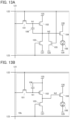
- FIG. 1 is a circuit diagram of a pixel included in a display apparatus according to one embodiment of the present invention.
- a pixel 10 a includes a transistor 101 , a transistor 102 , a transistor 103 , a transistor 104 , a transistor 105 , a capacitor 106 , and a light-emitting device 108 .
- the transistor 101 to the transistor 105 can be n-channel transistors.
- An LED e.g., a micro LED
- One of a source and a drain of the transistor 101 is electrically connected to one electrode of the capacitor 106 and a gate of the transistor 102 .
- One of a source and a drain of the transistor 102 is electrically connected to the other electrode of the capacitor 106 , one of a source and a drain of the transistor 103 , a gate of the transistor 104 , and one of a source and a drain of the transistor 105 .
- One of a source and a drain of the transistor 104 is electrically connected to a cathode of the light-emitting device.
- a point (wiring) where one of the source and the drain of the transistor 101 , the one electrode of the capacitor 106 , and the gate of the transistor 102 are connected is referred to as a node N 1 .
- a point (wiring) where one of the source and the drain of the transistor 102 , the other electrode of the capacitor 106 , one of the source and the drain of the transistor 103 , and one of the source and the drain of the transistor 105 are connected is referred to as a node N 2 .
- the other of the source and the drain of the transistor 101 is electrically connected to a wiring 121 .
- the other of the source and the drain of the transistor 102 is electrically connected to a wiring 125 .
- the other of the source and the drain of the transistor 103 is electrically connected to a wiring 127 .
- the other of the source and the drain of the transistor 104 is electrically connected to a wiring 129 .
- the other of the source and the drain of the transistor 105 is electrically connected to a wiring 128 .
- An anode of the light-emitting device 108 is electrically connected to a wiring 126 .
- a gate of the transistor 101 and a gate of the transistor 105 are electrically connected to a wiring 122 .
- a gate of the transistor 103 is electrically connected to a wiring 123 .
- the wiring 121 is a source line that connects the pixel 10 a to a source driver for supplying image data.
- the wiring 125 , the wiring 126 , the wiring 127 , and the wiring 129 are power supply lines, the wiring 125 and the wiring 126 are high potential power supply lines (the wiring 126 is also referred to as an anode wiring, an anode electrode, or a common electrode), and the wiring 127 and the wiring 129 can be low potential power supply lines (the wiring 129 is also referred to as a cathode wiring).
- the wiring 128 is a wiring for supplying a constant potential.
- the wiring 125 and the wiring 126 may be electrically connected to each other.
- the wiring 127 and the wiring 128 may be electrically connected to each other.
- the wiring 127 , the wiring 128 , and the wiring 129 can be electrically connected to each other.
- Each of the wiring 122 and the wiring 123 is a gate line that controls the operation of a transistor connected thereto.
- the wiring 122 can be electrically connected to a gate driver.
- the wiring 123 can be electrically connected to a ramp wave signal generation circuit.
- the transistor 101 functions as a switch.
- the transistor 102 , the transistor 103 , and the transistor 105 have a function of generating a PWM signal.
- the transistor 104 functions as a driving transistor of the light-emitting device 108 and performs a switching operation in accordance with the generated PWM signal.
- the capacitor 106 functions as a storage capacitor or a bootstrap capacitor.
- the transistor 102 , the transistor 103 , and the transistor 105 are used for generating the PWM signal.
- a high potential (DVDD) for turning on the transistor 104 (the potential can sufficiently reduce on-state resistance) is supplied to the wiring 125 .
- a low potential (DVSS) for turning off the transistor 104 (bringing the transistor 104 in an off state) is supplied to the wiring 127 .
- a low potential (V 0 ) for resetting the potential of the node N 2 is supplied to the wiring 128 . Resetting the node N 2 (the source of the transistor 102 ) to V 0 enables a gate-source voltage (Vgs) of the transistor 102 to be written properly. Note that in order to reset the node N 2 to V 0 surely, the transistor 105 preferably has higher on-state current characteristics than the transistor 103 .
- the maximum value of Vsweep be higher than the maximum value possible for Vdata and the minimum value of Vsweep be lower than the minimum value possible for Vdata.
- the minimum value of Vsweep may be a value with which the transistor 103 is turned off.
- the operation can be expressed as an operation of comparing on-state resistances. That is, when the on-state resistance of the transistor 102 is higher than the on-state resistance of the transistor 103 , the potential of the node N 2 becomes DVDD. In contrast, when the on-state resistance of the transistor 102 is lower than the on-state resistance of the transistor 103 , the potential of the node N 2 becomes DVSS.
- the time during which the potential of the node N 2 becomes DVDD is longer than the time during which it becomes DVSS when Vdata is relatively high, and the time during which the potential of the node N 2 becomes DVSS is longer than the time during which it becomes DVDD when Vdata is relatively low.
- the PWM signals generated with the transistor 102 , the transistor 103 , and the transistor 105 are supplied to the node N 2 .
- FIG. 2 shows the pixels 10 a arranged in a certain column of three consecutive rows (the k-th row, the l-th row, and the m-th row) as targets.
- Vdata_(H, M, or L)-V 0 shown in FIG. 2 corresponds to Vgs of the transistor 102 .
- Vsweep-DVSS corresponds to Vgs of the transistor 103 .
- Vsweep is a signal potential having a ramp wave supplied from the wiring 123
- DVSS is a constant power supply potential supplied to the wiring 127 .
- a waveform of Vsweep-DVSS is equivalent to a waveform of the ramp wave.
- Ramp waves having the same phase are supplied to all the pixels. Accordingly, there is no need to generate ramp waves having different phases for each row, so that a circuit that generates a ramp wave and a circuit that supplies the ramp wave can be simplified.
- the potential of a wiring 122 [ k ] becomes H (high potential)
- the transistor 101 and the transistor 105 are turned on and Vdata_H is supplied to the node N 1
- V 0 is supplied to the node N 2 (see FIG. 4 ).
- Vgs of the transistor 102 becomes Vdata_H-V 0 .
- a ramp wave is supplied to the wiring 123 (see FIG. 4 ).
- the ramp wave can be a triangle wave as shown by Vsweep-DVSS in FIG. 2 .
- the ramp wave can be a sawtooth wave as shown in FIG. 3 A .
- a sine wave, a trapezoidal waveform, or the like can also be used.
- the cycle of the ramp wave can be one frame period at the longest as shown in FIG. 2 . Since Vdata is retained for one frame period, a one-cycle PWM waveform can be generated when the ramp wave cycle is one frame period. When a ramp waveform cycle is one frame period that is the longest cycle, the number of times of charging and discharging of a wiring for supplying a signal potential with a ramp waveform can be minimized, leading to a reduction in power consumption.
- the ramp waveform cycle may be a half-frame period or a quarter-frame period.
- the ramp waveform cycle may be further shortened.
- PWM control adjusts luminance by dividing a lighting period, and lighting and blinking can be repeated at high speed by shortening the ramp waveform cycle, so that afterimages can be suppressed.
- Vdata_H-V 0 is constant; however, Vsweep-DVSS changes over time. Accordingly, the period in which DVSS is supplied to the node N 2 when Vsweep-DVSS>Vdata_H-V 0 (see FIG. 5 ) and the period in which DVDD is supplied to the node N 2 when Vsweep-DVSS ⁇ Vdata_H-V 0 (see FIG. 6 ) are generated.
- Vdata_M is written and Vgs of the transistor 102 becomes Vdata_M-V 0 .
- an operation of comparing Vdata_M-V 0 and Vsweep-DVSS is performed, and the duty ratio is smaller than that in the n ⁇ 1-th frame.
- Vdata_L is written and Vgs of the transistor 102 becomes Vdata_L-V 0 .
- an operation of comparing Vdata_L-V 0 and Vsweep-DVSS is performed, and the duty ratio is smaller than that in the n-th frame and the average current in one frame period is decreased, so that display with low luminance can be performed.
- the timing at which Vsweep-DVSS>Vdata_(H, M, or L)-V 0 is satisfied and the timing at which Vsweep-DVSS ⁇ Vdata_(H, M, or L)-V 0 is satisfied are different even in the case where the same data potential as in the l-th row is written. Note that when the written data potentials are the same, the duty ratios of the generated PWM signals are the same.
- the transistor 101 that writes data to the node N 1 and the transistor 105 that resets the node N 2 are turned on at the same time.
- Vsweep-DVSS ⁇ Vdata_(H, M, or L)-V 0 is satisfied at the time of writing data
- the potential of the node N 2 becomes V 0
- the light-emitting device is turned off in some cases.
- one horizontal period required for writing data is approximately 1/1000 of one frame period when the number of pixels is Full HD, and is approximately 1/2000 of one frame period when the number of pixels is 4K2K.
- the duty ratios of the generated PWM signals are approximately the same.
- an OS transistor a transistor containing a metal oxide in a channel formation region
- the semiconductor layer has a large energy gap, and thus the OS transistor can exhibit characteristics with an extremely low off-state current of several yoctoamperes per micrometer (a current value per micrometer of channel width).
- the gate potential of the transistor 102 can be retained for a long time by the low off-state current characteristics of the OS transistor. Accordingly, an appropriate PWM signal can be generated even when the frame frequency is lowered. For example, switching between the first frame frequency (e.g., higher than or equal to 60 Hz) in moving image display and the second frame frequency that is lower than the first frame frequency (e.g., approximately 1 to 10 Hz) in still image display can reduce power consumption of the display apparatus.
- the first frame frequency e.g., higher than or equal to 60 Hz
- the second frame frequency that is lower than the first frame frequency e.g., approximately 1 to 10 Hz
- a metal oxide whose energy gap is greater than or equal to 2 eV, preferably greater than or equal to 2.5 eV, further preferably greater than or equal to 3 eV can be used.
- a typical example is an oxide semiconductor containing indium, and a CAAC-OS or a CAC-OS, or the like described later can be used, for example.
- a CAAC-OS has a crystal structure including stable atoms and is suitable for a transistor or the like that puts emphasis on reliability.
- a CAC-OS exhibits excellent mobility characteristics and thus is suitable for a transistor or the like that is driven at high speed.
- An OS transistor has features such that impact ionization, an avalanche breakdown, a short-channel effect, and the like do not occur, which are different from those of a transistor where silicon is contained in a channel formation region (hereinafter, a Si transistor), and enables formation of a highly reliable circuit. Moreover, variation in electrical characteristics due to crystallinity unevenness, which is caused in Si transistors, is less likely to occur in OS transistors.
- the atomic ratio of metal elements in a sputtering target used to form the In-M-Zn-based oxide by a sputtering method satisfy In M and Zn M.
- the atomic ratio in the deposited semiconductor layer varies from the atomic ratio of metal elements contained in the sputtering target in a range of ⁇ 40%.
- An oxide semiconductor with low carrier concentration is used for the semiconductor layer.
- Such an oxide semiconductor is referred to as a highly purified intrinsic or substantially highly purified intrinsic oxide semiconductor.
- the oxide semiconductor has low density of defect states and can be referred to as an oxide semiconductor having stable characteristics.
- the composition is not limited to those, and a material having appropriate composition may be used depending on required semiconductor characteristics and electrical characteristics of the transistor (field-effect mobility, threshold voltage, or the like).
- the carrier concentration, impurity concentration, defect density, atomic ratio between a metal element and oxygen, interatomic distance, density, and the like of the semiconductor layer be set to be appropriate.
- the concentration (concentration obtained by secondary ion mass spectrometry) of silicon or carbon in the semiconductor layer is set lower than or equal to 2 ⁇ 10 18 atoms/cm 3 , preferably lower than or equal to 2 ⁇ 10 17 atoms/cm 3 .
- a defect in which hydrogen has entered an oxygen vacancy can function as a donor of the oxide semiconductor.
- the oxide semiconductor is sometimes evaluated by not its donor concentration but its carrier concentration. Therefore, in this specification and the like, the carrier concentration assuming the state where an electric field is not applied is sometimes used, instead of the donor concentration, as the parameter of the oxide semiconductor. That is, “carrier concentration” described in this specification and the like can be replaced with “donor concentration” in some cases.
- the hydrogen concentration in the oxide semiconductor that is obtained by secondary ion mass spectrometry is set lower than 1 ⁇ 10 20 atoms/cm 3 , preferably lower than 1 ⁇ 10 19 atoms/cm 3 , further preferably lower than 5 ⁇ 10 18 atoms/cm 3 , still further preferably lower than 1 ⁇ 10 18 atoms/cm 3 .
- the transistor can have stable electrical characteristics.
- An oxide semiconductor film having an amorphous structure has disordered atomic arrangement and no crystalline component, for example.
- an oxide film having an amorphous structure has a completely amorphous structure and no crystal part.
- CAC Cloud-Aligned Composite
- the CAC-OS is, for example, a composition of a material in which elements that constitute an oxide semiconductor are unevenly distributed to have a size of greater than or equal to 0.5 nm and less than or equal to 10 nm, preferably greater than or equal to 1 nm and less than or equal to 2 nm, or a similar size.
- a state in which one or more metal elements are unevenly distributed and regions including the metal element(s) are mixed to have a size of greater than or equal to 0.5 nm and less than or equal to 10 nm, preferably greater than or equal to 1 nm and less than or equal to 2 nm, or a similar size in an oxide semiconductor is referred to as a mosaic pattern or a patch-like pattern.
- the oxide semiconductor preferably contains at least indium.
- indium and zinc are preferably contained.
- one or a plurality of kinds selected from aluminum, gallium, yttrium, copper, vanadium, beryllium, boron, silicon, titanium, iron, nickel, germanium, zirconium, molybdenum, lanthanum, cerium, neodymium, hafnium, tantalum, tungsten, magnesium, and the like may be contained.
- a CAC-OS in an In—Ga—Zn oxide (an In—Ga—Zn oxide in the CAC-OS may be particularly referred to as CAC-IGZO) has a composition in which materials are separated into indium oxide (hereinafter referred to as InO X1 (X1 is a real number greater than 0)) or indium zinc oxide (hereinafter referred to as In X2 Zn Y2 O Z2 (each of X2, Y2, and Z2 is a real number greater than 0)), and gallium oxide (hereinafter referred to as GaO X3 (X3 is a real number greater than 0)) or gallium zinc oxide (hereinafter referred to as Ga X4 Zn Y4 O Z4 (each of X4, Y4, and Z4 is a real number greater than 0)), so that a mosaic pattern is formed, and mosaic-like InO X1 or In X2 Zn Y2 O Z2 is evenly distributed in the film
- the CAC-OS is a composite oxide semiconductor having a composition in which a region where GaO X3 is a main component and a region where In X2 Zn Y2 O Z2 or InO X1 is a main component are mixed.
- the first region is regarded as having a higher In concentration than the second region.
- IGZO is a commonly known name and sometimes refers to one compound formed of In, Ga, Zn, and O.
- a typical example is a crystalline compound represented by InGaO 3 (ZnO) m1 (m1 is a natural number) or In (1+x0) Ga (1-x0) O 3 (ZnO) m0 ( ⁇ 1 ⁇ x0 ⁇ 1; m0 is a given number).
- the crystalline compound has a single crystal structure, a polycrystalline structure, or a CAAC structure.
- the CAAC structure is a crystal structure in which a plurality of IGZO nanocrystals have c-axis alignment and are connected in an a-b plane without alignment.
- the CAC-OS relates to the material composition of an oxide semiconductor.
- the material composition of a CAC-OS containing In, Ga, Zn, and O some regions that contain Ga as a main component and are observed as nanoparticles and some regions that contain In as a main component and are observed as nanoparticles are each randomly dispersed in a mosaic pattern.
- the crystal structure is a secondary element for the CAC-OS.
- CAC-OS is regarded as not including a stacked-layer structure of two or more kinds of films with different compositions.
- a two-layer structure of a film containing In as a main component and a film containing Ga as a main component is not included.
- the CAC-OS refers to a composition in which some regions that contain the metal element(s) as a main component and are observed as nanoparticles and some regions that contain In as a main component and are observed as nanoparticles are each randomly dispersed in a mosaic pattern.
- the CAC-OS can be formed by a sputtering method under a condition where a substrate is not heated intentionally, for example.
- a sputtering method one or more selected from an inert gas (typically, argon), an oxygen gas, and a nitrogen gas may be used as a deposition gas.
- an inert gas typically, argon
- an oxygen gas typically, an oxygen gas
- a nitrogen gas may be used as a deposition gas.
- the ratio of the flow rate of an oxygen gas to the total flow rate of the deposition gas at the time of deposition is preferably as low as possible, and for example, the ratio of the flow rate of the oxygen gas is preferably higher than or equal to 0% and lower than 30%, further preferably higher than or equal to 0% and lower than or equal to 10%.
- the CAC-OS is characterized in that no clear peak is observed at the time of measurement using ⁇ /2 ⁇ scan by an Out-of-plane method, which is one of the X-ray diffraction (XRD) measurement methods. That is, it is found from X-ray diffraction measurement that no alignment in an a-b plane direction and a c-axis direction is observed in a measured region.
- XRD X-ray diffraction
- the CAC-OS in the In—Ga—Zn oxide has a composition in which regions where GaO X3 is a main component and regions where In X2 Zn Y2 O Z2 or InO X1 is a main component are unevenly distributed and mixed.
- EDX energy dispersive X-ray spectroscopy
- the CAC-OS has a composition different from that of an IGZO compound in which metal elements are evenly distributed, and has characteristics different from those of the IGZO compound. That is, the CAC-OS has a composition in which regions where GaO X3 or the like is a main component and regions where In X2 Zn Y2 O Z2 or InO X1 is a main component are phase-separated from each other, and the regions including the respective elements as the main components form a mosaic pattern.
- a semiconductor device using the CAC-OS has high reliability.
- the CAC-OS is suitable for a constituent material of a variety of semiconductor devices.
- High-quality polycrystalline silicon can be obtained easily by using a laser crystallization step or the like.
- the high-quality polycrystalline silicon can also be obtained by a solid-phase growth method in which a metal catalyst such as nickel or palladium is added to amorphous silicon and then heated.
- a metal catalyst such as nickel or palladium
- the polycrystalline silicon formed by the solid-phase growth method using a metal catalyst may be subjected to laser irradiation. Note that the metal catalyst remains in the polycrystalline silicon and worsens electrical characteristics of the transistor; therefore, it is preferable to provide a region to which phosphorus, a noble gas, or the like is added other than the channel formation region, so that the region captures the metal catalyst.
- Si transistors may be used as all the transistors included in the pixel.
- One or more of the transistors included in the pixel may be p-channel transistors.
- FIG. 7 is a circuit diagram illustrating a pixel 10 b whose configuration is different from that in FIG. 1 .
- the pixel 10 b is different from the pixel 10 a illustrated in FIG. 1 in that the transistor 102 is a p-channel transistor and the transistor 105 is not provided, and in a connection mode of the capacitor 106 .
- the transistor 102 is a p-channel transistor, the source of the transistor 102 is electrically connected to the wiring 125 that supplies a high potential.
- the transistor 105 for resetting the source potential (the potential of the node N 2 ) included in the pixel 10 a can be omitted.
- the other electrode of the capacitor 106 retaining Vgs is electrically connected to the wiring 125 .
- the data potential (Vdata) is supplied to the gate of the transistor 102 (the node N 1 ).
- the signal potential having a ramp wave (Vsweep) is supplied to the gate of the transistor 103 .
- Vsweep changes over time, and when the absolute value of Vdata-DVDD that is Vgs of the transistor 102 is higher than Vsweep-DVSS that is Vgs of the transistor 103 , the potential of the node N 2 becomes DVDD. Thus, the transistor 104 is turned on and the light-emitting device 108 is turned on (emits light). In contrast, when the absolute value of Vdata-DVDD is lower than Vsweep-DVSS, the potential of the node N 2 becomes DVSS. Accordingly, the transistor 104 is turned off and the light-emitting device 108 is turned off.
- the time during which the potential of the node N 2 is DVSS is longer than the time during which it is DVDD when Vdata is relatively low, and the time during which the potential of the node N 2 is DVSS is longer than the time during which it is DVDD when Vdata is relatively high.
- the PWM signals generated with the transistor 102 and the transistor 103 are supplied to the node N 2 .
- the potential of the wiring 122 [ k ] becomes H (high potential)
- the transistor 101 is turned on, and Vdata_H is supplied to the node N 1 (see FIG. 10 ).
- Vgs of the transistor 102 becomes Vdata_H-DVDD.
- the cycle of the ramp wave can be one frame period at the longest as shown in FIG. 8 .
- the ramp waveform cycle may be a half-frame period or a quarter-frame period.
- the ramp waveform cycle may be further shortened.
- Vdata_H-DVDD is constant; however, Vsweep-DVSS changes over time. Accordingly, the period in which DVSS is supplied to the node N 2 when Vsweep-DVSS>
- Vdata_M is written and Vgs of the transistor 102 becomes Vdata_M-DVDD.
- Vdata_M-DVDD As in the description of the n ⁇ 1-th frame, an operation of comparing Vdata_M-DVDD and Vsweep-DVSS is performed, and the duty ratio is larger than that in the n ⁇ 1-th frame.
- Vdata_L is written and Vgs of the transistor 102 becomes Vdata_L-DVDD.
- Vdata_L-DVDD As in the description of the n ⁇ 1-th frame, an operation of comparing Vdata_L-DVDD and Vsweep-DVSS is performed, the duty ratio is larger than that in the n-th frame, and the average current in one frame period is increased, so that display with high luminance can be performed.
- a transistor containing a metal oxide in a channel formation region (hereinafter, an OS transistor) is preferably used as the transistor 101 that is an n-channel transistor as in the pixel 10 a.
- the light-emitting device 108 can be an LED but may be an organic EL element. Note that in the case where an organic EL element is used, the wiring 126 may be electrically connected to one of the source and the drain of the transistor 104 , and the cathode of the light-emitting device 108 may be connected to the other of the source and the drain of the transistor 104 as illustrated in FIG. 13 A and FIG. 13 B . Even in the case where an LED is used as the light-emitting device 108 , configurations illustrated in FIG. 13 A and FIG. 13 B can also be used.
- a configuration with a back gate as illustrated in FIG. 14 A or FIG. 14 B may be employed. Supplying the same potential to the back gate and a front gate can increase on-state current.
- a configuration may be employed in which the back gates can be supplied with a constant potential. Supplying a constant potential to the back gate can control the threshold voltage.
- FIG. 15 is a block diagram illustrating a display apparatus according to one embodiment of the present invention.
- the display apparatus includes a pixel array 11 , a source driver 20 , and a gate driver 30 .
- the pixel array 11 includes pixels 10 arranged in a column direction and a row direction.
- the pixel 10 a or the pixel 10 b described in this embodiment can be used as each of the pixels 10 .
- wirings are illustrated in a simplified way in the drawing, and the wirings connected to the components of the pixel 10 according to one embodiment of the present invention are provided.
- a sequential circuit such as a shift register can be used for the source driver 20 and the gate driver 30 .
- a ramp wave signal generation circuit 40 that generates a triangle wave, a sawtooth wave, or the like is provided and is electrically connected to the pixels 10 .
- the source driver 20 , the gate driver 30 , and the ramp wave signal generation circuit 40 a method in which an IC chip is attached externally by a COF (chip on film) method, a COG (chip on glass) method, a TCP (tape carrier package) method, or the like can be used.
- the source driver 20 , the gate driver 30 , and the ramp wave signal generation circuit may be formed over the same substrate as the pixel array 11 by using transistors manufactured using steps common to those of the pixel array 11 .
- FIG. 16 illustrates a configuration of a pixel PIX used in the simulation.
- the pixel PIX is the same as the pixel circuit illustrated in FIG. 1 , and a transistor Tr 1 to a transistor Tr 5 are n-channel OS transistors.
- a node corresponding to the node N 2 in FIG. 1 is referred to as GPWM.
- a wiring corresponding to the wiring 122 in FIG. 1 is referred to as G 1
- G 2 a wiring corresponding to the wiring 123
- the capacitance value of a capacitor CAP is 100 fF.
- “H” voltage and “L” voltage applied to a gate of the transistor (including a ramp wave) are +15 V and ⁇ 5 V, respectively.
- An anode potential (Vano) is +20 V
- a cathode potential (Vcat) is 0 V
- voltage V 0 is ⁇ 2 V
- voltage DVDD is +12 V
- voltage DVSS is ⁇ 2 V
- Vdata is +2 V to +10 V. Note that SPICE is used as circuit simulation software.
- FIG. 17 A shows simulation results of the voltage of the node N 2 when Vdata is +2 V to +10 V (in 2 V steps) in one frame.
- the horizontal axis represents time (sec), and the case where a ramp wave (a triangle wave) has the maximum value at the center of one frame period is assumed.
- This embodiment can be implemented in an appropriate combination with the structures described in the other embodiments.
- the pixel 10 (the pixel 10 a or the pixel 10 b ) described in Embodiment 1 can be used for the display apparatus described in this embodiment.
- a scan line driver circuit and a signal line driver circuit to be described below correspond to the gate driver and the source driver, respectively.
- FIG. 19 A to FIG. 19 C are diagrams each illustrating a structure of a display apparatus in which one embodiment of the present invention can be used.
- a sealant 4005 is provided to surround a display portion 215 provided over a first substrate 4001 , and the display portion 215 is sealed with the sealant 4005 and a second substrate 4006 .
- a scan line driver circuit 221 a , a signal line driver circuit 231 a , a signal line driver circuit 232 a , and a common line driver circuit 241 a each include a plurality of integrated circuits 4042 provided over a printed circuit board 4041 .
- the integrated circuits 4042 are each formed using a single crystal semiconductor or a polycrystalline semiconductor.
- the common line driver circuit 241 a has a function of supplying a prescribed potential to the wirings 122 , 127 , 128 , 129 , and the like described in Embodiment 1.
- Signals and potentials are supplied to the scan line driver circuit 221 a , the common line driver circuit 241 a , the signal line driver circuit 231 a , and the signal line driver circuit 232 a through an FPC (Flexible printed circuit) 4018 .
- FPC Flexible printed circuit
- the integrated circuits 4042 included in the scan line driver circuit 221 a and the common line driver circuit 241 a each have a function of supplying a selection signal to the display portion 215 .
- the integrated circuits 4042 included in the signal line driver circuit 231 a and the signal line driver circuit 232 a each have a function of supplying image data to the display portion 215 .
- the integrated circuits 4042 are mounted in a region different from the region surrounded by the sealant 4005 over the first substrate 4001 .
- connection method of the integrated circuits 4042 is not particularly limited; a wire bonding method, a COF method, a COG method, a TCP method, or the like can be used.
- FIG. 19 B illustrates an example in which the integrated circuits 4042 included in the signal line driver circuit 231 a and the signal line driver circuit 232 a are mounted by a COG method. Some or all of the driver circuits can be formed over the same substrate as the display portion 215 , so that a system-on-panel can be formed.
- the scan line driver circuit 221 a and the common line driver circuit 241 a are formed over the same substrate as the display portion 215 .
- the driver circuits are formed concurrently with pixel circuits in the display portion 215 , the number of components can be reduced. Accordingly, the productivity can be increased.
- the sealant 4005 is provided to surround the display portion 215 , the scan line driver circuit 221 a , and the common line driver circuit 241 a that are provided over the first substrate 4001 .
- the second substrate 4006 is provided over the display portion 215 , the scan line driver circuit 221 a , and the common line driver circuit 241 a . Consequently, the display portion 215 , the scan line driver circuit 221 a , and the common line driver circuit 241 a are sealed together with the display device by the use of the first substrate 4001 , the sealant 4005 , and the second substrate 4006 .
- the signal line driver circuit 231 a and the signal line driver circuit 232 a are separately formed and mounted on the first substrate 4001 in the example illustrated in FIG. 19 B , one embodiment of the present invention is not limited to this structure.
- the scan line driver circuit may be separately formed and then mounted, or part of the signal line driver circuit or part of the scan line driver circuit may be separately formed and then mounted.
- the signal line driver circuit 231 a and the signal line driver circuit 232 a may be formed over the same substrate as the display portion 215 , as illustrated in FIG. 19 C .
- Examples of a material that can be used for the coloring layer include a metal material, a resin material, and a resin material containing a pigment or a dye.
- the light-blocking layer and the coloring layer can be formed by, for example, an inkjet method or the like.
- the light-emitting device has a microcavity structure
- light with high color purity can be extracted.
- a microcavity structure and a color filter are combined, the glare can be reduced and the visibility of a displayed image can be increased.
- Each of the first electrode layer 4030 and the second electrode layer 4031 can also be formed using one or more kinds selected from a metal such as tungsten (W), molybdenum (Mo), zirconium (Zr), hafnium (Hf), vanadium (V), niobium (Nb), tantalum (Ta), chromium (Cr), cobalt (Co), nickel (Ni), titanium (Ti), platinum (Pt), aluminum (Al), copper (Cu), or silver (Ag); an alloy thereof; and a metal nitride thereof.
- a metal such as tungsten (W), molybdenum (Mo), zirconium (Zr), hafnium (Hf), vanadium (V), niobium (Nb), tantalum (Ta), chromium (Cr), cobalt (Co), nickel (Ni), titanium (Ti), platinum (Pt), aluminum (Al), copper (Cu), or silver (Ag); an alloy thereof; and a
- a stacked-layer structure including the semiconductor layer 4610 , the light-emitting layer 4620 , and the semiconductor layer 4630 is formed to emit red light, green light, blue light, bluish violet light, violet light, ultraviolet light, or the like.
- a compound containing a Group 13 element and a Group 15 element also referred to as a Group III-V compound
- Examples of the Group 13 element include aluminum, gallium, and indium.
- Examples of the Group 15 element include nitrogen, phosphorus, arsenic, and antimony.
- a material such as gallium nitride can be used for a light-emitting diode emitting light in the ultraviolet wavelength range to the blue wavelength range.
- a material such as a compound of indium and gallium nitride can be used for a light-emitting diode emitting light in the ultraviolet wavelength range to the green wavelength range.
- a material such as a compound of aluminum, gallium, indium, and phosphorus or a compound of gallium and arsenic can be used for a light-emitting diode emitting light in the green wavelength range to the red wavelength range.
- a material such as a compound of gallium and arsenic can be used for a light-emitting diode emitting light in the infrared wavelength range.
- a color image can be displayed without using a color conversion layer. Accordingly, a step of forming a color conversion layer is unnecessary, and manufacturing cost of the display apparatus can be reduced.
- a structure may be employed in which all micro LEDs 4600 provided over the same plane emit light of the same color.
- light emitted from the light-emitting layer 4620 is extracted to the outside of the display apparatus through one or both of a color conversion layer and a coloring layer.
- Quantum dots can be used for the color conversion layer, for example.
- the semiconductor layer 4630 is electrically connected to a wiring layer 4730 through a wiring layer 4710 and a wiring layer 4720 .
- the wiring layer 4730 can supply a cathode potential.
- a protective circuit for protecting the driver circuit is preferably provided.
- the protective circuit is preferably formed using a nonlinear element.
- the structure illustrated in FIG. 22 can also be used for a backlight of a liquid crystal display apparatus. Overlapping the structure illustrated in FIG. 22 and a pixel including a liquid crystal element can perform local dimming drive, so that display with an extremely high contrast is possible.
- This embodiment can be implemented in an appropriate combination with the structures described in the other embodiments.
- the display apparatus can be manufactured using a transistor with various modes, such as a bottom-gate transistor or a top-gate transistor. Therefore, the material of a semiconductor layer and the structure of a transistor can be easily changed depending on the existing production line.
- FIG. 23 A is a cross-sectional view of a channel-protective transistor 810 , which is a kind of bottom-gate transistor, in a channel length direction.
- the transistor 810 is formed over a substrate 771 .
- the transistor 810 includes an electrode 746 over the substrate 771 with an insulating layer 772 therebetween.
- the transistor 810 further includes a semiconductor layer 742 over the electrode 746 with an insulating layer 726 therebetween.
- the electrode 746 can function as a gate electrode.
- the insulating layer 726 can function as a gate insulating layer.
- an insulating layer 741 is provided over a channel formation region in the semiconductor layer 742 .
- an electrode 744 a and an electrode 744 b are provided over the insulating layer 726 to be partly in contact with the semiconductor layer 742 .
- the electrode 744 a can function as one of a source electrode and a drain electrode.
- the electrode 744 b can function as the other of the source electrode and the drain electrode. Part of the electrode 744 a and part of the electrode 744 b are formed over the insulating layer 741 .
- the insulating layer 741 can function as a channel protective layer. With the insulating layer 741 provided over the channel formation region, the semiconductor layer 742 can be prevented from being exposed at the time of forming the electrode 744 a and the electrode 744 b . Thus, the channel formation region in the semiconductor layer 742 can be prevented from being etched at the time of forming the electrode 744 a and the electrode 744 b.
- the transistor 810 includes an insulating layer 728 over the electrode 744 a , the electrode 744 b , and the insulating layer 741 and further includes an insulating layer 729 over the insulating layer 728 .
- a material capable of removing oxygen from part of the semiconductor layer 742 to generate oxygen vacancies is preferably used at least for portions of the electrode 744 a and the electrode 744 b that are in contact with the semiconductor layer 742 .
- a carrier concentration is increased; thus, the region becomes n-type to be an n-type region (n+ region). Accordingly, the region can function as a source region or a drain region.
- examples of the material capable of removing oxygen from the semiconductor layer 742 to generate oxygen vacancies include tungsten and titanium.
- a layer that functions as an n-type semiconductor or a p-type semiconductor is preferably provided between the semiconductor layer 742 and the electrode 744 a and between the semiconductor layer 742 and the electrode 744 b .
- the layer that functions as an n-type semiconductor or a p-type semiconductor can function as the source region or the drain region in the transistor.
- the insulating layer 729 is preferably formed using a material that has a function of preventing or reducing diffusion of impurities into the transistor from the outside. Note that the insulating layer 729 can be omitted as necessary.
- An electrode 723 that can function as a back gate electrode is provided over the insulating layer 729 .
- the electrode 723 can be formed using a material and a method similar to those for the electrode 746 . Note that a structure in which the electrode 723 is not provided may be employed.
- a back gate electrode is formed using a conductive layer and positioned so that a channel formation region in a semiconductor layer is sandwiched between the gate electrode and the back gate electrode.
- the back gate electrode can function in a manner similar to that of the gate electrode.
- the potential of the back gate electrode may be equal to the potential of the gate electrode or may be a ground potential (GND potential) or a given potential.
- GND potential ground potential
- the threshold voltage of the transistor can be changed.
- the electrode 746 and the electrode 723 can each function as a gate electrode.
- the insulating layer 726 , the insulating layer 728 , and the insulating layer 729 can each function as a gate insulating layer.
- the electrode 723 may be provided between the insulating layer 728 and the insulating layer 729 .
- the other is referred to as a “back gate electrode.”
- the electrode 746 is referred to as a “back gate electrode.”
- the transistor 810 can be regarded as a kind of top-gate transistor.
- one of the electrode 746 and the electrode 723 is referred to as a “first gate electrode,” and the other is referred to as a “second gate electrode.”
- the electrode 746 and the electrode 723 With the electrode 746 and the electrode 723 with the semiconductor layer 742 sandwiched therebetween and setting the potential of the electrode 746 equal to the potential of the electrode 723 , a region of the semiconductor layer 742 through which carriers flow is enlarged in a film thickness direction; thus, the amount of transferred carriers is increased. As a result, the on-state current of the transistor 810 is increased and the field-effect mobility is increased.
- the transistor 810 is a transistor having high on-state current for its occupation area. That is, the occupation area of the transistor 810 can be small for required on-state current.
- the gate electrode and the back gate electrode are formed using conductive layers and thus each have a function of preventing an electric field generated outside the transistor from affecting the semiconductor layer in which the channel is formed (in particular, an electric field blocking function against static electricity and the like). Note that when the back gate electrode is formed larger than the semiconductor layer so that the semiconductor layer is covered with the back gate electrode, the electric field blocking function can be enhanced.
- the back gate electrode is formed using a light-blocking conductive film
- light can be prevented from entering the semiconductor layer from the back gate electrode side. Therefore, photodegradation of the semiconductor layer can be prevented, and degradation in electrical characteristics of the transistor, such as a shift in the threshold voltage, can be prevented.
- FIG. 23 B is a cross-sectional view of a channel-protective transistor 820 , which has a structure different from FIG. 23 A , in a channel length direction.
- the transistor 820 has substantially the same structure as the transistor 810 but is different from the transistor 810 in that the insulating layer 741 covers end portions of the semiconductor layer 742 .
- the semiconductor layer 742 is electrically connected to the electrode 744 a through an opening portion formed by selectively removing part of the insulating layer 741 that overlaps with the semiconductor layer 742 .
- the semiconductor layer 742 is electrically connected to the electrode 744 b through another opening portion formed by selectively removing part of the insulating layer 741 that overlaps with the semiconductor layer 742 .
- a region of the insulating layer 741 that overlaps with the channel formation region can function as a channel protective layer.
- the semiconductor layer 742 can be prevented from being exposed at the time of forming the electrode 744 a and the electrode 744 b .
- the semiconductor layer 742 can be prevented from being reduced in thickness at the time of forming the electrode 744 a and the electrode 744 b.
- the distance between the electrode 744 a and the electrode 746 and the distance between the electrode 744 b and the electrode 746 are longer in the transistor 820 than in the transistor 810 .
- parasitic capacitance generated between the electrode 744 a and the electrode 746 can be reduced.
- parasitic capacitance generated between the electrode 744 b and the electrode 746 can be reduced.
- FIG. 23 C is a cross-sectional view of a channel-etched transistor 825 , which is a kind of bottom-gate transistor, in a channel length direction.
- the electrode 744 a and the electrode 744 b are formed without the insulating layer 741 .
- part of the semiconductor layer 742 that is exposed at the time of forming the electrode 744 a and the electrode 744 b might be etched.
- the productivity of the transistor can be increased.
- a transistor 842 illustrated in FIG. 24 A is a kind of top-gate transistor.
- the electrode 744 a and the electrode 744 b are electrically connected to the semiconductor layer 742 through opening portions formed in the insulating layer 728 and the insulating layer 729 .
- the transistor 842 includes the electrode 723 that is formed over the substrate 771 .
- the electrode 723 includes a region overlapping with the semiconductor layer 742 with the insulating layer 772 therebetween.
- the electrode 723 can function as a back gate electrode. Note that a structure in which the electrode 723 is not provided may be employed.
- an electric field for inducing a channel can be effectively applied to the semiconductor layer 742 by one or both of the gate electrode and the back gate electrode, which enables the transistor to have an improved current drive capability and high on-state current characteristics.
- the transistor can be miniaturized because the on-state current can be increased.
- the S-channel structure can also increase the mechanical strength of the transistor.
- FIG. 26 D illustrates a dashboard camera, which includes a housing 931 , a display portion 932 , operation buttons 933 , microphones 934 , a lens 935 , an attaching member 936 , and the like.
- the dashboard camera is mounted to the windshield or the like of a motor vehicle by the attaching member 936 so that the dashboard camera can record a front view during driving. An image being recorded can be displayed on the display portion 932 .
- the display apparatus according to one embodiment of the present invention can be employed for the display portion 932 .
Landscapes
- Engineering & Computer Science (AREA)
- Physics & Mathematics (AREA)
- General Physics & Mathematics (AREA)
- Theoretical Computer Science (AREA)
- Microelectronics & Electronic Packaging (AREA)
- Computer Hardware Design (AREA)
- Geometry (AREA)
- Electroluminescent Light Sources (AREA)
- Control Of Indicators Other Than Cathode Ray Tubes (AREA)
- Manufacturing & Machinery (AREA)
Abstract
Description
-
- [Patent Document 1] Specification of United States Patent Application Publication No. 2014/0367705
- [Patent Document 2] Japanese Published Patent Application No. 2007-123861
- [Patent Document 3] Japanese Published Patent Application No. 2007-96055
-
- Tr1: transistor, Tr2: transistor, Tr3: transistor, Tr4: transistor, Tr5: transistor, 10: pixel, 10 a: pixel, 10 b: pixel, 11: pixel array, 20: source driver, 30: gate driver, 40: ramp wave signal generation circuit, 101: transistor, 102: transistor, 103: transistor, 104: transistor, 105: transistor, 106: capacitor, 108: light-emitting device, 121: wiring, 122: wiring, 123: wiring, 125: wiring, 126: wiring, 127: wiring, 128: wiring, 129: wiring, 215: display portion, 221 a: scan line driver circuit, 231 a: signal line driver circuit, 232 a: signal line driver circuit, 241 a: common line driver circuit, 723: electrode, 726: insulating layer, 728: insulating layer, 729: insulating layer, 741: insulating layer, 742: semiconductor layer, 744 a: electrode, 744 b: electrode, 746: electrode, 771: substrate, 772: insulating layer, 810: transistor, 820: transistor, 825: transistor, 842: transistor, 844: transistor, 846: transistor, 911: housing, 912: display portion, 913: speaker, 914: operation button, 919: camera, 921: pillar, 922: display portion, 931: housing, 932: display portion, 933: operation button, 934: microphone, 935: lens, 936: member, 951: housing, 952: display portion, 953: operation button, 954: external connection port, 955: speaker, 956: microphone, 957: camera, 961: housing, 962: shutter button, 963: microphone, 965: display portion, 966: operation key, 967: speaker, 968: zoom lever, 969: lens, 971: housing, 973: display portion, 974: operation button, 975: speaker, 976: communication connection terminal, 977: optical sensor, 4001: substrate, 4005: sealant, 4006: substrate, 4010: transistor, 4011: transistor, 4014: wiring, 4015: electrode, 4018: FPC, 4019: anisotropic conductive layer, 4020: capacitor, 4021: electrode, 4030: electrode layer, 4031: electrode layer, 4041: printed circuit board, 4042: integrated circuit, 4104: insulating layer, 4110: insulating layer, 4111: insulating layer, 4112: insulating layer, 4200: input device, 4210: touch panel, 4227: electrode, 4228: electrode, 4237: wiring, 4238: wiring, 4239: wiring, 4263: substrate, 4272 b: FPC, 4273 b: IC, 4510: partition, 4511: light-emitting layer, 4513: light-emitting device, 4514: filler, 4600: micro LED, 4610: semiconductor layer, 4620: light-emitting layer, 4630: semiconductor layer, 4710: wiring layer, 4720: wiring layer, 4730: wiring layer
Claims (10)
Applications Claiming Priority (3)
| Application Number | Priority Date | Filing Date | Title |
|---|---|---|---|
| JP2020-166887 | 2020-10-01 | ||
| JP2020166887 | 2020-10-01 | ||
| PCT/IB2021/058328 WO2022069980A1 (en) | 2020-10-01 | 2021-09-14 | Display apparatus and electronic equipment |
Related Parent Applications (1)
| Application Number | Title | Priority Date | Filing Date |
|---|---|---|---|
| PCT/IB2021/058328 A-371-Of-International WO2022069980A1 (en) | 2020-10-01 | 2021-09-14 | Display apparatus and electronic equipment |
Related Child Applications (1)
| Application Number | Title | Priority Date | Filing Date |
|---|---|---|---|
| US19/238,722 Continuation US20250309210A1 (en) | 2020-10-01 | 2025-06-16 | Display apparatus and electronic device |
Publications (2)
| Publication Number | Publication Date |
|---|---|
| US20230335050A1 US20230335050A1 (en) | 2023-10-19 |
| US12355019B2 true US12355019B2 (en) | 2025-07-08 |
Family
ID=80951384
Family Applications (2)
| Application Number | Title | Priority Date | Filing Date |
|---|---|---|---|
| US18/026,634 Active US12355019B2 (en) | 2020-10-01 | 2021-09-14 | Display apparatus and electronic device |
| US19/238,722 Pending US20250309210A1 (en) | 2020-10-01 | 2025-06-16 | Display apparatus and electronic device |
Family Applications After (1)
| Application Number | Title | Priority Date | Filing Date |
|---|---|---|---|
| US19/238,722 Pending US20250309210A1 (en) | 2020-10-01 | 2025-06-16 | Display apparatus and electronic device |
Country Status (5)
| Country | Link |
|---|---|
| US (2) | US12355019B2 (en) |
| JP (2) | JPWO2022069980A1 (en) |
| KR (1) | KR20230078700A (en) |
| CN (1) | CN116324956A (en) |
| WO (1) | WO2022069980A1 (en) |
Citations (43)
| Publication number | Priority date | Publication date | Assignee | Title |
|---|---|---|---|---|
| US20020105506A1 (en) * | 2001-02-07 | 2002-08-08 | Ikuo Hiyama | Image display system and image information transmission method |
| US20030058687A1 (en) | 2001-09-21 | 2003-03-27 | Hajime Kimura | Semiconductor device |
| US20030103022A1 (en) | 2001-11-09 | 2003-06-05 | Yukihiro Noguchi | Display apparatus with function for initializing luminance data of optical element |
| WO2003052728A1 (en) | 2001-12-14 | 2003-06-26 | Sanyo Electric Co., Ltd. | Digitally driven type display device |
| JP2004198683A (en) | 2002-12-18 | 2004-07-15 | Semiconductor Energy Lab Co Ltd | Display device |
| EP1439520A2 (en) | 2003-01-20 | 2004-07-21 | SANYO ELECTRIC Co., Ltd. | Display device of active matrix drive type |
| US20050062106A1 (en) * | 2003-09-08 | 2005-03-24 | Yukihiro Noguchi | Luminance adjusting display apparatus |
| CN1698084A (en) | 2001-12-14 | 2005-11-16 | 三洋电机株式会社 | digital drive display |
| US20060125412A1 (en) * | 2004-12-13 | 2006-06-15 | Au Optronics Corp. | Pixel driving circuit and pixel driving method |
| CN1901008A (en) | 2005-07-21 | 2007-01-24 | 精工爱普生株式会社 | Electronic circuit, electronic device, method of driving electronic device, electro-optical device, and electronic apparatus |
| KR20070012232A (en) | 2005-07-21 | 2007-01-25 | 세이코 엡슨 가부시키가이샤 | Electronic circuits, electronic devices, methods of driving electronic devices, electro-optical devices and electronic devices |
| US7180245B2 (en) * | 2003-06-11 | 2007-02-20 | Semiconductor Energy Laboratory Co., Ltd. | Light emitting device and element substrate |
| JP2007096055A (en) | 2005-09-29 | 2007-04-12 | Semiconductor Energy Lab Co Ltd | Semiconductor device and manufacturing method of semiconductor device |
| JP2007123861A (en) | 2005-09-29 | 2007-05-17 | Semiconductor Energy Lab Co Ltd | Semiconductor device and manufacturing method thereof |
| US20070236440A1 (en) * | 2006-04-06 | 2007-10-11 | Emagin Corporation | OLED active matrix cell designed for optimal uniformity |
| US20080203930A1 (en) | 2005-05-19 | 2008-08-28 | Koninklijke Philips Electronics, N.V. | Electroluminescent Display Devices |
| US20090121642A1 (en) | 2007-11-14 | 2009-05-14 | Infineon Techologies Ag | Organic Light Emitting Diode Driver |
| US7674650B2 (en) | 2005-09-29 | 2010-03-09 | Semiconductor Energy Laboratory Co., Ltd. | Semiconductor device and manufacturing method thereof |
| JP2011039540A (en) | 2010-09-24 | 2011-02-24 | Semiconductor Energy Lab Co Ltd | Display device |
| US20110050761A1 (en) | 2009-08-26 | 2011-03-03 | Nec Electronics Corporation | Pixel circuit and display device |
| US20130082906A1 (en) | 2011-09-30 | 2013-04-04 | Sony Corporation | Pixel circuit, pixel circuit driving method, display apparatus, and electronic device |
| US20140367705A1 (en) | 2013-06-17 | 2014-12-18 | LuxVue Technology Corporation | Reflective bank structure and method for integrating a light emitting device |
| US20150243220A1 (en) | 2014-02-25 | 2015-08-27 | Lg Display Co., Ltd. | Display Backplane and Method of Fabricating the Same |
| US20160096725A1 (en) * | 2014-10-07 | 2016-04-07 | Semiconductor Energy Laboratory Co., Ltd. | Semiconductor device, display module, and electronic device |
| US20180182294A1 (en) * | 2016-12-22 | 2018-06-28 | Intel Corporation | Low power dissipation pixel for display |
| US20180197474A1 (en) * | 2017-01-06 | 2018-07-12 | Samsung Display Co., Ltd. | Organic light emitting display apparatus |
| US20180240421A1 (en) * | 2017-02-17 | 2018-08-23 | Semiconductor Energy Laboratory Co., Ltd. | Display device |
| US20180293929A1 (en) | 2017-04-11 | 2018-10-11 | Samsung Electronics Co., Ltd. | Pixel circuit of display panel and display device |
| US20180301080A1 (en) * | 2017-04-13 | 2018-10-18 | Samsung Electronics Co., Ltd. | Display panel and driving method of display panel |
| US10395594B1 (en) | 2015-09-18 | 2019-08-27 | Apple Inc. | Hybrid microdriver and TFT architecture |
| US10455653B1 (en) * | 2018-08-09 | 2019-10-22 | Innolux Corporation | LED driving circuits |
| WO2019220275A1 (en) | 2018-05-18 | 2019-11-21 | 株式会社半導体エネルギー研究所 | Display device, and drive method for display device |
| US20190371231A1 (en) | 2018-05-31 | 2019-12-05 | Samsung Electronics Co., Ltd. | Display panel and method for driving the display panel |
| US20200043405A1 (en) * | 2018-07-31 | 2020-02-06 | Nichia Corporation | Image display device |
| US20210065616A1 (en) | 2019-08-30 | 2021-03-04 | Samsung Display Co., Ltd. | Pixel circuit |
| US20210158747A1 (en) | 2018-05-17 | 2021-05-27 | Semiconductor Energy Laboratory Co., Ltd. | Display panel, display device, input/output device, and data processing device |
| US20210174734A1 (en) | 2017-12-25 | 2021-06-10 | Semiconductor Energy Laboratory Co., Ltd. | Display and electronic device including the display |
| US20210407380A1 (en) | 2019-11-01 | 2021-12-30 | Boe Technology Group Co., Ltd. | Pixel driving circuit and driving method thereof, and display panel |
| US20220005790A1 (en) | 2018-09-07 | 2022-01-06 | Semiconductor Energy Laboratory Co., Ltd. | Display device, display module, and electronic device |
| US20220068197A1 (en) * | 2020-08-28 | 2022-03-03 | Samsung Electronics Co., Ltd. | Display apparatus and control method thereof |
| US20220199001A1 (en) * | 2020-12-18 | 2022-06-23 | Lx Semicon Co., Ltd. | LED Driving Circuit, Display Panel, and Pixel Driving Device |
| WO2023079404A1 (en) | 2021-11-05 | 2023-05-11 | 株式会社半導体エネルギー研究所 | Display device and electronic equipment |
| US11783760B2 (en) * | 2021-09-09 | 2023-10-10 | Wuhan China Star Optoelectronics Semiconductor Display Technology Co., Ltd. | Pixel circuit and display panel |
Family Cites Families (3)
| Publication number | Priority date | Publication date | Assignee | Title |
|---|---|---|---|---|
| GB0412586D0 (en) * | 2004-06-05 | 2004-07-07 | Koninkl Philips Electronics Nv | Active matrix display devices |
| TW201706978A (en) * | 2015-08-04 | 2017-02-16 | 啟耀光電股份有限公司 | Display panel and pixel circuit |
| US11132941B2 (en) * | 2019-12-24 | 2021-09-28 | Au Optronics Corporation | Display panel and pixel circuit thereof |
-
2021
- 2021-09-14 WO PCT/IB2021/058328 patent/WO2022069980A1/en not_active Ceased
- 2021-09-14 US US18/026,634 patent/US12355019B2/en active Active
- 2021-09-14 CN CN202180064067.XA patent/CN116324956A/en active Pending
- 2021-09-14 JP JP2022553231A patent/JPWO2022069980A1/ja active Pending
- 2021-09-14 KR KR1020237012277A patent/KR20230078700A/en active Pending
-
2025
- 2025-06-16 US US19/238,722 patent/US20250309210A1/en active Pending
-
2026
- 2026-01-08 JP JP2026002005A patent/JP2026063007A/en active Pending
Patent Citations (61)
| Publication number | Priority date | Publication date | Assignee | Title |
|---|---|---|---|---|
| US20020105506A1 (en) * | 2001-02-07 | 2002-08-08 | Ikuo Hiyama | Image display system and image information transmission method |
| US20030058687A1 (en) | 2001-09-21 | 2003-03-27 | Hajime Kimura | Semiconductor device |
| US20030103022A1 (en) | 2001-11-09 | 2003-06-05 | Yukihiro Noguchi | Display apparatus with function for initializing luminance data of optical element |
| US20050156828A1 (en) * | 2001-12-14 | 2005-07-21 | Atsuhiro Yamashita | Display device of digital drive type |
| WO2003052728A1 (en) | 2001-12-14 | 2003-06-26 | Sanyo Electric Co., Ltd. | Digitally driven type display device |
| JP2003241711A (en) | 2001-12-14 | 2003-08-29 | Sanyo Electric Co Ltd | Digitally driven type display device |
| US7358935B2 (en) | 2001-12-14 | 2008-04-15 | Sanyo Electric Co., Ltd. | Display device of digital drive type |
| EP1455335A1 (en) | 2001-12-14 | 2004-09-08 | Sanyo Electric Co., Ltd. | Digitally driven type display device |
| CN1698084A (en) | 2001-12-14 | 2005-11-16 | 三洋电机株式会社 | digital drive display |
| JP2004198683A (en) | 2002-12-18 | 2004-07-15 | Semiconductor Energy Lab Co Ltd | Display device |
| EP1439520A2 (en) | 2003-01-20 | 2004-07-21 | SANYO ELECTRIC Co., Ltd. | Display device of active matrix drive type |
| US20040207614A1 (en) | 2003-01-20 | 2004-10-21 | Atsuhiro Yamashita | Display device of active matrix drive type |
| JP2004246320A (en) | 2003-01-20 | 2004-09-02 | Sanyo Electric Co Ltd | Active matrix drive type display device |
| US7180245B2 (en) * | 2003-06-11 | 2007-02-20 | Semiconductor Energy Laboratory Co., Ltd. | Light emitting device and element substrate |
| US20050062106A1 (en) * | 2003-09-08 | 2005-03-24 | Yukihiro Noguchi | Luminance adjusting display apparatus |
| US20060125412A1 (en) * | 2004-12-13 | 2006-06-15 | Au Optronics Corp. | Pixel driving circuit and pixel driving method |
| US20080203930A1 (en) | 2005-05-19 | 2008-08-28 | Koninklijke Philips Electronics, N.V. | Electroluminescent Display Devices |
| JP2008541185A (en) | 2005-05-19 | 2008-11-20 | コーニンクレッカ フィリップス エレクトロニクス エヌ ヴィ | Electroluminescent display device |
| CN1901008A (en) | 2005-07-21 | 2007-01-24 | 精工爱普生株式会社 | Electronic circuit, electronic device, method of driving electronic device, electro-optical device, and electronic apparatus |
| US8144081B2 (en) | 2005-07-21 | 2012-03-27 | Seiko Epson Corporation | Electronic circuit, electronic device, method of driving electronic device, electro-optical device, and electronic apparatus |
| JP2007025523A (en) | 2005-07-21 | 2007-02-01 | Seiko Epson Corp | Electronic device, electro-optical device and electronic apparatus |
| US7639211B2 (en) | 2005-07-21 | 2009-12-29 | Seiko Epson Corporation | Electronic circuit, electronic device, method of driving electronic device, electro-optical device, and electronic apparatus |
| US20070018078A1 (en) * | 2005-07-21 | 2007-01-25 | Seiko Epson Corporation | Electronic circuit, electronic device, method of driving electronic device, electro-optical device, and electronic apparatus |
| KR20070012232A (en) | 2005-07-21 | 2007-01-25 | 세이코 엡슨 가부시키가이샤 | Electronic circuits, electronic devices, methods of driving electronic devices, electro-optical devices and electronic devices |
| US7674650B2 (en) | 2005-09-29 | 2010-03-09 | Semiconductor Energy Laboratory Co., Ltd. | Semiconductor device and manufacturing method thereof |
| JP2007123861A (en) | 2005-09-29 | 2007-05-17 | Semiconductor Energy Lab Co Ltd | Semiconductor device and manufacturing method thereof |
| JP2007096055A (en) | 2005-09-29 | 2007-04-12 | Semiconductor Energy Lab Co Ltd | Semiconductor device and manufacturing method of semiconductor device |
| US20070236440A1 (en) * | 2006-04-06 | 2007-10-11 | Emagin Corporation | OLED active matrix cell designed for optimal uniformity |
| WO2007120475A2 (en) | 2006-04-06 | 2007-10-25 | Emagin Corporation | Oled active matrix cell designed for optimal uniformity |
| DE102008054150A1 (en) | 2007-11-14 | 2009-05-28 | Infineon Technologies Ag | Driver for an organic light-emitting diode |
| CN101437341A (en) | 2007-11-14 | 2009-05-20 | 英飞凌科技股份有限公司 | Organic light emitting diode driver |
| US20090121642A1 (en) | 2007-11-14 | 2009-05-14 | Infineon Techologies Ag | Organic Light Emitting Diode Driver |
| US20110050761A1 (en) | 2009-08-26 | 2011-03-03 | Nec Electronics Corporation | Pixel circuit and display device |
| JP2011039540A (en) | 2010-09-24 | 2011-02-24 | Semiconductor Energy Lab Co Ltd | Display device |
| JP2013076812A (en) | 2011-09-30 | 2013-04-25 | Sony Corp | Pixel circuit, pixel circuit driving method, display apparatus, and electronic device |
| CN103035189A (en) | 2011-09-30 | 2013-04-10 | 索尼公司 | Pixel circuit, pixel circuit driving method, display apparatus, and electronic device |
| US20130082906A1 (en) | 2011-09-30 | 2013-04-04 | Sony Corporation | Pixel circuit, pixel circuit driving method, display apparatus, and electronic device |
| US20140367705A1 (en) | 2013-06-17 | 2014-12-18 | LuxVue Technology Corporation | Reflective bank structure and method for integrating a light emitting device |
| US20150243220A1 (en) | 2014-02-25 | 2015-08-27 | Lg Display Co., Ltd. | Display Backplane and Method of Fabricating the Same |
| US20160096725A1 (en) * | 2014-10-07 | 2016-04-07 | Semiconductor Energy Laboratory Co., Ltd. | Semiconductor device, display module, and electronic device |
| US10395594B1 (en) | 2015-09-18 | 2019-08-27 | Apple Inc. | Hybrid microdriver and TFT architecture |
| US20180182294A1 (en) * | 2016-12-22 | 2018-06-28 | Intel Corporation | Low power dissipation pixel for display |
| US20180197474A1 (en) * | 2017-01-06 | 2018-07-12 | Samsung Display Co., Ltd. | Organic light emitting display apparatus |
| US20180240421A1 (en) * | 2017-02-17 | 2018-08-23 | Semiconductor Energy Laboratory Co., Ltd. | Display device |
| US20180293929A1 (en) | 2017-04-11 | 2018-10-11 | Samsung Electronics Co., Ltd. | Pixel circuit of display panel and display device |
| US20180301080A1 (en) * | 2017-04-13 | 2018-10-18 | Samsung Electronics Co., Ltd. | Display panel and driving method of display panel |
| US20210174734A1 (en) | 2017-12-25 | 2021-06-10 | Semiconductor Energy Laboratory Co., Ltd. | Display and electronic device including the display |
| US20210158747A1 (en) | 2018-05-17 | 2021-05-27 | Semiconductor Energy Laboratory Co., Ltd. | Display panel, display device, input/output device, and data processing device |
| TW202004723A (en) | 2018-05-18 | 2020-01-16 | 日商半導體能源研究所股份有限公司 | Display device, and drive method for display device |
| WO2019220275A1 (en) | 2018-05-18 | 2019-11-21 | 株式会社半導体エネルギー研究所 | Display device, and drive method for display device |
| US20210366368A1 (en) * | 2018-05-18 | 2021-11-25 | Semiconductor Energy Laboratory Co., Ltd. | Display device and method for driving display device |
| US20190371231A1 (en) | 2018-05-31 | 2019-12-05 | Samsung Electronics Co., Ltd. | Display panel and method for driving the display panel |
| US20200043405A1 (en) * | 2018-07-31 | 2020-02-06 | Nichia Corporation | Image display device |
| US10455653B1 (en) * | 2018-08-09 | 2019-10-22 | Innolux Corporation | LED driving circuits |
| US20220005790A1 (en) | 2018-09-07 | 2022-01-06 | Semiconductor Energy Laboratory Co., Ltd. | Display device, display module, and electronic device |
| US20210065616A1 (en) | 2019-08-30 | 2021-03-04 | Samsung Display Co., Ltd. | Pixel circuit |
| US20210407380A1 (en) | 2019-11-01 | 2021-12-30 | Boe Technology Group Co., Ltd. | Pixel driving circuit and driving method thereof, and display panel |
| US20220068197A1 (en) * | 2020-08-28 | 2022-03-03 | Samsung Electronics Co., Ltd. | Display apparatus and control method thereof |
| US20220199001A1 (en) * | 2020-12-18 | 2022-06-23 | Lx Semicon Co., Ltd. | LED Driving Circuit, Display Panel, and Pixel Driving Device |
| US11783760B2 (en) * | 2021-09-09 | 2023-10-10 | Wuhan China Star Optoelectronics Semiconductor Display Technology Co., Ltd. | Pixel circuit and display panel |
| WO2023079404A1 (en) | 2021-11-05 | 2023-05-11 | 株式会社半導体エネルギー研究所 | Display device and electronic equipment |
Non-Patent Citations (4)
| Title |
|---|
| Goshi Biwa et al., "Commercialization of the Crystal LED Display System Using Micro LEDs to Realize Scalable and High-Quality Images", The Journal of The Institute of Image Information and Television Engineers 2020, vol. 74, No. 1, pp. 174-179, The Institute of Image Information and Television Engineers. |
| International Search Report (Application No. PCT/IB2021/058328) Dated Dec. 21, 2021. |
| Wang. T et al., "A New PWM Pixel Circuit for Micro-LED Displaly with 60Hz Driving and 120Hz Lighting", SID Digest '20 : SID International Symposium Digest of Technical Papers, Sep. 25, 2020, vol. 51, No. 1, pp. 1707-1710. |
| Written Opinion (Application No. PCT/IB2021/058328) Dated Dec. 21, 2021. |
Also Published As
| Publication number | Publication date |
|---|---|
| US20230335050A1 (en) | 2023-10-19 |
| CN116324956A (en) | 2023-06-23 |
| US20250309210A1 (en) | 2025-10-02 |
| WO2022069980A1 (en) | 2022-04-07 |
| KR20230078700A (en) | 2023-06-02 |
| JPWO2022069980A1 (en) | 2022-04-07 |
| JP2026063007A (en) | 2026-04-10 |
Similar Documents
| Publication | Publication Date | Title |
|---|---|---|
| US12272700B2 (en) | Display apparatus and electronic device | |
| US12446309B2 (en) | Display device and electronic device | |
| US12387680B2 (en) | Display apparatus, its operating method, and electronic device | |
| US11694594B2 (en) | Display device, driving method of display device, and electronic device | |
| US11508307B2 (en) | Method for operating display device | |
| JP2025114815A (en) | display device | |
| US12089459B2 (en) | Display apparatus and electronic device | |
| US12355019B2 (en) | Display apparatus and electronic device |
Legal Events
| Date | Code | Title | Description |
|---|---|---|---|
| AS | Assignment |
Owner name: SEMICONDUCTOR ENERGY LABORATORY CO., LTD., JAPAN Free format text: ASSIGNMENT OF ASSIGNORS INTEREST;ASSIGNORS:KAWASHIMA, SUSUMU;KUSUNOKI, KOJI;WATANABE, KAZUNORI;AND OTHERS;REEL/FRAME:063002/0106 Effective date: 20230301 |
|
| FEPP | Fee payment procedure |
Free format text: ENTITY STATUS SET TO UNDISCOUNTED (ORIGINAL EVENT CODE: BIG.); ENTITY STATUS OF PATENT OWNER: LARGE ENTITY |
|
| STPP | Information on status: patent application and granting procedure in general |
Free format text: NON FINAL ACTION MAILED |
|
| STPP | Information on status: patent application and granting procedure in general |
Free format text: RESPONSE TO NON-FINAL OFFICE ACTION ENTERED AND FORWARDED TO EXAMINER |
|
| STPP | Information on status: patent application and granting procedure in general |
Free format text: FINAL REJECTION MAILED |
|
| STPP | Information on status: patent application and granting procedure in general |
Free format text: DOCKETED NEW CASE - READY FOR EXAMINATION |
|
| STPP | Information on status: patent application and granting procedure in general |
Free format text: NON FINAL ACTION MAILED |
|
| STPP | Information on status: patent application and granting procedure in general |
Free format text: RESPONSE TO NON-FINAL OFFICE ACTION ENTERED AND FORWARDED TO EXAMINER |
|
| STPP | Information on status: patent application and granting procedure in general |
Free format text: FINAL REJECTION MAILED |
|
| STPP | Information on status: patent application and granting procedure in general |
Free format text: RESPONSE AFTER FINAL ACTION FORWARDED TO EXAMINER |
|
| STPP | Information on status: patent application and granting procedure in general |
Free format text: NOTICE OF ALLOWANCE MAILED -- APPLICATION RECEIVED IN OFFICE OF PUBLICATIONS |
|
| STCF | Information on status: patent grant |
Free format text: PATENTED CASE |