US12348251B2 - Method and system for multi-band digital pre-distortion using a canonical form with reduced dimension look-up table - Google Patents
Method and system for multi-band digital pre-distortion using a canonical form with reduced dimension look-up table Download PDFInfo
- Publication number
- US12348251B2 US12348251B2 US17/358,062 US202117358062A US12348251B2 US 12348251 B2 US12348251 B2 US 12348251B2 US 202117358062 A US202117358062 A US 202117358062A US 12348251 B2 US12348251 B2 US 12348251B2
- Authority
- US
- United States
- Prior art keywords
- dpd
- band
- linear
- polynomial
- dimensional
- Prior art date
- Legal status (The legal status is an assumption and is not a legal conclusion. Google has not performed a legal analysis and makes no representation as to the accuracy of the status listed.)
- Active, expires
Links
Images


Classifications
-
- H—ELECTRICITY
- H03—ELECTRONIC CIRCUITRY
- H03F—AMPLIFIERS
- H03F1/00—Details of amplifiers with only discharge tubes, only semiconductor devices or only unspecified devices as amplifying elements
- H03F1/32—Modifications of amplifiers to reduce non-linear distortion
- H03F1/3241—Modifications of amplifiers to reduce non-linear distortion using predistortion circuits
- H03F1/3252—Modifications of amplifiers to reduce non-linear distortion using predistortion circuits using multiple parallel paths between input and output
-
- H—ELECTRICITY
- H04—ELECTRIC COMMUNICATION TECHNIQUE
- H04B—TRANSMISSION
- H04B1/00—Details of transmission systems, not covered by a single one of groups H04B3/00 - H04B13/00; Details of transmission systems not characterised by the medium used for transmission
- H04B1/02—Transmitters
- H04B1/04—Circuits
- H04B1/0475—Circuits with means for limiting noise, interference or distortion
-
- H—ELECTRICITY
- H03—ELECTRONIC CIRCUITRY
- H03F—AMPLIFIERS
- H03F1/00—Details of amplifiers with only discharge tubes, only semiconductor devices or only unspecified devices as amplifying elements
- H03F1/32—Modifications of amplifiers to reduce non-linear distortion
- H03F1/3241—Modifications of amplifiers to reduce non-linear distortion using predistortion circuits
- H03F1/3247—Modifications of amplifiers to reduce non-linear distortion using predistortion circuits using feedback acting on predistortion circuits
-
- H—ELECTRICITY
- H03—ELECTRONIC CIRCUITRY
- H03F—AMPLIFIERS
- H03F1/00—Details of amplifiers with only discharge tubes, only semiconductor devices or only unspecified devices as amplifying elements
- H03F1/32—Modifications of amplifiers to reduce non-linear distortion
- H03F1/3241—Modifications of amplifiers to reduce non-linear distortion using predistortion circuits
- H03F1/3258—Modifications of amplifiers to reduce non-linear distortion using predistortion circuits based on polynomial terms
-
- H—ELECTRICITY
- H03—ELECTRONIC CIRCUITRY
- H03F—AMPLIFIERS
- H03F3/00—Amplifiers with only discharge tubes or only semiconductor devices as amplifying elements
- H03F3/189—High-frequency amplifiers, e.g. radio frequency amplifiers
- H03F3/19—High-frequency amplifiers, e.g. radio frequency amplifiers with semiconductor devices only
- H03F3/195—High-frequency amplifiers, e.g. radio frequency amplifiers with semiconductor devices only in integrated circuits
-
- H—ELECTRICITY
- H03—ELECTRONIC CIRCUITRY
- H03F—AMPLIFIERS
- H03F3/00—Amplifiers with only discharge tubes or only semiconductor devices as amplifying elements
- H03F3/20—Power amplifiers, e.g. Class B amplifiers, Class C amplifiers
- H03F3/24—Power amplifiers, e.g. Class B amplifiers, Class C amplifiers of transmitter output stages
- H03F3/245—Power amplifiers, e.g. Class B amplifiers, Class C amplifiers of transmitter output stages with semiconductor devices only
-
- H—ELECTRICITY
- H03—ELECTRONIC CIRCUITRY
- H03F—AMPLIFIERS
- H03F2200/00—Indexing scheme relating to amplifiers
- H03F2200/111—Indexing scheme relating to amplifiers the amplifier being a dual or triple band amplifier, e.g. 900 and 1800 MHz, e.g. switched or not switched, simultaneously or not
-
- H—ELECTRICITY
- H03—ELECTRONIC CIRCUITRY
- H03F—AMPLIFIERS
- H03F2200/00—Indexing scheme relating to amplifiers
- H03F2200/451—Indexing scheme relating to amplifiers the amplifier being a radio frequency amplifier
-
- H—ELECTRICITY
- H03—ELECTRONIC CIRCUITRY
- H03F—AMPLIFIERS
- H03F2201/00—Indexing scheme relating to details of amplifiers with only discharge tubes, only semiconductor devices or only unspecified devices as amplifying elements covered by H03F1/00
- H03F2201/32—Indexing scheme relating to modifications of amplifiers to reduce non-linear distortion
- H03F2201/3233—Adaptive predistortion using lookup table, e.g. memory, RAM, ROM, LUT, to generate the predistortion
Definitions
- FIG. 1 shows a non-linear system 100 .
- the non-linear system 100 e.g., a digital-to-analog converter (DAC), a power amplifier, etc.
- DAC digital-to-analog converter
- output signal z(n) Due to the non-linear effects of the non-linear system 100 , non-linear distortions such as harmonics and intermodulation may be present at the output signal z(n).
- the DPD circuitry 210 may implement a mathematical model that produces an approximation of the inverse function of the non-linear system 220 . By pre-distorting the input signal to the non-linear system 220 the non-linear effects of the non-linear system 220 can be compensated and the output of the non-linear system 220 may be linearized.
- the non-linear system 220 may be modeled using polynomials or piece-wise polynomial functions to characterize the non-linear response of the system.
- the terms (e.g., polynomial terms) of the mathematical model for the DPD typically resemble that of the non-linearity with different parameters.
- Polynomial-based DPD systems receive input samples and applies the polynomial functions of the model to the input samples to generate pre-distorted DPD outputs. More specifically, the polynomial DPD systems may evaluate each of a set of polynomials given one or more input samples, apply the polynomial outputs as a non-linear gain factor to a function of the input samples, and sum the resulting samples to generate the DPD output.
- the pre-distorted outputs may represent the inverse of the actual non-linearities of the non-linear system, which may be substantially canceled when the DPD outputs are applied as input to the non-linear system.
- Polynomial-based DPD systems may either depend only on the current input sample (i.e., a memoryless polynomial model) or may depend on the current input sample in addition to one or more past input samples (i.e., a polynomial model with memory).
- the polynomial models with memory may present the DPD model as the sum of a plurality of terms, where each term is the product of a function of the current and/or previous input samples and a polynomial that is a function of the magnitude or power of the current or previous input samples.
- a DPD polynomial model with memory may evaluate each of a set of polynomials at one or more input samples, apply each polynomial output as a gain factor to a function of one or more input samples, and sum the resulting products to produce the overall DPD output.
- a DPD polynomial model may need to evaluate each of the set of polynomials in order to produce each DPD output sample.
- polynomial DPD systems may utilize one or more look-up tables (LUTs) to generate the DPD outputs.
- LUTs look-up tables
- DPD LUT systems may evaluate each of the polynomials over a wide range of input samples and may store the resulting outputs in a separate LUT.
- the LUT-based DPD systems may evaluate each LUT according to the received input samples and produce an LUT output value for each LUT.
- the LUT-based DPD systems may then produce the DPD output by applying the LUT output values as a set of gains to the corresponding function of input samples, thus avoiding direct evaluation of each polynomial.
- the DPD system 210 may utilize adaptable LUTs that dynamically adjust the LUT coefficients for each LUT based on feedback from the output of the non-linear system 220 .
- a DPD adaptation circuit (not shown) may perform adaptation of the LUT coefficients utilizing the feedback information derived from the output of the non-linear system 220 .
- the DPD adaptation circuit may be a part of the DPD system 210 .
- the DPD adaptation circuit may attempt to correct for any inaccuracies in the LUT coefficients that are observable through non-linearities detected in the output of the non-linear system 220 .
- the DPD adaptation circuit may employ an adaptation scheme such as Least Squares (LS) based on either indirect or direct learning to adapt the LUT coefficients of the DPD system 210 . Therefore, the DPD system 210 may dynamically adapt the LUT coefficients over time based on observations of the output of the non-linear system 220 .
- LS Least Squares
- multi-band DPD is implemented for a non-linear system using a combination of a LUT that evaluates a non-linear function and computation of terms of a non-linear polynomial.
- the DPD circuitry 210 may be configured to perform multi-band DPD on a multi-band input signal to compensate for a non-linearity of a non-linear system.
- the multi-band input signal includes inputs signals of multiple frequency bands.
- the DPD circuitry 210 may perform DPD on an input signal of each frequency band per frequency band.
- the input signal of each frequency band is modified (pre-distorted) by the DPD circuitry 210 , and the pre-distorted input signals of the multiple frequency bands may be combined at the output of the DPD circuitry 210 .
- the non-linear polynomial may be a linear combination of basis functions.
- Each basis function may be a symmetrical multi-dimensional polynomial taking, as input variables, a magnitude or power of input signals of frequency bands other than an input signal of a frequency band on which the DPD is performed.
- some of the multi-dimensional polynomials are proportional to the magnitude of one of the bands. In this trivial case, use of look-up table is not needed.
- the non-linear polynomial may be decomposed to a canonical form.
- the entries of the LUT may be reduced or minimized (the LUT may have entries in a coarse granularity) and the DPD circuitry 210 may perform interpolation or extrapolation based on the entries of the LUT (e.g., two consecutive entries of the LUT).
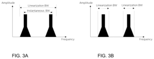
- a multi-band DPD may be implemented either using a wide bandwidth and a high sampling rate DPD where the entire spectrum spanning all frequency bands is linearized (wideband DPD) or using a multi-band DPD model at a lower sampling rate where only spectrum within each band is linearized, and outside of each band is ignored (filtered by band filters).
- FIGS. 3 A and 3 B illustrate the wideband DPD and multi-band DPD schemes, respectively.
- the linearization bandwidth covers the instantaneous bandwidth (i.e., from the lower edge of the lowest carrier to the upper edge of the highest carrier) plus extra spectrum to cover the spectral regrowth around the transmitted RF carriers.
- the DPD scheme linearizes inside each frequency band. Assuming that the bandwidth of the carrier is relatively small compared to the instantaneous bandwidth this could result in a significant reduction in processing sample rate.
- each band contains a carrier of 200 MHz bandwidth, and spectral regrowth occurs up to fifth order intermodulation (IM5).
- each band may be corrected separately using multi-dimensional algorithm (band 2 interferes non-linearly with band 1 and vice versa).
- the linearization bandwidth is 40 MHz ⁇ 5, a minimum sampling rate of 200 MSPS. There are two such bands processed simultaneously, resulting in 400 MSPS total sample throughput. That is almost 1 ⁇ 3 of the wideband algorithm. The larger the ratio of instantaneous bandwidth to carrier bandwidth, the larger the reduction in total sample rate using a multiband algorithm.
- FIG. 4 is a diagram of a system for performing multi-band DPD using multi-dimensional LUTs.
- FIG. 4 shows a two-band case as an example.
- the system includes a DPD circuitry 410 .
- the input samples x 1 and x 2 402 a , 402 b of the two frequency bands are received by the DPD circuitry 410 .
- the DPD circuitry 410 includes 2D LUTs 416 in this example. In case of N frequency bands, N-dimensional LUTs may be used.
- the magnitude (or alternatively, the power) of the input signals x 1 and x 2 402 a , 402 b are computed by the magnitude (or power) calculation units 412 and the magnitude (or power) values of the input samples of the two bands are used to address the 2D LUTs 416 .
- Delay networks 414 are also provided to distribute the magnitude (power) values to the LUTs 416 and to synchronize the input signal 402 a , 402 b and the LUT outputs.
- the LUT outputs are multiplied by a multiplier 418 with the input sample 402 a , 402 b (x 1 or x 2 ), respectively, and summed by the summing network 420 to generate a DPD output y 1 and y 2 , respectively.
- the (pre-distorted) DPD outputs on the two bands are further processed for transmission (e.g., mixed for up-conversion by a mixer, summed, and amplified by an amplifier and sent to antenna for transmission.)
- the transmit signal is tapped onto the observation receiver 440 as a feedback signal and the feedback signal is processed by the DPD adaptation circuitry 450 for updating the LUT values.
- i 1 k 1 - i 1 + 1
- i 2 k 2 - i 2
- i B k B - i B
- ⁇ i 1 k 1 + 1 2
- y 6 35 u 3 +140( v 3 +w 3 )+420( u 2 v+u 2 w )+630( uv 2 +uw 2 )+1260( v 2 w+vw 2 )+2520 uvw
- y 6 35 u 3 +140(( v+w ) 3 ⁇ 3 v 2 w ⁇ 3 vw 2 )+420 u 2 ( v+w )+630 u (( v+w ) 2 ⁇ 2 vw )+1260 vw ( v+w )+2520 uvw
- y 6 35 u 3 +140( v+w ) 3 +420 u 2 ( v+w )+630 u ( v+w ) 2 +840 vw ( v+w )+1260 uvw
- y 6 (35 u 3 )+
- f ( u,v,w ) ⁇ 0 + ⁇ 2 y 2 + ⁇ 4 y 4 +a 6 y 6
- f ( u,v,w ) ⁇ 0 + ⁇ 2 (3 u+ 6( v+w ))+ ⁇ 4 ((10 u 2 )+( v+w )(60 u )+( v+w ) 2 (30)+ vw (60))+ ⁇ 6 ((35 u 3 )+( v+w )(420 u 2 )+( v+w ) 2 (630 u )+( v+w ) 3 (140)+ vw (1260 u )+ vw ( v+w )(840)).
- f ( u,v,w ) ( ⁇ 0 +3 ⁇ 2 u+ 10 ⁇ 4 u 2 +35 ⁇ 6 u 3 )+( v+w )(6 ⁇ 2 +60 ⁇ 4 u+ 420 ⁇ 6 u 2 )+( v+w ) 2 (30 ⁇ 4 +630 ⁇ 6 u )+( v+w ) 3 (140 ⁇ 6 )+ vw (60 ⁇ 4 +1260 ⁇ 6 u )+ vw ( v+w )(840 ⁇ 6 ).
- the above canonical form greatly reduces the number of LUTs from 16 to 6, by only introducing an extra add (v+w) and one extra multiplication (vw).
- FIG. 10 is a flow diagram of a example process for multi-band DPD for a non-linear system.
- a multi-band input signal including input signals of multiple frequency bands is received ( 1002 ).
- Multi-band DPD is performed on the multi-band input signal to compensate for a non-linearity of a non-linear system ( 1004 ).
- DPD is performed on an input signal of each frequency band per frequency band.
- the DPD is performed using a combination of a LUT that evaluates a non-linear function and computation of terms of a non-linear polynomial of one or more variables representing the input signals of multiple frequency bands, wherein both the non-linear function and the non-linear polynomial are in a reduced dimension lower than a dimension of the multi-band input signal.
- application processor 1105 may include, for example, one or more CPU cores and one or more of cache memory, low drop-out voltage regulators (LDOs), interrupt controllers, serial interfaces such as serial peripheral interface (SPI), inter-integrated circuit (I2C) or universal programmable serial interface module, real time clock (RTC), timer-counters including interval and watchdog timers, general purpose input-output (IO), memory card controllers such as secure digital/multi-media card (SD/MMC) or similar, universal serial bus (USB) interfaces, mobile industry processor interface (MIPI) interfaces and Joint Test Access Group (JTAG) test access ports.
- LDOs low drop-out voltage regulators
- interrupt controllers serial interfaces such as serial peripheral interface (SPI), inter-integrated circuit (I2C) or universal programmable serial interface module, real time clock (RTC), timer-counters including interval and watchdog timers, general purpose input-output (IO), memory card controllers such as secure digital/multi-media card (SD/MMC)
- application processor 1205 may include one or more CPU cores and one or more of cache memory, low drop-out voltage regulators (LDOs), interrupt controllers, serial interfaces such as SPI, I2C or universal programmable serial interface module, real time clock (RTC), timer-counters including interval and watchdog timers, general purpose IO, memory card controllers such as SD/MMC or similar, USB interfaces, MIPI interfaces and Joint Test Access Group (JTAG) test access ports.
- LDOs low drop-out voltage regulators
- interrupt controllers serial interfaces such as SPI, I2C or universal programmable serial interface module
- RTC real time clock
- timer-counters including interval and watchdog timers
- general purpose IO memory card controllers such as SD/MMC or similar
- USB interfaces such as SD/MMC or similar
- MIPI interfaces Joint Test Access Group (JTAG) test access ports.
- JTAG Joint Test Access Group
- power management integrated circuitry 1225 may include one or more of voltage regulators, surge protectors, power alarm detection circuitry and one or more backup power sources such as a battery or capacitor.
- Power alarm detection circuitry may detect one or more of brown out (under-voltage) and surge (over-voltage) conditions.
- power tee circuitry 1230 may provide for electrical power drawn from a network cable to provide both power supply and data connectivity to the base station radio head 1200 using a single cable.
- network controller 1235 may provide connectivity to a network using a standard network interface protocol such as Ethernet.
- Network connectivity may be provided using a physical connection which is one of electrical (commonly referred to as copper interconnect), optical or wireless.
- satellite navigation receiver module 1245 may include circuitry to receive and decode signals transmitted by one or more navigation satellite constellations such as the global positioning system (GPS), Globalnaya Navigatsionnaya Sputnikovaya Sistema (GLONASS), Galileo and/or BeiDou.
- the receiver 1245 may provide data to application processor 1205 which may include one or more of position data or time data.
- Application processor 1205 may use time data to synchronize operations with other radio base stations.
- user interface 1250 may include one or more of physical or virtual buttons, such as a reset button, one or more indicators such as light emitting diodes (LEDs) and a display screen.
- buttons such as a reset button
- indicators such as light emitting diodes (LEDs) and a display screen.
- Another example is a computer program having a program code for performing at least one of the methods described herein, when the computer program is executed on a computer, a processor, or a programmable hardware component.
- Another example is a machine-readable storage including machine readable instructions, when executed, to implement a method or realize an apparatus as described herein.
- a further example is a machine-readable medium including code, when executed, to cause a machine to perform any of the methods described herein.
- An example (e.g., example 1) relates to a system for multi-band DPD for a non-linear system.
- the system includes a DPD circuitry configured to perform multi-band DPD on a multi-band input signal to compensate for a non-linearity of a non-linear system.
- the multi-band input signal includes input signals of multiple frequency bands and the DPD circuitry is configured to perform DPD on an input signal of each frequency band per frequency band.
- the DPD circuitry may be configured to perform the DPD using a combination of a LUT that evaluates a non-linear function and computation of terms of a non-linear polynomial of one or more variables representing the input signals of multiple frequency bands, wherein both the non-linear function and the non-linear polynomial are in a reduced dimension lower than a dimension of the multi-band input signal.
- Another example relates to a previously described example (e.g., example 1), wherein the non-linear polynomial is a linear combination of basis functions, wherein each basis function is a symmetrical multi-dimensional polynomial taking, as input variables, a magnitude or power of input signals of frequency bands other than an input signal of a frequency band on which the DPD is performed.
- the non-linear polynomial is a linear combination of basis functions, wherein each basis function is a symmetrical multi-dimensional polynomial taking, as input variables, a magnitude or power of input signals of frequency bands other than an input signal of a frequency band on which the DPD is performed.
- Another example (e.g., example 3) relates to a previously described example (e.g., example 2), wherein the symmetrical multi-dimensional polynomial is proportional to a magnitude of one of the frequency bands other than the frequency band on which DPD is performed.
- Another example (e.g., example 4) relates to a previously described example (e.g., any one of examples 1-3), wherein the non-linear polynomial is in a canonical form.
- Another example (e.g., example 5) relates to a previously described example (e.g., any one of examples 1-4), wherein the DPD circuitry is configured to perform interpolation or extrapolation based on the LUT.
- Another example (e.g., example 6) relates to a previously described example (e.g., any one of examples 1-5), wherein the DPD circuitry is configured to perform a three-dimensional multi-band DPD using both a two-dimensional LUT and computation of one-dimensional polynomial terms.
- Another example (e.g., example 7) relates to a previously described example (e.g., any one of examples 1-6), wherein the DPD circuitry is configured to perform a three-dimensional multi-band DPD using both one-dimensional LUTs and computation of two-dimensional polynomial terms.
- Another example (e.g., example 8) relates to a method for multi-band DPD for a non-linear system.
- the method includes receiving a multi-band input signal including input signals of multiple frequency bands, and performing multi-band DPD on the multi-band input signal to compensate for a non-linearity of a non-linear system.
- the DPD may be performed on an input signal of each frequency band per frequency band.
- the DPD may be performed using a combination of a LUT that evaluates a non-linear function and computation of terms of a non-linear polynomial of one or more variables representing the input signals of multiple frequency bands, wherein both the non-linear function and the non-linear polynomial are in a reduced dimension lower than a dimension of the multi-band input signal.
- Another example (e.g., example 9) relates to a previously described example (e.g., example 8), wherein the non-linear polynomial is a linear combination of basis functions, wherein each basis function is a symmetrical multi-dimensional polynomial taking, as input variables, a magnitude or power of input signals of frequency bands other than an input signal of a frequency band on which the DPD is performed.
- the non-linear polynomial is a linear combination of basis functions, wherein each basis function is a symmetrical multi-dimensional polynomial taking, as input variables, a magnitude or power of input signals of frequency bands other than an input signal of a frequency band on which the DPD is performed.
- Examples may further be or relate to a computer program having a program code for performing one or more of the above methods, when the computer program is executed on a computer or processor. Steps, operations or processes of various above-described methods may be performed by programmed computers or processors. Examples may also cover program storage devices such as digital data storage media, which are machine, processor or computer readable and encode machine-executable, processor-executable or computer-executable programs of instructions. The instructions perform or cause performing some or all of the acts of the above-described methods.
- the program storage devices may comprise or be, for instance, digital memories, magnetic storage media such as magnetic disks and magnetic tapes, hard drives, or optically readable digital data storage media.
- a functional block denoted as “means for . . . ” performing a certain function may refer to a circuit that is configured to perform a certain function.
- a “means for s.th.” may be implemented as a “means configured to or suited for s.th.”, such as a device or a circuit configured to or suited for the respective task.
- Functions of various elements shown in the figures may be implemented in the form of dedicated hardware, such as “a signal provider”, “a signal processing unit”, “a processor”, “a controller”, etc. as well as hardware capable of executing software in association with appropriate software.
- a processor the functions may be provided by a single dedicated processor, by a single shared processor, or by a plurality of individual processors, some of which or all of which may be shared.
- processor or “controller” is by far not limited to hardware exclusively capable of executing software but may include digital signal processor (DSP) hardware, network processor, application specific integrated circuit (ASIC), field programmable gate array (FPGA), read only memory (ROM) for storing software, random access memory (RAM), and non-volatile storage.
- DSP digital signal processor
- ASIC application specific integrated circuit
- FPGA field programmable gate array
- ROM read only memory
- RAM random access memory
- non-volatile storage Other hardware, conventional and/or custom, may also be included.
- a block diagram may, for instance, illustrate a high-level circuit diagram implementing the principles of the disclosure.
- a flow chart, a flow diagram, a state transition diagram, a pseudo code, and the like may represent various processes, operations or steps, which may, for instance, be substantially represented in computer readable medium and so executed by a computer or processor, whether or not such computer or processor is explicitly shown.
- Methods disclosed in the specification or in the claims may be implemented by a device having means for performing each of the respective acts of these methods.
- each claim may stand on its own as a separate example. While each claim may stand on its own as a separate example, it is to be noted that—although a dependent claim may refer in the claims to a specific combination with one or more other claims—other examples may also include a combination of the dependent claim with the subject matter of each other dependent or independent claim. Such combinations are explicitly proposed herein unless it is stated that a specific combination is not intended. Furthermore, it is intended to include also features of a claim to any other independent claim even if this claim is not directly made dependent to the independent claim.
Landscapes
- Engineering & Computer Science (AREA)
- Power Engineering (AREA)
- Physics & Mathematics (AREA)
- Nonlinear Science (AREA)
- Signal Processing (AREA)
- Computer Networks & Wireless Communication (AREA)
- General Physics & Mathematics (AREA)
- Mathematical Analysis (AREA)
- Mathematical Optimization (AREA)
- Pure & Applied Mathematics (AREA)
- Algebra (AREA)
- Microelectronics & Electronic Packaging (AREA)
- Amplifiers (AREA)
Abstract
Description
f(u 1 ,u 2 , . . . ,u B)=Σk
where B is the number of frequency bands, and uk=|xk|2 or |xk| where xk is input samples on band k. In an example for three bands, the 3D LUT function may be written as:
f(u,v,w)=Σi,j,k a i,j,k u i v j w k. Equation (2)
f(u,v,w)=Σk w k(Σi,j a i,j,k u i v i), Equation (3)
f(u,v,w)=Σk w k g k(u,v), Equation (4)
where gk(u,v) may be implemented with 2D LUTs.
f(u,v,w)=Σj,k v j w k(Σiαi,j,k u i), Equation (5)
f(u,v,w)=Σj,k v j w k g j,k(u), Equation (6)
wherein gk(u) may be implemented with 1D LUTs.
f(u,v,w)=Σi,j(v+w)i(vw)i g i,j(u), Equation (7)
where gk(u) may be implemented with 1D LUTs.
x n=2 Re(Σ1≤b≤B x b,n)=Σ1≤b≤B(x b,n +x b,n*), Equation (8)
where B is the number of bands.
x b(t)=x b BB(t)e jω
where BB refers to baseband. The discrete time version of the RF signal for band b is (sampling period Ts):
x b,n =x b,n BB e j
y=Σ pαp x p. Equation (11)
where f(2p+1)(u1, u2, . . . , uB)=Σk
a k
y 1=Σpα2p+1 x 2p+1=(Σpα2p+1 f (2p+1)(u 1 ,u 2 , . . . ,u B))x 1 =f(u 1 ,u 2 , . . . ,u B)x 1, Equation (20)
where
y n=ΣmΣpαm,p x n−m p. Equation (21)
y n=Σm f m(u 1 ,u 2 , . . . ,u B)x 1,n−m, Equation (22)
where
f(|x 1,n−l|2 ,|x 2,n−l|2 ,|x 3,n−l|2)x 2,n−l 5 x 3,n*3, Equation (23)
where f(⋅) is of the form:
f(u 1 ,u 2 , . . . ,u B)=Σk
where uk=|xk|2.
f(u,v,w)=Σi,j,k a i,j,k u i v i w k. Equation (26)
f(u,v,w)=Σk w k(Σi,jαi,j,k u i v j)⇒f(u,v,w)=Σk w k g k(u,v). Equation (27)
f(u,v,w)=Σj,k v j w k(Σiαi,j,k u i), Equation (28)
f(u,v,w)=Σj,k v j w k g j,k(u). Equation (29)
y=Σ pα2p y 2p x 1, Equation (30)
y 2p =x 2p=Σk
where
y 6=35u 3+140(v 3 +w 3)+420(u 2 v+u 2 w)+630(uv 2 +uw 2)+1260(v 2 w+vw 2)+2520uvw,
y 6=35u 3+140((v+w)3−3v 2 w−3vw 2)+420u 2(v+w)+630u((v+w)2−2vw)+1260vw(v+w)+2520uvw,
y 6=35u 3+140(v+w)3+420u 2(v+w)+630u(v+w)2+840vw(v+w)+1260uvw,
y 6=(35u 3)+(v+w)(420u 2)+(v+w)2(630u)+(v+w)3(140)+vw(1260u)+vw(v+w)(840).
f(u,v,w)=α0+α2 y 2+α4 y 4 +a 6 y 6,
f(u,v,w)=α0+α2(3u+6(v+w))+α4((10u 2)+(v+w)(60u)+(v+w)2(30)+vw(60))+α6((35u 3)+(v+w)(420u 2)+(v+w)2(630u)+(v+w)3(140)+vw(1260u)+vw(v+w)(840)).
f(u,v,w)=(α0+3α2 u+10α4 u 2+35α6 u 3)+(v+w)(6α2+60α4 u+420α6 u 2)+(v+w)2(30α4+630α6 u)+(v+w)3(140α6)+vw(60α4+1260α6 u)+vw(v+w)(840α6).
f(u,v,w)=Σi,jΣi,j(v+w)i(v w)j g i,j(u),
g 0,0(u)=α0+3α2 u+10α4 u 2+35α6 u 3,
g 1,0(u)=6α2+60α4 u+420α6 u 2,
g 2,0(u)=30α4+630α6 u,
g 3,0(u)=140α6,
g 0,1(u)=60α4+1260α6 u,
g 1,1(u)=840α6.
f(u,v,w)=Σi,j v i w i g i,j(u),
where i and j can each take 4 values, leading to 16 possible combinations or 16 1D LUTs.
X l=Σ(p
where O(l)=(1, . . . 1) (l element vector), Z(l)=(0, . . . 0) (B−1−l element vector), B is the number of bands, the function H denotes a set of permutations: H(k1, . . . , kM), the set of all unique permutations of k1, . . . , kM.
Π(7,0,0)={(7,0,0),(0,7,0),(0,0,7)},
Π(5,1,1)={(5,1,1),(1,5,1),(1,1,5)}
Π(5,2,0)={(5,2,0),(5,0,2),(2,5,0),(0,5,2),(2,0,5),(0,2,5)},
H(2,2,2)={(2,2,2)}.
f(u 1 , . . . ,u B)=Σl
| TABLE 1 | |||
| B = 2 | B = 3 | B = 4 | B > 4 |
| l1 ≤ K | l1 + 2l2 ≤ K | l1 + 2l2 + 3l3 ≤ K | l1 + 2l2 + 3l3 ≤ K |
| and lq = 0 for q > 3 | |||
| l1 | l1, l2 | l1, l2, l3 | l1, l2, l3, l4 = . . . = |
| lB−1 = 0 | |||
| 0 | 0 0 | 0 0 0 | 0 0 0 0 . . . 0 |
| 1 | 0 1 | 0 0 1 | 0 0 1 0 . . . 0 |
| 2 | 1 0 | 0 1 0 | 0 1 0 0 . . . 0 |
| 3 | 1 1 | 1 0 0 | 1 0 0 0 . . . 0 |
| 2 0 | 1 1 0 | 1 1 0 0 . . . 0 | |
| 3 0 | 2 0 0 | 2 0 0 0 . . . 0 | |
| 3 0 0 | 3 0 0 0 . . . 0 | ||
| N1DLUT = 4 | N1DLUT = 6 | N1DLUT =7 | N1DLUT = 7 |
Claims (15)
Priority Applications (2)
| Application Number | Priority Date | Filing Date | Title |
|---|---|---|---|
| US17/358,062 US12348251B2 (en) | 2021-06-25 | 2021-06-25 | Method and system for multi-band digital pre-distortion using a canonical form with reduced dimension look-up table |
| EP22180519.5A EP4109749A1 (en) | 2021-06-25 | 2022-06-22 | Method and system for multi-band digital pre-distortion using a canonical form with reduced dimension look-up table |
Applications Claiming Priority (1)
| Application Number | Priority Date | Filing Date | Title |
|---|---|---|---|
| US17/358,062 US12348251B2 (en) | 2021-06-25 | 2021-06-25 | Method and system for multi-band digital pre-distortion using a canonical form with reduced dimension look-up table |
Publications (2)
| Publication Number | Publication Date |
|---|---|
| US20220416823A1 US20220416823A1 (en) | 2022-12-29 |
| US12348251B2 true US12348251B2 (en) | 2025-07-01 |
Family
ID=82214256
Family Applications (1)
| Application Number | Title | Priority Date | Filing Date |
|---|---|---|---|
| US17/358,062 Active 2043-11-02 US12348251B2 (en) | 2021-06-25 | 2021-06-25 | Method and system for multi-band digital pre-distortion using a canonical form with reduced dimension look-up table |
Country Status (2)
| Country | Link |
|---|---|
| US (1) | US12348251B2 (en) |
| EP (1) | EP4109749A1 (en) |
Families Citing this family (4)
| Publication number | Priority date | Publication date | Assignee | Title |
|---|---|---|---|---|
| JP7692468B2 (en) * | 2020-09-08 | 2025-06-13 | インターディジタル・シーイー・パテント・ホールディングス・ソシエテ・パ・アクシオンス・シンプリフィエ | DEVICE AND METHOD FOR APPLYING A LOOKUP TABLE - Patent application |
| CN116471153B (en) * | 2023-05-25 | 2025-09-05 | 华中科技大学 | Digital predistortion method based on block uniform mapping lookup table with bilinear interpolation |
| WO2025012675A1 (en) * | 2023-07-07 | 2025-01-16 | Telefonaktiebolaget Lm Ericsson (Publ) | Predistortion architecture for antenna arrays |
| TWI854750B (en) * | 2023-07-19 | 2024-09-01 | 瑞昱半導體股份有限公司 | Digital pre-distortion circuit and method for generating a digital pre-distortion signal |
Citations (3)
| Publication number | Priority date | Publication date | Assignee | Title |
|---|---|---|---|---|
| US20150032788A1 (en) * | 2008-04-30 | 2015-01-29 | Scott R. Velazquez | Linearizer |
| US20150146822A1 (en) * | 2013-11-22 | 2015-05-28 | Xilinx, Inc. | Multi-path digital pre-distortion |
| CN107895074A (en) | 2017-11-08 | 2018-04-10 | 重庆工程职业技术学院 | A kind of mixing double frequency digital pre-distortion model method based on DDR |
-
2021
- 2021-06-25 US US17/358,062 patent/US12348251B2/en active Active
-
2022
- 2022-06-22 EP EP22180519.5A patent/EP4109749A1/en active Pending
Patent Citations (3)
| Publication number | Priority date | Publication date | Assignee | Title |
|---|---|---|---|---|
| US20150032788A1 (en) * | 2008-04-30 | 2015-01-29 | Scott R. Velazquez | Linearizer |
| US20150146822A1 (en) * | 2013-11-22 | 2015-05-28 | Xilinx, Inc. | Multi-path digital pre-distortion |
| CN107895074A (en) | 2017-11-08 | 2018-04-10 | 重庆工程职业技术学院 | A kind of mixing double frequency digital pre-distortion model method based on DDR |
Non-Patent Citations (3)
| Title |
|---|
| Ding et al.: "Concurrent Dual-band Digital Predistortion", Microwave Symposium Digest (MTT), 2012 IEEE MTT-SInternational, IEEE, Jun. 17, 2012 (Jun. 17, 2012), pp. 1-3, ISBN: 978-1-4673-1085-7, DOI: 10.1109/MWSYM.2012.6259532, XP032217048. |
| Molina, Albert et al: "Concurrent Dual-Band Digital Predistortion Using 2-D Lookup Tables With Bilinear Interpolation and Extrapolation: Direct Least Squares Coefficient Adaptation", IEEE Transactions on Microwave Theory and Techniques, vol. 65, No. 4, Apr. 2017, pp. 1381-1393. |
| Quindroit et al.: "FPGA Implementation of Orthogonal 2D Digital Predistortion System for Concurrent Dual-Band Power Amplifiers Based on Time-Division Multiplexing", IEEE Transactions on Microwave Theory and Techniques, IEEE, USA, vol. 61, No. 12, Dec. 1, 2013 (Dec. 1, 2013), pp. 4591-4599, ISSN: 0018-9480, DOI: 10.1109/TMTT.2013.2288220, XP011531946 [retrieved on Nov. 28, 2013]. |
Also Published As
| Publication number | Publication date |
|---|---|
| EP4109749A1 (en) | 2022-12-28 |
| US20220416823A1 (en) | 2022-12-29 |
Similar Documents
| Publication | Publication Date | Title |
|---|---|---|
| US12348251B2 (en) | Method and system for multi-band digital pre-distortion using a canonical form with reduced dimension look-up table | |
| EP3166223B1 (en) | Ultra wide band digital pre-distortion | |
| US9608676B2 (en) | Digital pre-distortion systems in transmitters | |
| CN104604126B (en) | Low sampling rate adaptation scheme for dual-band linearization | |
| US9362869B2 (en) | Signal predistortion for non-linear amplifier | |
| US20190260402A1 (en) | Multi-band linearization system | |
| EP3843267B1 (en) | Systems and methods of compensating for narrowband distortion in power semiconductor devices | |
| CN105634414A (en) | Apparatus and methods for dual loop power amplifier digital pre-distortion system | |
| EP4109748A1 (en) | Method and system for digital correction for a dynamically varying non-linear system | |
| Rawat et al. | Generalized rational functions for reduced-complexity behavioral modeling and digital predistortion of broadband wireless transmitters | |
| US7564305B2 (en) | System and method for self-cancellation of Nth-order intermodulation products | |
| CN102739586B (en) | Method, equipment and system for adjusting linear performance of predistortion | |
| US11558078B1 (en) | Lookup table (LUT) interpolation with optimized multiplier width using companding in correction slope | |
| US11658672B2 (en) | Method and system for digital pre-distortion using look-up table | |
| EP3716476A1 (en) | Digital-to-analog conversion system | |
| Tripathi et al. | Analysing digital predistortion technique for computation‐efficient power amplifier linearisation in the presence of measurement noise | |
| US12451913B2 (en) | Systems and methods of compensating a transmit signal for charge trapping effects of a power amplifier | |
| CN107707323B (en) | A clock calibration method and clock calibration device | |
| US20250211265A1 (en) | Method and apparatus for digital pre-distortion adaptation | |
| US20220345143A1 (en) | Apparatus for correcting a mismatch, digital-to-analog converter system, transmitter, base station, mobile device and method for correcting a mismatch | |
| Shokair et al. | Wide band digital predistortion using iterative feedback decomposition | |
| US11575350B2 (en) | Low complexity non-linear modelling techniques for wireless technologies | |
| EP4668577A1 (en) | Neural volterra digital compensator with feature neural network | |
| EP4333295A1 (en) | Tunable bandpass low noise amplifier | |
| CN115858436A (en) | A DA chip flatness correction method, device, equipment and storage medium |
Legal Events
| Date | Code | Title | Description |
|---|---|---|---|
| FEPP | Fee payment procedure |
Free format text: ENTITY STATUS SET TO UNDISCOUNTED (ORIGINAL EVENT CODE: BIG.); ENTITY STATUS OF PATENT OWNER: LARGE ENTITY |
|
| STCT | Information on status: administrative procedure adjustment |
Free format text: PROSECUTION SUSPENDED |
|
| AS | Assignment |
Owner name: INTEL CORPORATION, CALIFORNIA Free format text: ASSIGNMENT OF ASSIGNORS INTEREST;ASSIGNOR:AZADET, KAMERAN;REEL/FRAME:059167/0215 Effective date: 20210626 |
|
| STPP | Information on status: patent application and granting procedure in general |
Free format text: DOCKETED NEW CASE - READY FOR EXAMINATION |
|
| STPP | Information on status: patent application and granting procedure in general |
Free format text: NON FINAL ACTION MAILED |
|
| STPP | Information on status: patent application and granting procedure in general |
Free format text: RESPONSE TO NON-FINAL OFFICE ACTION ENTERED AND FORWARDED TO EXAMINER |
|
| STPP | Information on status: patent application and granting procedure in general |
Free format text: NOTICE OF ALLOWANCE MAILED -- APPLICATION RECEIVED IN OFFICE OF PUBLICATIONS |
|
| STCF | Information on status: patent grant |
Free format text: PATENTED CASE |