US12336443B2 - Resistive random access memory and method for manufacturing the same - Google Patents
Resistive random access memory and method for manufacturing the same Download PDFInfo
- Publication number
- US12336443B2 US12336443B2 US17/571,149 US202217571149A US12336443B2 US 12336443 B2 US12336443 B2 US 12336443B2 US 202217571149 A US202217571149 A US 202217571149A US 12336443 B2 US12336443 B2 US 12336443B2
- Authority
- US
- United States
- Prior art keywords
- layer
- forming
- conductive
- random access
- access memory
- Prior art date
- Legal status (The legal status is an assumption and is not a legal conclusion. Google has not performed a legal analysis and makes no representation as to the accuracy of the status listed.)
- Active, expires
Links
Images


Classifications
-
- H—ELECTRICITY
- H10—SEMICONDUCTOR DEVICES; ELECTRIC SOLID-STATE DEVICES NOT OTHERWISE PROVIDED FOR
- H10N—ELECTRIC SOLID-STATE DEVICES NOT OTHERWISE PROVIDED FOR
- H10N70/00—Solid-state devices having no potential barriers, and specially adapted for rectifying, amplifying, oscillating or switching
- H10N70/20—Multistable switching devices, e.g. memristors
- H10N70/24—Multistable switching devices, e.g. memristors based on migration or redistribution of ionic species, e.g. anions, vacancies
-
- H—ELECTRICITY
- H10—SEMICONDUCTOR DEVICES; ELECTRIC SOLID-STATE DEVICES NOT OTHERWISE PROVIDED FOR
- H10N—ELECTRIC SOLID-STATE DEVICES NOT OTHERWISE PROVIDED FOR
- H10N70/00—Solid-state devices having no potential barriers, and specially adapted for rectifying, amplifying, oscillating or switching
- H10N70/801—Constructional details of multistable switching devices
- H10N70/841—Electrodes
- H10N70/8418—Electrodes adapted for focusing electric field or current, e.g. tip-shaped
-
- H—ELECTRICITY
- H10—SEMICONDUCTOR DEVICES; ELECTRIC SOLID-STATE DEVICES NOT OTHERWISE PROVIDED FOR
- H10B—ELECTRONIC MEMORY DEVICES
- H10B63/00—Resistance change memory devices, e.g. resistive RAM [ReRAM] devices
-
- H—ELECTRICITY
- H10—SEMICONDUCTOR DEVICES; ELECTRIC SOLID-STATE DEVICES NOT OTHERWISE PROVIDED FOR
- H10B—ELECTRONIC MEMORY DEVICES
- H10B63/00—Resistance change memory devices, e.g. resistive RAM [ReRAM] devices
- H10B63/30—Resistance change memory devices, e.g. resistive RAM [ReRAM] devices comprising selection components having three or more electrodes, e.g. transistors
-
- H—ELECTRICITY
- H10—SEMICONDUCTOR DEVICES; ELECTRIC SOLID-STATE DEVICES NOT OTHERWISE PROVIDED FOR
- H10B—ELECTRONIC MEMORY DEVICES
- H10B63/00—Resistance change memory devices, e.g. resistive RAM [ReRAM] devices
- H10B63/80—Arrangements comprising multiple bistable or multi-stable switching components of the same type on a plane parallel to the substrate, e.g. cross-point arrays
-
- H—ELECTRICITY
- H10—SEMICONDUCTOR DEVICES; ELECTRIC SOLID-STATE DEVICES NOT OTHERWISE PROVIDED FOR
- H10N—ELECTRIC SOLID-STATE DEVICES NOT OTHERWISE PROVIDED FOR
- H10N70/00—Solid-state devices having no potential barriers, and specially adapted for rectifying, amplifying, oscillating or switching
- H10N70/011—Manufacture or treatment of multistable switching devices
- H10N70/061—Shaping switching materials
- H10N70/063—Shaping switching materials by etching of pre-deposited switching material layers, e.g. lithography
-
- H—ELECTRICITY
- H10—SEMICONDUCTOR DEVICES; ELECTRIC SOLID-STATE DEVICES NOT OTHERWISE PROVIDED FOR
- H10N—ELECTRIC SOLID-STATE DEVICES NOT OTHERWISE PROVIDED FOR
- H10N70/00—Solid-state devices having no potential barriers, and specially adapted for rectifying, amplifying, oscillating or switching
- H10N70/801—Constructional details of multistable switching devices
- H10N70/821—Device geometry
- H10N70/826—Device geometry adapted for essentially vertical current flow, e.g. sandwich or pillar type devices
-
- H—ELECTRICITY
- H10—SEMICONDUCTOR DEVICES; ELECTRIC SOLID-STATE DEVICES NOT OTHERWISE PROVIDED FOR
- H10N—ELECTRIC SOLID-STATE DEVICES NOT OTHERWISE PROVIDED FOR
- H10N70/00—Solid-state devices having no potential barriers, and specially adapted for rectifying, amplifying, oscillating or switching
- H10N70/801—Constructional details of multistable switching devices
- H10N70/841—Electrodes
- H10N70/8416—Electrodes adapted for supplying ionic species
Definitions
- the present disclosure relates to semiconductor manufacturing techniques, and in particular it relates to a resistive random access memory and a method for manufacturing the same.
- the forming operation of RRAM depends on the series resistance in the device, and the magnitude of the external resistance can affect how much potential is distributed to the memory unit when a bias is applied to the entire RRAM.
- the conductive line structure and the memory unit of the conventional RRAM are not in direct contact with each other, and there are other conductive structures (such as vias) between the conductive line structure and the memory unit that provide higher contact resistance in the entire RRAM.
- This configuration makes the RRAM unable to perform the forming operation well (for example, the current difference between the high resistance state and the low resistance state during the forming operation of is too small), which may cause the RRAM to fail to switch properly.
- the present disclosure provides a resistive random access memory which includes a conductive line structure and a memory unit.
- the conductive line structure is disposed in an array area and a periphery circuit area, respectively.
- the memory unit is disposed on the conductive line structure in the array area.
- the memory unit includes a lower electrode, a resistive switching layer, and an upper electrode.
- the lower electrode is disposed on the conductive line structure.
- the resistive switching layer is disposed on the lower electrode.
- the upper electrode is disposed on the resistive switching layer.
- An upper surface of the conductive line structure is in direct contact with the lower electrode.
- the present disclosure provides a method for manufacturing a resistive random access memory.
- the method includes forming a conductive line structure in an array area and a periphery circuit area, respectively.
- the method further includes forming a memory unit on the conductive line structure in the array area.
- the forming of the memory unit includes forming a lower electrode on the conductive line structure, forming a resistive switching layer on the lower electrode, and forming an upper electrode on the resistive switching layer.
- the lower electrode of the memory unit is directly formed on an upper surface of the conductive line structure.
- FIGS. 1 A ⁇ 1 H illustrate cross-sectional views of a resistive random access memory in a manufacturing process, in accordance with some embodiments of the present disclosure.
- FIGS. 2 A and 2 B illustrate cross-sectional views of the resistive random access memory in a manufacturing process following FIG. 1 H , in accordance with a first implementation of the present disclosure.
- FIGS. 3 A and 3 B illustrate cross-sectional views of the resistive random access memory in a manufacturing process following FIG. 1 H , in accordance with a second implementation of the present disclosure.
- the present disclosure provides a resistive random access memory and a method for manufacturing the same, wherein a conductive line structure is in contact with a memory unit directly without going through a via, thereby this can reduce the series resistance within the resistive random access memory.
- a conductive line structure is in contact with a memory unit directly without going through a via, thereby this can reduce the series resistance within the resistive random access memory.
- a forming operation may be performed well on the resulted resistive random access memory, it can be ensured that the resulted resistive random access memory has improved yield and performance.
- the formation of other conductive structures such as vias
- the term “conductive line structure” in the text refers to one or more layers of conductive lines extending horizontally, but does not include vias or plugs extending vertically.
- a semiconductor structure 100 includes an array area 100 A and a periphery circuit area 100 B divided by a divider 101 , and a dielectric layer 102 is formed in both the array area 100 A and the periphery circuit area 100 B.
- the material of the dielectric layer 102 includes an oxide, an nitride, a low-k dielectric material with a dielectric constant lower than about 3.9 or an extreme low-k (ELK) dielectric material with a dielectric constant lower than about 2, or a combination thereof.
- the material of the dielectric layer 102 is, for example, silicon oxide, silicon oxynitride, phosphosilicate glass (PSG), borosilicate glass (BSG), borophosphosilicate glass (BPSG), undoped silicate glass (USG), fluorinated silicate glass (FSG), other suitable materials, or a combination thereof.
- a contact plug 104 may be formed in the dielectric layer 102 in the array area 100 A and/or the periphery circuit area 100 B, wherein the contact plug 104 in the array area 100 A may electrically connect a subsequently formed resistive random access memory (such as resistive random access memory 200 or 300 ) to an underlying control element (not shown) for applying a bias.
- the control element may be a transistor
- the contact plug 104 in the array area 100 A may be electrically connected to a drain of the transistor.
- the contact plug 104 may include, for example, copper, tungsten, titanium, titanium nitride, aluminum, ruthenium, molybdenum, cobalt, other suitable conductive materials, or a combination thereof.
- a masking layer (not shown) is disposed on the dielectric layer 102 and used as an etching mask to perform an etching process, thereby etching a contact opening in the dielectric layer 102 . Then, the material of the contact plug 104 is filled into the opening, and a planarization process is performed to form the contact plug 104 .
- the masking layer may include a photoresist, such as a positive photoresist or a negative photoresist.
- the masking layer may include a hard mask, and may be formed of silicon oxide, silicon nitride, silicon oxynitride, silicon carbide, silicon carbonitride, similar materials or a combination thereof.
- the masking layer may be a single-layered or a multi-layered structure.
- the method for forming the masking layer may include a deposition process, a photolithography process, or the like.
- the aforementioned etching process may include a dry etching process, a wet etching process or a combination thereof.
- the method of filling the material of the contact plug 104 into the opening may include a physical vapor deposition (PVD) process, a chemical vapor deposition (CVD) process, an atomic layer deposition (ALD) process, evaporation or any suitable deposition processes.
- the material of the contact plug 104 may include copper, aluminum, tungsten or any suitable conductive materials.
- a lower conductive material layer 106 and an adhesion material layer 108 may be formed sequentially over the dielectric layer 102 .
- the adhesion material layer 108 may include, for example, aluminum or other suitable conductive materials
- the material of the adhesion material layer 108 may include, for example, titanium, titanium nitride, other suitable materials, or a combination thereof.
- the method for forming the lower conductive material layer 106 and the adhesion material layer 108 may include PVD, CVD, ALD, e-beam evaporation, plating, or other suitable methods, or a combination thereof.
- the adhesion material layer 108 is a multi-layered structure.
- the formation of the adhesion material layer 108 may include forming a titanium layer on the lower conductive material layer 106 and forming a titanium nitride layer on the titanium layer.
- an adhesion material layer may also be formed between the contact plug 104 and the lower conductive material layer 106 , thereby adjusting the adhesion or work function properties between the contact plug 104 and the lower conductive material layer 106 .
- a masking material layer 110 may be formed over the lower conductive layer 106 and the adhesion material layer 108 .
- the masking material layer 110 may include a material similar to the aforementioned masking layer.
- the method for forming the masking material layer 110 may include a CVD process, an ALD process, or any suitable deposition processes.
- the masking material layer 110 may be formed using a nitride including silicon nitride, silicon oxynitride, silicon carbonitride, or a combination thereof.
- a mask formed with the above nitride (such as a patterned mask 112 in FIG. 1 C ) may be removed by wet etching in a following process.
- a portion of the masking material layer 110 may be removed by performing an etching process to form a patterned mask 112 , wherein the etching process may include a dry etching process, a wet etching process or a combination thereof.
- the formed patterned mask 112 corresponds to the position of the underlying contact plug 104 .
- the patterned mask 112 is used as an etching mask, and the underlying adhesion material layer 108 and lower conductive material layer 106 are etched sequentially to form an adhesion layer 116 and a lower conductive layer 114 , respectively.
- the etching process may include a dry etching process, a wet etching process or a combination thereof.
- the formed lower conductive layer 114 and the adhesion layer 116 have inclined sidewalls, and the lower conductive layer 114 has an average width wider than the adhesion layer 116 . As shown in FIG.
- the lower conductive layer 114 and the adhesion layer 116 have cross-sections that taper upward.
- the lower conductive layer 114 and the adhesion layer 116 are a portion of the conductive line structure of the subsequently formed resistive random access memory.
- another dielectric layer 102 ′ may be deposited on the semiconductor structure 100 .
- the dielectric layer 102 ′ forms a dielectric layer 103 together with the underlying dielectric layer 102 , wherein the dielectric layer 103 includes the material of the previously formed dielectric layer 102 and the material of the dielectric layer 102 ′ deposited on the dielectric layer 102 . Since the material and the forming method of the dielectric layer 102 ′ may be similar to that of the dielectric layer 102 , the detailed description is omitted herein for the sake of brevity. As shown in FIG.
- the dielectric layer 103 may fill the spaces surrounding the lower conductive layers 114 and cover the lower conductive layer 114 , the adhesion layer 116 , and the patterned mask 112 .
- high density plasma chemical vapor deposition HDP-CVD may be performed to fill the dielectric layer 103 , which prevents voids from being generated in the spaces between the lower conductive layers 114 .
- a planarization process such as a chemical mechanical polishing (CMP) process may be performed, such that the top surfaces of the patterned mask 112 and the dielectric layer 103 are substantially leveled.
- CMP chemical mechanical polishing
- an etch back process may be performed to substantially level the top surfaces of the patterned mask 112 and the dielectric layer 103 .
- the patterned mask 112 is removed to form a trench 118 which exposes the adhesion layer 116 .
- the removal may be performed by a wet etching process, and the utilized etchant includes hydrofluoric acid (HF), nitric acid (HNO 3 ), sulfuric acid (H 2 SO 4 ), phosphoric acid (H 3 PO 4 ), hydrochloric acid (HCl), ammonia (NH 3 ), other suitable etchants, or a combination thereof.
- a wet etching process utilizing, for example, hot phosphoric acid may be used to remove the patterned mask 112 .
- an upper conductive material layer 120 is formed in the trench 118 and over the dielectric layer 103 .
- the upper conductive material layer 120 may include, for example, copper, tungsten, titanium, titanium nitride, aluminum, ruthenium, molybdenum, cobalt, other suitable conductive material, or a combination thereof.
- the method for forming the upper conductive material layer 120 may include PVD, CVD, ALD, e-beam evaporation, plating, or other suitable methods, or a combination thereof.
- a suitable etch back process or a planarization process may be performed to remove excess upper conductive material layer 120 , thereby forming an upper conductive layer 122 .
- the formed upper conductive layer 122 may have a width that substantially corresponds to the widths of the underlying lower conductive layer 114 and adhesion layer 116 .
- the adhesion layer 116 is disposed between the upper conductive layer 122 and the lower conductive layer 114 .
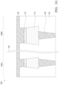
- the upper conductive layer 122 is used as a topmost layer of the conductive line structure in a first implementation of the subsequently formed resistive random access memory (such as the resistive random access memory 200 ), and the upper conductive layer 122 is used as a lower electrode of the memory unit in a second implementation of the subsequently formed resistive random access memory (such as the resistive random access memory 300 ).
- FIGS. 2 A and 2 B illustrate cross-sectional views of the resistive random access memory in a manufacturing process following FIG. 1 H , in accordance with the first implementation of the present disclosure.
- a lower electrode layer 124 , a metal oxide layer 126 , and an upper electrode 128 are sequentially formed over the upper conductive layer 122 and the dielectric layer 103 , and the lower electrode layer 124 is formed directly on an upper surface of the upper conductive layer 122 .
- the material of the lower electrode layer 124 and the upper electrode layer 128 may include platinum, titanium nitride, gold, titanium, tantalum, tantalum nitride, tungsten, tungsten nitride, copper, other suitable materials, or a combination thereof, and the lower electrode layer 124 and the upper electrode layer 128 may each include a single-layered structure or a multi-layered structure.
- the material of the metal oxide layer 126 may include a transition metal oxide, such as nickel oxide, titanium oxide, hafnium oxide, zirconium oxide, zinc oxide, tungsten oxide, aluminum oxide, tantalum oxide, molybdenum oxide, copper oxide, other suitable materials, or a combination thereof.
- a patterning process is performed to remove the lower electrode layer 124 , the metal oxide layer 126 , and the upper electrode layer 128 in a periphery circuit area 200 B, thereby forming a lower electrode 224 , a resistive switching layer 226 , and an upper electrode 228 in an array area 200 A, respectively.
- the resulted resistive random access memory 200 includes a conductive line structure 210 and a memory unit 220 , wherein the upper surface of the conductive line structure 210 is in direct contact with the lower electrode 224 of the memory unit 220 .
- via is not formed between the conductive line structure 210 and the memory unit 220 .
- the conductive line structure 210 includes the lower conductive layer 114 , the adhesion layer 116 , and the upper conductive layer 122
- the memory unit 220 includes the lower electrode 224 , the resistive switching layer 226 , and the upper electrode 228 in the array area 200 A.
- the lower electrode 224 , the resistive switching layer 226 , and the upper electrode 228 may have sidewalls that are substantially coplanar.
- the formation of other conductive structures is omitted between the conductive line structure 210 and the memory unit 220 , while reducing the contact resistance within the resistive random access memory 200 , it also simplifies the manufacturing process and reduces the cost.
- FIGS. 3 A and 3 B illustrate cross-sectional views of the resistive random access memory in a manufacturing process following FIG. 1 H , in accordance with the second implementation of the present disclosure.
- a metal oxide layer 126 and an upper electrode 128 are sequentially formed over the upper conductive layer 122 and the dielectric layer 103 , and the metal oxide layer 126 is formed directly on an upper surface of the upper conductive layer 122 .
- the material of the upper electrode layer 128 may include platinum, titanium nitride, gold, titanium, tantalum, tantalum nitride, tungsten, tungsten nitride, copper, other suitable materials, or a combination thereof, and the upper electrode layer 128 may include a single-layered structure or a multi-layered structure.
- the material of the metal oxide layer 126 may include a transition metal oxide, such as nickel oxide, titanium oxide, hafnium oxide, zirconium oxide, zinc oxide, tungsten oxide, aluminum oxide, tantalum oxide, molybdenum oxide, copper oxide, other suitable materials, or a combination thereof.
- a nitridation or oxidation treatment may be performed on the upper conductive layer 122 before forming the metal oxide layer 126 and the upper electrode layer. Therefore, the redox reaction to the metal oxide layer 126 (and the subsequently formed resistive switching layer 326 ) can be reduced to prevent the device from failing to undergo transition.
- a patterning process is performed to remove the metal oxide layer 126 and the upper electrode layer 128 in a periphery circuit area 300 B, thereby forming a resistive switching layer 326 , and an upper electrode 328 in an array area 300 A, respectively.
- sidewalls of the upper electrode 328 and the resistive switching layer 326 are substantially coplanar, and the widths of the upper electrode 328 and the resistive switching layer 326 are wider than the width of the upper conductive layer 122 .
- the resulted resistive random access memory 300 includes a conductive line structure 310 and a memory unit 320 , wherein the upper surface of the conductive line structure 310 is in direct contact with the upper conductive layer 122 of the memory unit 320 .
- the upper conductive layer 122 functions as a lower electrode of the memory unit 320 .
- via is not formed between the conductive line structure 310 and the memory unit 320 .
- the conductive line structure 310 of the array area 300 A includes the lower conductive layer 114 and the adhesion layer 116 , but does not include the upper conductive layer 122
- the conductive line structure 310 of the periphery circuit area 300 B includes the lower conductive layer 114 , the adhesion layer 116 , and the upper conductive layer 122
- the memory unit 320 includes the upper conductive layer 122 , the resistive switching layer 326 , and the upper electrode 328 in the array area 300 A, wherein the upper conductive layer 122 is used as a lower electrode of the memory unit 320 .
- a sidewall of the upper conductive layer 122 used as the lower electrode corresponds the sidewall of the conductive line structure 310 .
- the upper conductive layer 122 is buried in a trench in the dielectric layer 103 corresponding to the conductive line structure 310 , and the upper conductive layer 122 as the lower electrode may be formed directly on the upper surface of the adhesion layer 116 , so that the upper surface of the adhesion layer 116 is in direct contact with the upper conductive layer 122 . Since the upper conductive layer 122 is used as the lower electrode of the memory unit 320 directly, and the formation of other layers is omitted between the upper conductive layer 122 and the resistive switching layer 326 , while further reducing the contact resistance within the resistive random access memory 300 , it also simplifies the manufacturing process and reduces the cost.
- the resistive random access memories 200 and 300 convert their resistance value in the aforementioned manner to store or read data to achieve the memory function.
- the present disclosure provides a resistive random access memory an a method for manufacturing the same, wherein a conductive line structure is in contact with a memory unit directly, thereby reducing the series resistance within the resistive random access memory.
- a conductive line structure is in contact with a memory unit directly, thereby reducing the series resistance within the resistive random access memory.
Landscapes
- Engineering & Computer Science (AREA)
- Manufacturing & Machinery (AREA)
- Semiconductor Memories (AREA)
Abstract
Description
Claims (9)
Priority Applications (2)
| Application Number | Priority Date | Filing Date | Title |
|---|---|---|---|
| US17/571,149 US12336443B2 (en) | 2022-01-07 | 2022-01-07 | Resistive random access memory and method for manufacturing the same |
| US19/196,030 US20250268112A1 (en) | 2022-01-07 | 2025-05-01 | Resistive random access memory |
Applications Claiming Priority (1)
| Application Number | Priority Date | Filing Date | Title |
|---|---|---|---|
| US17/571,149 US12336443B2 (en) | 2022-01-07 | 2022-01-07 | Resistive random access memory and method for manufacturing the same |
Related Child Applications (1)
| Application Number | Title | Priority Date | Filing Date |
|---|---|---|---|
| US19/196,030 Division US20250268112A1 (en) | 2022-01-07 | 2025-05-01 | Resistive random access memory |
Publications (2)
| Publication Number | Publication Date |
|---|---|
| US20230225228A1 US20230225228A1 (en) | 2023-07-13 |
| US12336443B2 true US12336443B2 (en) | 2025-06-17 |
Family
ID=87069368
Family Applications (2)
| Application Number | Title | Priority Date | Filing Date |
|---|---|---|---|
| US17/571,149 Active 2043-07-29 US12336443B2 (en) | 2022-01-07 | 2022-01-07 | Resistive random access memory and method for manufacturing the same |
| US19/196,030 Pending US20250268112A1 (en) | 2022-01-07 | 2025-05-01 | Resistive random access memory |
Family Applications After (1)
| Application Number | Title | Priority Date | Filing Date |
|---|---|---|---|
| US19/196,030 Pending US20250268112A1 (en) | 2022-01-07 | 2025-05-01 | Resistive random access memory |
Country Status (1)
| Country | Link |
|---|---|
| US (2) | US12336443B2 (en) |
Families Citing this family (1)
| Publication number | Priority date | Publication date | Assignee | Title |
|---|---|---|---|---|
| CN119767682B (en) * | 2024-12-17 | 2025-09-23 | 北京大学 | Semiconductor structure and manufacturing method thereof |
Citations (9)
| Publication number | Priority date | Publication date | Assignee | Title |
|---|---|---|---|---|
| US20160204343A1 (en) * | 2015-01-09 | 2016-07-14 | Micron Technology, Inc. | Structures incorporating and methods of forming metal lines including carbon |
| US20180061890A1 (en) * | 2015-04-06 | 2018-03-01 | Nec Corporation | Switching element, semiconductor device, and semiconductor device manufacturing method |
| US20190229264A1 (en) * | 2016-09-30 | 2019-07-25 | Intel Corporation | Conductive bridge random access memory (cbram) devices with low thermal conductivity electrolyte sublayer |
| US20200020847A1 (en) | 2018-07-11 | 2020-01-16 | Samsung Electronics Co., Ltd. | Magnetic memory device and method for manufacturing the same |
| US20200090944A1 (en) * | 2018-09-13 | 2020-03-19 | Samsung Electronics Co., Ltd. | Semiconductor devices |
| TWI713029B (en) | 2019-11-25 | 2020-12-11 | 華邦電子股份有限公司 | Resistive random access memory and manufacturing method thereof |
| TWI718256B (en) | 2016-03-18 | 2021-02-11 | 南韓商三星電子股份有限公司 | Semiconductor memory devices and methods of manufacturing the same |
| TWI732232B (en) | 2019-04-18 | 2021-07-01 | 南亞科技股份有限公司 | Memory device and fabrication method thereof |
| US20210305160A1 (en) * | 2020-03-24 | 2021-09-30 | International Business Machines Corporation | Multi-metal interconnects for semiconductor device structures |
-
2022
- 2022-01-07 US US17/571,149 patent/US12336443B2/en active Active
-
2025
- 2025-05-01 US US19/196,030 patent/US20250268112A1/en active Pending
Patent Citations (9)
| Publication number | Priority date | Publication date | Assignee | Title |
|---|---|---|---|---|
| US20160204343A1 (en) * | 2015-01-09 | 2016-07-14 | Micron Technology, Inc. | Structures incorporating and methods of forming metal lines including carbon |
| US20180061890A1 (en) * | 2015-04-06 | 2018-03-01 | Nec Corporation | Switching element, semiconductor device, and semiconductor device manufacturing method |
| TWI718256B (en) | 2016-03-18 | 2021-02-11 | 南韓商三星電子股份有限公司 | Semiconductor memory devices and methods of manufacturing the same |
| US20190229264A1 (en) * | 2016-09-30 | 2019-07-25 | Intel Corporation | Conductive bridge random access memory (cbram) devices with low thermal conductivity electrolyte sublayer |
| US20200020847A1 (en) | 2018-07-11 | 2020-01-16 | Samsung Electronics Co., Ltd. | Magnetic memory device and method for manufacturing the same |
| US20200090944A1 (en) * | 2018-09-13 | 2020-03-19 | Samsung Electronics Co., Ltd. | Semiconductor devices |
| TWI732232B (en) | 2019-04-18 | 2021-07-01 | 南亞科技股份有限公司 | Memory device and fabrication method thereof |
| TWI713029B (en) | 2019-11-25 | 2020-12-11 | 華邦電子股份有限公司 | Resistive random access memory and manufacturing method thereof |
| US20210305160A1 (en) * | 2020-03-24 | 2021-09-30 | International Business Machines Corporation | Multi-metal interconnects for semiconductor device structures |
Also Published As
| Publication number | Publication date |
|---|---|
| US20230225228A1 (en) | 2023-07-13 |
| US20250268112A1 (en) | 2025-08-21 |
Similar Documents
| Publication | Publication Date | Title |
|---|---|---|
| US11889705B2 (en) | Interconnect landing method for RRAM technology | |
| CN107046096B (en) | Semiconductor structure and manufacturing method thereof | |
| US10014469B2 (en) | Resistive random access memory and manufacturing method thereof | |
| US11018299B2 (en) | Memory cell having resistance variable film and method of making the same | |
| KR20190031806A (en) | Semiconductor device and method for manufacturing the same | |
| TWI709166B (en) | Resistive random access memory array and manufacturing method thereof | |
| KR100533971B1 (en) | Method of manufacturing capacitor for semiconductor device | |
| US9299927B2 (en) | Memory cell having resistance variable film and method of making the same | |
| TWI702744B (en) | Resistive random access memory structure and manufacturing method thereof | |
| US20250268112A1 (en) | Resistive random access memory | |
| CN113380947A (en) | Semiconductor integrated circuit device and method for manufacturing the same | |
| JP7617171B2 (en) | Resistive random access memory having a post-patterned memory film to provide improved endurance characteristics and method of forming same | |
| US12087619B2 (en) | Semiconductor device and method of fabricating the same | |
| TWI785921B (en) | Resistive random access memory and method for forming the same | |
| TW202431975A (en) | Resistive random access memory device and fabrication method thereof | |
| CN116456725A (en) | Variable resistance memory and manufacturing method thereof | |
| CN110473961B (en) | Resistive random access memory structure and manufacturing method thereof | |
| US11329226B2 (en) | Memory devices including step shape electrode and methods for forming the same | |
| KR100605231B1 (en) | ME capacitor formation method of semiconductor device | |
| CN121038286A (en) | Magnetoresistive random access memory and its formation method |
Legal Events
| Date | Code | Title | Description |
|---|---|---|---|
| FEPP | Fee payment procedure |
Free format text: ENTITY STATUS SET TO UNDISCOUNTED (ORIGINAL EVENT CODE: BIG.); ENTITY STATUS OF PATENT OWNER: LARGE ENTITY |
|
| STPP | Information on status: patent application and granting procedure in general |
Free format text: DOCKETED NEW CASE - READY FOR EXAMINATION |
|
| AS | Assignment |
Owner name: WINBOND ELECTRONICS CORP., TAIWAN Free format text: ASSIGNMENT OF ASSIGNORS INTEREST;ASSIGNORS:LIU, CHI-CHING;HUANG, CHIH-CHAO;TSAI, SHIH-NING;REEL/FRAME:058968/0093 Effective date: 20210104 |
|
| STPP | Information on status: patent application and granting procedure in general |
Free format text: NON FINAL ACTION MAILED |
|
| STPP | Information on status: patent application and granting procedure in general |
Free format text: RESPONSE TO NON-FINAL OFFICE ACTION ENTERED AND FORWARDED TO EXAMINER |
|
| STPP | Information on status: patent application and granting procedure in general |
Free format text: FINAL REJECTION MAILED |
|
| STPP | Information on status: patent application and granting procedure in general |
Free format text: ADVISORY ACTION MAILED |
|
| STPP | Information on status: patent application and granting procedure in general |
Free format text: NOTICE OF ALLOWANCE MAILED -- APPLICATION RECEIVED IN OFFICE OF PUBLICATIONS |
|
| STCF | Information on status: patent grant |
Free format text: PATENTED CASE |