US12332565B2 - Thermosetting iodine- and silicon-containing material, composition containing the material for forming resist underlayer film for EUV lithography, and patterning process - Google Patents
Thermosetting iodine- and silicon-containing material, composition containing the material for forming resist underlayer film for EUV lithography, and patterning process Download PDFInfo
- Publication number
- US12332565B2 US12332565B2 US18/340,442 US202318340442A US12332565B2 US 12332565 B2 US12332565 B2 US 12332565B2 US 202318340442 A US202318340442 A US 202318340442A US 12332565 B2 US12332565 B2 US 12332565B2
- Authority
- US
- United States
- Prior art keywords
- group
- silicon
- film
- underlayer film
- resist underlayer
- Prior art date
- Legal status (The legal status is an assumption and is not a legal conclusion. Google has not performed a legal analysis and makes no representation as to the accuracy of the status listed.)
- Active
Links
Images


Classifications
-
- G—PHYSICS
- G03—PHOTOGRAPHY; CINEMATOGRAPHY; ANALOGOUS TECHNIQUES USING WAVES OTHER THAN OPTICAL WAVES; ELECTROGRAPHY; HOLOGRAPHY
- G03F—PHOTOMECHANICAL PRODUCTION OF TEXTURED OR PATTERNED SURFACES, e.g. FOR PRINTING, FOR PROCESSING OF SEMICONDUCTOR DEVICES; MATERIALS THEREFOR; ORIGINALS THEREFOR; APPARATUS SPECIALLY ADAPTED THEREFOR
- G03F7/00—Photomechanical, e.g. photolithographic, production of textured or patterned surfaces, e.g. printing surfaces; Materials therefor, e.g. comprising photoresists; Apparatus specially adapted therefor
- G03F7/004—Photosensitive materials
- G03F7/09—Photosensitive materials characterised by structural details, e.g. supports, auxiliary layers
- G03F7/094—Multilayer resist systems, e.g. planarising layers
-
- C—CHEMISTRY; METALLURGY
- C07—ORGANIC CHEMISTRY
- C07F—ACYCLIC, CARBOCYCLIC OR HETEROCYCLIC COMPOUNDS CONTAINING ELEMENTS OTHER THAN CARBON, HYDROGEN, HALOGEN, OXYGEN, NITROGEN, SULFUR, SELENIUM OR TELLURIUM
- C07F7/00—Compounds containing elements of Groups 4 or 14 of the Periodic Table
- C07F7/02—Silicon compounds
- C07F7/08—Compounds having one or more C—Si linkages
- C07F7/18—Compounds having one or more C—Si linkages as well as one or more C—O—Si linkages
- C07F7/1804—Compounds having Si-O-C linkages
-
- C—CHEMISTRY; METALLURGY
- C08—ORGANIC MACROMOLECULAR COMPOUNDS; THEIR PREPARATION OR CHEMICAL WORKING-UP; COMPOSITIONS BASED THEREON
- C08G—MACROMOLECULAR COMPOUNDS OBTAINED OTHERWISE THAN BY REACTIONS ONLY INVOLVING UNSATURATED CARBON-TO-CARBON BONDS
- C08G77/00—Macromolecular compounds obtained by reactions forming a linkage containing silicon with or without sulfur, nitrogen, oxygen or carbon in the main chain of the macromolecule
- C08G77/04—Polysiloxanes
- C08G77/14—Polysiloxanes containing silicon bound to oxygen-containing groups
- C08G77/18—Polysiloxanes containing silicon bound to oxygen-containing groups to alkoxy or aryloxy groups
-
- C—CHEMISTRY; METALLURGY
- C08—ORGANIC MACROMOLECULAR COMPOUNDS; THEIR PREPARATION OR CHEMICAL WORKING-UP; COMPOSITIONS BASED THEREON
- C08G—MACROMOLECULAR COMPOUNDS OBTAINED OTHERWISE THAN BY REACTIONS ONLY INVOLVING UNSATURATED CARBON-TO-CARBON BONDS
- C08G77/00—Macromolecular compounds obtained by reactions forming a linkage containing silicon with or without sulfur, nitrogen, oxygen or carbon in the main chain of the macromolecule
- C08G77/04—Polysiloxanes
- C08G77/22—Polysiloxanes containing silicon bound to organic groups containing atoms other than carbon, hydrogen and oxygen
- C08G77/24—Polysiloxanes containing silicon bound to organic groups containing atoms other than carbon, hydrogen and oxygen halogen-containing groups
-
- G—PHYSICS
- G03—PHOTOGRAPHY; CINEMATOGRAPHY; ANALOGOUS TECHNIQUES USING WAVES OTHER THAN OPTICAL WAVES; ELECTROGRAPHY; HOLOGRAPHY
- G03F—PHOTOMECHANICAL PRODUCTION OF TEXTURED OR PATTERNED SURFACES, e.g. FOR PRINTING, FOR PROCESSING OF SEMICONDUCTOR DEVICES; MATERIALS THEREFOR; ORIGINALS THEREFOR; APPARATUS SPECIALLY ADAPTED THEREFOR
- G03F7/00—Photomechanical, e.g. photolithographic, production of textured or patterned surfaces, e.g. printing surfaces; Materials therefor, e.g. comprising photoresists; Apparatus specially adapted therefor
- G03F7/0035—Multiple processes, e.g. applying a further resist layer on an already in a previously step, processed pattern or textured surface
-
- G—PHYSICS
- G03—PHOTOGRAPHY; CINEMATOGRAPHY; ANALOGOUS TECHNIQUES USING WAVES OTHER THAN OPTICAL WAVES; ELECTROGRAPHY; HOLOGRAPHY
- G03F—PHOTOMECHANICAL PRODUCTION OF TEXTURED OR PATTERNED SURFACES, e.g. FOR PRINTING, FOR PROCESSING OF SEMICONDUCTOR DEVICES; MATERIALS THEREFOR; ORIGINALS THEREFOR; APPARATUS SPECIALLY ADAPTED THEREFOR
- G03F7/00—Photomechanical, e.g. photolithographic, production of textured or patterned surfaces, e.g. printing surfaces; Materials therefor, e.g. comprising photoresists; Apparatus specially adapted therefor
- G03F7/004—Photosensitive materials
- G03F7/0046—Photosensitive materials with perfluoro compounds, e.g. for dry lithography
-
- G—PHYSICS
- G03—PHOTOGRAPHY; CINEMATOGRAPHY; ANALOGOUS TECHNIQUES USING WAVES OTHER THAN OPTICAL WAVES; ELECTROGRAPHY; HOLOGRAPHY
- G03F—PHOTOMECHANICAL PRODUCTION OF TEXTURED OR PATTERNED SURFACES, e.g. FOR PRINTING, FOR PROCESSING OF SEMICONDUCTOR DEVICES; MATERIALS THEREFOR; ORIGINALS THEREFOR; APPARATUS SPECIALLY ADAPTED THEREFOR
- G03F7/00—Photomechanical, e.g. photolithographic, production of textured or patterned surfaces, e.g. printing surfaces; Materials therefor, e.g. comprising photoresists; Apparatus specially adapted therefor
- G03F7/004—Photosensitive materials
- G03F7/06—Silver salts
- G03F7/063—Additives or means to improve the lithographic properties; Processing solutions characterised by such additives; Treatment after development or transfer, e.g. finishing, washing; Correction or deletion fluids
- G03F7/066—Organic derivatives of bivalent sulfur, e.g. onium derivatives
-
- G—PHYSICS
- G03—PHOTOGRAPHY; CINEMATOGRAPHY; ANALOGOUS TECHNIQUES USING WAVES OTHER THAN OPTICAL WAVES; ELECTROGRAPHY; HOLOGRAPHY
- G03F—PHOTOMECHANICAL PRODUCTION OF TEXTURED OR PATTERNED SURFACES, e.g. FOR PRINTING, FOR PROCESSING OF SEMICONDUCTOR DEVICES; MATERIALS THEREFOR; ORIGINALS THEREFOR; APPARATUS SPECIALLY ADAPTED THEREFOR
- G03F7/00—Photomechanical, e.g. photolithographic, production of textured or patterned surfaces, e.g. printing surfaces; Materials therefor, e.g. comprising photoresists; Apparatus specially adapted therefor
- G03F7/004—Photosensitive materials
- G03F7/075—Silicon-containing compounds
- G03F7/0751—Silicon-containing compounds used as adhesion-promoting additives or as means to improve adhesion
-
- G—PHYSICS
- G03—PHOTOGRAPHY; CINEMATOGRAPHY; ANALOGOUS TECHNIQUES USING WAVES OTHER THAN OPTICAL WAVES; ELECTROGRAPHY; HOLOGRAPHY
- G03F—PHOTOMECHANICAL PRODUCTION OF TEXTURED OR PATTERNED SURFACES, e.g. FOR PRINTING, FOR PROCESSING OF SEMICONDUCTOR DEVICES; MATERIALS THEREFOR; ORIGINALS THEREFOR; APPARATUS SPECIALLY ADAPTED THEREFOR
- G03F7/00—Photomechanical, e.g. photolithographic, production of textured or patterned surfaces, e.g. printing surfaces; Materials therefor, e.g. comprising photoresists; Apparatus specially adapted therefor
- G03F7/004—Photosensitive materials
- G03F7/075—Silicon-containing compounds
- G03F7/0752—Silicon-containing compounds in non photosensitive layers or as additives, e.g. for dry lithography
-
- G—PHYSICS
- G03—PHOTOGRAPHY; CINEMATOGRAPHY; ANALOGOUS TECHNIQUES USING WAVES OTHER THAN OPTICAL WAVES; ELECTROGRAPHY; HOLOGRAPHY
- G03F—PHOTOMECHANICAL PRODUCTION OF TEXTURED OR PATTERNED SURFACES, e.g. FOR PRINTING, FOR PROCESSING OF SEMICONDUCTOR DEVICES; MATERIALS THEREFOR; ORIGINALS THEREFOR; APPARATUS SPECIALLY ADAPTED THEREFOR
- G03F7/00—Photomechanical, e.g. photolithographic, production of textured or patterned surfaces, e.g. printing surfaces; Materials therefor, e.g. comprising photoresists; Apparatus specially adapted therefor
- G03F7/004—Photosensitive materials
- G03F7/075—Silicon-containing compounds
- G03F7/0757—Macromolecular compounds containing Si-O, Si-C or Si-N bonds
-
- G—PHYSICS
- G03—PHOTOGRAPHY; CINEMATOGRAPHY; ANALOGOUS TECHNIQUES USING WAVES OTHER THAN OPTICAL WAVES; ELECTROGRAPHY; HOLOGRAPHY
- G03F—PHOTOMECHANICAL PRODUCTION OF TEXTURED OR PATTERNED SURFACES, e.g. FOR PRINTING, FOR PROCESSING OF SEMICONDUCTOR DEVICES; MATERIALS THEREFOR; ORIGINALS THEREFOR; APPARATUS SPECIALLY ADAPTED THEREFOR
- G03F7/00—Photomechanical, e.g. photolithographic, production of textured or patterned surfaces, e.g. printing surfaces; Materials therefor, e.g. comprising photoresists; Apparatus specially adapted therefor
- G03F7/004—Photosensitive materials
- G03F7/09—Photosensitive materials characterised by structural details, e.g. supports, auxiliary layers
- G03F7/091—Photosensitive materials characterised by structural details, e.g. supports, auxiliary layers characterised by antireflection means or light filtering or absorbing means, e.g. anti-halation, contrast enhancement
-
- G—PHYSICS
- G03—PHOTOGRAPHY; CINEMATOGRAPHY; ANALOGOUS TECHNIQUES USING WAVES OTHER THAN OPTICAL WAVES; ELECTROGRAPHY; HOLOGRAPHY
- G03F—PHOTOMECHANICAL PRODUCTION OF TEXTURED OR PATTERNED SURFACES, e.g. FOR PRINTING, FOR PROCESSING OF SEMICONDUCTOR DEVICES; MATERIALS THEREFOR; ORIGINALS THEREFOR; APPARATUS SPECIALLY ADAPTED THEREFOR
- G03F7/00—Photomechanical, e.g. photolithographic, production of textured or patterned surfaces, e.g. printing surfaces; Materials therefor, e.g. comprising photoresists; Apparatus specially adapted therefor
- G03F7/004—Photosensitive materials
- G03F7/09—Photosensitive materials characterised by structural details, e.g. supports, auxiliary layers
- G03F7/11—Photosensitive materials characterised by structural details, e.g. supports, auxiliary layers having cover layers or intermediate layers, e.g. subbing layers
-
- G—PHYSICS
- G03—PHOTOGRAPHY; CINEMATOGRAPHY; ANALOGOUS TECHNIQUES USING WAVES OTHER THAN OPTICAL WAVES; ELECTROGRAPHY; HOLOGRAPHY
- G03F—PHOTOMECHANICAL PRODUCTION OF TEXTURED OR PATTERNED SURFACES, e.g. FOR PRINTING, FOR PROCESSING OF SEMICONDUCTOR DEVICES; MATERIALS THEREFOR; ORIGINALS THEREFOR; APPARATUS SPECIALLY ADAPTED THEREFOR
- G03F7/00—Photomechanical, e.g. photolithographic, production of textured or patterned surfaces, e.g. printing surfaces; Materials therefor, e.g. comprising photoresists; Apparatus specially adapted therefor
- G03F7/20—Exposure; Apparatus therefor
- G03F7/2002—Exposure; Apparatus therefor with visible light or UV light, through an original having an opaque pattern on a transparent support, e.g. film printing, projection printing; by reflection of visible or UV light from an original such as a printed image
- G03F7/2004—Exposure; Apparatus therefor with visible light or UV light, through an original having an opaque pattern on a transparent support, e.g. film printing, projection printing; by reflection of visible or UV light from an original such as a printed image characterised by the use of a particular light source, e.g. fluorescent lamps or deep UV light
-
- G—PHYSICS
- G03—PHOTOGRAPHY; CINEMATOGRAPHY; ANALOGOUS TECHNIQUES USING WAVES OTHER THAN OPTICAL WAVES; ELECTROGRAPHY; HOLOGRAPHY
- G03F—PHOTOMECHANICAL PRODUCTION OF TEXTURED OR PATTERNED SURFACES, e.g. FOR PRINTING, FOR PROCESSING OF SEMICONDUCTOR DEVICES; MATERIALS THEREFOR; ORIGINALS THEREFOR; APPARATUS SPECIALLY ADAPTED THEREFOR
- G03F7/00—Photomechanical, e.g. photolithographic, production of textured or patterned surfaces, e.g. printing surfaces; Materials therefor, e.g. comprising photoresists; Apparatus specially adapted therefor
- G03F7/20—Exposure; Apparatus therefor
- G03F7/2002—Exposure; Apparatus therefor with visible light or UV light, through an original having an opaque pattern on a transparent support, e.g. film printing, projection printing; by reflection of visible or UV light from an original such as a printed image
- G03F7/2012—Exposure; Apparatus therefor with visible light or UV light, through an original having an opaque pattern on a transparent support, e.g. film printing, projection printing; by reflection of visible or UV light from an original such as a printed image using liquid photohardening compositions, e.g. for the production of reliefs such as flexographic plates or stamps
-
- G—PHYSICS
- G03—PHOTOGRAPHY; CINEMATOGRAPHY; ANALOGOUS TECHNIQUES USING WAVES OTHER THAN OPTICAL WAVES; ELECTROGRAPHY; HOLOGRAPHY
- G03F—PHOTOMECHANICAL PRODUCTION OF TEXTURED OR PATTERNED SURFACES, e.g. FOR PRINTING, FOR PROCESSING OF SEMICONDUCTOR DEVICES; MATERIALS THEREFOR; ORIGINALS THEREFOR; APPARATUS SPECIALLY ADAPTED THEREFOR
- G03F7/00—Photomechanical, e.g. photolithographic, production of textured or patterned surfaces, e.g. printing surfaces; Materials therefor, e.g. comprising photoresists; Apparatus specially adapted therefor
- G03F7/26—Processing photosensitive materials; Apparatus therefor
- G03F7/36—Imagewise removal not covered by groups G03F7/30 - G03F7/34, e.g. using gas streams, using plasma
-
- G—PHYSICS
- G03—PHOTOGRAPHY; CINEMATOGRAPHY; ANALOGOUS TECHNIQUES USING WAVES OTHER THAN OPTICAL WAVES; ELECTROGRAPHY; HOLOGRAPHY
- G03F—PHOTOMECHANICAL PRODUCTION OF TEXTURED OR PATTERNED SURFACES, e.g. FOR PRINTING, FOR PROCESSING OF SEMICONDUCTOR DEVICES; MATERIALS THEREFOR; ORIGINALS THEREFOR; APPARATUS SPECIALLY ADAPTED THEREFOR
- G03F7/00—Photomechanical, e.g. photolithographic, production of textured or patterned surfaces, e.g. printing surfaces; Materials therefor, e.g. comprising photoresists; Apparatus specially adapted therefor
- G03F7/70—Microphotolithographic exposure; Apparatus therefor
- G03F7/70008—Production of exposure light, i.e. light sources
- G03F7/70033—Production of exposure light, i.e. light sources by plasma extreme ultraviolet [EUV] sources
-
- H—ELECTRICITY
- H10—SEMICONDUCTOR DEVICES; ELECTRIC SOLID-STATE DEVICES NOT OTHERWISE PROVIDED FOR
- H10P—GENERIC PROCESSES OR APPARATUS FOR THE MANUFACTURE OR TREATMENT OF DEVICES COVERED BY CLASS H10
- H10P14/00—Formation of materials, e.g. in the shape of layers or pillars
- H10P14/60—Formation of materials, e.g. in the shape of layers or pillars of insulating materials
- H10P14/63—Formation of materials, e.g. in the shape of layers or pillars of insulating materials characterised by the formation processes
- H10P14/6326—Deposition processes
- H10P14/6328—Deposition from the gas or vapour phase
- H10P14/6334—Deposition from the gas or vapour phase using decomposition or reaction of gaseous or vapour phase compounds, i.e. chemical vapour deposition
-
- H—ELECTRICITY
- H10—SEMICONDUCTOR DEVICES; ELECTRIC SOLID-STATE DEVICES NOT OTHERWISE PROVIDED FOR
- H10P—GENERIC PROCESSES OR APPARATUS FOR THE MANUFACTURE OR TREATMENT OF DEVICES COVERED BY CLASS H10
- H10P14/00—Formation of materials, e.g. in the shape of layers or pillars
- H10P14/60—Formation of materials, e.g. in the shape of layers or pillars of insulating materials
- H10P14/69—Inorganic materials
- H10P14/692—Inorganic materials composed of oxides, glassy oxides or oxide-based glasses
- H10P14/6938—Inorganic materials composed of oxides, glassy oxides or oxide-based glasses the material containing at least one metal element, e.g. metal oxides, metal oxynitrides or metal oxycarbides
-
- H—ELECTRICITY
- H10—SEMICONDUCTOR DEVICES; ELECTRIC SOLID-STATE DEVICES NOT OTHERWISE PROVIDED FOR
- H10P—GENERIC PROCESSES OR APPARATUS FOR THE MANUFACTURE OR TREATMENT OF DEVICES COVERED BY CLASS H10
- H10P76/00—Manufacture or treatment of masks on semiconductor bodies, e.g. by lithography or photolithography
Definitions
- the present invention relates to a thermosetting iodine- and silicon-containing material, a composition containing this material for forming a resist underlayer film for EUV lithography, and a patterning process.
- EUV extreme ultraviolet
- ArF ArF excimer laser
- An object of the present invention is to provide: a thermosetting silicon-containing material used for forming a resist underlayer film which is capable of contributing to sensitivity enhancement of an upper layer resist while keeping LWR thereof from degrading; a composition for forming a silicon-containing resist underlayer film, the composition containing the thermosetting silicon-containing material; and a patterning process using this composition.
- thermosetting silicon-containing material comprising one or more of
- R 1 represents an iodine-containing organic group
- R 2 and R 3 are each independently identical to R 1 , a hydrogen atom, or a monovalent organic group having 1 to 30 carbon atoms.
- thermosetting silicon-containing material makes it possible to obtain a composition for forming a resist underlayer film which is capable of contributing to sensitivity enhancement of an upper layer resist while keeping LWR thereof from degrading.
- the R 1 is preferably shown by the following general formula (Sx-R1):
- R 11 represents a single bond or a divalent organic group
- R 12 represents a monovalent organic group having 1 to 10 carbon atoms, a hydroxyl group, or a halogen atom other than iodine
- n1 is 1, 2, or 3
- n2 is 0, 1, or 2.
- thermosetting silicon-containing material can make a composition for forming a resist underlayer film which is capable of contributing to further sensitivity enhancement of an upper layer resist while keeping LWR thereof from degrading.
- composition for forming a silicon-containing resist underlayer film for EUV lithography comprising:
- Such a composition for forming a silicon-containing resist underlayer film in EUV lithography can form a resist underlayer film which is capable of contributing to sensitivity enhancement of an upper layer resist while keeping LWR thereof from degrading.
- the crosslinking catalyst may be a sulfonium salt, an iodonium salt, a phosphonium salt, an ammonium salt, a polysiloxane having a structure containing one of these salts as a part, or an alkaline metal salt.
- Such a crosslinking catalyst in combination with the inventive thermosetting silicon-containing material makes it possible to obtain a resist underlayer film which is capable of contributing to further sensitivity enhancement of an upper layer resist while keeping LWR thereof from degrading.
- the inventive composition for forming a silicon-containing resist underlayer film for EUV lithography may further comprise at least one compound shown by the following general formula (P-0):
- R 300 represents a divalent organic group substituted with one or more fluorine atoms
- R 301 and R 302 each independently represent a linear, branched, or cyclic monovalent hydrocarbon group having 1 to 20 carbon atoms optionally substituted with a hetero atom or optionally containing a hetero atom
- R 303 represents a linear, branched, or cyclic divalent hydrocarbon group having 1 to 20 carbon atoms optionally substituted with a hetero atom or optionally containing a hetero atom
- R 301 and R 302 , or R 301 and R 303 are optionally bonded to each other to form a ring with a sulfur atom in the formula
- L 304 represents a single bond or a linear, branched, or cyclic divalent hydrocarbon group having 1 to 20 carbon atoms optionally substituted with a hetero atom or optionally containing a hetero atom.
- Such a compound (acid generator) in combination with the inventive thermosetting silicon-containing material can make a resist underlayer film which is capable of contributing to the formation of an upper layer resist having a rectangular cross section while keeping the LWR of the upper layer resist from degrading.
- the compound shown by the general formula (P-0) is preferably a compound shown by the following general formula (P-1):
- X 305 and X 306 each independently represent a hydrogen atom, a fluorine atom, or a trifluoromethyl group, but both are not hydrogen atoms simultaneously; n307 represents an integer of 1 to 4; and R 301 , R 302 , R 303 , and L 304 are as defined above.
- the present invention provides a patterning process comprising:
- the pattern formed in the photoresist can be formed onto the substrate without changing the size during the transfer.
- the present invention provides a patterning process comprising:
- the pattern formed in the photoresist can be formed onto the substrate without changing the size during the transfer.
- the body to be processed may be a semiconductor device substrate, a metal film, an alloy film, a metal carbide film, a metal oxide film, a metal nitride film, a metal oxycarbide film, or a metal oxynitride film.
- the organic underlayer film or CVD film is formed on the body to be processed, so that the pattern can be formed onto the substrate (film) precisely without changing the size during the transfer.
- the metal of the body to be processed may be silicon, gallium, titanium, tungsten, hafnium, zirconium, chromium, germanium, copper, aluminum, cobalt, iron, or an alloy thereof.
- the body to be processed is etched precisely, so that a positive pattern can be transferred with high precision to the body to be processed.
- a resist underlayer film having an iodine atom-substituted aromatic ring has the following characteristics. Since the resist underlayer film contains iodine atoms capable of showing high light absorption, secondary electrons generated from the iodine atoms produce a sensitization effect during light exposure. Further, an iodine atom has such a large atomic weight that the iodine produces a high effect of suppressing the acid diffusion from an upper layer resist into the resist underlayer film.
- the resist underlayer film is capable of increasing the sensitivity of the resist upper layer film while keeping the intrinsic LWR property of the resist upper layer film.
- this resist underlayer film has high etching selectivity relative to an organic material, so that a photoresist pattern formed in the resist underlayer film can be successively transferred from the silicon-containing resist underlayer film to an organic underlayer film or CVD organic hard mask by dry etching process.
- a photoresist film tends to be formed thinner to prevent pattern collapse after development, thereby making it difficult to transfer a pattern to a resist underlayer film.
- the use of the inventive composition for forming a silicon-containing resist underlayer film makes it possible to suppress deformation of a photoresist pattern during dry etching and transfer this pattern to a substrate with high precision, even when a thin photoresist film is used as an etching mask.
- FIG. 1 is a flow diagram showing a patterning process of the present invention.
- thermosetting silicon-containing material used for forming a resist underlayer film which can contribute to sensitivity enhancement of an upper layer resist while keeping LWR thereof from degrading
- a composition for forming a silicon-containing resist underlayer film, the composition containing the thermosetting silicon-containing material and a patterning process using the composition.
- the present inventors have earnestly studied to achieve the above object and consequently found that the sensitivity of an upper layer resist can be improved without degrading the LWR thereof by introducing iodine atoms into a silicon-containing resist underlayer film. Thus, the present invention has been completed.
- thermosetting silicon-containing material comprising one or more of
- R 1 represents an iodine-containing organic group
- R 2 and R 3 are each independently identical to R 1 , a hydrogen atom, or a monovalent organic group having 1 to 30 carbon atoms.
- the inventive thermosetting silicon-containing material (Sx) contains one or more of a repeating unit shown by the general formula (Sx-1), a repeating unit shown by the general formula (Sx-2), and a partial structure shown by the general formula (Sx-3).
- R 1 is an iodine-containing organic group.
- organic group means a group containing carbon which may further contain hydrogen and also nitrogen, oxygen, sulfur, silicon, a halogen atom, or the like (the same applies hereinafter).
- R 1 is not particularly limited as long as it is an iodine-containing organic group, and is preferably an organic group in which at least one hydrogen atom of an aromatic ring of an aryl group or an aralkyl group is substituted with an iodine atom.
- thermosetting silicon-containing material having such an iodine atom-substituted aromatic ring has the following characteristics. Specifically, since the thermosetting silicon-containing material contains iodine atoms capable of absorbing light greatly, when the thermosetting silicon-containing material is used to form a resist underlayer film, a sensitization effect is produced because of secondary electrons generated from the iodine atoms during exposure. Further, since an iodine atom has a large atomic weight, iodine has a high effect of suppressing the acid diffusion from an upper layer resist into the resist underlayer film. Moreover, the thermosetting silicon-containing material is capable of increasing the sensitivity of the resist upper layer film while keeping the LWR property the resist upper layer film intrinsically has.
- R 1 having an iodine atom-substituted aromatic ring is preferably shown by the following general formula (Sx-R1):
- R 11 represents a single bond or a divalent organic group
- R 12 represents a monovalent organic group having 1 to 10 carbon atoms, a hydroxyl group, or a halogen atom other than iodine
- n1 is 1, 2, or 3
- n2 is 0, 1, or 2.
- R 11 is a divalent organic group
- the divalent organic group is not particularly limited, but examples thereof include substituted or unsubstituted alkylene groups, substituted or unsubstituted alkenylene groups, substituted or unsubstituted arylene groups, substituted or unsubstituted aralkylene groups, —O—, —NH—, —CO—, —OCO—, —COO—, —OCOO—, and combinations thereof.
- R 11 include a single bond, a methylene group, an ethylene group, a carbonyloxymethylene group, a carbonyloxyethylene group, a carbonyloxypropylene group, an oxymethylene group, an oxyethylene group, and an oxypropylene group.
- R 12 is a monovalent organic group having 1 to 10 carbon atoms, a hydroxyl group, or a halogen atom other than iodine.
- R 12 include a methyl group, an ethyl group, a propyl group, a butyl group, a pentyl group, a hexyl group, a heptyl group, an octyl group, a nonyl group, a decyl group, a cyclopentyl group, a cyclohexyl group, a cycloheptyl group, a cyclopentylmethyl group, a cyclohexylmethyl group, a 4-methylcyclohexyl group, a vinyl group, an allyl group, a phenyl group, an ethynyl group, a methoxy group, an ethoxy group, a propoxy group, a butoxy group, a pentyloxy group
- R 2 and R 3 are each independently identical to R 1 , or a hydrogen atom or a monovalent organic group having 1 to 30 carbon atoms.
- Examples of the organic group (Sx-R1) having an iodine atom-substituted aromatic ring shown as R 1 in the inventive iodine-containing, thermosetting silicon-containing materials (Sx-1), (Sx-2), and (Sx-3) include ones having structures shown by the following formulae. Note that, in the following formulae, (Si) is depicted to show a bonding site to Si.
- an iodine-containing hydrolysable monomer used as a raw material for forming the inventive structures it is possible to use a monomer having one of the foregoing structures on a silicon atom and also containing, as a hydrolysable group(s): one, two, or three among chlorine, bromine, iodine, an acetoxy group, a methoxy group, an ethoxy group, a propoxy group, a butoxy group, and so forth; and if any, as R 2 or R 3 , one or a combination of two or more among a hydrogen atom and monovalent organic groups having 1 to 30 carbon atoms.
- An example of such an iodine-containing hydrolysable monomer includes a compound shown by the following general formula (Sm-I).
- Y represents a hydrolysable group selected from chlorine, bromine, iodine, an acetoxy group, a methoxy group, an ethoxy group, a propoxy group, and a butoxy group;
- a represents an integer of 1 to 3, and ⁇ , and ⁇ each represent 0 or 1, provided that 1 ⁇ ( ⁇ + ⁇ + ⁇ ) ⁇ 3.
- the inventive thermosetting silicon-containing material (Sx) can be produced by hydrolysis condensation of the iodine-containing hydrolysable monomer (Sm-I).
- the inventive silicon-containing material (Sx) can also be produced by hydrolysis condensation of a mixture containing this iodine-containing hydrolysable monomer and the following hydrolysable monomer (Sm).
- hydrolysable monomer (Sm) examples include tetramethoxysilane, tetraethoxysilane, tetrapropoxysilane, tetraisopropoxysilane, trimethoxysilane, triethoxysilane, tripropoxysilane, triisopropoxysilane, methyltrimethoxysilane, methyltriethoxysilane, methyltripropoxysilane, methyltriisopropoxysilane, ethyltrimethoxysilane, ethyltriethoxysilane, ethyltripropoxysilane, ethyltriisopropoxysilane, vinyltrimethoxysilane, vinyltriethoxysilane, vinyltripropoxysilane, vinyltriisopropoxysilane, propyltrimethoxysilane, propyltriethoxysilane, propyltripropoxysilane, propyltriiso
- the monomer Sm include tetramethoxysilane, tetraethoxysilane, methyltrimethoxysilane, methyltriethoxysilane, ethyltrimethoxysilane, ethyltriethoxysilane, vinyltrimethoxysilane, vinyltriethoxysilane, propyltrimethoxysilane, propyltriethoxysilane, isopropyltrimethoxysilane, isopropyltriethoxysilane, butyltrimethoxysilane, butyltriethoxysilane, isobutyltrimethoxysilane, isobutyltriethoxysilane, allyltrimethoxysilane, allyltriethoxysilane, cyclopentyltrimethoxysilane, cyclopentyltriethoxysilane, cyclohexyltrimethoxys
- organic group shown by R 2 and R 3 include organic groups having one or more carbon-oxygen single bonds or carbon-oxygen double bonds, specifically organic groups having one or more groups selected from the group consisting of cyclic ether groups, ester groups, alkoxy groups, and a hydroxy group.
- organic groups include ones shown by the following general formula (Sm-R).
- P represents a hydrogen atom, a cyclic ether group, a hydroxyl group, an alkoxy group having 1 to 4 carbon atoms, an alkylcarbonyloxy group having 1 to 6 carbon atoms, or an alkylcarbonyl group having 1 to 6 carbon atoms;
- u represents an integer of 0 to 3;
- S 1 and S 2 each independently represent —O—, —CO—, —OCO—, —
- T examples of the alicyclic, aromatic, or heterocyclic ring optionally containing a hetero atom such as an oxygen atom are shown below.
- positions bonded to Q 2 and Q 3 are not particularly limited, and can be selected appropriately in consideration of reactivity dependent on steric factors, availability of commercial reagents used in the reaction, and so on.
- organic groups having one or more carbon-oxygen single bonds or carbon-oxygen double bonds in the general formula (Sm-R) include the following. Note that, in the following formulae, (Si) is depicted to show a bonding site to Si.
- an organic group containing a silicon-silicon bond can also be used. Specific examples thereof include the following.
- an organic group having a protective group that is decomposed with an acid can also be used.
- an organic group having a fluorine atom can also be used.
- organic groups obtained from silicon compounds shown from paragraphs (0059) to (0065) of Japanese Unexamined Patent Application Publication No. 2012-53253 include organic groups obtained from silicon compounds shown from paragraphs (0059) to (0065) of Japanese Unexamined Patent Application Publication No. 2012-53253.
- an organic group having a nitrogen atom and a sulfur atom can also be used.
- the inventive silicon-containing material (Sx) can be produced, for example, by hydrolysis condensation of the above-described iodine-containing monomer (Sm-I) or a mixture of (Sm-I) with one or more of the hydrolysable monomers (Sm) (hereinafter, such a mixture will be collectively referred to as monomer) in the presence of an acid catalyst.
- Examples of the acid catalyst used in this event include organic acids such as formic acid, acetic acid, oxalic acid, maleic acid, methanesulfonic acid, benzenesulfonic acid, and toluenesulfonic acid; inorganic acids such as hydrofluoric acid, hydrochloric acid, hydrobromic acid, sulfuric acid, nitric acid, perchloric acid, and phosphoric acid; and the like.
- the catalyst can be used in an amount of 1 ⁇ 10 ⁇ 6 to 10 mol, preferably 1 ⁇ 10 ⁇ 5 to 5 mol, more preferably 1 ⁇ 10 ⁇ 4 to 1 mol, relative to 1 mol of the monomer.
- water is preferably added in an amount of 0.01 to 100 mol, more preferably 0.05 to 50 mol, further preferably 0.1 to 30 mol, per mol of the hydrolysable substituent bonded to the monomer.
- the amount is 100 mol or less, a reaction device can be made small and economical.
- the monomer is added to a catalyst aqueous solution to start the hydrolysis condensation reaction.
- an organic solvent may be added to the catalyst aqueous solution, or the monomer may be diluted with an organic solvent, or both of these operations may be performed.
- the reaction temperature may be 0 to 100° C., preferably 5 to 80° C.
- the temperature is maintained at 5 to 80° C., and then the mixture is aged at 20 to 80° C.
- the organic solvent which can be added to the catalyst aqueous solution or with which the monomer can be diluted is preferably methanol, ethanol, 1-propanol, 2-propanol, 1-butanol, 2-butanol, 2-methyl-1-propanol, acetone, acetonitrile, tetrahydrofuran, toluene, hexane, ethyl acetate, methyl ethyl ketone, methyl isobutyl ketone, cyclohexanone, methyl amyl ketone, butanediol monomethyl ether, propylene glycol monomethyl ether, ethylene glycol monomethyl ether, butanediol monoethyl ether, propylene glycol monoethyl ether, ethylene glycol monoethyl ether, propylene glycol dimethyl ether, diethylene glycol dimethyl ether, propylene glycol monomethyl ether acetate, propylene
- water-soluble solvents are preferable.
- examples thereof include alcohols such as methanol, ethanol, 1-propanol, and 2-propanol; polyhydric alcohols such as ethylene glycol and propylene glycol; polyhydric alcohol condensate derivatives such as butanediol monomethyl ether, propylene glycol monomethyl ether, ethylene glycol monomethyl ether, butanediol monoethyl ether, propylene glycol monoethyl ether, ethylene glycol monoethyl ether, butanediol monopropyl ether, propylene glycol monopropyl ether, and ethylene glycol monopropyl ether; acetone, acetonitrile, tetrahydrofuran, and the like.
- particularly preferable is one having a boiling point of 100° C. or less.
- the organic solvent is used in an amount of preferably 0 to 1,000 ml, particularly preferably 0 to 500 ml, relative to 1 mol of the monomer.
- the organic solvent is used in a small amount, only a small reaction vessel is required and economical.
- the amount of an alkaline substance usable for the neutralization is preferably 0.1 to 2 equivalents relative to the acid used as the catalyst.
- This alkaline substance may be any substance as long as it shows alkalinity in water.
- by-products such as alcohol produced by the hydrolysis condensation reaction are desirably removed from the reaction mixture by a procedure such as removal under reduced pressure.
- the reaction mixture is heated at a temperature of preferably 0 to 100° C., more preferably 10 to 90° C., further preferably 15 to 80° C., although the temperature depends on the kinds of the added organic solvent, the alcohol produced in the reaction, and so forth.
- the degree of vacuum is preferably atmospheric pressure or less, more preferably 80 kPa or less in absolute pressure, further preferably 50 kPa or less in absolute pressure, although the degree of vacuum varies depending on the kinds of the organic solvent, alcohol, etc. to be removed, as well as exhausting equipment, condensation equipment, and heating temperature. In this case, it is difficult to accurately know the amount of alcohol to be removed, but it is desirable to remove about 80 mass % or more of the produced alcohol, etc.
- the acid catalyst used in the hydrolysis condensation may be removed from the reaction mixture.
- the silicon-containing material is mixed with water, and the silicon-containing material is extracted with an organic solvent.
- the organic solvent used in this event is capable of dissolving the silicon-containing material and achieves two-layer separation when mixed with water.
- organic solvent examples include methanol, ethanol, 1-propanol, 2-propanol, 1-butanol, 2-butanol, 2-methyl-1-propanol, acetone, tetrahydrofuran, toluene, hexane, ethyl acetate, cyclohexanone, methyl amyl ketone, butanediol monomethyl ether, propylene glycol monomethyl ether, ethylene glycol monomethyl ether, butanediol monoethyl ether, propylene glycol monoethyl ether, ethylene glycol monoethyl ether, butanediol monopropyl ether, propylene glycol monopropyl ether, ethylene glycol monopropyl ether, propylene glycol dimethyl ether, diethylene glycol dimethyl ether, propylene glycol monomethyl ether acetate, propylene glycol monoethyl ether acetate, eth
- a mixture of a water-soluble organic solvent and a slightly-water-soluble organic solvent Preferable examples of the mixture include methanol-ethyl acetate mixture, ethanol-ethyl acetate mixture, 1-propanol-ethyl acetate mixture, 2-propanol-ethyl acetate mixture, butanediol monomethyl ether-ethyl acetate mixture, propylene glycol monomethyl ether-ethyl acetate mixture, ethylene glycol monomethyl ether-ethyl acetate mixture, butanediol monoethyl ether-ethyl acetate mixture, propylene glycol monoethyl ether-ethyl acetate mixture, ethylene glycol monoethyl ether-ethyl acetate mixture, butanediol monopropyl ether-ethyl acetate mixture, propylene glycol monopropyl ether-ethyl acetate mixture, prop
- the amount of the water-soluble organic solvent may be 0.1 to 1,000 parts by mass, preferably 1 to 500 parts by mass, further preferably 2 to 100 parts by mass, based on 100 parts by mass of the slightly-water-soluble organic solvent.
- the silicon-containing material may be washed with neutral water.
- water what is commonly called deionized water or ultrapure water may be used.
- the amount of the water may be 0.01 to 100 L, preferably 0.05 to 50 L, more preferably 0.1 to 5 L, relative to 1 L of the silicon-containing material solution.
- This washing procedure may be performed by putting both the silicon-containing material and water into the same container, followed by stirring and then leaving to stand to separate the aqueous layer. The washing may be performed once or more, preferably once to approximately five times.
- Other methods for removing the acid catalyst include a method using an ion-exchange resin, and a method in which the acid catalyst is removed after neutralization with an epoxy compound such as ethylene oxide and propylene oxide. These methods can be appropriately selected in accordance with the acid catalyst used in the reaction.
- a final solvent may be added for solvent exchange under reduced pressure.
- the temperature during this solvent exchange is preferably 0 to 100° C., more preferably 10 to 90° C., further preferably 15 to 80° C., depending on the kinds of the reaction solvent and the extraction solvent to be removed.
- the degree of vacuum in this event is preferably atmospheric pressure or less, more preferably 80 kPa or less in absolute pressure, further preferably 50 kPa or less in absolute pressure, although the degree of vacuum varies depending on the kinds of the extraction solvent to be removed, exhausting equipment, condensation equipment, and heating temperature.
- the silicon-containing material may become unstable by the solvent exchange. This occurs due to incompatibility of the silicon-containing material with the final solvent.
- a monohydric, dihydric, or polyhydric alcohol having cyclic ether substituent as shown in paragraphs (0181) to (0182) of Japanese Unexamined Patent Application Publication No. 2009-126940 may be added as a stabilizer.
- the alcohol may be added in an amount of 0 to 25 parts by mass, preferably 0 to 15 parts by mass, more preferably 0 to 5 parts by mass, based on 100 parts by mass of the silicon-containing material in the solution before the solvent exchange. When the alcohol is added, the amount is preferably 0.5 parts by mass or more.
- the monohydric, dihydric, or polyhydric alcohol having cyclic ether substituent may be added to the solution before the solvent exchange operation.
- the concentration in this state is preferably 0.1 to 20 mass %.
- the final solvent added to the silicon-containing material solution is preferably an alcohol-based solvent, particularly preferably monoalkyl ether derivatives such as ethylene glycol, diethylene glycol, triethylene glycol, propylene glycol, dipropylene glycol, and butanediol.
- an alcohol-based solvent particularly preferably monoalkyl ether derivatives such as ethylene glycol, diethylene glycol, triethylene glycol, propylene glycol, dipropylene glycol, and butanediol.
- preferable examples thereof include butanediol monomethyl ether, propylene glycol monomethyl ether, ethylene glycol monomethyl ether, butanediol monoethyl ether, propylene glycol monoethyl ether, ethylene glycol monoethyl ether, butanediol monopropyl ether, propylene glycol monopropyl ether, ethylene glycol monopropyl ether, and the like.
- a non-alcohol-based solvent can also be added as an adjuvant solvent.
- the adjuvant solvent include acetone, tetrahydrofuran, toluene, hexane, ethyl acetate, cyclohexanone, methyl amyl ketone, propylene glycol dimethyl ether, diethylene glycol dimethyl ether, propylene glycol monomethyl ether acetate, propylene glycol monoethyl ether acetate, ethyl pyruvate, butyl acetate, methyl 3-methoxypropionate, ethyl 3-ethoxypropionate, t-butyl acetate, t-butyl propionate, propylene glycol mono-t-butyl ether acetate, ⁇ -butyrolactone, methyl isobutyl ketone, cyclopentyl methyl ether, and the like.
- reaction temperature may be 0 to 100° C., preferably 10 to 80° C.
- the mixture is heated to 10 to 50° C., and then further heated to 20 to 80° C. for the aging.
- a water-soluble solvent is preferable.
- examples thereof include methanol, ethanol, 1-propanol, 2-propanol, 1-butanol, 2-butanol, 2-methyl-1-propanol, acetone, tetrahydrofuran, acetonitrile; polyhydric alcohol condensate derivatives such as butanediol monomethyl ether, propylene glycol monomethyl ether, ethylene glycol monomethyl ether, butanediol monoethyl ether, propylene glycol monoethyl ether, ethylene glycol monoethyl ether, butanediol monopropyl ether, propylene glycol monopropyl ether, ethylene glycol monopropyl ether, propylene glycol dimethyl ether, diethylene glycol dimethyl ether, propylene glycol monomethyl ether acetate, propylene glycol monoethyl ether acetate, and propylene glycol mono
- the organic solvent is used in an amount of preferably 0 to 1,000 ml, particularly preferably 0 to 500 ml, relative to 1 mol of the monomer.
- the obtained reaction mixture may be subjected to post-treatment by the same procedure as mentioned above to obtain a silicon-containing material.
- the silicon-containing material (Sx) can be produced, for example, by hydrolysis condensation of the above-described iodine-containing monomer (Sm-I) or a mixture of (Sm-I) with one or more of the hydrolysable monomers (Sm) in the presence of an alkali catalyst.
- alkali catalyst used in this event examples include methylamine, ethylamine, propylamine, butylamine, ethylenediamine, hexamethylenediamine, dimethylamine, diethylamine, ethylmethylamine, trimethylamine, triethylamine, tripropylamine, tributylamine, cyclohexylamine, dicyclohexylamine, monoethanolamine, diethanolamine, dimethyl monoethanolamine, monomethyl diethanolamine, triethanolamine, diazabicyclooctane, diazabicyclocyclononene, diazabicycloundecene, hexamethylenetetramine, aniline, N,N-dimethylaniline, pyridine, N,N-dimethylaminopyridine, pyrrole, piperazine, pyrrolidine, piperidine, picoline, tetramethylammonium hydroxide, choline hydroxide, tetrapropylammoni
- the catalyst can be used in an amount of 1 ⁇ 10 ⁇ 6 mol to 10 mol, preferably 1 ⁇ 10 ⁇ 5 mol to 5 mol, more preferably 1 ⁇ 10 ⁇ 4 mol to 1 mol, relative to 1 mol of the silicon monomer.
- water is preferably added in an amount of 0.1 to 50 mol per mol of the hydrolysable substituent bonded to the monomer.
- the amount is 50 mol or less, a reaction device can be made small and economical.
- the monomer is added to a catalyst aqueous solution to start the hydrolysis condensation reaction.
- an organic solvent may be added to the catalyst aqueous solution, or the monomer may be diluted with an organic solvent, or both of these operations may be performed.
- the reaction temperature may be 0 to 100° C., preferably 5 to 80° C.
- the temperature is maintained at 5 to 80° C., and then the mixture is aged at 20 to 80° C.
- the organic solvent which can be added to the alkali catalyst aqueous solution or with which the monomer can be diluted the same organic solvents exemplified as the organic solvents which can be added to the acid catalyst aqueous solution are preferably used.
- the organic solvent is used in an amount of preferably 0 to 1,000 ml relative to 1 mol of the monomer because the reaction can be performed economically.
- the amount of an acidic substance usable for the neutralization is preferably 0.1 to 2 equivalents relative to the alkaline substance used as the catalyst.
- This acidic substance may be any substance as long as it shows acidity in water.
- by-products such as alcohol produced by the hydrolysis condensation reaction are desirably removed from the reaction mixture by a procedure such as removal under reduced pressure.
- the reaction mixture is heated at a temperature of preferably 0 to 100° C., more preferably 10 to 90° C., further preferably 15 to 80° C., although the temperature depends on the kinds of the added organic solvent and alcohol produced in the reaction.
- the degree of vacuum in this event preferably atmospheric pressure or less, more preferably 80 kPa or less in absolute pressure, further preferably 50 kPa or less in absolute pressure, although the degree of vacuum varies depending on the kinds of the organic solvent and alcohol to be removed, as well as exhausting equipment, condensation equipment, and heating temperature. In this case, it is difficult to accurately know the amount of alcohol to be removed, but it is desirable to remove about 80 mass % or more of the produced alcohol.
- the silicon-containing material may be extracted with an organic solvent.
- the organic solvent used in this event is capable of dissolving the silicon-containing material and achieves two-layer separation when mixed with water. Further, it is also possible to use a mixture of a water-soluble organic solvent and a slightly-water-soluble organic solvent.
- organic solvent used for removing the alkali catalyst it is possible to use the aforementioned organic solvents specifically exemplified for the acid catalyst removal or the same mixture of the water-soluble organic solvent and the water-insoluble organic solvent.
- the preferable organic solvent used in this event can dissolve the silicon-containing material and achieves two-layer separation when mixed with water.
- the organic solvent include methanol, ethanol, 1-propanol, 2-propanol, 1-butanol, 2-butanol, 2-methyl-1-propanol, acetone, tetrahydrofuran, toluene, hexane, ethyl acetate, cyclohexanone, methyl amyl ketone, propylene glycol monomethyl ether, ethylene glycol monomethyl ether, propylene glycol monoethyl ether, ethylene glycol monoethyl ether, propylene glycol monopropyl ether, ethylene glycol monopropyl ether, propylene glycol dimethyl ether, diethylene glycol dimethyl ether, propylene glycol monomethyl ether acetate, propylene glycol monoethyl ether acetate, ethyl pyruvate, butyl
- the amount of the water-soluble organic solvent may be 0.1 to 1,000 parts by mass, preferably 1 to 500 parts by mass, further preferably 2 to 100 parts by mass, based on 100 parts by mass of the slightly-water-soluble organic solvent.
- the silicon-containing material may be washed with neutral water.
- water what is commonly called deionized water or ultrapure water may be used.
- the amount of the water may be 0.01 to 100 L, preferably 0.05 to 50 L, more preferably 0.1 to 5 L, relative to 1 L of the silicon-containing material solution.
- This washing procedure may be performed by putting both the silicon-containing material and water into the same container, followed by stirring and then leaving to stand to separate the aqueous layer. The washing may be performed once or more, preferably once to approximately five times.
- a final solvent may be added for solvent exchange under reduced pressure.
- the temperature during this solvent exchange is preferably 0 to 100° C., more preferably 10 to 90° C., further preferably 15 to 80° C., depending on the kind of the extraction solvent to be removed.
- the degree of vacuum in this event is preferably atmospheric pressure or less, more preferably 80 kPa or less in absolute pressure, further preferably 50 kPa or less in absolute pressure, although the degree of vacuum varies depending on the kinds of the extraction solvent to be removed, exhausting equipment, condensation equipment, and heating temperature.
- the final solvent added to the silicon-containing material solution is preferably an alcohol-based solvent, particularly preferably a monoalkyl ether of ethylene glycol, diethylene glycol, triethylene glycol, etc. and a monoalkyl ether of propylene glycol, and dipropylene glycol, etc.
- an alcohol-based solvent particularly preferably a monoalkyl ether of ethylene glycol, diethylene glycol, triethylene glycol, etc. and a monoalkyl ether of propylene glycol, and dipropylene glycol, etc.
- preferable examples thereof include propylene glycol monomethyl ether, ethylene glycol monomethyl ether, propylene glycol monoethyl ether, ethylene glycol monoethyl ether, propylene glycol monopropyl ether, ethylene glycol monopropyl ether, and the like.
- reaction temperature may be 0 to 100° C., preferably 10 to 80° C.
- the mixture is heated to 10 to 50° C., and then further heated to 20 to 80° C. for the aging.
- the organic solvent usable for the organic solution of the monomer or the water-containing organic solvent is preferably a water-soluble solvent.
- examples thereof include methanol, ethanol, 1-propanol, 2-propanol, 1-butanol, 2-butanol, 2-methyl-1-propanol, acetone, tetrahydrofuran, acetonitrile; polyhydric alcohol condensate derivatives such as propylene glycol monomethyl ether, ethylene glycol monomethyl ether, propylene glycol monoethyl ether, ethylene glycol monoethyl ether, propylene glycol monopropyl ether, ethylene glycol monopropyl ether, propylene glycol dimethyl ether, diethylene glycol dimethyl ether, propylene glycol monomethyl ether acetate, propylene glycol monoethyl ether acetate, and propylene glycol monopropyl ether; mixtures thereof, and the like.
- the molecular weight of the silicon-containing material obtained by the above synthesis method 1 or 2 can be adjusted not only through the selection of the monomer but also by controlling the reaction conditions during the polymerization. It is preferable to use the silicon-containing material having a molecular weight of 100,000 or less, more preferably 200 to 50,000, further preferably 300 to 30,000. When the weight average molecular weight is 100,000 or less, generation of foreign matters and coating spots is suppressed.
- the molecular weight is expressed in terms of polystyrene which is obtained by gel-permeation chromatography (GPC) using a refractive index (RI) detector, tetrahydrofuran as an eluent, and polystyrene as a reference substance.
- GPC gel-permeation chromatography
- RI refractive index
- the inventive composition for forming a silicon-containing a resist underlayer film for EUV lithography contains the above-described thermosetting silicon-containing material and a crosslinking catalyst.
- thermosetting silicon-containing material (Sx) can be produced from the hydrolysable monomer under the conditions using the acid or alkali catalyst. Furthermore, a polysiloxane derivative produced from a mixture of the monomer with a hydrolysable metal compound shown by the following general formula (Mm) under the conditions using the acid or alkali catalyst can also be used as a component of a resist underlayer film composition.
- R 7 and R 8 each represent an organic group having 1 to 30 carbon atoms; m7+m8 represents the same number of a valence determined by the kind of U; m7 and m8 each represent an integer of 0 or more; and U represents an element belonging to the group III, IV, or V in the periodic table, except for carbon and silicon.
- hydrolysable metal compound (Mm) used in this event examples include the following.
- examples of the compound shown by the general formula (Mm) include, as monomers, boron methoxide, boron ethoxide, boron propoxide, boron butoxide, boron amyloxide, boron hexyloxide, boron cyclopentoxide, boron cyclohexyloxide, boron allyloxide, boron phenoxide, boron methoxyethoxide, boric acid, boron oxide, and the like.
- examples of the compound shown by the general formula (Mm) include, as monomers, aluminum methoxide, aluminum ethoxide, aluminum propoxide, aluminum butoxide, aluminum amyloxide, aluminum hexyloxide, aluminum cyclopentoxide, aluminum cyclohexyloxide, aluminum allyloxide, aluminum phenoxide, aluminum methoxyethoxide, aluminum ethoxyethoxide, aluminum dipropoxy (ethyl acetoacetate), aluminum dibutoxy (ethyl acetoacetate), aluminum propoxy bis(ethyl acetoacetate), aluminum butoxy bis(ethyl acetoacetate), aluminum 2,4-pentanedionate, aluminum 2,2,6,6-tetramethyl-3,5-heptanedionate, and the like.
- examples of the compound shown by the general formula (Mm) include, as monomers, gallium methoxide, gallium ethoxide, gallium propoxide, gallium butoxide, gallium amyloxide, gallium hexyloxide, gallium cyclopentoxide, gallium cyclohexyloxide, gallium allyloxide, gallium phenoxide, gallium methoxyethoxide, gallium ethoxyethoxide, gallium dipropoxy (ethyl acetoacetate), gallium dibutoxy (ethyl acetoacetate), gallium propoxy bis(ethyl acetoacetate), gallium butoxy bis(ethyl acetoacetate), gallium 2,4-pentanedionate, gallium 2,2,6,6-tetramethyl-3,5-heptanedionate, and the like.
- examples of the compound shown by the general formula (Mm) include, as monomers, yttrium methoxide, yttrium ethoxide, yttrium propoxide, yttrium butoxide, yttrium amyloxide, yttrium hexyloxide, yttrium cyclopentoxide, yttrium cyclohexyloxide, yttrium allyloxide, yttrium phenoxide, yttrium methoxyethoxide, yttrium ethoxyethoxide, yttrium dipropoxy (ethyl acetoacetate), yttrium dibutoxy (ethyl acetoacetate), yttrium propoxy bis(ethyl acetoacetate), yttrium butoxy bis(ethyl acetoacetate), yttrium 2,4-pentaned
- examples of the compound shown by the general formula (Mm) include, as monomers, germanium methoxide, germanium ethoxide, germanium propoxide, germanium butoxide, germanium amyloxide, germanium hexyloxide, germanium cyclopentoxide, germanium cyclohexyloxide, germanium allyloxide, germanium phenoxide, germanium methoxyethoxide, germanium ethoxyethoxide, and the like.
- examples of the compound shown by the general formula (Mm) include, as monomers, titanium methoxide, titanium ethoxide, titanium propoxide, titanium butoxide, titanium amyloxide, titanium hexyloxide, titanium cyclopentoxide, titanium cyclohexyloxide, titanium allyloxide, titanium phenoxide, titanium methoxyethoxide, titanium ethoxyethoxide, titanium dipropoxy bis(ethyl acetoacetate), titanium dibutoxy bis(ethyl acetoacetate), titanium dipropoxy bis (2,4-pentanedionate), titanium dibutoxy bis (2,4-pentanedionate), and the like.
- examples of the compound shown by the general formula (Mm) include, as monomers, hafnium methoxide, hafnium ethoxide, hafnium propoxide, hafnium butoxide, hafnium amyloxide, hafnium hexyloxide, hafnium cyclopentoxide, hafnium cyclohexyloxide, hafnium allyloxide, hafnium phenoxide, hafnium methoxyethoxide, hafnium ethoxyethoxide, hafnium dipropoxy bis(ethyl acetoacetate), hafnium dibutoxy bis(ethyl acetoacetate), hafnium dipropoxy bis (2,4-pentanedionate), hafnium dibutoxy bis (2,4-pentanedionate), and the like.
- examples of the compound shown by the general formula (Mm) include, as monomers, methoxy tin, ethoxy tin, propoxy tin, butoxy tin, phenoxy tin, methoxyethoxy tin, ethoxyethoxy tin, tin 2,4-pentanedionate, tin 2,2,6,6-tetramethyl-3,5-heptanedionate, and the like.
- examples of the compound shown by the general formula (Mm) include, as monomers, methoxy arsenic, ethoxy arsenic, propoxy arsenic, butoxy arsenic, phenoxy arsenic, and the like.
- examples of the compound shown by the general formula (Mm) include, as monomers, methoxy antimony, ethoxy antimony, propoxy antimony, butoxy antimony, phenoxy antimony, antimony acetate, antimony propionate, and the like.
- examples of the compound shown by the general formula (Mm) include, as monomers, methoxy niobium, ethoxy niobium, propoxy niobium, butoxy niobium, phenoxy niobium, and the like.
- examples of the compound shown by the general formula (Mm) include, as monomers, methoxy tantalum, ethoxy tantalum, propoxy tantalum, butoxy tantalum, phenoxy tantalum, and the like.
- examples of the compound shown by the general formula (Mm) include, as monomers, methoxy bismuth, ethoxy bismuth, propoxy bismuth, butoxy bismuth, phenoxy bismuth, and the like.
- examples of the compound shown by the general formula (Mm) include, as monomers, trimethyl phosphate, triethyl phosphate, tripropyl phosphate, trimethyl phosphite, triethyl phosphite, tripropyl phosphite, diphosphorous pentaoxide, and the like.
- examples of the compound shown by the general formula (Mm) include, as monomers, vanadium oxide bis(2,4-pentanedionate), vanadium 2,4-pentanedionate, vanadium tributoxide oxide, vanadium tripropoxide oxide, and the like.
- examples of the compound shown by the general formula (Mm) include, as monomers, methoxy zirconium, ethoxy zirconium, propoxy zirconium, butoxy zirconium, phenoxy zirconium, zirconium dibutoxide bis(2,4-pentanedionate), zirconium dipropoxide bis(2,2,6,6-tetramethyl-3,5-heptanedionate), and the like.
- a crosslinking catalyst is blended into the composition for forming a resist underlayer film.
- An example of the blendable crosslinking catalyst includes a compound shown by the following general formula (Xc0): L a H b A (Xc0) where L represents lithium, sodium, potassium, rubidium, cesium, sulfonium, iodonium, phosphonium, or ammonium; A represents a non-nucleophilic counter ion; “a” represents an integer of 1 or more; “b” represents an integer of 0 or 1 or more; and a+b represents a valence of the non-nucleophilic counter ion.
- Examples of the crosslinking catalyst used in the present invention as specific (Xc0) include a sulfonium salt of the following general formula (Xc-1), an iodonium salt of the following general formula (Xc-2), a phosphonium salt of the following general formula (Xc-3), an ammonium salt of the following general formula (Xc-4), an alkaline metal salt, and the like.
- ammonium salt (Xc-4) is shown below.
- R 204 , R 205 , R 206 , and R 207 each represent a linear, branched, or cyclic alkyl group, alkenyl group, oxoalkyl group, or oxoalkenyl group having 1 to 12 carbon atoms, a substituted or unsubstituted aryl group having 6 to 20 carbon atoms, or an aralkyl group or aryloxoalkyl group having 7 to 12 carbon atoms; some or all of hydrogen atoms of these groups are optionally substituted with an alkoxy group or the like.
- R 205 and R 206 may form a ring; when a ring is formed, R 205 and R 206 each represent an alkylene group having 1 to 6 carbon atoms.
- a ⁇ represents a non-nucleophilic counter ion.
- R 208 , R 209 , R 210 , and R 211 are the same as R 204 , R 205 , R 206 , and R 207 and may be each a hydrogen atom.
- R 208 and R 209 , or R 208 , R 209 , and R 210 may form a ring; when a ring is formed, R 208 and R 209 , or R 208 , R 209 , and R 210 , represent an alkylene group having 3 to 10 carbon atoms.
- R 204 , R 205 , R 206 , R 207 , R 208 , R 209 , R 210 , and R 211 may be identical to or different from one another.
- the alkyl group include a methyl group, an ethyl group, a propyl group, an isopropyl group, an n-butyl group, a sec-butyl group, a tert-butyl group, a pentyl group, a hexyl group, a heptyl group, an octyl group, a cyclopentyl group, a cyclohexyl group, a cycloheptyl group, a cyclopropylmethyl group, a 4-methylcyclohexyl group, a cyclohexylmethyl group, a norbornyl group, an adamantyl group, and the like.
- alkenyl group examples include a vinyl group, an allyl group, a propenyl group, a butenyl group, a hexenyl group, a cyclohexenyl group, and the like.
- oxoalkyl group examples include a 2-oxocyclopentyl group, a 2-oxocyclohexyl group, and the like, and also include a 2-oxopropyl group, a 2-cyclopentyl-2-oxoethyl group, a 2-cyclohexyl-2-oxoethyl group, a 2-(4-methylcyclohexyl)-2-oxoethyl group, and the like.
- aryl group examples include a phenyl group, a naphthyl group, and the like; alkoxyphenyl groups such as a p-methoxyphenyl group, a m-methoxyphenyl group, an o-methoxyphenyl group, an ethoxyphenyl group, a p-tert-butoxyphenyl group, and a m-tert-butoxyphenyl group; alkylphenyl groups such as a 2-methylphenyl group, a 3-methylphenyl group, a 4-methylphenyl group, an ethylphenyl group, a 4-tert-butylphenyl group, a 4-butylphenyl group, and a dimethylphenyl group; alkylnaphthyl groups such as a methylnaphthyl group and an ethylnaphthyl group; alkoxynaphthyl groups such as a
- Examples of the aralkyl group include a benzyl group, a phenylethyl group, a phenethyl group, and the like.
- Examples of the aryloxoalkyl group include 2-aryl-2-oxoethyl groups such as a 2-phenyl-2-oxoethyl group, a 2-(1-naphthyl)-2-oxoethyl group, and a 2-(2-naphthyl)-2-oxoethyl group; and the like.
- non-nucleophilic counter ion A examples include monovalent ions such as hydroxide ion, formate ion, acetate ion, propionate ion, butanoate ion, pentanoate ion, hexanoate ion, heptanoate ion, octanoate ion, nonanoate ion, decanoate ion, oleate ion, stearate ion, linoleate ion, linolenate ion, benzoate ion, phthalate ion, isophthalate ion, terephthalate ion, salicylate ion, trifluoroacetate ion, monochloroacetate ion, dichloroacetate ion, trichloroacetate ion, fluoride ion, chloride ion, bromide ion, iodide i
- alkaline metal salt examples include salts of lithium, sodium, potassium, cesium, magnesium, and calcium; monovalent salts such as hydroxide, formate, acetate, propionate, butanoate, pentanoate, hexanoate, heptanoate, octanoate, nonanoate, decanoate, oleate, stearate, linoleate, linolenate, benzoate, phthalate, isophthalate, terephthalate, salicylate, trifluoroacetate, monochloroacetate, dichloroacetate, and trichloroacetate; monovalent or divalent salts such as oxalate, malonate, methylmalonate, ethylmalonate, propylmalonate, butylmalonate, dimethylmalonate, diethylmalonate, succinate, methylsuccinate, glutarate, adipate, itaconate, maleate, male
- sulfonium salt (Xc-1) include triphenylsulfonium formate, triphenylsulfonium acetate, triphenylsulfonium propionate, triphenylsulfonium butanoate, triphenylsulfonium benzoate, triphenylsulfonium phthalate, triphenylsulfonium isophthalate, triphenylsulfonium terephthalate, triphenylsulfonium salicylate, triphenylsulfonium trifluoromethanesulfonate, triphenylsulfonium trifluoroacetate, triphenylsulfonium monochloroacetate, triphenylsulfonium dichloroacetate, triphenylsulfonium trichloroacetate, triphenylsulfonium hydroxide, triphenylsulfonium nitrate, triphenylsulfonium
- iodonium salt (Xc-2) examples include diphenyliodonium formate, diphenyliodonium acetate, diphenyliodonium propionate, diphenyliodonium butanoate, diphenyliodonium benzoate, diphenyliodonium phthalate, diphenyliodonium isophthalate, diphenyliodonium terephthalate, diphenyliodonium salicylate, diphenyliodonium trifluoromethanesulfonate, diphenyliodonium trifluoroacetate, diphenyliodonium monochloroacetate, diphenyliodonium dichloroacetate, diphenyliodonium trichloroacetate, diphenyliodonium hydroxide, diphenyliodonium nitrate, diphenyliodonium chloride, diphenyliodonium bromide,
- phosphonium salt (Xc-3) examples include tetraethylphosphonium formate, tetraethylphosphonium acetate, tetraethylphosphonium propionate, tetraethylphosphonium butanoate, tetraethylphosphonium benzoate, tetraethylphosphonium phthalate, tetraethylphosphonium isophthalate, tetraethylphosphonium terephthalate, tetraethylphosphonium salicylate, tetraethylphosphonium trifluoromethanesulfonate, tetraethylphosphonium trifluoroacetate, tetraethylphosphonium monochloroacetate, tetraethylphosphonium dichloroacetate, tetraethylphosphonium trichloroacetate, tetraethylphospho
- ammonium salt (Xc-4) examples include tetramethylammonium formate, tetramethylammonium acetate, tetramethylammonium propionate, tetramethylammonium butanoate, tetramethylammonium benzoate, tetramethylammonium phthalate, tetramethylammonium isophthalate, tetramethylammonium terephthalate, tetramethylammonium salicylate, tetramethylammonium tri fluoromethanesulfonate, tetramethylammonium trifluoroacetate, tetramethylammonium monochloroacetate, tetramethylammonium dichloroacetate, tetramethylammonium trichloroacetate, tetramethylammonium hydroxide, tetramethylammonium nitrate, tetramethylammonium chloride, tetramethylammonium bromide, tetra
- alkaline metal salt examples include lithium formate, lithium acetate, lithium propionate, lithium butanoate, lithium benzoate, lithium phthalate, lithium isophthalate, lithium terephthalate, lithium salicylate, lithium trifluoromethanesulfonate, lithium trifluoroacetate, lithium monochloroacetate, lithium dichloroacetate, lithium trichloroacetate, lithium hydroxide, lithium nitrate, lithium chloride, lithium bromide, lithium iodide, lithium methanesulfonate, lithium hydrogen oxalate, lithium hydrogen malonate, lithium hydrogen maleate, lithium hydrogen fumarate, lithium hydrogen citraconate, lithium hydrogen citrate, lithium hydrogen carbonate, lithium oxalate, lithium malonate, lithium maleate, lithium fumarate, lithium citraconate, lithium citrate, lithium carbonate, sodium formate, sodium acetate, sodium propionate, sodium butanoate, sodium benzoate, sodium phthalate, sodium isophthalate, sodium ter
- a polysiloxane (Xc-10) having a structure containing one of the sulfonium salt, the iodonium salt, the phosphonium salt, and the ammonium salt as a part of the structure may be blended as the crosslinking catalyst (Xc) into the composition for forming a resist underlayer film.
- examples of OR 0A include a methyl group, an ethyl group, an n-propyl group, an iso-propyl group, an n-butyl group, an iso-butyl group, a sec-butyl group, a tert-butyl group, an n-pentyl group, a cyclopentyl group, an n-hexyl group, a cyclohexyl group, and a phenyl group.
- Xm-1 An example of Xm includes the following general formula (Xm-1), which shows a hydrolysable silicon compound having a structure containing the sulfonium salt as a part:
- R SA1 and R SA2 each represent a linear, branched, or cyclic alkyl group, alkenyl group, oxoalkyl group, or oxoalkenyl group having 1 to 20 carbon atoms, a substituted or unsubstituted aryl group having 6 to 20 carbon atoms, or an aralkyl group or aryloxyalkyl group having 7 to 20 carbon atoms; some or all of hydrogen atoms of these groups are optionally substituted with an alkoxy group, an amino group, an alkylamino group, a halogen atom, or the like.
- R SA1 and R SA2 may form a ring together with a sulfur atom bonded to R SA1 and R SA2 ; when a ring is formed, R SA1 and R SA2 each represent an alkylene group having 1 to 6 carbon atoms.
- R SA3 represents a linear, branched, or cyclic alkylene group or alkenylene group having 1 to 20 carbon atoms, or a substituted or unsubstituted arylene group or aralkylene group having 6 to 20 carbon atoms; some or all of hydrogen atoms of these groups are optionally substituted with an alkoxy group, an amino group, an alkylamino group, or the like.
- R SA1 , R SA2 , and R SA3 each may have an oxygen atom or a nitrogen atom within the chain or the ring.
- Examples of X ⁇ include hydroxide ion, formate ion, acetate ion, propionate ion, butanoate ion, pentanoate ion, hexanoate ion, heptanoate ion, octanoate ion, nonanoate ion, decanoate ion, oleate ion, stearate ion, linoleate ion, linolenate ion, benzoate ion, p-methylbenzoate ion, p-t-butylbenzoate ion, phthalate ion, isophthalate ion, terephthalate ion, salicylate ion, trifluoroacetate ion, monochloroacetate ion, dichloroacetate ion, trichloroacetate ion, nitrate ion, chlorate ion, per
- (Xm-1) include the following (X ⁇ is as defined above).
- a hydrolysable silicon compound having a structure containing the iodonium salt as a part can be shown by the following general formula (Xm-2):
- R 1A1 represents a linear, branched, or cyclic alkyl group, alkenyl group, oxoalkyl group, or oxoalkenyl group having 1 to 20 carbon atoms, a substituted or unsubstituted aryl group having 6 to 20 carbon atoms, or an aralkyl group or aryloxoalkyl group having 7 to 20 carbon atoms; some or all of hydrogen atoms of this group are optionally substituted with an alkoxy group, an amino group, an alkylamino group, a halogen atom, or the like.
- R IA1 and R IA2 may form a ring together with a nitrogen atom bonded to R IA1 and R IA2 ; when a ring is formed, R IA1 and R IA2 each represent an alkylene group having 1 to 6 carbon atoms.
- R IA2 represents a linear, branched, or cyclic alkylene group or alkenylene group having 1 to 20 carbon atoms, or a substituted or unsubstituted arylene group or aralkylene group having 6 to 20 carbon atoms; some or all of hydrogen atoms of these groups are optionally substituted with an alkoxy group, an amino group, an alkylamino group, or the like.
- R IA1 to R IA2 each may have an oxygen atom or a nitrogen atom within the chain or the ring.
- (Xm-2) include the following (X ⁇ is as defined above).
- hydrolysable silicon compound having a structure containing the phosphonium salt as a part can be shown by the following general formula (Xm-3):
- R PA1 , R PA2 , and R PA3 each represent a linear, branched, or cyclic alkyl group, alkenyl group, oxoalkyl group, or oxoalkenyl group having 1 to 20 carbon atoms, a substituted or unsubstituted aryl group having 6 to 20 carbon atoms, or an aralkyl group or aryloxoalkyl group having 7 to 20 carbon atoms; some or all of hydrogen atoms of these groups are optionally substituted with an alkoxy group, an amino group, an alkylamino group, a halogen atom, or the like.
- R PA1 and R PA2 may form a ring together with a phosphorus atom bonded to R PA1 and R PA2 ; when a ring is formed, R PA1 and R PA2 each represent an alkylene group having 1 to 6 carbon atoms.
- R PA4 represents a linear, branched, or cyclic alkylene group or alkenylene group having 1 to 20 carbon atoms, or a substituted or unsubstituted arylene group or aralkylene group having 6 to 20 carbon atoms; some or all of hydrogen atoms of these groups are optionally substituted with an alkoxy group, an amino group, an alkylamino group, or the like.
- R PA1 to R PA4 each may have an oxygen atom or a nitrogen atom within the chain or the ring.
- hydrolysable silicon compound having a structure containing the ammonium salt as a part can be shown by the following general formula (Xm-4):
- R NA1 , R NA2 , and R NA3 each represent hydrogen or a monovalent organic group such as a linear, branched, or cyclic alkyl group, alkenyl group, oxoalkyl group, or oxoalkenyl group having 1 to 20 carbon atoms, a substituted or unsubstituted aryl group having 6 to 20 carbon atoms, or an aralkyl group or aryloxyalkyl group having 7 to 20 carbon atoms; some or all of hydrogen atoms of these groups are optionally substituted with an alkoxy group, an amino group, an alkylamino group, or the like.
- R NA1 and R NA2 may form a ring together with a nitrogen atom bonded to R NA1 and R NA2 ; when a ring is formed, R NA1 and R NA2 each represent an alkylene group having 1 to 6 carbon atoms or a heterocyclic ring or heteroaromatic ring containing nitrogen.
- R NA4 represents a divalent organic group such as a linear, branched, or cyclic alkylene group or alkenylene group having 1 to 23 carbon atoms, or a substituted or unsubstituted arylene group having 6 to 29 carbon atoms; some or all of hydrogen atoms of these groups are optionally substituted with an alkoxy group, an amino group, an alkylamino group, or the like.
- (Xm-4) include the following (X ⁇ is as defined above).
- a hydrolysable silicon compound can be used simultaneously with (Xm-1), (Xm-2), (Xm-3), and (Xm-4) to produce (Xc-10).
- An example of such a hydrolysable silicon compound includes the hydrolysable monomer (Sm).
- a reaction raw material for forming (Xc-10) can be prepared by: selecting at least one of the monomers (Xm-1), (Xm-2), (Xm-3), and (Xm-4) described above, in addition to one or both of the hydrolysable monomers (Sm) and (Sm-I); and then mixing the selected monomers before or during the reaction.
- the reaction conditions may follow the same method as the method for synthesizing the silicon-containing material (Sx).
- the molecular weight of the silicon-containing compound (Xc-10) to be obtained can be adjusted not only through the selection of the monomer but also by controlling the reaction conditions during the polymerization. If a silicon-containing compound (Xc-10) having a weight average molecular weight of more than 100,000 is used, foreign matters or coating spots are generated in some cases. Thus, it is preferable to use the silicon-containing compound (Xc-10) having a weight average molecular weight of 100,000 or less, more preferably 200 to 50,000, further preferably 300 to 30,000.
- the molecular weight is expressed in terms of polystyrene which is obtained by gel-permeation chromatography (GPC) using a refractive index (RI) detector, tetrahydrofuran as an eluent, and polystyrene as a reference substance.
- GPC gel-permeation chromatography
- RI refractive index
- one of the crosslinking catalysts (Xc-1), (Xc-2), (Xc-3), (Xc-4), and (Xc-10) can be used alone, or two or more thereof can be used in combination.
- the amount of the crosslinking catalyst to be added is preferably 0.01 to 50 parts by mass, more preferably 0.1 to 40 parts by mass, based on 100 parts by mass of the base polymer (i.e., the silicon-containing compound (Sx) obtained by the above method).
- a monovalent, divalent, or more polyvalent organic acid having 1 to 30 carbon atoms examples include formic acid, acetic acid, propionic acid, butanoic acid, pentanoic acid, hexanoic acid, heptanoic acid, octanoic acid, nonanoic acid, decanoic acid, oleic acid, stearic acid, linoleic acid, linolenic acid, benzoic acid, phthalic acid, isophthalic acid, terephthalic acid, salicylic acid, trifluoroacetic acid, monochloroacetic acid, dichloroacetic acid, trichloroacetic acid, oxalic acid, malonic acid, methylmalonic acid, ethylmalonic acid, propylmalonic acid, butylmalonic acid, dimethylmalonic
- oxalic acid maleic acid, formic acid, acetic acid, propionic acid, citric acid, and the like are preferable.
- a mixture of two or more acids may be used to keep the stability.
- the amount of the acid to be added may be 0.001 to 25 parts by mass, preferably 0.01 to 15 parts by mass, more preferably 0.1 to 5 parts by mass, based on 100 parts by mass of silicon contained in the composition.
- the organic acid may be blended based on the pH of the composition so as to satisfy preferably 0 ⁇ pH ⁇ 7, more preferably 0.3 ⁇ pH ⁇ 6.5, further preferably 0.5 ⁇ pH ⁇ 6.
- water may be added to the composition.
- the polysiloxane compound in the composition is hydrated, so that the lithography performance is improved.
- the water content in the solvent component of the composition may be more than 0 mass % and less than 50 mass %, particularly preferably 0.3 to 30 mass %, furthermore preferably 0.5 to 20 mass %. Within these ranges, the uniformity and the lithography performance of the silicon-containing resist underlayer film are favorable, and repelling can be suppressed.
- the solvent including water is used in a total amount of preferably 100 to 100,000 parts by mass, particularly preferably 200 to 50,000 parts by mass, based on 100 parts by mass of the polysiloxane compound, which is the base polymer.
- a photo-acid generator may be added to the composition.
- the photo-acid generator used in the present invention it is possible to add, specifically, the materials described in paragraphs (0160) to (0179) of Japanese Unexamined Patent Application Publication No. 2009-126940.
- the present invention may contain one or more compounds (photo-acid generators) each having an anion moiety and a cation moiety in one molecule as shown by the following general formula (P-0):
- R 300 represents a divalent organic group substituted with one or more fluorine atoms
- R 301 and R 302 each independently represent a linear, branched, or cyclic monovalent hydrocarbon group having 1 to 20 carbon atoms optionally substituted with a hetero atom or optionally containing a hetero atom
- R 303 represents a linear, branched, or cyclic divalent hydrocarbon group having 1 to 20 carbon atoms optionally substituted with a hetero atom or optionally containing a hetero atom.
- R 301 and R 302 , or R 301 and R 303 are optionally bonded to each other to form a ring with a sulfur atom in the formula.
- L 304 represents a single bond or a linear, branched, or cyclic divalent hydrocarbon group having 1 to 20 carbon atoms optionally substituted with a hetero atom or optionally containing a hetero atom.
- thermosetting silicon-containing material makes it possible to obtain a resist underlayer film which enables the formation of an upper layer resist having a rectangular cross section while keeping the LWR of the upper layer resist from degrading.
- R 300 is a divalent organic group having one or more fluorine atoms as a result of substitution.
- the divalent organic group represents, for example, a linear, branched, or cyclic divalent hydrocarbon group, such as an alkylene group, an alkenylene group, and an arylene group, having 1 to 20 carbon atoms.
- Specific examples of R 300 include ones with the following structures.
- (SO 3 ⁇ ) is depicted to show a bonding site to the SO 3 ⁇ group in the general formula (P-0).
- (R 350 ) is depicted to show a bonding site to a portion where the cation moiety in the general formula (P-0) bonds to R 300 via L 304 .
- R 301 and R 302 each independently represent a linear, branched, or cyclic monovalent hydrocarbon group, such as an alkyl group, an alkenyl group, an aryl group, an aralkyl group, having 1 to 20 carbon atoms and optionally substituted with a hetero atom or optionally containing a hetero atom.
- alkyl group examples include a methyl group, an ethyl group, a propyl group, an isopropyl group, an n-butyl group, a sec-butyl group, a tert-butyl group, a pentyl group, a hexyl group, a heptyl group, an octyl group, a cyclopentyl group, a cyclohexyl group, a cycloheptyl group, a cyclopropylmethyl group, a 4-methylcyclohexyl group, a cyclohexylmethyl group, a norbornyl group, an adamantyl group, and the like.
- alkenyl group examples include a vinyl group, an allyl group, a propenyl group, a butenyl group, a hexenyl group, a cyclohexenyl group, and the like.
- oxoalkyl group examples include a 2-oxocyclopentyl group, a 2-oxocyclohexyl group, a 2-oxopropyl group, a 2-oxoethyl group, a 2-cyclopentyl-2-oxoethyl group, a 2-cyclohexyl-2-oxoethyl group, a 2-(4-methylcyclohexyl)-2-oxoethyl group, and the like.
- aryl group examples include a phenyl group, a naphthyl group, a thienyl group, and the like; a 4-hydroxyphenyl group; alkoxyphenyl groups such as a 4-methoxyphenyl group, a 3-methoxyphenyl group, a 2-methoxyphenyl group, a 4-ethoxyphenyl group, a 4-tert-butoxyphenyl group, and a 3-tert-butoxyphenyl group; alkylphenyl groups such as a 2-methylphenyl group, a 3-methylphenyl group, a 4-methylphenyl group, a 4-ethylphenyl group, a 4-tert-butylphenyl group, a 4-n-butylphenyl group, and a 2,4-dimethylphenyl group; alkylnaphthyl groups such as a methylnaphthyl group and an ethylnaphthyl group
- Examples of the aralkyl group include a benzyl group, a 1-phenylethyl group, a 2-phenylethyl group, and the like.
- Examples of the aryloxoalkyl group include 2-aryl-2-oxoethyl groups such as a 2-phenyl-2-oxoethyl group, a 2-(1-naphthyl)-2-oxoethyl group, and a 2-(2-naphthyl)-2-oxoethyl group; and the like.
- R 301 and R 302 may be bonded to each other to form a ring together with the sulfur atom in the formula; in this case, examples of the ring include groups shown by the following formulae.
- R 303 represents a linear, branched, or cyclic divalent hydrocarbon group having 1 to 20 carbon atoms optionally substituted with a hetero atom or optionally containing a hetero atom.
- R 303 include linear alkanediyl groups such as a methylene group, an ethylene group, a propane-1,3-diyl group, a butane-1,4-diyl group, a pentane-1,5-diyl group, a hexane-1,6-diyl group, a heptane-1,7-diyl group, an octane-1,8-diyl group, a nonane-1,9-diyl group, a decane-1,10-diyl group, an undecane-1,11-diyl group, a dodecane-1,12-diyl group, a tridecane-1,13-d
- hydrogen atoms of these groups may be substituted with an alkyl group such as a methyl group, an ethyl group, a propyl group, an n-butyl group, and a tert-butyl group.
- an alkyl group such as a methyl group, an ethyl group, a propyl group, an n-butyl group, and a tert-butyl group.
- such hydrogen atoms may be substituted with a hetero atom such as an oxygen atom, a sulfur atom, a nitrogen atom, and a halogen atom.
- a hydroxy group, a cyano group, a carbonyl group, an ether bond, an ester bond, a sulfonic acid ester bond, a carbonate bond, a lactone ring, a sultone ring, carboxylic anhydride, a haloalkyl group, or the like may be formed.
- R 301 and R 303 may be bonded to each other to form a ring together with the sulfur atom in the formula; in this case, examples of the ring include groups shown by the following formulae.
- L 304 represents a single bond or a linear, branched, or cyclic divalent hydrocarbon group having 1 to 20 carbon atoms optionally substituted with a hetero atom or optionally containing a hetero atom.
- L 304 include linear alkanediyl groups such as a methylene group, an ethylene group, a propane-1,3-diyl group, a butane-1,4-diyl group, a pentane-1,5-diyl group, a hexane-1,6-diyl group, a heptane-1,7-diyl group, an octane-1,8-diyl group, a nonane-1,9-diyl group, a decane-1,10-diyl group, an undecane-1,11-diyl group, a dodecane-1,12-diyl group, a tridecane-1,13-diyl group, a tetradecane-1,14-diyl group, a pentadecane-1,15-diyl group, a hexadecane-1,16-diyl group
- hydrogen atoms of these groups may be substituted with an alkyl group such as a methyl group, an ethyl group, a propyl group, an n-butyl group, and a tert-butyl group.
- an alkyl group such as a methyl group, an ethyl group, a propyl group, an n-butyl group, and a tert-butyl group.
- such hydrogen atoms may be substituted with a hetero atom such as an oxygen atom, a sulfur atom, a nitrogen atom, and a halogen atom.
- a hydroxy group, a cyano group, a carbonyl group, an ether bond, an ester bond, a sulfonic acid ester bond, a carbonate bond, a lactone ring, a sultone ring, carboxylic anhydride, a haloalkyl group, or the like may be formed.
- the compound (photo-acid generator) shown by the general formula (P-0) is preferably shown by the following general formula (P-1).
- X 305 and X 306 each independently represent a hydrogen atom, a fluorine atom, or a trifluoromethyl group, but both are not hydrogen atoms simultaneously.
- n307 represents an integer of 1 to 4.
- R 301 , R 302 , R 303 , and L 304 are as defined above.
- the photo-acid generator shown by the general formula (P-0) is more preferably shown by the following general formula (P-1-1).
- R 308 , R 309 , and R 310 each independently represent a hydrogen atom or a linear, branched, or cyclic monovalent hydrocarbon group having 1 to 20 carbon atoms optionally containing a hetero atom.
- the monovalent hydrocarbon group examples include a methyl group, an ethyl group, a propyl group, an isopropyl group, an n-butyl group, a sec-butyl group, a tert-butyl group, a tert-amyl group, an n-pentyl group, an n-hexyl group, an n-octyl group, an n-nonyl group, an n-decyl group, a cyclopentyl group, a cyclohexyl group, a 2-ethylhexyl group, a cyclopentylmethyl group, a cyclopentylethyl group, a cyclopentylbutyl group, a cyclohexylmethyl group, a cyclohexylethyl group, a cyclohexylbutyl group, a norbornyl group, an oxanor
- the monovalent hydrocarbon group may contain a hetero atom such as an oxygen atom, a sulfur atom, or a nitrogen atom.
- a hydroxy group, a cyano group, a carbonyl group, an ether bond, an ester bond, a sulfonic acid ester bond, a carbonate bond, a lactone ring, a sultone ring, carboxylic anhydride, a haloalkyl group, or the like may be formed or contained.
- the monovalent hydrocarbon group is preferably a methyl group, a methoxy group, a tert-butyl group, or a tert-butoxy group.
- n 308 and n 309 each represent an integer of 0 to 5, preferably 0 or 1.
- n 310 represents an integer of 0 to 4, preferably 0 or 2.
- L 304 , X 305 , X 306 , and n 307 are as defined above.
- the compound (photo-acid generator) shown by the general formula (P-0) is further preferably shown by the following general formula (P-1-2).
- a 311 represents a hydrogen atom or a trifluoromethyl group.
- R 308 , R 309 , R 310 , n 308 , n 309 , n 310 , and L 304 are as defined above.
- photo-acid generators shown by the general formulae (P-0), (P-1), (P-1-1), and (P-1-2) include ones with structures shown below. Nevertheless, the photo-acid generator is not limited thereto.
- the compound shown by the general formula (P-0) can be added in an amount of 0.001 to 40 parts by mass, preferably 0.1 to 40 parts by mass, further preferably 0.1 to 20 parts by mass, based on 100 parts by mass of the thermally crosslinkable polysiloxane.
- a stabilizer can be added to the composition.
- a monohydric, dihydric, or polyhydric alcohol having cyclic ether substituent can be added.
- adding stabilizers shown in paragraphs (0181) to (0182) of Japanese Unexamined Patent Application Publication No. 2009-126940 enables stability improvement of the composition for forming a silicon-containing resist underlayer film.
- a surfactant can be blended into the composition as necessary. Specifically, the materials described in paragraph (0185) of Japanese Unexamined Patent Application Publication No. 2009-126940 can be added as the surfactant.
- a high-boiling-point solvent having a boiling point of 180° C. or more can also be added to the composition as necessary.
- the high-boiling-point solvent include 1-octanol, 2-ethylhexanol, 1-nonanol, 1-decanol, 1-undecanol, ethylene glycol, 1,2-propylene glycol, 1,3-butylene glycol, 2,4-pentanediol, 2-methyl-2,4-pentanediol, 2,5-hexanediol, 2,4-heptanediol, 2-ethyl-1,3-hexanediol, diethylene glycol, dipropylene glycol, triethylene glycol, tripropylene glycol, glycerin, gamma-butyrolactone, tripropylene glycol monomethyl ether, diacetone alcohol, n-nonyl acetate, ethylene glycol
- the present invention can further provide a patterning process including:
- the present invention can provide a patterning process including:
- the combination with the CVD film or the organic underlayer film is optimized as described above, so that the pattern formed in the photoresist can be formed onto the substrate without changing the size during the transfer.
- PEB post exposure bake
- TMAH tetramethylammonium hydroxide
- a positive patterning process of the present invention according to a 3-layer resist method is as follows (see FIG. 1 ).
- an organic underlayer film 2 is formed by spin coating ( FIG. 1 (I-A)).
- This organic underlayer film 2 acts as a mask when the body 1 to be processed is etched.
- the organic underlayer film 2 desirably has high etching resistance.
- the organic underlayer film 2 is desirably crosslinked by heat or acid after formed by spin coating because the film 2 is supposed to not mix with a silicon-containing resist underlayer film to be formed thereon.
- Such a silicon-containing resist underlayer film 3 is formed on the organic underlayer film 2 by spin coating using the inventive composition for forming a silicon-containing resist underlayer film ( FIG. 1 (I-B)). Subsequently, a photoresist film 4 is formed thereon by spin coating ( FIG. 1 (I-C)).
- the photoresist film 4 is subjected to a usual pattern exposure using a light source corresponding to the photoresist film 4 , for example, KrF excimer laser beam, ArF excimer laser beam, F2 laser beam, or EUV beam.
- a pattern can be formed preferably by any of a photolithography with a wavelength of 10 nm or more and 300 nm or less, direct drawing with electron beam, and nanoimprinting, or a combination thereof. Nevertheless, patterning with EUV beam is most preferable in the present invention ( FIG. 1 (I-D): Note that, “P” means exposure light and “ 5 ” means a mask.).
- heat treatment is performed under a condition matching with the photoresist film ( FIG. 1 (I-E)). After that, development with an alkaline developer and then, if necessary, rinsing are performed, so that a positive resist pattern 4 a can be obtained ( FIG. 1 (I-F)).
- the organic underlayer film 2 is dry-etched under a dry etching condition where the etching speed of the organic underlayer film 2 is significantly high relative to the substrate having the positive-type silicon-containing resist underlayer film pattern 3 a obtained by transferring the positive resist pattern.
- the dry etching may be, for example, reactive dry etching with gas plasma containing oxygen, or reactive dry etching with gas plasma containing hydrogen and nitrogen.
- the body 1 to be processed is dry-etched, for example, by employing fluorine-based dry etching or chlorine-based dry etching. In this way, the body to be processed can be etched precisely, thereby transferring a positive pattern 1 a to the body 1 to be processed ( FIG. 1 (I-I)).
- an organic hard mask formed by a CVD method is also applicable in place of the organic underlayer film 2 .
- the body 1 to be processed can be processed by the same procedure as described above.
- Monomers 110 to 118 contain iodine.
- Monomers 120 to 130 do not contain iodine.
- Polysiloxane Compounds 1 to 27 obtained in Synthesis Examples, crosslinking catalysts or Polysiloxane Compound 28 (Z-1), photo-acid generators, acid, solvents, and water were mixed at ratios shown in Table 2-1 and Table 2-2. Each mixture was filtered through a 0.1- ⁇ m filter made of fluorinated resin. Thus, composition solutions for forming a polysiloxane underlayer film were prepared and referred to as Sol. 1 to Sol. 38 hereinbelow.
- a Si substrate was obtained by forming an organic underlayer film on a silicon wafer by using a coating-type organic underlayer film material.
- the Si substrate was spin-coated with one of the composition Sols. 1 to 38 for forming a silicon-containing resist underlayer film, and heated at 220° C. for 60 seconds.
- silicon-containing resist underlayer films as Films 1 to 38 were prepared each of which had a film thickness of 20 nm.
- a Si substrate as described above was spin-coated with a silicon-containing spin-on hard mask SHB-A940 manufactured by Shin-Etsu Chemical CO., Ltd., and heated at 220° C. for 60 seconds.
- a silicon-containing film as Film 39 was prepared which had a film thickness of 20 nm.
- Films 1 to 39 were each spin-coated with a resist material in which the following components were dissolved at ratios in Table 3, and prebaked at 105° C. for 60 seconds using a hot plate to prepare a resist film having a film thickness of 60 nm.
- the resultant was exposed using an EUV scanner NXE3300 (manufactured by ASML, NA: 0.33, ⁇ : 0.9/0.6, quadrupole illumination, with a mask having a hole pattern with a pitch of 46 nm and +20% bias (on-wafer size)), followed by PEB at 100° C. for 60 seconds on the hot plate and development with a 2.38 mass % TMAH aqueous solution for 30 seconds.
- TMAH TMAH aqueous solution
- FC-4430 Manufactured by 3M
- the present invention overcomes the trade-off relationship between sensitivity and LWR, and makes it possible to form a resist underlayer film which are capable of contributing to sensitivity enhancement of an upper layer resist while keeping LWR thereof from degrading. Therefore, the present invention is highly valuable in the field of EUV lithography.
Landscapes
- Physics & Mathematics (AREA)
- General Physics & Mathematics (AREA)
- Chemical & Material Sciences (AREA)
- Engineering & Computer Science (AREA)
- Organic Chemistry (AREA)
- Architecture (AREA)
- Structural Engineering (AREA)
- Chemical Kinetics & Catalysis (AREA)
- Health & Medical Sciences (AREA)
- Medicinal Chemistry (AREA)
- Polymers & Plastics (AREA)
- Spectroscopy & Molecular Physics (AREA)
- Plasma & Fusion (AREA)
- Materials For Photolithography (AREA)
- Silicon Polymers (AREA)
- Exposure And Positioning Against Photoresist Photosensitive Materials (AREA)
- Exposure Of Semiconductors, Excluding Electron Or Ion Beam Exposure (AREA)
- Compositions Of Macromolecular Compounds (AREA)
Abstract

where R1 represents an iodine-containing organic group; and R2 and R3 are each independently identical to R1, a hydrogen atom, or a monovalent organic group having 1 to 30 carbon atoms. This provides: a thermosetting silicon-containing material used for forming a resist underlayer film which is capable of contributing to sensitivity enhancement of an upper layer resist while keeping LWR thereof from degrading; a composition for forming a silicon-containing resist underlayer film, the composition containing the thermosetting silicon-containing material; and a patterning process using the composition.
Description
-
- Non Patent Document 1: SPIE, Vol. 3331, p. 531 (1998)
-
- a repeating unit shown by the following general formula (Sx-1),
- a repeating unit shown by the following general formula (Sx-2), and
- a partial structure shown by the following general formula (Sx-3):

wherein R1 represents an iodine-containing organic group; and R2 and R3 are each independently identical to R1, a hydrogen atom, or a monovalent organic group having 1 to 30 carbon atoms.

wherein R11 represents a single bond or a divalent organic group; R12 represents a monovalent organic group having 1 to 10 carbon atoms, a hydroxyl group, or a halogen atom other than iodine; n1 is 1, 2, or 3; and n2 is 0, 1, or 2.
-
- the above-described thermosetting silicon-containing material; and
- a crosslinking catalyst.

wherein R300 represents a divalent organic group substituted with one or more fluorine atoms; R301 and R302 each independently represent a linear, branched, or cyclic monovalent hydrocarbon group having 1 to 20 carbon atoms optionally substituted with a hetero atom or optionally containing a hetero atom; R303 represents a linear, branched, or cyclic divalent hydrocarbon group having 1 to 20 carbon atoms optionally substituted with a hetero atom or optionally containing a hetero atom; R301 and R302, or R301 and R303, are optionally bonded to each other to form a ring with a sulfur atom in the formula; and L304 represents a single bond or a linear, branched, or cyclic divalent hydrocarbon group having 1 to 20 carbon atoms optionally substituted with a hetero atom or optionally containing a hetero atom.

wherein X305 and X306 each independently represent a hydrogen atom, a fluorine atom, or a trifluoromethyl group, but both are not hydrogen atoms simultaneously; n307 represents an integer of 1 to 4; and R301, R302, R303, and L304 are as defined above.
-
- forming an organic underlayer film on a body to be processed by using a coating-type organic underlayer film material;
- forming a silicon-containing resist underlayer film on the organic underlayer film by using the above-described composition for forming a silicon-containing resist underlayer film;
- forming a photoresist film on the silicon-containing resist underlayer film by using a chemically amplified resist composition;
- after heat treatment, exposing the photoresist film to an EUV beam and dissolving an exposed part of the photoresist film by using an alkaline developer to form a positive pattern;
- transferring the pattern to the silicon-containing resist underlayer film by dry etching using the photoresist film having the formed pattern as a mask;
- transferring the pattern to the organic underlayer film by dry etching using the silicon-containing resist underlayer film having the transferred pattern as a mask; and
- further transferring the pattern to the body to be processed by dry etching using the organic underlayer film having the transferred pattern as a mask.
-
- forming an organic hard mask mainly containing carbon on a body to be processed by a CVD method;
- forming a silicon-containing resist underlayer film on the organic hard mask by using the above-described composition for forming a silicon-containing resist underlayer film;
- forming a photoresist film on the silicon-containing resist underlayer film by using a chemically amplified resist composition;
- after heat treatment, exposing the photoresist film to an EUV beam and dissolving an exposed part of the photoresist film by using an alkaline developer to form a positive pattern;
- transferring the pattern to the silicon-containing resist underlayer film by dry etching using the photoresist film having the formed pattern as a mask;
- transferring the pattern to the organic hard mask by dry etching using the silicon-containing resist underlayer film having the transferred pattern as a mask; and
- further transferring the pattern to the body to be processed by dry etching using the organic hard mask having the transferred pattern as a mask.
-
- a repeating unit shown by the following general formula (Sx-1),
- a repeating unit shown by the following general formula (Sx-2), and
- a partial structure shown by the following general formula (Sx-3):

wherein R1 represents an iodine-containing organic group; and R2 and R3 are each independently identical to R1, a hydrogen atom, or a monovalent organic group having 1 to 30 carbon atoms.

where R11 represents a single bond or a divalent organic group; R12 represents a monovalent organic group having 1 to 10 carbon atoms, a hydroxyl group, or a halogen atom other than iodine; n1 is 1, 2, or 3; and n2 is 0, 1, or 2.


R1 αR2 βR3 γ—Si—Y(4-α-β-γ) (Sm-I)
where R1, R2, and R3 are as defined above; Y represents a hydrolysable group selected from chlorine, bromine, iodine, an acetoxy group, a methoxy group, an ethoxy group, a propoxy group, and a butoxy group; a represents an integer of 1 to 3, and β, and γ each represent 0 or 1, provided that 1≤(α+β+γ)≤3.
(P-Q1-(S1)v1-Q2-)u-(T)v2-Q3-(S2)v3-Q4 (Sm-R)
In the general formula (Sm-R), P represents a hydrogen atom, a cyclic ether group, a hydroxyl group, an alkoxy group having 1 to 4 carbon atoms, an alkylcarbonyloxy group having 1 to 6 carbon atoms, or an alkylcarbonyl group having 1 to 6 carbon atoms; Q1, Q2, Q3, and Q4 each independently represent —CqH(2q-p)Pp—, where P is as defined above, “p” represents an integer of 0 to 3, and “q” represents an integer of 0 to 10, provided that q=0 means a single bond; “u” represents an integer of 0 to 3; S1 and S2 each independently represent —O—, —CO—, —OCO—, —COO—, or —OCOO—. v1, v2, and v3 each independently represent 0 or 1. In addition to these, T represents a divalent atom other than carbon, or a divalent group of an alicyclic, aromatic, or heterocyclic ring.


U(OR7)m7(OR8)m8 (Mm)
In the formula, R7 and R8 each represent an organic group having 1 to 30 carbon atoms; m7+m8 represents the same number of a valence determined by the kind of U; m7 and m8 each represent an integer of 0 or more; and U represents an element belonging to the group III, IV, or V in the periodic table, except for carbon and silicon.
LaHbA (Xc0)
where L represents lithium, sodium, potassium, rubidium, cesium, sulfonium, iodonium, phosphonium, or ammonium; A represents a non-nucleophilic counter ion; “a” represents an integer of 1 or more; “b” represents an integer of 0 or 1 or more; and a+b represents a valence of the non-nucleophilic counter ion.


In the formulae, R204, R205, R206, and R207 each represent a linear, branched, or cyclic alkyl group, alkenyl group, oxoalkyl group, or oxoalkenyl group having 1 to 12 carbon atoms, a substituted or unsubstituted aryl group having 6 to 20 carbon atoms, or an aralkyl group or aryloxoalkyl group having 7 to 12 carbon atoms; some or all of hydrogen atoms of these groups are optionally substituted with an alkoxy group or the like. Additionally, R205 and R206 may form a ring; when a ring is formed, R205 and R206 each represent an alkylene group having 1 to 6 carbon atoms. A− represents a non-nucleophilic counter ion. R208, R209, R210, and R211 are the same as R204, R205, R206, and R207 and may be each a hydrogen atom. R208 and R209, or R208, R209, and R210, may form a ring; when a ring is formed, R208 and R209, or R208, R209, and R210, represent an alkylene group having 3 to 10 carbon atoms.
R1A A1R2A A2R3A A3Si(OR0A)(4-A1-A2-A3) (Xm)
where R0A represents a hydrocarbon group having 1 to 6 carbon atoms; at least one of R1A, R2A, and R3A represents an organic group having the ammonium salt, the sulfonium salt, the phosphonium salt, or the iodonium salt; the other(s) of R1A, R2A, and R3A represent a hydrogen atom or a monovalent organic group having 1 to 30 carbon atoms; and A1, A2, and A3 each represent 0 or 1, given that 1≤A1+A2+A33.

where RSA1 and RSA2 each represent a linear, branched, or cyclic alkyl group, alkenyl group, oxoalkyl group, or oxoalkenyl group having 1 to 20 carbon atoms, a substituted or unsubstituted aryl group having 6 to 20 carbon atoms, or an aralkyl group or aryloxyalkyl group having 7 to 20 carbon atoms; some or all of hydrogen atoms of these groups are optionally substituted with an alkoxy group, an amino group, an alkylamino group, a halogen atom, or the like. Moreover, RSA1 and RSA2 may form a ring together with a sulfur atom bonded to RSA1 and RSA2; when a ring is formed, RSA1 and RSA2 each represent an alkylene group having 1 to 6 carbon atoms. RSA3 represents a linear, branched, or cyclic alkylene group or alkenylene group having 1 to 20 carbon atoms, or a substituted or unsubstituted arylene group or aralkylene group having 6 to 20 carbon atoms; some or all of hydrogen atoms of these groups are optionally substituted with an alkoxy group, an amino group, an alkylamino group, or the like. RSA1, RSA2, and RSA3 each may have an oxygen atom or a nitrogen atom within the chain or the ring.


where R1A1 represents a linear, branched, or cyclic alkyl group, alkenyl group, oxoalkyl group, or oxoalkenyl group having 1 to 20 carbon atoms, a substituted or unsubstituted aryl group having 6 to 20 carbon atoms, or an aralkyl group or aryloxoalkyl group having 7 to 20 carbon atoms; some or all of hydrogen atoms of this group are optionally substituted with an alkoxy group, an amino group, an alkylamino group, a halogen atom, or the like. Moreover, RIA1 and RIA2 may form a ring together with a nitrogen atom bonded to RIA1 and RIA2; when a ring is formed, RIA1 and RIA2 each represent an alkylene group having 1 to 6 carbon atoms. RIA2 represents a linear, branched, or cyclic alkylene group or alkenylene group having 1 to 20 carbon atoms, or a substituted or unsubstituted arylene group or aralkylene group having 6 to 20 carbon atoms; some or all of hydrogen atoms of these groups are optionally substituted with an alkoxy group, an amino group, an alkylamino group, or the like. RIA1 to RIA2 each may have an oxygen atom or a nitrogen atom within the chain or the ring.


where RPA1, RPA2, and RPA3 each represent a linear, branched, or cyclic alkyl group, alkenyl group, oxoalkyl group, or oxoalkenyl group having 1 to 20 carbon atoms, a substituted or unsubstituted aryl group having 6 to 20 carbon atoms, or an aralkyl group or aryloxoalkyl group having 7 to 20 carbon atoms; some or all of hydrogen atoms of these groups are optionally substituted with an alkoxy group, an amino group, an alkylamino group, a halogen atom, or the like. Moreover, RPA1 and RPA2 may form a ring together with a phosphorus atom bonded to RPA1 and RPA2; when a ring is formed, RPA1 and RPA2 each represent an alkylene group having 1 to 6 carbon atoms. RPA4 represents a linear, branched, or cyclic alkylene group or alkenylene group having 1 to 20 carbon atoms, or a substituted or unsubstituted arylene group or aralkylene group having 6 to 20 carbon atoms; some or all of hydrogen atoms of these groups are optionally substituted with an alkoxy group, an amino group, an alkylamino group, or the like. RPA1 to RPA4 each may have an oxygen atom or a nitrogen atom within the chain or the ring.


where RNA1, RNA2, and RNA3 each represent hydrogen or a monovalent organic group such as a linear, branched, or cyclic alkyl group, alkenyl group, oxoalkyl group, or oxoalkenyl group having 1 to 20 carbon atoms, a substituted or unsubstituted aryl group having 6 to 20 carbon atoms, or an aralkyl group or aryloxyalkyl group having 7 to 20 carbon atoms; some or all of hydrogen atoms of these groups are optionally substituted with an alkoxy group, an amino group, an alkylamino group, or the like. Moreover, RNA1 and RNA2 may form a ring together with a nitrogen atom bonded to RNA1 and RNA2; when a ring is formed, RNA1 and RNA2 each represent an alkylene group having 1 to 6 carbon atoms or a heterocyclic ring or heteroaromatic ring containing nitrogen. RNA4 represents a divalent organic group such as a linear, branched, or cyclic alkylene group or alkenylene group having 1 to 23 carbon atoms, or a substituted or unsubstituted arylene group having 6 to 29 carbon atoms; some or all of hydrogen atoms of these groups are optionally substituted with an alkoxy group, an amino group, an alkylamino group, or the like. In the case where RNA1 and RNA2, or RNA1 and RNA4, form a cyclic structure which further contains unsaturated nitrogen, nNA3=0; in the other cases, nNA3=1.


where R300 represents a divalent organic group substituted with one or more fluorine atoms; R301 and R302 each independently represent a linear, branched, or cyclic monovalent hydrocarbon group having 1 to 20 carbon atoms optionally substituted with a hetero atom or optionally containing a hetero atom. R303 represents a linear, branched, or cyclic divalent hydrocarbon group having 1 to 20 carbon atoms optionally substituted with a hetero atom or optionally containing a hetero atom. Moreover, R301 and R302, or R301 and R303, are optionally bonded to each other to form a ring with a sulfur atom in the formula. L304 represents a single bond or a linear, branched, or cyclic divalent hydrocarbon group having 1 to 20 carbon atoms optionally substituted with a hetero atom or optionally containing a hetero atom.


(a dotted line represents a bond)

(a dotted line represents a bond)


-
- forming an organic underlayer film on a body to be processed by using a coating-type organic underlayer film material;
- forming a silicon-containing resist underlayer film on the organic underlayer film by using the above-described inventive composition for forming a silicon-containing resist underlayer film;
- forming a photoresist film on the silicon-containing resist underlayer film by using a chemically amplified resist composition;
- after heat treatment, exposing the photoresist film to an EUV beam and dissolving an exposed part of the photoresist film by using an alkaline developer to form a positive pattern;
- transferring the pattern to the silicon-containing resist underlayer film by dry etching using the photoresist film having the formed pattern as a mask;
- transferring the pattern to the organic underlayer film by dry etching using the silicon-containing resist underlayer film having the transferred pattern as a mask; and
- further transferring the pattern to the body to be processed by dry etching using the organic underlayer film having the transferred pattern as a mask (what is called “multilayer resist method”).
(Positive Patterning Process 2)
-
- forming an organic hard mask mainly containing carbon on a body to be processed by a CVD method;
- forming a silicon-containing resist underlayer film on the organic hard mask by using the above-described inventive composition for forming a silicon-containing resist underlayer film;
- forming a photoresist film on the silicon-containing resist underlayer film by using a chemically amplified resist composition;
- after heat treatment, exposing the photoresist film to an EUV beam and dissolving an exposed part of the photoresist film by using an alkaline developer to form a positive pattern;
- transferring the pattern to the silicon-containing resist underlayer film by dry etching using the photoresist film having the formed pattern as a mask;
- transferring the pattern to the organic hard mask by dry etching using the silicon-containing resist underlayer film having the transferred pattern as a mask; and
- further transferring the pattern to the body to be processed by dry etching using the organic hard mask having the transferred pattern as a mask (what is called “multilayer resist method”).
| TABLE 1-1 | ||
| Synthesis | ||
| Example | Raw materials for reaction | Mw |
| 1 | Monomer 100: 19.8 g, Monomer 101: 13.6 g, | 2500 |
| Monomer 102: 22.8 g, Monomer 110: 48.6 g | ||
| 2 | Monomer 100: 19.8 g, Monomer 101: 13.6 g, | 2100 |
| Monomer 102: 30.4 g, Monomer 111: 35.2 g | ||
| 3 | Monomer 100: 19.8 g, Monomer 101: 13.6 g, | 2700 |
| Monomer 102: 38.1 g, Monomer 112: 23.9 g | ||
| 4 | Monomer 100: 9.9 g, Monomer 101: 13.6 g, | 2600 |
| Monomer 102: 45.7 g, Monomer 113: 28.8 g | ||
| 5 | Monomer 101: 6.8 g, Monomer 102: 45.7 g, | 2500 |
| Monomer 114: 50.7 g | ||
| 6 | Monomer 101: 6.8 g, Monomer 102: 49.5 g, | 2200 |
| Monomer 115: 49.5 g | ||
| 7 | Monomer 101: 6.8 g, Monomer 102: 49.5 g, | 2600 |
| Monomer 116: 53.9 g | ||
| 8 | Monomer 101: 6.8 g, Monomer 102: 50.8 g, | 2400 |
| Monomer 117: 47.8 g | ||
| 9 | Monomer 102: 50.8 g, Monomer 118: 61.6 g | 2500 |
| 10 | Monomer 101: 10.2 g, Monomer 103: 69.6 g, | 2800 |
| Monomer 110: 29.7 g | ||
| 11 | Monomer 101: 6.8 g, Monomer 103: 69.6 g, | 2700 |
| Monomer 110: 29.7 g, Monomer 120: 5.9 g | ||
| 12 | Monomer 101: 6.8 g, Monomer 103: 69.6 g, | 2100 |
| Monomer 110: 29.7 g, Monomer 121: 6.4 g | ||
| 13 | Monomer 101: 6.8 g, Monomer 103: 73.1 g, | 2100 |
| Monomer 110: 24.3 g, Monomer 122: 7 g | ||
| 14 | Monomer 101: 6.8 g, Monomer 103: 73.1 g, | 2800 |
| Monomer 111: 26.4 g, Monomer 123: 6.6 g | ||
| 15 | Monomer 101: 6.8 g, Monomer 103: 73.1 g, | 2100 |
| Monomer 111: 26.4 g, Monomer 124: 7.3 g | ||
| 16 | Monomer 101: 6.8 g, Monomer 102: 53.3 g, | 2300 |
| Monomer 111: 26.4 g, Monomer 125: 6.2 g | ||
| 17 | Monomer 101: 6.8 g, Monomer 102: 53.3 g, | 2700 |
| Monomer 112: 35.9 g, Monomer 126: 5.1 g | ||
| 18 | Monomer 101: 6.8 g, Monomer 102: 57.1 g, | 2100 |
| Monomer 112: 23.9 g, Monomer 127: 6.8 g | ||
| 19 | Monomer 100: 5.0 g, Monomer 101: 3.4 g, | |
| Monomer 102: 57.1 g, Monomer 112: 23.9 g, | 2400 | |
| Monomer 128: 8.9 g | ||
| 20 | Monomer 102: 60.9 g, Monomer 112: 35.9 g, | 2300 |
| Monomer 129: 8.0 g | ||
| TABLE 1-2 | ||
| Synthesis | ||
| Example | Raw materials for reaction | Mw |
| 21 | Monomer 101: 3.4 g, Monomer 102: 60.9 g, | 2500 |
| Monomer 116: 21.6 g, Monomer 129: 8.0 g | ||
| 22 | Monomer 101: 3.4 g, Monomer 102: 60.9 g, | 2300 |
| Monomer 118: 18.5 g, Monomer 129: 8.0 g | ||
| 23 | Monomer 100: 14.9 g, Monomer 101: 6.8 g, | 2300 |
| Monomer 102: 53.3 g, Monomer 122: 7.0 g | ||
| 24 | Monomer 100: 14.9 g, Monomer 101: 6.8 g, | 2300 |
| Monomer 102: 53.3 g, Monomer 123: 6.6 g | ||
| 25 | Monomer 100: 14.9 g, Monomer 101: 6.8 g, | 2600 |
| Monomer 102: 53.3 g, Monomer 124: 7.3 g | ||
| 26 | Monomer 100: 14.9 g, Monomer 101: 6.8 g, | 2700 |
| Monomer 102: 53.3 g, Monomer 125: 6.2 g | ||
| 27 | Monomer 100: 14.9 g, Monomer 101: 6.8 g, | 2000 |
| Monomer 102: 53.3 g, Monomer 126: 5.1 g | ||
| 28 | Monomer 101: 61.3 g, Monomer 130: 12.9 g | 1500 |
-
- Monomer 100: PhSi(OCH3)3
- Monomer 101: CH3Si(OCH3)3
- Monomer 102: Si(OCH3)4
- Monomer 103: Si(OC2H5)4


| TABLE 2-1 | ||||||
| Crosslinking | Photo-acid | Acid | Water | |||
| catalyst | generator | (parts | Solvent | (parts | ||
| Polysiloxane | (parts | (parts by | by | (parts by | by | |
| No . | (parts by mass) | by mass) | mass) | mass) | mass) | mass) |
| Sol. 1 | Compound 1 | TPSNO3 | none | maleic | PGEE | water |
| (1) | (0.01) | acid | (100) | (10) | ||
| (0.01) | ||||||
| Sol. 2 | Compound 2 | TPSNO3 | none | maleic | PGEE | water |
| (1) | (0.01) | acid | (100) | (10) | ||
| (0.01) | ||||||
| Sol. 3 | Compound 3 | TPSNO3 | none | maleic | PGEE | water |
| (1) | (0.01) | acid | (100) | (10) | ||
| (0.01) | ||||||
| Sol. 4 | Compound 4 | TPSNO3 | none | maleic | PGEE | water |
| (1) | (0.01) | acid | (100) | (10) | ||
| (0.01) | ||||||
| Sol. 5 | Compound 5 | TPSNO3 | none | maleic | PGEE | water |
| (1) | (0.01) | acid | (100) | (10) | ||
| (0.01) | ||||||
| Sol. 6 | Compound 6 | TPSNO3 | TPSNf | maleic | PGEE | water |
| (1) | (0.01) | (0.01) | acid | (100) | (10) | |
| (0.01) | ||||||
| Sol. 7 | Compound 7 | TPSNO3 | none | maleic | PGEE | water |
| (1) | (0.01) | acid | (100) | (10) | ||
| (0.01) | ||||||
| Sol. 8 | Compound 8 | TPSNO3 | none | maleic | PGEE | water |
| (1) | (0.01) | acid | (100) | (10) | ||
| (0.01) | ||||||
| Sol. 9 | Compound 9 | TPSNO3 | none | maleic | PGEE | water |
| (1) | (0.01) | acid | (100) | (10) | ||
| (0.01) | ||||||
| Sol. | Compound | TPSNO3 | none | maleic | PGEE | water |
| 10 | 10 (1) | (0.01) | acid | (100) | (10) | |
| (0.01) | ||||||
| Sol. | Compound | TPSMA | none | maleic | PGEE | water |
| 11 | 10 (1) | (0.01) | acid | (100) | (10) | |
| (0.01) | ||||||
| Sol. | Compound | QMAMA | none | maleic | PGEE | water |
| 12 | 10 (1) | (0.01) | acid | (100) | (10) | |
| (0.01) | ||||||
| Sol. | Compound | QMATFA | none | maleic | PGEE | water |
| 13 | 10 (1) | (0.01) | acid | (100) | (10) | |
| (0.01) | ||||||
| Sol. | Compound | QBANO3 | none | maleic | PGEE | water |
| 14 | 10 (1) | (0.01) | acid | (100) | (10) | |
| (0.01) | ||||||
| Sol. | Compound | Ph2ICl | none | maleic | PGEE | water |
| 15 | 10 (1) | (0.01) | acid | (100) | (10) | |
| (0.01) | ||||||
| Sol. | Compound | Z-1 | none | maleic | PGEE | water |
| 16 | 10 (1) | (0.5) | acid | (100) | (10) | |
| (0.01) | ||||||
| Sol. | Compound | TPSNO3 | TPSNf | maleic | PGEE | water |
| 17 | 10 (1) | (0.01) | (0.01) | acid | (100) | (10) |
| (0.01) | ||||||
| Sol. | Compound | QBANO3 | TPSNf | maleic | PGEE | water |
| 18 | 10 (1) | (0.01) | (0.01) | acid | (100) | (10) |
| (0.01) | ||||||
| Sol. | Compound | TPSNO3 | TPSNf | maleic | PGEE | water |
| 19 | 10 (1) | (0.01) | (0.01) | acid | (90) | (10) |
| (0.01) | GBL (10) | |||||
| Sol. | Compound | QBANO3 | TPSNf | maleic | PGEE | water |
| 20 | 10 (1) | (0.01) | (0.01) | acid | (90) | (10) |
| (0.01) | GBL (10) | |||||
| Sol. | Compound | QBANO3 | none | maleic | PGEE | water |
| 21 | 10 (1) | (0.01) | acid | (90) | (10) | |
| (0.01) | DAA (10) | |||||
| TABLE 2-2 | ||||||
| Crosslinking | Photo-acid | Acid | Water | |||
| catalyst | generator | (parts | Solvent | (parts | ||
| Polysiloxane | (parts | (parts by | by | (parts by | by | |
| No . | (parts by mass) | by mass) | mass) | mass) | mass) | mass) |
| Sol. | Compound | QBANO3 | none | maleic | PGEE | water |
| 22 | 11 (1) | (0.01) | acid | (100) | (10) | |
| (0.01) | ||||||
| Sol. | Compound | QBANO3 | none | maleic | PGEE | water |
| 23 | 12 (1) | (0.01) | acid | (100) | (10) | |
| (0.01) | ||||||
| Sol. | Compound | TMPANO3 | none | maleic | PGEE | water |
| 24 | 13 (1) | (0.01) | acid | (100) | (10) | |
| (0.01) | ||||||
| Sol. | Compound | TMPANO3 | none | maleic | PGEE | water |
| 25 | 14 (1) | (0.01) | acid | (100) | (10) | |
| (0.01) | ||||||
| Sol. | Compound | TMPANO3 | none | maleic | PGEE | water |
| 26 | 15 (1) | (0.01) | acid | (100) | (10) | |
| (0.01) | ||||||
| Sol. | Compound | TMPANO3 | PAG-1 | maleic | PGEE | water |
| 27 | 16 (1) | (0.01) | (0.01) | acid | (100) | (10) |
| (0.01) | ||||||
| Sol. | Compound | QBANO3 | TPSNf | maleic | PGEE | water |
| 28 | 17 (1) | (0.01) | (0.01) | acid | (100) | (10) |
| (0.01) | ||||||
| Sol. | Compound | QBANO3 | PAG-1 | maleic | PGEE | water |
| 29 | 18 (1) | (0.01) | (0.01) | acid | (100) | (10) |
| (0.01) | ||||||
| Sol. | Compound | QBANO3 | none | maleic | PGEE | water |
| 30 | 19 (1) | (0.01) | acid | (100) | (10) | |
| (0.01) | ||||||
| Sol. | Compound | QBANO3 | none | maleic | PGEE | water |
| 31 | 20 (1) | (0.01) | acid | (100) | (10) | |
| (0.01) | ||||||
| Sol. | Compound | QBANO3 | none | maleic | PGEE | water |
| 32 | 21 (1) | (0.01) | acid | (100) | (10) | |
| (0.01) | ||||||
| Sol. | Compound | QBANO3 | none | maleic | PGEE | water |
| 33 | 22 (1) | (0.01) | acid | (100) | (10) | |
| (0.01) | ||||||
| Sol. | Compound | QBANO3 | none | maleic | PGEE | water |
| 34 | 23 (1) | (0.01) | acid | (100) | (10) | |
| (0.01) | ||||||
| Sol. | Compound | QBANO3 | none | maleic | PGEE | water |
| 35 | 24 (1) | (0.01) | acid | (100) | (10) | |
| (0.01) | ||||||
| Sol. | Compound | QBANO3 | none | maleic | PGEE | water |
| 36 | 25 (1) | (0.01) | acid | (100) | (10) | |
| (0.01) | ||||||
| Sol. | Compound | QBANO3 | none | maleic | PGEE | water |
| 37 | 26 (1) | (0.01) | acid | (100) | (10) | |
| (0.01) | ||||||
| Sol. | Compound | QBANO3 | none | maleic | PGEE | water |
| 38 | 27 (1) | (0.01) | acid | (100) | (10) | |
-
- TPSNO3: triphenylsulfonium nitrate
- TPSMA: mono(triphenylsulfonium)maleate
- QMAMA: mono(tetramethylammonium)maleate
- QMATFA: tetramethylammonium trifluoroacetate
- QBANO3: tetrabutylammonium nitrate
- Ph2ICl: diphenyliodonium chloride
- TMPANO3: trimethylphenylammonium nitrate
- Z-1: PGEE solution containing 20% Polysiloxane Compound 28
- TPSNf: triphenylsulfonium nonafluorobutane sulfonate
- PAG-1: see the following formula

-
- PGEE: propylene glycol monoethyl ether
- GBL: gamma-butyrolactone
- DAA: diacetone alcohol
Patterning Test

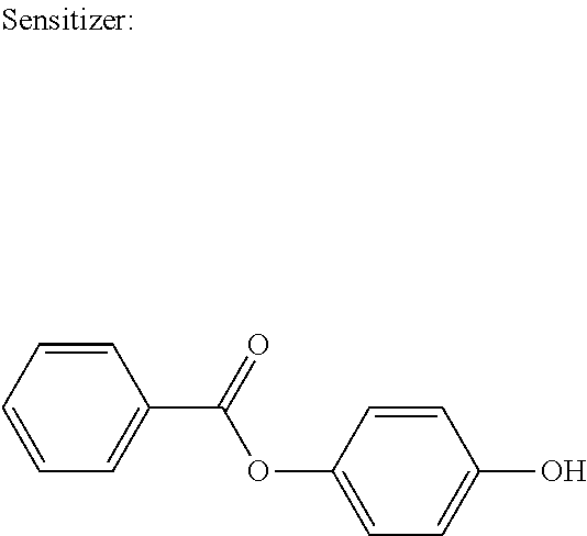
Surfactant: FC-4430 Manufactured by 3M
| TABLE 3 | |||||
| Components | Polymer | Quencher | Sensitizer | Surfactant | Organic solvent |
| Composition | (100) | (4.0) | (2.1) | (0.25) | PGMEA (400) |
| (parts by | CyHO (2000) | ||||
| mass) | PGME (100) | ||||
| Organic solvent: PGMEA (propylene glycol monomethyl ether acetate) CyHO (cyclohexanone) PGME (propylene glycol monomethyl ether) | |||||
| TABLE 4 | |||||
| Polysiloxane | |||||
| resist | |||||
| underlayer | Sensitivity | CDU | |||
| Examples | film | (mJ/cm2) | (nm) | ||
| Example 1 | Film 1 | 22 | 3.1 | ||
| Example 2 | Film 2 | 24 | 3.0 | ||
| Example 3 | Film 3 | 22 | 3.1 | ||
| Example 4 | Film 4 | 23 | 3.0 | ||
| Example 5 | Film 5 | 23 | 3.2 | ||
| Example 6 | Film 6 | 23 | 3.0 | ||
| Example 7 | Film 7 | 23 | 3.0 | ||
| Example 8 | Film 8 | 23 | 3.0 | ||
| Example 9 | Film 9 | 23 | 2.9 | ||
| Example 10 | Film 10 | 23 | 3.1 | ||
| Example 11 | Film 11 | 24 | 3.2 | ||
| Example 12 | Film 12 | 22 | 3.2 | ||
| Example 13 | Film 13 | 23 | 3.0 | ||
| Example 14 | Film 14 | 23 | 3.1 | ||
| Example 15 | Film 15 | 22 | 3.0 | ||
| Example 16 | Film 16 | 24 | 3.0 | ||
| Example 17 | Film 17 | 24 | 2.8 | ||
| Example 18 | Film 18 | 22 | 2.9 | ||
| Example 19 | Film 19 | 24 | 2.8 | ||
| Example 20 | Film 20 | 24 | 3.0 | ||
| Example 21 | Film 21 | 22 | 3.2 | ||
| Example 22 | Film 22 | 22 | 3.0 | ||
| Example 23 | Film 23 | 23 | 2.9 | ||
| Example 24 | Film 24 | 22 | 2.9 | ||
| Example 25 | Film 25 | 23 | 2.8 | ||
| Example 26 | Film 26 | 22 | 2.9 | ||
| Example 27 | Film 27 | 22 | 3.0 | ||
| Example 28 | Film 28 | 22 | 2.8 | ||
| Example 29 | Film 29 | 22 | 2.9 | ||
| Example 30 | Film 30 | 24 | 2.9 | ||
| Example 31 | Film 31 | 23 | 3.0 | ||
| Example 32 | Film 32 | 24 | 3.0 | ||
| Example 33 | Film 33 | 22 | 3.1 | ||
| Comparative | Film 34 | 28 | 3.3 | ||
| Example 1 | |||||
| Comparative | Film 35 | 29 | 3.1 | ||
| Example 2 | |||||
| Comparative | Film 36 | 27 | 3.1 | ||
| Example 3 | |||||
| Comparative | Film 37 | 27 | 3.2 | ||
| Example 4 | |||||
| Comparative | Film 38 | 28 | 3.0 | ||
| Example 5 | |||||
| Comparative | Film 39 | 28 | 3.2 | ||
| Example 6 | |||||
Claims (12)


Priority Applications (1)
| Application Number | Priority Date | Filing Date | Title |
|---|---|---|---|
| US18/340,442 US12332565B2 (en) | 2018-11-21 | 2023-06-23 | Thermosetting iodine- and silicon-containing material, composition containing the material for forming resist underlayer film for EUV lithography, and patterning process |
Applications Claiming Priority (4)
| Application Number | Priority Date | Filing Date | Title |
|---|---|---|---|
| JP2018218483 | 2018-11-21 | ||
| JP2018-218483 | 2018-11-21 | ||
| US16/660,992 US11914295B2 (en) | 2018-11-21 | 2019-10-23 | Thermosetting iodine- and silicon-containing material, composition containing the material for forming resist underlayer film for EUV lithography, and patterning process |
| US18/340,442 US12332565B2 (en) | 2018-11-21 | 2023-06-23 | Thermosetting iodine- and silicon-containing material, composition containing the material for forming resist underlayer film for EUV lithography, and patterning process |
Related Parent Applications (1)
| Application Number | Title | Priority Date | Filing Date |
|---|---|---|---|
| US16/660,992 Division US11914295B2 (en) | 2018-11-21 | 2019-10-23 | Thermosetting iodine- and silicon-containing material, composition containing the material for forming resist underlayer film for EUV lithography, and patterning process |
Publications (2)
| Publication Number | Publication Date |
|---|---|
| US20230333472A1 US20230333472A1 (en) | 2023-10-19 |
| US12332565B2 true US12332565B2 (en) | 2025-06-17 |
Family
ID=68653413
Family Applications (2)
| Application Number | Title | Priority Date | Filing Date |
|---|---|---|---|
| US16/660,992 Active 2040-07-04 US11914295B2 (en) | 2018-11-21 | 2019-10-23 | Thermosetting iodine- and silicon-containing material, composition containing the material for forming resist underlayer film for EUV lithography, and patterning process |
| US18/340,442 Active US12332565B2 (en) | 2018-11-21 | 2023-06-23 | Thermosetting iodine- and silicon-containing material, composition containing the material for forming resist underlayer film for EUV lithography, and patterning process |
Family Applications Before (1)
| Application Number | Title | Priority Date | Filing Date |
|---|---|---|---|
| US16/660,992 Active 2040-07-04 US11914295B2 (en) | 2018-11-21 | 2019-10-23 | Thermosetting iodine- and silicon-containing material, composition containing the material for forming resist underlayer film for EUV lithography, and patterning process |
Country Status (6)
| Country | Link |
|---|---|
| US (2) | US11914295B2 (en) |
| EP (1) | EP3657254B1 (en) |
| JP (2) | JP7357505B2 (en) |
| KR (1) | KR102316373B1 (en) |
| CN (1) | CN111208710B (en) |
| TW (1) | TWI756588B (en) |
Families Citing this family (17)
| Publication number | Priority date | Publication date | Assignee | Title |
|---|---|---|---|---|
| JP7406300B2 (en) * | 2018-11-12 | 2023-12-27 | 信越化学工業株式会社 | Method for producing iodine-containing silicon compound |
| JP7357505B2 (en) * | 2018-11-21 | 2023-10-06 | 信越化学工業株式会社 | Iodine-containing thermosetting silicon-containing material, composition for forming a resist underlayer film for EUV lithography containing the same, and pattern forming method |
| JP7282667B2 (en) * | 2019-01-22 | 2023-05-29 | 信越化学工業株式会社 | Composition for forming silicon-containing resist underlayer film and pattern forming method |
| JP7368324B2 (en) | 2019-07-23 | 2023-10-24 | 信越化学工業株式会社 | Composition for forming silicon-containing resist underlayer film and pattern forming method |
| TW202113488A (en) * | 2019-08-21 | 2021-04-01 | 美商布魯爾科技公司 | Underlayers for euv lithography |
| EP4200307A1 (en) * | 2020-08-19 | 2023-06-28 | Henkel AG & Co. KGaA | Heteroatom-containing silane compound |
| WO2022113781A1 (en) * | 2020-11-26 | 2022-06-02 | Jsr株式会社 | Silicon-containing composition and method for producing semiconductor substrate |
| US20240295819A1 (en) * | 2021-06-11 | 2024-09-05 | Nissan Chemical Corporation | Composition for forming silicon-containing resist underlayer film |
| JP7698607B2 (en) * | 2022-06-10 | 2025-06-25 | 信越化学工業株式会社 | Resist underlayer film material, pattern forming method, and resist underlayer film forming method |
| WO2023243579A1 (en) * | 2022-06-14 | 2023-12-21 | セントラル硝子株式会社 | Electronic device manufacturing method and laminate |
| US20240096623A1 (en) * | 2022-08-31 | 2024-03-21 | Taiwan Semiconductor Manufacturing Company, Ltd. | Method of manufacturing a semiconductor device |
| JPWO2024070786A1 (en) * | 2022-09-30 | 2024-04-04 | ||
| EP4679175A1 (en) | 2023-03-03 | 2026-01-14 | Nissan Chemical Corporation | Composition for forming silicon-containing resist underlayer film |
| JP2025113920A (en) | 2024-01-23 | 2025-08-04 | 信越化学工業株式会社 | Composition for forming metal-containing film, pattern forming method |
| JP2025113925A (en) | 2024-01-23 | 2025-08-04 | 信越化学工業株式会社 | Adhesion film forming composition and pattern forming method |
| JP2025139452A (en) * | 2024-03-12 | 2025-09-26 | 信越化学工業株式会社 | Polyvalent ammonium salt compound, composition for forming silicon-containing resist underlayer film, and pattern forming method |
| JP2025180058A (en) | 2024-05-29 | 2025-12-11 | 信越化学工業株式会社 | Method for forming metal-containing film pattern |
Citations (22)
| Publication number | Priority date | Publication date | Assignee | Title |
|---|---|---|---|---|
| US3669796A (en) | 1968-10-03 | 1972-06-13 | Scm Corp | Adhering resins to substrates,especially metal,by radiation |
| JPS6017443A (en) | 1983-07-11 | 1985-01-29 | Nippon Telegr & Teleph Corp <Ntt> | Pattern forming material and formation of pattern |
| JPS6080844A (en) | 1983-10-11 | 1985-05-08 | Nippon Telegr & Teleph Corp <Ntt> | Pattern forming material and formation of pattern |
| US4564579A (en) | 1983-04-18 | 1986-01-14 | Nippon Telegraph & Telephone Public Corporation | Pattern forming material of a siloxane polymer |
| JPH04107461A (en) | 1990-08-28 | 1992-04-08 | Oki Electric Ind Co Ltd | Photosensitive resin composition |
| US20040236057A1 (en) | 2001-07-28 | 2004-11-25 | Pierre Chevalier | High refractive index polysiloxanes and their preparation |
| TW200846400A (en) | 2007-02-01 | 2008-12-01 | Sumitomo Chemical Co | Manufacturing method of structure comprising aromatic polymer bonded to substrate, structure comprising aromatic polymer chain bonded to electroconductive substrate, and electronic device containing the structure |
| US20090136869A1 (en) | 2007-11-22 | 2009-05-28 | Tsutomu Ogihara | Metal oxide-containing film-forming composition, metal oxide-containing film, metal oxide-containing film-bearing substrate, and patterning method |
| US20120052685A1 (en) | 2010-09-01 | 2012-03-01 | Shin-Etsu Chemical Co., Ltd. | Silicon-containing film-forming composition, silicon-containing film-formed substrate, and patterning process |
| WO2013051558A1 (en) | 2011-10-06 | 2013-04-11 | 日産化学工業株式会社 | Composition for forming silicon-containing euv resist underlayer film |
| US20130210236A1 (en) | 2012-02-14 | 2013-08-15 | Shin-Etsu Chemical Co., Ltd. | Silicon-containing surface modifier, resist underlayer film composition containing this, and patterning process |
| US20130280912A1 (en) | 2012-04-23 | 2013-10-24 | Shin-Etsu Chemical Co., Ltd. | Silicon compound, silicon-containing compound, composition for forming resist underlayer film containing the same and patterning process |
| US20130323645A1 (en) | 2012-05-30 | 2013-12-05 | Tokyo Ohka Kogyo Co., Ltd. | Resist composition, method of forming resist pattern, and compound |
| US20140235796A1 (en) | 2013-02-15 | 2014-08-21 | Shin-Etsu Chemical Co., Ltd. | Composition for forming resist underlayer film and patterning process |
| WO2016093172A1 (en) | 2014-12-08 | 2016-06-16 | 日産化学工業株式会社 | Resist underlayer film forming composition for lithography containing hydrolyzable silane having halogen-containing carboxylic acid amide group |
| US20170154766A1 (en) | 2015-11-27 | 2017-06-01 | Shin-Etsu Chemical Co., Ltd. | Silicon-containing condensate, composition for forming a silicon-containing resist under layer film, and patterning process |
| US20180267402A1 (en) | 2017-03-17 | 2018-09-20 | Shin-Etsu Chemical Co., Ltd. | Resist composition and patterning process |
| US20180292753A1 (en) | 2017-03-23 | 2018-10-11 | Jsr Corporation | Composition for forming silicon-containing film for euv lithography, silicon-containing film for euv lithography, and pattern-forming method |
| US20180366319A1 (en) * | 2017-06-14 | 2018-12-20 | Rohm And Haas Electronic Materials Llc | Silicon-based hardmask |
| US20200159120A1 (en) | 2018-11-21 | 2020-05-21 | Shin-Etsu Chemical Co., Ltd. | Thermosetting iodine- and silicon-containing material, composition containing the material for forming resist underlayer film for euv lithography, and patterning process |
| US20200233303A1 (en) | 2019-01-22 | 2020-07-23 | Shin-Etsu Chemical Co., Ltd. | Composition for forming silicon-containing resist underlayer film and patterning process |
| US20200319550A1 (en) | 2019-04-05 | 2020-10-08 | Shin-Etsu Chemical Co., Ltd. | Sulfonium compound, chemically amplified resist composition, and patterning process |
Family Cites Families (23)
| Publication number | Priority date | Publication date | Assignee | Title |
|---|---|---|---|---|
| JP2004153125A (en) | 2002-10-31 | 2004-05-27 | Fujitsu Ltd | Method of forming processing mask and method of manufacturing semiconductor device |
| JP4355943B2 (en) | 2003-10-03 | 2009-11-04 | 信越化学工業株式会社 | Photoresist underlayer film forming material and pattern forming method |
| US7303855B2 (en) | 2003-10-03 | 2007-12-04 | Shin-Etsu Chemical Co., Ltd. | Photoresist undercoat-forming material and patterning process |
| JP4562784B2 (en) | 2007-04-13 | 2010-10-13 | 富士フイルム株式会社 | PATTERN FORMING METHOD, RESIST COMPOSITION, DEVELOPER AND RINSE SOLUTION USED FOR THE PATTERN FORMING METHOD |
| JP4982288B2 (en) | 2007-04-13 | 2012-07-25 | 富士フイルム株式会社 | Pattern formation method |
| JP5002379B2 (en) | 2007-04-13 | 2012-08-15 | 富士フイルム株式会社 | Pattern formation method |
| US8034547B2 (en) | 2007-04-13 | 2011-10-11 | Fujifilm Corporation | Pattern forming method, resist composition to be used in the pattern forming method, negative developing solution to be used in the pattern forming method and rinsing solution for negative development to be used in the pattern forming method |
| JP5387181B2 (en) | 2009-07-08 | 2014-01-15 | 信越化学工業株式会社 | Sulfonium salt, resist material and pattern forming method |
| CN102051121A (en) * | 2009-12-02 | 2011-05-11 | 合肥凯蒙新材料有限公司 | Antireflection coating for 193-nano-wavelength photolithography and preparation method and application thereof |
| JP5518772B2 (en) | 2011-03-15 | 2014-06-11 | 信越化学工業株式会社 | Pattern formation method |
| JP5785121B2 (en) | 2011-04-28 | 2015-09-24 | 信越化学工業株式会社 | Pattern formation method |
| JP5650086B2 (en) | 2011-06-28 | 2015-01-07 | 信越化学工業株式会社 | Resist underlayer film forming composition and pattern forming method |
| JP5453361B2 (en) | 2011-08-17 | 2014-03-26 | 信越化学工業株式会社 | Silicon-containing resist underlayer film forming composition and pattern forming method |
| JP5746005B2 (en) | 2011-11-29 | 2015-07-08 | 信越化学工業株式会社 | Silicon-containing resist underlayer film forming composition and pattern forming method |
| JP5739360B2 (en) | 2012-02-14 | 2015-06-24 | 信越化学工業株式会社 | Silicon-containing resist underlayer film forming composition and pattern forming method |
| US9164384B2 (en) | 2013-04-26 | 2015-10-20 | Shin-Etsu Chemical Co., Ltd. | Patterning process and resist composition |
| CN115016230A (en) | 2014-07-15 | 2022-09-06 | 日产化学工业株式会社 | Composition for forming silicon-containing resist underlayer film |
| TW201612249A (en) | 2014-09-29 | 2016-04-01 | Fujifilm Corp | Photosensitive resin composition, manufacturing method for cured film, cured film, liquid crystal display device, organic electroluminescence display device and touch panel |
| JP6673105B2 (en) * | 2016-08-31 | 2020-03-25 | 信越化学工業株式会社 | Sulfonium compound, resist composition and pattern forming method |
| WO2018159356A1 (en) | 2017-03-02 | 2018-09-07 | Jsr株式会社 | Composition for silicon-containing-film formation, silicon-containing film, pattern formation method, and polysiloxane |
| JP6904302B2 (en) | 2017-06-14 | 2021-07-14 | 信越化学工業株式会社 | Resist material and pattern formation method |
| JP6950357B2 (en) | 2017-08-24 | 2021-10-13 | 信越化学工業株式会社 | Sulfonium compound, resist composition and pattern forming method |
| JP7360927B2 (en) | 2019-01-09 | 2023-10-13 | 信越化学工業株式会社 | Thermosetting silicon-containing compound, silicon-containing film forming composition, and pattern forming method |
-
2019
- 2019-10-04 JP JP2019183751A patent/JP7357505B2/en active Active
- 2019-10-23 US US16/660,992 patent/US11914295B2/en active Active
- 2019-11-20 TW TW108142057A patent/TWI756588B/en active
- 2019-11-20 CN CN201911139299.8A patent/CN111208710B/en active Active
- 2019-11-20 KR KR1020190149730A patent/KR102316373B1/en active Active
- 2019-11-21 EP EP19210759.7A patent/EP3657254B1/en active Active
-
2023
- 2023-05-26 JP JP2023086699A patent/JP7478884B2/en active Active
- 2023-06-23 US US18/340,442 patent/US12332565B2/en active Active
Patent Citations (37)
| Publication number | Priority date | Publication date | Assignee | Title |
|---|---|---|---|---|
| US3669796A (en) | 1968-10-03 | 1972-06-13 | Scm Corp | Adhering resins to substrates,especially metal,by radiation |
| US4564579A (en) | 1983-04-18 | 1986-01-14 | Nippon Telegraph & Telephone Public Corporation | Pattern forming material of a siloxane polymer |
| JPS6017443A (en) | 1983-07-11 | 1985-01-29 | Nippon Telegr & Teleph Corp <Ntt> | Pattern forming material and formation of pattern |
| JPS6080844A (en) | 1983-10-11 | 1985-05-08 | Nippon Telegr & Teleph Corp <Ntt> | Pattern forming material and formation of pattern |
| JPH04107461A (en) | 1990-08-28 | 1992-04-08 | Oki Electric Ind Co Ltd | Photosensitive resin composition |
| US20040236057A1 (en) | 2001-07-28 | 2004-11-25 | Pierre Chevalier | High refractive index polysiloxanes and their preparation |
| JP2004536210A (en) | 2001-07-28 | 2004-12-02 | ダウ・コ−ニング・コ−ポレ−ション | High refractive index polysiloxanes and their preparation |
| US20100069603A1 (en) | 2007-02-01 | 2010-03-18 | Sumitomo Chemical Company, Limited | Method for producing structure wherein aromatic polymer is bonded to base, structure having aromatic polymer chain bonded to conductive base, and electronic device comprising the structure |
| TW200846400A (en) | 2007-02-01 | 2008-12-01 | Sumitomo Chemical Co | Manufacturing method of structure comprising aromatic polymer bonded to substrate, structure comprising aromatic polymer chain bonded to electroconductive substrate, and electronic device containing the structure |
| US20090136869A1 (en) | 2007-11-22 | 2009-05-28 | Tsutomu Ogihara | Metal oxide-containing film-forming composition, metal oxide-containing film, metal oxide-containing film-bearing substrate, and patterning method |
| JP2009126940A (en) | 2007-11-22 | 2009-06-11 | Shin Etsu Chem Co Ltd | Metal oxide-containing film forming composition, metal oxide-containing film, metal oxide-containing film forming substrate, and pattern forming method using the same |
| US20120052685A1 (en) | 2010-09-01 | 2012-03-01 | Shin-Etsu Chemical Co., Ltd. | Silicon-containing film-forming composition, silicon-containing film-formed substrate, and patterning process |
| EP2426558A1 (en) | 2010-09-01 | 2012-03-07 | Shin-Etsu Chemical Co., Ltd. | Silicon-containing film-forming composition, silicon-containing film-formed substrate, and patterning process |
| JP2012053253A (en) | 2010-09-01 | 2012-03-15 | Shin Etsu Chem Co Ltd | Composition for forming silicon-containing film, silicon-containing film-formed substrate and pattern forming method using the same |
| KR20140089350A (en) | 2011-10-06 | 2014-07-14 | 닛산 가가쿠 고교 가부시키 가이샤 | Composition for forming silicon-containing euv resist underlayer film |
| WO2013051558A1 (en) | 2011-10-06 | 2013-04-11 | 日産化学工業株式会社 | Composition for forming silicon-containing euv resist underlayer film |
| US20140232018A1 (en) | 2011-10-06 | 2014-08-21 | Nissan Chemical Industries, Ltd. | Silicon-containing euv resist underlayer film forming composition |
| US20130210236A1 (en) | 2012-02-14 | 2013-08-15 | Shin-Etsu Chemical Co., Ltd. | Silicon-containing surface modifier, resist underlayer film composition containing this, and patterning process |
| EP2628744A1 (en) | 2012-02-14 | 2013-08-21 | Shin-Etsu Chemical Co., Ltd. | Silicon-containing surface modifier, resist underlayer film composition containing this, and patterning process |
| JP2013167669A (en) | 2012-02-14 | 2013-08-29 | Shin Etsu Chem Co Ltd | Silicon-containing surface modifier, composition for forming resist underlayer film containing the same, and patterning process |
| US20130280912A1 (en) | 2012-04-23 | 2013-10-24 | Shin-Etsu Chemical Co., Ltd. | Silicon compound, silicon-containing compound, composition for forming resist underlayer film containing the same and patterning process |
| JP2013224279A (en) | 2012-04-23 | 2013-10-31 | Shin-Etsu Chemical Co Ltd | Silicon compound, silicon-containing compound, composition for forming resist underlayer film containing the same and patterning process |
| JP2014006489A (en) | 2012-05-30 | 2014-01-16 | Tokyo Ohka Kogyo Co Ltd | Resist composition, method for forming resist pattern, and compound |
| US20130323645A1 (en) | 2012-05-30 | 2013-12-05 | Tokyo Ohka Kogyo Co., Ltd. | Resist composition, method of forming resist pattern, and compound |
| US20140235796A1 (en) | 2013-02-15 | 2014-08-21 | Shin-Etsu Chemical Co., Ltd. | Composition for forming resist underlayer film and patterning process |
| JP2014157242A (en) | 2013-02-15 | 2014-08-28 | Shin Etsu Chem Co Ltd | Composition for forming resist underlayer film and patterning process |
| US20170322491A1 (en) | 2014-12-08 | 2017-11-09 | Nissan Chemical Industries, Ltd. | Resist underlayer film forming composition for lithography containing hydrolyzable silane having halogen-containing carboxylic acid amide group |
| WO2016093172A1 (en) | 2014-12-08 | 2016-06-16 | 日産化学工業株式会社 | Resist underlayer film forming composition for lithography containing hydrolyzable silane having halogen-containing carboxylic acid amide group |
| US20170154766A1 (en) | 2015-11-27 | 2017-06-01 | Shin-Etsu Chemical Co., Ltd. | Silicon-containing condensate, composition for forming a silicon-containing resist under layer film, and patterning process |
| JP2017095643A (en) | 2015-11-27 | 2017-06-01 | 信越化学工業株式会社 | Silicon containing condensate, silicon containing resist underlay film forming composition, and pattern forming method |
| US20180267402A1 (en) | 2017-03-17 | 2018-09-20 | Shin-Etsu Chemical Co., Ltd. | Resist composition and patterning process |
| KR20180106938A (en) | 2017-03-17 | 2018-10-01 | 신에쓰 가가꾸 고교 가부시끼가이샤 | Resist composition and patterning process |
| US20180292753A1 (en) | 2017-03-23 | 2018-10-11 | Jsr Corporation | Composition for forming silicon-containing film for euv lithography, silicon-containing film for euv lithography, and pattern-forming method |
| US20180366319A1 (en) * | 2017-06-14 | 2018-12-20 | Rohm And Haas Electronic Materials Llc | Silicon-based hardmask |
| US20200159120A1 (en) | 2018-11-21 | 2020-05-21 | Shin-Etsu Chemical Co., Ltd. | Thermosetting iodine- and silicon-containing material, composition containing the material for forming resist underlayer film for euv lithography, and patterning process |
| US20200233303A1 (en) | 2019-01-22 | 2020-07-23 | Shin-Etsu Chemical Co., Ltd. | Composition for forming silicon-containing resist underlayer film and patterning process |
| US20200319550A1 (en) | 2019-04-05 | 2020-10-08 | Shin-Etsu Chemical Co., Ltd. | Sulfonium compound, chemically amplified resist composition, and patterning process |
Non-Patent Citations (9)
| Title |
|---|
| Apr. 29, 2020 Extended Search Report issued in European Patent Application No. 19210759.7. |
| Apr. 8, 2024 Office Action issued in U.S. Appl. No. 18/184,709. |
| Feb. 22, 2021 Office Action issued in Korean Patent Application No. 10-2019-0149730. |
| Feb. 28, 2023 Office Action issued in Japanese Application 2019-183751. |
| Feb. 3, 2021 Office Action issued in Taiwanese Application No. 108142057. |
| Hutchinson. John M., "The Shot Noise Impact on Resist Roughness in EUV Lithography", SPIE, vol. 3331, pp. 531-536, (1998). |
| Nov. 2, 2021 Office Action issued in Taiwanese Application No. 108142057. |
| Sep. 27, 2022 Office Action issued in Japanese Application No. 2019-183751. |
| Yoshifumi, Maegawa et al., "A New Synthetic Approach for Functional Triisopropoxyorganosilanes Using Molecular Building Blocks", Tetrhedron, Elsevier Science Publishers, Amsterdam, NL, vol. 69, No. 26, pp. 5312-5318, XP028551479. |
Also Published As
| Publication number | Publication date |
|---|---|
| JP7357505B2 (en) | 2023-10-06 |
| TWI756588B (en) | 2022-03-01 |
| US20230333472A1 (en) | 2023-10-19 |
| KR20200060278A (en) | 2020-05-29 |
| EP3657254A1 (en) | 2020-05-27 |
| JP2020084175A (en) | 2020-06-04 |
| US11914295B2 (en) | 2024-02-27 |
| JP2023116531A (en) | 2023-08-22 |
| CN111208710A (en) | 2020-05-29 |
| KR102316373B1 (en) | 2021-10-21 |
| US20200159120A1 (en) | 2020-05-21 |
| JP7478884B2 (en) | 2024-05-07 |
| EP3657254B1 (en) | 2021-06-16 |
| TW202026339A (en) | 2020-07-16 |
| CN111208710B (en) | 2023-08-22 |
Similar Documents
| Publication | Publication Date | Title |
|---|---|---|
| US12332565B2 (en) | Thermosetting iodine- and silicon-containing material, composition containing the material for forming resist underlayer film for EUV lithography, and patterning process | |
| US11385544B2 (en) | Composition for forming silicon-containing resist underlayer film and patterning process | |
| US11480879B2 (en) | Composition for forming silicon-containing resist underlayer film and patterning process | |
| US12174541B2 (en) | Composition for forming silicon-containing resist underlayer film and patterning process | |
| US11485824B2 (en) | Thermosetting silicon-containing compound, composition for forming a silicon-containing film, and patterning process | |
| US12001138B2 (en) | Composition for forming silicon-containing resist underlayer film and patterning process | |
| US12332567B2 (en) | Composition for forming silicon-containing resist underlayer film, patterning process, and silicon compound | |
| US20240319598A1 (en) | Composition For Forming Silicon-Containing Resist Underlayer Film And Patterning Process | |
| US20250289931A1 (en) | Polyvalent ammonium salt compound, composition for forming silicon-containing resist underlayer film, and patterning process | |
| US20250237953A1 (en) | Silicon-containing sulfonium salt compound, composition for forming a silicon-containing resist underlayer film, and patterning process |
Legal Events
| Date | Code | Title | Description |
|---|---|---|---|
| FEPP | Fee payment procedure |
Free format text: ENTITY STATUS SET TO UNDISCOUNTED (ORIGINAL EVENT CODE: BIG.); ENTITY STATUS OF PATENT OWNER: LARGE ENTITY |
|
| STPP | Information on status: patent application and granting procedure in general |
Free format text: DOCKETED NEW CASE - READY FOR EXAMINATION |
|
| STPP | Information on status: patent application and granting procedure in general |
Free format text: NON FINAL ACTION MAILED |
|
| STPP | Information on status: patent application and granting procedure in general |
Free format text: RESPONSE TO NON-FINAL OFFICE ACTION ENTERED AND FORWARDED TO EXAMINER |
|
| STPP | Information on status: patent application and granting procedure in general |
Free format text: FINAL REJECTION MAILED |
|
| STPP | Information on status: patent application and granting procedure in general |
Free format text: RESPONSE AFTER FINAL ACTION FORWARDED TO EXAMINER |
|
| STPP | Information on status: patent application and granting procedure in general |
Free format text: ADVISORY ACTION MAILED |
|
| STPP | Information on status: patent application and granting procedure in general |
Free format text: DOCKETED NEW CASE - READY FOR EXAMINATION |
|
| STPP | Information on status: patent application and granting procedure in general |
Free format text: NOTICE OF ALLOWANCE MAILED -- APPLICATION RECEIVED IN OFFICE OF PUBLICATIONS |
|
| STCF | Information on status: patent grant |
Free format text: PATENTED CASE |