US12310053B2 - Super-junction VDMOS device with low on-resistance - Google Patents
Super-junction VDMOS device with low on-resistance Download PDFInfo
- Publication number
- US12310053B2 US12310053B2 US18/054,557 US202218054557A US12310053B2 US 12310053 B2 US12310053 B2 US 12310053B2 US 202218054557 A US202218054557 A US 202218054557A US 12310053 B2 US12310053 B2 US 12310053B2
- Authority
- US
- United States
- Prior art keywords
- super
- pillar
- semiconductor
- junction
- region
- Prior art date
- Legal status (The legal status is an assumption and is not a legal conclusion. Google has not performed a legal analysis and makes no representation as to the accuracy of the status listed.)
- Active, expires
Links
Images


Classifications
-
- H—ELECTRICITY
- H10—SEMICONDUCTOR DEVICES; ELECTRIC SOLID-STATE DEVICES NOT OTHERWISE PROVIDED FOR
- H10D—INORGANIC ELECTRIC SEMICONDUCTOR DEVICES
- H10D30/00—Field-effect transistors [FET]
- H10D30/60—Insulated-gate field-effect transistors [IGFET]
- H10D30/64—Double-diffused metal-oxide semiconductor [DMOS] FETs
- H10D30/66—Vertical DMOS [VDMOS] FETs
- H10D30/668—Vertical DMOS [VDMOS] FETs having trench gate electrodes, e.g. UMOS transistors
-
- H—ELECTRICITY
- H10—SEMICONDUCTOR DEVICES; ELECTRIC SOLID-STATE DEVICES NOT OTHERWISE PROVIDED FOR
- H10D—INORGANIC ELECTRIC SEMICONDUCTOR DEVICES
- H10D62/00—Semiconductor bodies, or regions thereof, of devices having potential barriers
- H10D62/10—Shapes, relative sizes or dispositions of the regions of the semiconductor bodies; Shapes of the semiconductor bodies
- H10D62/102—Constructional design considerations for preventing surface leakage or controlling electric field concentration
- H10D62/103—Constructional design considerations for preventing surface leakage or controlling electric field concentration for increasing or controlling the breakdown voltage of reverse-biased devices
- H10D62/105—Constructional design considerations for preventing surface leakage or controlling electric field concentration for increasing or controlling the breakdown voltage of reverse-biased devices by having particular doping profiles, shapes or arrangements of PN junctions; by having supplementary regions, e.g. junction termination extension [JTE]
- H10D62/109—Reduced surface field [RESURF] PN junction structures
- H10D62/111—Multiple RESURF structures, e.g. double RESURF or 3D-RESURF structures
-
- H—ELECTRICITY
- H10—SEMICONDUCTOR DEVICES; ELECTRIC SOLID-STATE DEVICES NOT OTHERWISE PROVIDED FOR
- H10D—INORGANIC ELECTRIC SEMICONDUCTOR DEVICES
- H10D62/00—Semiconductor bodies, or regions thereof, of devices having potential barriers
- H10D62/10—Shapes, relative sizes or dispositions of the regions of the semiconductor bodies; Shapes of the semiconductor bodies
- H10D62/124—Shapes, relative sizes or dispositions of the regions of semiconductor bodies or of junctions between the regions
-
- H—ELECTRICITY
- H10—SEMICONDUCTOR DEVICES; ELECTRIC SOLID-STATE DEVICES NOT OTHERWISE PROVIDED FOR
- H10D—INORGANIC ELECTRIC SEMICONDUCTOR DEVICES
- H10D62/00—Semiconductor bodies, or regions thereof, of devices having potential barriers
- H10D62/80—Semiconductor bodies, or regions thereof, of devices having potential barriers characterised by the materials
- H10D62/82—Heterojunctions
-
- H—ELECTRICITY
- H10—SEMICONDUCTOR DEVICES; ELECTRIC SOLID-STATE DEVICES NOT OTHERWISE PROVIDED FOR
- H10D—INORGANIC ELECTRIC SEMICONDUCTOR DEVICES
- H10D62/00—Semiconductor bodies, or regions thereof, of devices having potential barriers
- H10D62/80—Semiconductor bodies, or regions thereof, of devices having potential barriers characterised by the materials
- H10D62/83—Semiconductor bodies, or regions thereof, of devices having potential barriers characterised by the materials being Group IV materials, e.g. B-doped Si or undoped Ge
- H10D62/832—Semiconductor bodies, or regions thereof, of devices having potential barriers characterised by the materials being Group IV materials, e.g. B-doped Si or undoped Ge being Group IV materials comprising two or more elements, e.g. SiGe
- H10D62/8325—Silicon carbide
-
- H—ELECTRICITY
- H10—SEMICONDUCTOR DEVICES; ELECTRIC SOLID-STATE DEVICES NOT OTHERWISE PROVIDED FOR
- H10D—INORGANIC ELECTRIC SEMICONDUCTOR DEVICES
- H10D62/00—Semiconductor bodies, or regions thereof, of devices having potential barriers
- H10D62/80—Semiconductor bodies, or regions thereof, of devices having potential barriers characterised by the materials
- H10D62/85—Semiconductor bodies, or regions thereof, of devices having potential barriers characterised by the materials being Group III-V materials, e.g. GaAs
- H10D62/8503—Nitride Group III-V materials, e.g. AlN or GaN
Definitions
- the present disclosure relates to power semiconductor devices, in particular, to a super-junction VDMOS device with a low on-resistance.
- VDMOSFET vertical double-diffused metal oxide semiconductor field effect transistor
- bipolar transistors are advantageous for their high switching speed, low power loss, high input impedance, low driving power, good frequency characteristics, and high transconductance linearity. Therefore, VDMOS devices have been widely adopted in modern power devices.
- conventional VDMOS devices come with inherent disadvantages.
- the on-resistance increases with the breakdown voltage in conventional VDMOS devices, which further leads to a rapid increase in power consumption.
- charge-balancing devices such as super-junction VDMOS devices
- super-junction VDMOS devices has the capability of reducing the constraint between the on-resistance and the breakdown voltage, and simultaneously achieving a low on-state power consumption and a high blocking voltage.
- super-junction VDMOS devices are now applied in various energy-efficient scenarios and have a promising future.
- a power super-junction VDMOS device have alternately arranged P-pillars and N-pillars, unlike traditional power devices, which are based on N drifting regions.
- a power super-junction VDMOS device When a power super-junction VDMOS device is in a cut-off state and reverse-biased, the combined effect of a transverse electric field (e.g., in x direction) and a longitudinal electric field (e.g., in y direction) will cause the P-pillars and the N-pillars to be completely depleted.
- the longitudinal electric field in the depletion region tends to be uniform, and therefore, the breakdown voltage is theoretically dependent only on the thickness of the voltage withstanding layer, but irrelevant to the dopant concentration of the voltage withstanding layer.
- the dopant concentration of the voltage withstanding layer can be increased by nearly an order of magnitude, which effectively reduces the on-resistance of the power super-junction VDMOS device and the power consumption.
- the super-junction VDMOS device in conventional arts is limited by its materials, the migration rate of carriers in the materials, and the tradeoffs between the on-resistance and breakdown voltage. Therefore, it is technically difficult to further reduce the on-resistance of the VDMOS device.
- the present disclosure provides a super-junction vertical double-diffused metal oxide semiconductor field effect transistor (VDMOS) device with a low on-resistance, comprising: a drain region, which is of a first dopant type; a super-junction structure, disposed on the drain region; a body region, which is of a second dopant type and disposed on the super-junction structure; a source region, which is of the first dopant type; and a gate structure; wherein the super-junction structure comprises a first semiconductor pillar, which is of the first dopant type, and a second semiconductor pillar, which is of the second dopant type, wherein the first semiconductor pillar and the second semiconductor pillar are alternately arranged and are adjacent to each other, wherein the second semiconductor pillar is disposed below the body region, and the first semiconductor pillar is disposed below the gate structure, wherein a high-electron-mobility transistor (HEMT) structure formed by heterojunctions is disposed at an interface between the first semiconductor pillar
- the drain region, the super-junction structure, the body region, and the source region comprise SiC; the first semiconductor material pillar comprise GaN; the second semiconductor material pillar comprise AlGaN.
- the drain region, the super-junction structure, the body region and the first type semiconductor source region comprise 4H—SiC.
- the drain region, the super-junction structure, the body region, and the source region comprise Si; the first semiconductor material pillar comprises GaAs; the second semiconductor material pillar comprises AlGaAs.
- the first dopant type is N type, and the second dopant type is P type; or the first dopant type is P type, and the second dopant type is N type.
- the gate structure is of a planar gate structure or of a trench gate structure.
- the drain region is in ohmic contact with a metal drain electrode.
- the body region comprises an ohmic contact layer, which is of the second dopant type.
- the ohmic contact layer and the source region are in ohmic contact with the metal source electrode.
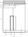
- FIG. 1 shows a schematic cross-section of a super-junction VDMOS device with a low on-resistance according to one or more embodiments of the present disclosure, wherein its gate is of a planar gate structure.
- FIG. 2 shows a schematic cross-section of a super-junction VDMOS device with a low on-resistance according to one or more embodiments of the present disclosure, whose gate has a trench gate structure.
- FIG. 3 shows energy bands of materials of a super-junction VDMOS device with a low on-resistance according to one or more embodiments of the present disclosure, when the materials are not in contact with each other.
- FIGS. 1 through 4 it should be noted that the drawings provided in the embodiments illustrate only the basic concept of the present application in a schematic manner, so that only components highly related to the present application are shown in the drawings and the components are not necessarily shown in accordance with the number, shape, and size of the components. In actual implementation, the type, amount, and proportion of each component can be modified according to actual needs, and the layout of the components may also be more complex.
- the present disclosure provides a super-junction VDMOS device with a low on-resistance.
- the super-junction VDMOS device comprises: a drain region 10 , which is of a first dopant type, a super-junction structure 11 disposed on the drain region 10 , a body region 15 , which is of a second dopant type and disposed on the super-junction structure 11 , and a source region 16 , which is of the first dopant type, and a gate structure 17 .
- the super-junction structure 11 comprises a first semiconductor pillar 111 , which is of the first dopant type, and a second semiconductor pillar 112 , which is of the second dopant type; the first semiconductor pillar 111 and the second semiconductor pillar 112 are alternately arranged along a transverse direction and are adjacent to each other. Furthermore, the second semiconductor pillar 112 is disposed below the body region 15 , and the first semiconductor pillar 111 is disposed below the gate structure 17 ; a high-electron-mobility transistor (HEMT) structure formed by heterojunctions is disposed at an interface between the first semiconductor pillar 111 and the second semiconductor pillar 112 .
- HEMT high-electron-mobility transistor
- the HEMT structure comprises a first semiconductor material pillar 12 and a second semiconductor material pillar 13 .
- the first semiconductor material pillar 12 is disposed closer to an interface of the first semiconductor pillar 111
- the second semiconductor material pillar 13 is disposed closer to an interface of the second semiconductor pillar 112 .
- the HEMT structure is disposed on a surface of the drain region 10 , and is not in contact with the body region 15 .
- a two-dimensional electronic gas (2DEG) region 14 is formed where the second semiconductor material pillar 13 and the second semiconductor pillar 112 come into contact, and where the first semiconductor material pillar 12 and the second semiconductor material pillar 13 come into contact.
- the on-resistance is significantly reduced by adopting heterojunctions in the super-junction structure to form the HEMT structure, which induces two-dimensional electronic gas for electrical conduction.
- the voltage difference between the first semiconductor pillar 111 and the second semiconductor pillar 112 is utilized to control the cutting-off behavior of the HEMT structure, ensuring that two-dimensional electronic gas can persist on surfaces of the heterojunctions when a low drain-source voltage difference is applied between the source region and the drain region, thereby effectively reducing the on-resistance of the VDMOS device.
- the two-dimensional electronic gas is depleted when a high drain-source voltage difference is applied between the source region and the drain region, allowing the VDMOS device to be high-voltage resistant. Therefore, the proposed super-junction VDMOS device ensures effective on-resistance reduction while maintaining a high breakdown voltage.
- a material of the super-junction VDMOS device is silicon carbide (SiC), and a material of the HEMT structure is gallium nitride (GaN) or aluminum gallium nitride (AlGaN).
- the drain region 10 , the super-junction structure 11 , the body region 15 , and the source region 16 may comprise SiC, such as quad-hydrogen SiC (4H—SiC).
- a material of the first semiconductor material pillar 12 may be GaN, and the second semiconductor material pillar 13 may comprise AlGaN.
- the first dopant type is N type whereas the second dopant type is P type.
- 4H—SiC is known as a wide-bandgap semiconductor material with a bandgap of 3.26 electron-volt (eV).
- GaN has a bandgap of 3.4 eV, and the bandgap of AlGaN materials is in a controllable range of 3.4 eV to 6.0 eV, depending on the concentration of aluminum in the AlGaN materials.
- GaN and AlGaN have different bandgaps, and a GaN region and an AlGaN region may form a heterojunction when they come into contact, in which case electrons from the AlGaN region will flow to the GaN region, forming a positively-charged space in AlGaN, and a two-dimensional electron gas (2DEG) region is formed on a surface of GaN.
- FIG. 3 shows the energy bands of materials in the super-junction structure and the HEMT structure before the materials come into contact with each other. As shown in FIG. 4 , the energy bands are twisted at the junctions where the materials come into contact.
- a 2DEG region 14 is formed between the second semiconductor material pillar 13 and the second semiconductor pillar 112 (i.e., the AlGaN/P—SiC interface), and another 2DEG region 14 is formed between the first semiconductor material pillar 12 and the second semiconductor material pillar 13 (i.e., the GaN/AlGaN interface).
- the voltage of the second semiconductor pillar 112 is equalized to that of the source region 16
- the drain-source voltage difference V ds is always greater than zero regardless of whether the VDMOS device is turned on or cut off, which causes the potential of the second semiconductor pillar 112 side, i.e., the P—SiC portion, to drop, and the potential on the first semiconductor pillar 111 side, i.e., the N—SiC portion, to rise. Meanwhile, as shown in the energy bands of FIG. 4 , the potential of the P—SiC portion is uplifted, and the potential of the N—SiC portion is reduced. Thus, the 2DEG regions 14 are restricted by depletion effects of the second semiconductor pillar 112 and the first semiconductor pillar 111 .
- the band widths and concentrations of the AlGaN region and GaN region are controllable factors, which renders a controllable voltage difference between the P/N pillars in the super-junction structure 11 , and the voltage difference between the P/N pillars can further be utilized to control the cutting-off behavior of the HEMT structure.
- the gate-source voltage difference is greater than 0 (V gs >0), and the drain-source voltage difference is greater than 0 (V ds >0); since the drain-source voltage difference Vds is a relatively small forward on-voltage, the depletion effects of the P/N pillars are not strong, allowing the 2DEG regions to persist, and consequently, the on-resistance can be significantly reduced.
- the P—SiC and N—SiC portions above the AlGaN/GaN portions may be depleted in an early stage to partially withstand the drain-source voltage difference V ds . Thereafter, the drain-source voltage difference V ds continues to increase, which broadens the depletion zone and keeps depleting the 2DEG.
- the 2DEG will be eventually depleted, allowing the VDMOS device to be high-voltage resistant.
- GaN has a wider bandgap, the voltage blocking capability of the VDMOS device can be further improved. Therefore, the embodiments described can effectively reduce the on-resistance while ensuring a high breakdown voltage of the VDMOS device, and even increase the breakdown voltage.
- first dopant type being N type and the second dopant type being P type.
- first dopant type may also be P type
- second dopant type may also be N type.
- the material of the super-junction VDMOS device may also be silicon (Si), and the HEMT structure may be made of GaAs/AlGaAs. That is, the drain region 10 , the super-junction structure 11 , the body region 15 , and the source region 16 can be made of material Si, the first semiconductor material pillar 12 in the HEMT structure is made of GaAs, and the second semiconductor material pillar 13 is made of AlGaAs.
- the gate structure 17 in the super-junction VDMOS device may be of a planar gate structure. As shown in FIG. 2 , the gate structure 17 in the super-junction VDMOS device may also be of a trench gate structure. The gate structure 17 may also be of any conventional structure for gates.
- a metal drain electrode 18 is disposed below the drain region 10 to realize an ohmic contact therebetween.
- the metal drain electrode 18 is also utilized to realize electrode lead-out.
- the body region 15 is provided with an ohmic contact layer 19 , which is of the second dopant type.
- a metal source electrode 20 is formed on and is in an ohmic contact with the ohmic contact layer 19 and the source region 16 , so that the metal source 20 can be utilized to realize electrode lead-out.
- the first semiconductor pillar 111 and the second semiconductor pillar 112 may be complementary tilted pillars. That is, the first semiconductor pillar 111 and the second semiconductor pillar 112 are tilted, with respect to the drain region 10 , at two opposite angles (e.g., ⁇ 10 degrees and 10 degrees). In another example, the first semiconductor pillar 111 and the second semiconductor pillar 112 are not tilted, in which case, the pillars are doped such that there are gradients of dopant concentrations within the pillars, and as a result the electric field at a central region of the super-junction structure 11 is greater than that of two ends of the super-junction structure 11 .
- the on-resistance is significantly reduced by adopting heterojunctions in the super-junction structure to form the HEMT structure, which induces two-dimensional electronic gas for conductivity.
- the voltage difference between the first semiconductor pillar and the second semiconductor pillar of the super-junction structure is utilized to control the cutting-off behavior of the HEMT structure, ensuring that two-dimensional electronic gas can persist on surfaces of the heterojunctions when a low drain-source voltage difference is applied between the source region and the drain region, thereby effectively reducing the on-resistance of the VDMOS device.
- the two-dimensional electronic gas is depleted when a high drain-source voltage difference is applied between the source region and the drain region, allowing the VDMOS device to be high-voltage resistant. Therefore, the proposed super-junction VDMOS device ensures effective on-resistance reduction while maintaining a high breakdown voltage. Therefore, the embodiments in the present disclosure effectively overcome the various shortcomings of the conventional art and have a high industrial value.
Landscapes
- Junction Field-Effect Transistors (AREA)
- Insulated Gate Type Field-Effect Transistor (AREA)
- Chemical & Material Sciences (AREA)
- Composite Materials (AREA)
Abstract
Description
Claims (9)
Applications Claiming Priority (2)
| Application Number | Priority Date | Filing Date | Title |
|---|---|---|---|
| CN202111584948.2A CN113964189B (en) | 2021-12-23 | 2021-12-23 | Low-on-resistance super-junction VDMOS structure |
| CN202111584948.2 | 2021-12-23 |
Publications (2)
| Publication Number | Publication Date |
|---|---|
| US20230207619A1 US20230207619A1 (en) | 2023-06-29 |
| US12310053B2 true US12310053B2 (en) | 2025-05-20 |
Family
ID=79473685
Family Applications (1)
| Application Number | Title | Priority Date | Filing Date |
|---|---|---|---|
| US18/054,557 Active 2043-11-14 US12310053B2 (en) | 2021-12-23 | 2022-11-11 | Super-junction VDMOS device with low on-resistance |
Country Status (2)
| Country | Link |
|---|---|
| US (1) | US12310053B2 (en) |
| CN (1) | CN113964189B (en) |
Citations (1)
| Publication number | Priority date | Publication date | Assignee | Title |
|---|---|---|---|---|
| US9601610B1 (en) * | 2015-06-18 | 2017-03-21 | Hrl Laboratories, Llc | Vertical super junction III/nitride HEMT with vertically formed two dimensional electron gas |
Family Cites Families (6)
| Publication number | Priority date | Publication date | Assignee | Title |
|---|---|---|---|---|
| JP2007012858A (en) * | 2005-06-30 | 2007-01-18 | Toshiba Corp | Semiconductor device and manufacturing method thereof |
| JP6652802B2 (en) * | 2015-09-15 | 2020-02-26 | ローム株式会社 | Semiconductor device and inverter device including the semiconductor device |
| CN106057868A (en) * | 2016-08-09 | 2016-10-26 | 电子科技大学 | Longitudinal super-junction enhanced MIS HEMT device |
| CN107482051B (en) * | 2017-08-22 | 2020-03-17 | 电子科技大学 | Super-junction VDMOS device with variable forbidden bandwidth |
| US10636660B2 (en) * | 2018-09-28 | 2020-04-28 | General Electric Company | Super-junction semiconductor device fabrication |
| CN110429137B (en) * | 2019-08-15 | 2020-08-21 | 西安电子科技大学 | VDMOS with partial gallium nitride/silicon semiconductor material heterojunction and method of making the same |
-
2021
- 2021-12-23 CN CN202111584948.2A patent/CN113964189B/en active Active
-
2022
- 2022-11-11 US US18/054,557 patent/US12310053B2/en active Active
Patent Citations (1)
| Publication number | Priority date | Publication date | Assignee | Title |
|---|---|---|---|---|
| US9601610B1 (en) * | 2015-06-18 | 2017-03-21 | Hrl Laboratories, Llc | Vertical super junction III/nitride HEMT with vertically formed two dimensional electron gas |
Also Published As
| Publication number | Publication date |
|---|---|
| US20230207619A1 (en) | 2023-06-29 |
| CN113964189B (en) | 2022-04-05 |
| CN113964189A (en) | 2022-01-21 |
Similar Documents
| Publication | Publication Date | Title |
|---|---|---|
| CN113130627B (en) | Silicon carbide fin-shaped gate MOSFET integrated with channel diode | |
| US8492771B2 (en) | Heterojunction semiconductor device and method | |
| US9093493B2 (en) | Wide bandgap insulated gate semiconductor device | |
| CN109155337B (en) | Electric field shielding in silicon carbide Metal Oxide Semiconductor (MOS) device cells using channel region extensions | |
| JP6732131B2 (en) | Semiconductor device and method of designing semiconductor device | |
| EP1405349B1 (en) | Algan/gan hemts having a gate contact on a gan based cap segment and methods of fabricating the same | |
| US8975640B2 (en) | Heterojunction semiconductor device and manufacturing method | |
| US11244831B2 (en) | Depletion mode semiconductor devices including current dependent resistance | |
| JP2005244072A (en) | Semiconductor device | |
| CN110010562A (en) | Semiconductor devices | |
| CN108598163A (en) | A kind of GaN hetero-junctions longitudinal direction power device | |
| JP2007180143A (en) | Nitride semiconductor device | |
| CN113675270A (en) | A GaN RC-HEMT with Reverse Conductivity | |
| Xiao et al. | Novel 2000 V normally-off MOS-HEMTs using AlN/GaN superlattice channel | |
| CN108649070A (en) | A kind of GaN hetero-junctions conductance modulation field-effect tube | |
| Kaur et al. | A review on power MOSFET device structures | |
| US12310053B2 (en) | Super-junction VDMOS device with low on-resistance | |
| CN113270492A (en) | Trench type GaN insulated gate bipolar transistor | |
| Luo et al. | Novel high-voltage GaN CAVET with high threshold voltage and low reverse conduction loss | |
| CN113611742B (en) | GaN power device integrated with Schottky tube | |
| CN113707727B (en) | Perpendicular GaN diode with inverted trapezoidal groove | |
| CN203351602U (en) | Grid-control semiconductor device having novel grid composition | |
| CN114068677A (en) | An enhancement-mode high-voltage GaN-based vertical HFET device with AlGaN trenches | |
| US20250248064A1 (en) | Thermally Stable FinFET Device for High Temperature Operation | |
| Jena et al. | Comparative Study of AlGaN/GaN-Based Polarization Junction Super HFET |
Legal Events
| Date | Code | Title | Description |
|---|---|---|---|
| FEPP | Fee payment procedure |
Free format text: ENTITY STATUS SET TO UNDISCOUNTED (ORIGINAL EVENT CODE: BIG.); ENTITY STATUS OF PATENT OWNER: SMALL ENTITY |
|
| FEPP | Fee payment procedure |
Free format text: ENTITY STATUS SET TO SMALL (ORIGINAL EVENT CODE: SMAL); ENTITY STATUS OF PATENT OWNER: SMALL ENTITY |
|
| AS | Assignment |
Owner name: HANGZHOU SILICON-MAGIC SEMICONDUCTOR TECHNOLOGY CO.,LTD, CHINA Free format text: ASSIGNMENT OF ASSIGNORS INTEREST;ASSIGNORS:LI, LVQIANG;CHEN, HUI;SIGNING DATES FROM 20220817 TO 20220818;REEL/FRAME:062115/0811 |
|
| STPP | Information on status: patent application and granting procedure in general |
Free format text: DOCKETED NEW CASE - READY FOR EXAMINATION |
|
| STPP | Information on status: patent application and granting procedure in general |
Free format text: EX PARTE QUAYLE ACTION MAILED |
|
| STCF | Information on status: patent grant |
Free format text: PATENTED CASE |
|
| AS | Assignment |
Owner name: SILICON-MAGIC SEMICONDUCTOR TECHNOLOGY (HANGZHOU) CO., LTD., CHINA Free format text: CHANGE OF NAME;ASSIGNOR:HANGZHOU SILICON-MAGIC SEMICONDUCTOR TECHNOLOGY CO., LTD.;REEL/FRAME:072337/0051 Effective date: 20250625 |