US12308808B2 - Semiconductor device and communication device including the same - Google Patents
Semiconductor device and communication device including the same Download PDFInfo
- Publication number
- US12308808B2 US12308808B2 US17/881,734 US202217881734A US12308808B2 US 12308808 B2 US12308808 B2 US 12308808B2 US 202217881734 A US202217881734 A US 202217881734A US 12308808 B2 US12308808 B2 US 12308808B2
- Authority
- US
- United States
- Prior art keywords
- transistor
- signal
- output
- amplifier
- input signal
- Prior art date
- Legal status (The legal status is an assumption and is not a legal conclusion. Google has not performed a legal analysis and makes no representation as to the accuracy of the status listed.)
- Active, expires
Links
Images


Classifications
-
- H—ELECTRICITY
- H03—ELECTRONIC CIRCUITRY
- H03F—AMPLIFIERS
- H03F3/00—Amplifiers with only discharge tubes or only semiconductor devices as amplifying elements
- H03F3/45—Differential amplifiers
- H03F3/45071—Differential amplifiers with semiconductor devices only
- H03F3/45076—Differential amplifiers with semiconductor devices only characterised by the way of implementation of the active amplifying circuit in the differential amplifier
- H03F3/45475—Differential amplifiers with semiconductor devices only characterised by the way of implementation of the active amplifying circuit in the differential amplifier using IC blocks as the active amplifying circuit
-
- H—ELECTRICITY
- H03—ELECTRONIC CIRCUITRY
- H03F—AMPLIFIERS
- H03F1/00—Details of amplifiers with only discharge tubes, only semiconductor devices or only unspecified devices as amplifying elements
- H03F1/08—Modifications of amplifiers to reduce detrimental influences of internal impedances of amplifying elements
- H03F1/14—Modifications of amplifiers to reduce detrimental influences of internal impedances of amplifying elements by use of neutralising means
-
- H—ELECTRICITY
- H03—ELECTRONIC CIRCUITRY
- H03F—AMPLIFIERS
- H03F3/00—Amplifiers with only discharge tubes or only semiconductor devices as amplifying elements
- H03F3/189—High-frequency amplifiers, e.g. radio frequency amplifiers
- H03F3/19—High-frequency amplifiers, e.g. radio frequency amplifiers with semiconductor devices only
- H03F3/195—High-frequency amplifiers, e.g. radio frequency amplifiers with semiconductor devices only in integrated circuits
-
- H—ELECTRICITY
- H03—ELECTRONIC CIRCUITRY
- H03F—AMPLIFIERS
- H03F3/00—Amplifiers with only discharge tubes or only semiconductor devices as amplifying elements
- H03F3/20—Power amplifiers, e.g. Class B amplifiers, Class C amplifiers
- H03F3/21—Power amplifiers, e.g. Class B amplifiers, Class C amplifiers with semiconductor devices only
- H03F3/213—Power amplifiers, e.g. Class B amplifiers, Class C amplifiers with semiconductor devices only in integrated circuits
-
- H—ELECTRICITY
- H03—ELECTRONIC CIRCUITRY
- H03F—AMPLIFIERS
- H03F3/00—Amplifiers with only discharge tubes or only semiconductor devices as amplifying elements
- H03F3/45—Differential amplifiers
- H03F3/45071—Differential amplifiers with semiconductor devices only
- H03F3/45076—Differential amplifiers with semiconductor devices only characterised by the way of implementation of the active amplifying circuit in the differential amplifier
- H03F3/45179—Differential amplifiers with semiconductor devices only characterised by the way of implementation of the active amplifying circuit in the differential amplifier using MOSFET transistors as the active amplifying circuit
- H03F3/45183—Long tailed pairs
- H03F3/45188—Non-folded cascode stages
-
- H—ELECTRICITY
- H03—ELECTRONIC CIRCUITRY
- H03F—AMPLIFIERS
- H03F3/00—Amplifiers with only discharge tubes or only semiconductor devices as amplifying elements
- H03F3/45—Differential amplifiers
- H03F3/45071—Differential amplifiers with semiconductor devices only
- H03F3/45479—Differential amplifiers with semiconductor devices only characterised by the way of common mode signal rejection
- H03F3/45632—Differential amplifiers with semiconductor devices only characterised by the way of common mode signal rejection in differential amplifiers with FET transistors as the active amplifying circuit
- H03F3/45636—Differential amplifiers with semiconductor devices only characterised by the way of common mode signal rejection in differential amplifiers with FET transistors as the active amplifying circuit by using feedback means
- H03F3/45641—Measuring at the loading circuit of the differential amplifier
- H03F3/4565—Controlling the common source circuit of the differential amplifier
-
- H—ELECTRICITY
- H04—ELECTRIC COMMUNICATION TECHNIQUE
- H04B—TRANSMISSION
- H04B1/00—Details of transmission systems, not covered by a single one of groups H04B3/00 - H04B13/00; Details of transmission systems not characterised by the medium used for transmission
- H04B1/38—Transceivers, i.e. devices in which transmitter and receiver form a structural unit and in which at least one part is used for functions of transmitting and receiving
- H04B1/40—Circuits
-
- H—ELECTRICITY
- H03—ELECTRONIC CIRCUITRY
- H03F—AMPLIFIERS
- H03F2200/00—Indexing scheme relating to amplifiers
- H03F2200/129—Indexing scheme relating to amplifiers there being a feedback over the complete amplifier
-
- H—ELECTRICITY
- H03—ELECTRONIC CIRCUITRY
- H03F—AMPLIFIERS
- H03F2200/00—Indexing scheme relating to amplifiers
- H03F2200/451—Indexing scheme relating to amplifiers the amplifier being a radio frequency amplifier
-
- H—ELECTRICITY
- H03—ELECTRONIC CIRCUITRY
- H03F—AMPLIFIERS
- H03F2200/00—Indexing scheme relating to amplifiers
- H03F2200/75—Indexing scheme relating to amplifiers the amplifier stage being a common source configuration MOSFET
-
- H—ELECTRICITY
- H03—ELECTRONIC CIRCUITRY
- H03F—AMPLIFIERS
- H03F2203/00—Indexing scheme relating to amplifiers with only discharge tubes or only semiconductor devices as amplifying elements covered by H03F3/00
- H03F2203/45—Indexing scheme relating to differential amplifiers
- H03F2203/45051—Two or more differential amplifiers cascade coupled
-
- H—ELECTRICITY
- H03—ELECTRONIC CIRCUITRY
- H03F—AMPLIFIERS
- H03F2203/00—Indexing scheme relating to amplifiers with only discharge tubes or only semiconductor devices as amplifying elements covered by H03F3/00
- H03F2203/45—Indexing scheme relating to differential amplifiers
- H03F2203/45134—Indexing scheme relating to differential amplifiers the whole differential amplifier together with other coupled stages being fully differential realised
-
- H—ELECTRICITY
- H03—ELECTRONIC CIRCUITRY
- H03F—AMPLIFIERS
- H03F2203/00—Indexing scheme relating to amplifiers with only discharge tubes or only semiconductor devices as amplifying elements covered by H03F3/00
- H03F2203/45—Indexing scheme relating to differential amplifiers
- H03F2203/45434—Indexing scheme relating to differential amplifiers the CMCL output control signal being a voltage signal
-
- H—ELECTRICITY
- H03—ELECTRONIC CIRCUITRY
- H03F—AMPLIFIERS
- H03F2203/00—Indexing scheme relating to amplifiers with only discharge tubes or only semiconductor devices as amplifying elements covered by H03F3/00
- H03F2203/45—Indexing scheme relating to differential amplifiers
- H03F2203/45526—Indexing scheme relating to differential amplifiers the FBC comprising a resistor-capacitor combination and being coupled between the LC and the IC
Definitions
- Some example embodiments of the inventive concepts relate to a semiconductor device and/or a communication device including the same.
- Some example embodiments of the inventive concepts provide a semiconductor device that may be reduced or miniaturized and also may stably operate and a communication device including the same.
- a semiconductor device includes a first amplifier configured to amplify a first input signal and a second input signal and output a first amplified signal and a second amplified signal, a second amplifier configured to receive and amplify the first amplified signal and the second amplified signal and output a first output signal and a second output signal, a feedforward circuit configured to receive the first input signal and the second input signal and perform feedforward control on the first output signal and second output signal, and a common-mode feedback circuit configured to receive the first output signal and the second output signal and output a feedback signal configured to adjust an average of the first output signal and the second output signal to correspond to a reference signal, and the common-mode feedback circuit configured to supply the feedback signal to the first amplifier and the feedforward circuit.
- a semiconductor device includes a first amplifier including a first transistor configured to turn on according to a first input signal, a second transistor configured to turn on according to a second input signal, a third transistor connected to one end of the first transistor and configured to turn on according to a feedback signal, and a fourth transistor connected to one end of the second transistor and configured to turn on according to the feedback signal.
- the device includes a feedforward circuit including a fifth transistor configured to turn on according to the first input signal, a sixth transistor configured to turn on according to the second input signal, a seventh transistor connected to one end of the fifth transistor and configured to turn on according to a bias signal, and an eighth transistor connected to the one end of the second transistor and configured to turn on according to the feedback signal.
- the device includes a second amplifier including a ninth transistor having a gate terminal connected between the first transistor and the third transistor and a drain terminal configured to receive a first output signal and a tenth transistor having a gate terminal connected between the second transistor and the fourth transistor and a drain terminal configured to receive a second output signal.
- the device includes a common-mode feedback circuit configured to receive the first output signal and the second output signal and output the feedback signal configured to adjust an average of the first output signal and the second output signal to correspond to a reference signal.
- a communication device includes a reception mixer configured to down-convert an output of a low-noise amplifier, an output of the reception mixer including a first input signal and a second input signal, and a reception amplifier configured to amplify the output of the reception mixer and output the amplified output.
- the reception amplifier incudes an amplifier configured to amplify the first input signal and the second input signal and output a first output signal and a second output signal, a common-mode feedback circuit configured to receive the first output signal and the second output signal and output a feedback signal configured to adjust an average of the first output signal and the second output signal to correspond to a reference signal, and a feedforward circuit configured to receive the first input signal and the second input signal and the feedback signal and perform feedforward control on the first output signal and the second output signal on a basis of the first input signal and the second input signal and the feedback signal.
- the device includes a reception filter configured to filter the output of the reception amplifier.
- FIG. 1 is a block diagram of a communication device according to some example embodiments.
- FIG. 2 is a circuit diagram illustrating a reception amplifier of FIG. 1 .
- FIG. 3 is a block diagram illustrating an amplifier of FIG. 2 .
- FIG. 4 is a circuit diagram of the amplifier of FIG. 2 .
- FIGS. 5 , 6 , 7 and 8 are diagrams illustrating effects of a reception amplifier according to some example embodiments.
- FIG. 1 is a block diagram of a communication device according to some example embodiments.
- a communication device 1000 may include a transceiver 1100 , a data processor 1200 , a switch 1300 , and an antenna 1400 .
- the transceiver 1100 may include a low-noise amplifier 1111 , a reception mixer 1113 , a reception amplifier 1114 , a reception filter 1116 , a transmission filter 1121 , a transmission amplifier 1122 , a transmission mixer 1124 , and a power amplifier 1125 .
- the switch 1300 may output a first reception signal Rx 1 received through the antenna 1400 to the low-noise amplifier 1111 .
- the low-noise amplifier 1111 may amplify the first reception signal Rx 1 to generate a second reception signal Rx 2 .
- the reception mixer 1113 may down-convert the second reception signal Rx 2 to generate a third reception signal Rx 3 .
- the reception amplifier 1114 may amplify the third reception signal Rx 3 to generate a fourth reception signal Rx 4 .
- the reception filter 1116 may filter the fourth reception signal Rx 4 to generate and output a fifth reception signal Rx 5 to the data processor 1200 .
- the reception amplifier 1114 may include a transimpedance amplifier (TIA), and the reception amplifier 1114 and the reception filter 1116 may serve to convert a radio frequency (RF) current signal, which has been down-converted through the reception mixer 1113 , into an intermediate frequency (IF) voltage signal and filter the IF voltage signal.
- TIA transimpedance amplifier
- RF radio frequency
- IF intermediate frequency
- the data processor 1200 may generate and output a first transmission signal Tx 1 to the transceiver 1100 .
- the transmission filter 1121 may filter the first transmission signal Tx 1 to generate a second transmission signal Tx 2
- the transmission amplifier 1122 may amplify the second transmission signal Tx 2 to generate a third transmission signal Tx 3 .
- the transmission amplifier 1122 may include a TIA.
- the transmission mixer 1124 may up-convert the third transmission signal Tx 3 to generate a fourth transmission signal Tx 4 , and the power amplifier 1125 may amplify the fourth transmission signal Tx 4 to generate a fifth transmission signal Tx 5 .
- the switch 1300 may connect the power amplifier 1125 to the antenna 1400 , and the fifth transmission signal Tx 5 may be externally output through the antenna 1400 .
- FIG. 2 is a circuit diagram illustrating the reception amplifier of FIG. 1 .
- the reception amplifier 1114 may include an amplifier 100 which receives input signals VIP and VIN through input resistors RG 1 and feedback resistors RM and feedback capacitors CM which are connected in parallel to an input end and an output end of the amplifier 100 .
- reception amplifier 1114 of FIG. 1 A configuration of the reception amplifier 1114 of FIG. 1 will be described here, but the transmission amplifier (e.g., 1122 of FIG. 1 ) may have the same configuration as will be described below.
- the input signals VIP and VIN provided to the amplifier 100 may be amplified by the amplifier 100 and output as output signals VOP and VON.
- the input signals VIP and VIN may be, for example, differential signals, but example embodiments are not limited thereto.
- the amplifier 100 may include an operational transconductance amplifier (OTA), but example embodiments are not limited thereto.
- OTA operational transconductance amplifier
- the input resistors RG 1 and the feedback resistors RM may include, for example, a variable resistor.
- the gain and cutoff frequency of the reception amplifier 1114 may be changed.
- the cutoff frequency of the reception amplifier 1114 may have a characteristic of being inversely proportional to the resistance levels of the feedback resistors RM.
- the cutoff frequency of the reception amplifier 1114 decreases such that the reception amplifier 1114 may operate as a narrowband filter which passes input signals having a low frequency.
- the cutoff frequency of the reception amplifier 1114 increases such that the reception amplifier 1114 may operate as a wideband filter which passes input signals having a high frequency.
- the reception amplifier 1114 may operate as a middle-band filter which passes input signals having a frequency between a first frequency and a second frequency.
- the feedback resistors RM and the feedback capacitors CM may be controlled by, for example, digital code to increase or decrease linearly, exponentially, etc.
- FIG. 3 is a block diagram illustrating an amplifier of FIG. 2 .
- FIG. 4 is a circuit diagram of the amplifier of FIG. 2 .
- the amplifier 100 may include a first amplifier A 1 , a second amplifier A 2 , a feedforward circuit FFA, and a common-mode feedback circuit CFC.
- Resistors R 1 and R 2 and capacitors C 1 and C 2 shown in FIG. 3 represent resistance components and capacitance components on a path in the amplifier 100 .
- the first amplifier A 1 may amplify the first input signal VIP and the second input signal VIN for the first time and output a first amplified signal VAP and a second amplified signal VAN.
- the first amplifier A 1 may include a bias transistor which is turned on by a bias voltage VB, a transistor MP 1 which is turned on by the first input signal VIP, a transistor MP 2 which is turned on by the second input signal VIN, and transistors MN 1 and MN 2 which are turned on by a feedback signal VCMFB.
- the source terminal of a bias transistor MP 3 may be connected to a power supply voltage VDD, and the drain terminal of the bias transistor MP 3 may be connected to the source terminals of the transistors MP 1 and MP 2 .
- the bias voltage VB may be provided to the gate terminal of the bias transistor MP 3 .
- the first input signal VIP may be provided to the gate terminal of the transistor MP 1 , and the drain terminal of the transistor MP 1 may be connected to the drain terminal of the transistor MN 1 .
- the second input signal VIN may be provided to the gate terminal of the transistor MP 2 , and the drain terminal of the transistor MP 2 may be connected to the drain terminal of the transistor MN 2 .
- the feedback signal VCMFB may be provided to the gate terminal of the transistor MN 1 , and the source terminal of the transistor MN 1 may be grounded.
- the feedback signal VCMFB may be provided to the gate terminal of the transistor MN 2 , and the source terminal of the transistor MN 2 may be grounded.
- the bias transistor MP 3 and the transistors MP 1 and MP 2 may include a P-type transistor, and the transistors MN 1 and MN 2 may include an N-type transistor, but example embodiments are not limited thereto.
- the first input signal VIP may be amplified for the first time by a bias current, which is generated when the transistor MP 1 is turned on by the first input signal VIP and the transistor MN 1 is turned on by the feedback signal VCMFB, such that the first amplified signal VAP may be generated.
- the generated first amplified signal VAP may be transferred to the second amplifier A 2 (e.g., the gate terminal of a transistor MN 6 ).
- the second input signal VIN may be amplified for the first time by a bias current, which is generated when the transistor MP 2 is turned on by the second input signal VIN and the transistor MN 2 is turned on by the feedback signal VCMFB, such that the second amplified signal VAN may be generated.
- the generated second amplified signal VAN may be transferred to the second amplifier A 2 (e.g., the gate terminal of a transistor MN 7 ).
- the second amplifier A 2 may amplify the first amplified signal VAP and the second amplified signal VAN for the second time and output a first output signal VOP and a second output signal VON.
- the second amplifier A 2 may include a transistor MP 6 which is used by the feedforward circuit FFA to perform feedforward control on the first output signal VOP, a transistor MP 7 which is used by the feedforward circuit FFA to perform feedforward control on the second output signal VON, the transistor MN 6 which is turned on by the first amplified signal VAP output from the first amplifier A 1 , and the transistor MN 7 which is turned on by the second amplified signal VAN output from the first amplifier A 1 .
- the source terminal of the transistor MP 6 may be connected to the power supply voltage VDD, and the drain terminal of the transistor MP 6 may be connected to the drain terminal of the transistor MN 6 .
- the gate terminal of the transistor MP 6 may be connected to the drain terminal of a transistor MP 4 of the feedforward circuit FFA.
- the source terminal of the transistor MP 7 may be connected to the power supply voltage VDD, and the drain terminal of the transistor MP 7 may be connected to the drain terminal of the transistor MN 7 .
- the gate terminal of the transistor MP 7 may be connected to the drain terminal of a transistor MP 5 of the feedforward circuit FFA.
- the source terminal of the transistor MN 6 may be grounded, and the drain terminal of the transistor MN 6 may be connected to the drain terminal of the transistor MP 6 .
- the first output signal VOP may be output through the drain terminal of the transistor MN 6 .
- the gate terminal of the transistor MN 6 may be connected to the drain terminals of the transistor MP 1 and the transistor MN 1 of the first amplifier A 1 .
- the source terminal of the transistor MN 7 may be grounded, and the drain terminal of the transistor MN 7 may be connected to the drain terminal of the transistor MP 7 .
- the second output signal VON may be output through the drain terminal of the transistor MN 7 .
- the gate terminal of the transistor MN 7 may be connected to the drain terminals of the transistor MP 2 and the transistor MN 2 of the first amplifier A 1 .
- the transistors MP 7 and MP 6 may include a P-type transistor, and the transistors MN 7 and MN 6 may include an N-type transistor, but example embodiments are not limited thereto.
- the second amplifier A 2 may include a first Miller compensation circuit MCC 1 and a second Miller compensation circuit MCC 2 which include a variable resistor RZ and a variable capacitor CC.
- the first Miller compensation circuit MCC 1 and the second Miller compensation circuit MCC 2 may be added between the input terminal and output terminal of the second amplifier A 2 shown in FIG. 3 .
- the first Miller compensation circuit MCC 1 may be connected between the gate terminal and drain terminal of the transistor MN 6 to perform a compensation operation.
- the second Miller compensation circuit MCC 2 may be connected between the gate terminal and drain terminal of the transistor MN 7 to perform a compensation operation.
- the amplifier 100 may include a common-mode feedback circuit CFC and the first and second Miller compensation circuits MCC 1 and MCC 2 that perform dominant pole compensation using the Miller effect. Accordingly, it is possible to sufficiently increase the gain of the common-mode feedback circuit CFC without degrading the stability of the whole system, and thus the amplifier 100 can stably operate in a common mode.
- the first amplified signal VAP may be amplified for the second time by a bias current that is generated when the transistor MN 6 is turned on by the first amplified signal VAP generated by the transistor MP 1 and the transistor MN 1 of the first amplifier A 1 , and thus the first output signal VOP may be generated.
- the first output signal VOP may be generated by a bias current that is generated when the transistor MP 6 is turned on by an output of the feedforward circuit FFA.
- the first output signal VOP may be generated by operations of the transistor MN 6 , which is a portion of an amplification path, and the transistor MP 6 , which is a portion of a feedforward path.
- the second amplified signal VAN may be amplified for the second time by a bias current that is generated when the transistor MN 7 is turned on by the second amplified signal VAN generated by the transistor MP 2 and the transistor MN 2 of the first amplifier A 1 , and thus the second output signal VON may be generated.
- the second output signal VON may be generated by a bias current that is generated when the transistor MP 7 is turned on by an output of the feedforward circuit FFA.
- the second output signal VON may be generated by operations of the transistor MN 7 , which is a portion of the amplification path, and the transistor MP 7 , which is a portion of the feedforward path.
- the common-mode feedback circuit CFC may receive the first output signal VOP and the second output signal VON and output the feedback signal VCMFB for adjusting the average of the first output signal VOP and the second output signal VON to correspond to a reference signal VCM.
- the first output signal VOP and the second output signal VON of the amplifier 100 are desired or required to be at an intermediate level of an entire voltage swing range.
- the output of the amplifier 100 may be biased to a level other than the intermediate level, and the operation of the amplifier 100 may be limited.
- the common-mode feedback circuit CFC is a negative feedback circuit that may detect a common-mode voltage of the amplifier 100 , compare the detected common-mode voltage with a reference voltage, and make the detected common-mode voltage close to the reference voltage according to the comparison result.
- the common-mode feedback circuit CFC may be used at the output terminal of the amplifier 100 to set a common mode of differential output signals.
- the common-mode feedback circuit CFC may include a bias transistor MP 8 which is turned on by the bias voltage VB, a transistor MP 9 which is turned on by the average of the first output signal VOP and the second output signal VON, a transistor MP 10 which is turned on by the reference signal VCM, a transistor MN 8 which is turned on by an output of the drain terminal of the transistor MP 9 , and a transistor MN 9 which is turned on by an output of the drain terminal of the transistor MP 10 .
- the source terminal of the bias transistor MP 8 may be connected to the power supply voltage VDD, and the drain terminal of the bias transistor MP 8 may be connected to the source terminals of the transistors MP 9 and MP 10 .
- the bias voltage VB may be provided to the gate terminal of the bias transistor MP 8 .
- the average of the first output signal VOP and the second output signal VON may be provided to the gate terminal of the transistor MP 9 by resistors RS and capacitors CS.
- the drain terminal of the transistor MP 9 may be connected to the drain terminal of the transistor MN 8 .
- the reference signal VCM may be provided to the gate terminal of the transistor MP 10 , and the drain terminal of the transistor MP 10 may be connected to the drain terminal of the transistor MN 9 .
- the gate terminal of the transistor MN 8 may be connected to the drain terminal of the transistor MN 8 , and the feedback signal VCMFB may be output through the drain terminal of the transistor MN 8 .
- the source terminal of the transistor MN 8 may be grounded.
- the gate terminal of the transistor MN 9 may be connected to the drain terminal of the transistor MN 8 , and the source terminal of the transistor MN 9 may be grounded.
- the bias transistor MP 8 and the transistors MP 9 and MP 10 may include a P-type transistor, and the transistors MN 8 and MN 9 may include an N-type transistor, but example embodiments are not limited thereto.
- the transistors MP 9 , MP 10 , MN 8 , and MN 9 may generate the feedback signal VCMFB for adjusting the average of the first output signal VOP and the second output signal VON to correspond to the reference signal VCM, and the generated feedback signal VCMFB may be provided to the first amplifier A 1 and the feedforward circuit FFA.
- the feedforward circuit FFA may receive the first input signal VIP and the second input signal VIN and perform feedforward control on the first output signal VOP and the second output signal VON.
- the feedforward circuit FFA may include the transistor MP 4 used for performing feedforward control on the first output signal VOP, the transistor MP 5 used for performing feedforward control on the second output signal VON, a transistor MN 3 which is turned on by the first input signal VIP, a transistor MN 4 which is turned on by the second input signal VIN, a transistor MN 51 which controls a fixed current IF to flow into the feedforward circuit FFA while the feedforward circuit FFA is enabled, and a transistor MN 52 which controls a bias current IB based on the feedback signal VCMFB to flow into the feedforward circuit FFA while the feedforward circuit FFA is enabled.
- the source terminal of the transistor MP 4 may be connected to the power supply voltage VDD, and the drain terminal of the transistor MP 4 may be connected to a resistor RL and the drain terminal of the transistor MN 3 .
- the gate terminal of the transistor MP 4 may be connected to the resistor RL and the gate terminal of the transistor MP 5 .
- the drain terminal of the transistor MP 4 may be connected to the gate terminal of the transistor MP 6 of the second amplifier A 2 such that feedforward control may be performed.
- the source terminal of the transistor MP 5 may be connected to the power supply voltage VDD, and the drain terminal of the transistor MP 5 may be connected to a resistor RL and the drain terminal of the transistor MN 4 .
- the gate terminal of the transistor MP 5 may be connected to the resistor RL and the gate terminal of the transistor MP 4 .
- the drain terminal of the transistor MP 5 may be connected to the gate terminal of the transistor MP 7 of the second amplifier A 2 such that feedforward may be performed.
- the first input signal VIP may be provided to the gate terminal of the transistor MN 3 , and the source terminal of the transistor MN 3 may be connected to the drain terminal of the transistor MN 51 and the drain terminal of the transistor MN 52 .
- the second input signal VIN may be provided to the gate terminal of the transistor MN 4 , and the source terminal of the transistor MN 4 may be connected to the drain terminal of the transistor MN 51 and the drain terminal of the transistor MN 52 .
- the source terminal of the transistor MN 51 may be grounded, and the drain terminal of the transistor MN 51 may be connected to the drain terminal of the transistor MN 3 .
- the bias voltage VBN may be provided to the gate terminal of the transistor MN 51 , and while the feedforward circuit FFA is enabled, the transistor MN 51 may be turned on by the bias voltage VBN to control the fixed current IF to flow into the feedforward circuit FFA. In other words, while the feedforward circuit FFA is enabled, the transistor MN 51 may stay turned on so that the fixed current IF flows into the feedforward circuit FFA.
- the source terminal of the transistor MN 52 may be grounded, and the drain terminal of the transistor MN 52 may be connected to the drain terminal of the transistor MN 4 .
- the feedback signal VCMFB may be provided to the gate terminal of the transistor MN 52 , and while the feedforward circuit FFA is enabled, the transistor MN 52 may be turned on by the feedback signal VCMFB provided by the common-mode feedback circuit CFC to control the bias current IB to flow into the feedforward circuit FFA. In other words, while the feedforward circuit FFA is enabled, the transistor MN 52 may control the bias current IB having a variable level to flow on the basis of the feedback signal VCMFB provided to the feedforward circuit FFA by the common-mode feedback circuit CFC.
- the transistors MP 4 and MP 5 may include a P-type transistor, and the transistors MN 3 , MN 4 , MN 51 , and MN 52 may include an N-type transistor, but example embodiments are not limited thereto.
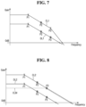
- FIGS. 5 to 8 are diagrams illustrating effects of a reception amplifier according to some example embodiments.
- FIG. 5 is a block diagram of a another example embodiment of an amplifier.
- FIG. 6 is a circuit diagram of FIG. 5 .
- FIG. 7 is a graph showing an example frequency response characteristic of the amplifier shown in FIGS. 5 and 6 .
- a feedforward circuit FFA 1 of an amplifier 99 does not receive a feedback signal VCMFB from a common-mode feedback circuit CFC.
- the feedback signal VCMFB which is an output from the common-mode feedback circuit CFC is not taken into consideration for the feedforward circuit FFA 1 of the amplifier 99 to perform feedforward control.
- the feedforward circuit FFA 1 of the amplifier 99 may only include a transistor MN 51 that is turned on by a bias voltage VBN to control a fixed current IF to flow into the feedforward circuit FFA 1 while the feedforward circuit FFA 1 is enabled.
- the frequency response characteristic of the amplifier 99 shows a gain difference between a common-mode loop CL 1 and a differential-mode loop DLL
- a pole P 2 is nulled by first and second Miller compensation circuits MCC 1 and MCC 2
- a pole P 3 is nulled by the feedforward circuit FFA 1 . Accordingly, the characteristic of a one-pole system can be achieved.
- the pole P 2 may be nulled by the first and second Miller compensation circuits MCC 1 and MCC 2 , but the pole P 3 is not nulled. Accordingly, there may be a problem such as the circuit oscillating due to the characteristic of a two-pole system having two poles.
- FIG. 8 is a graph showing a frequency response characteristic of the amplifier according to some example embodiments.
- the feedforward circuit FFA of the amplifier 100 receives the feedback signal VCMFB from the common-mode feedback circuit CFC and perform feedforward control on the basis of the feedback signal VCMFB. In other words, the feedforward circuit FFA of the amplifier 100 performs feedforward control in consideration of the feedback signal VCMFB which is the output from the common-mode feedback circuit CFC.
- the feedforward circuit FFA of the amplifier 100 includes the transistor MN 51 which is turned on by the bias voltage VBN to control the fixed current IF to flow into the feedforward circuit FFA while the feedforward circuit FFA is enabled and a transistor MN 52 which is turned on by the feedback signal VCMFB provided by the common-mode feedback circuit CFC to control the bias current IB to flow into the feedforward circuit FFA while the feedforward circuit FFA is enabled.
- a loop CLM of a new response characteristic is added to the frequency response characteristic of the amplifier, and thus a common-mode loop CL 2 can have the characteristic of a one-pole system.
- a pole P 2 is nulled by the first and second Miller compensation circuits MCC 1 and MCC 2
- a pole P 3 is nulled by the feedforward circuit FFA. Accordingly, the characteristic of a one-pole system can be achieved.
- the pole P 2 is nulled by the first and second Miller compensation circuits MCC 1 and MCC 2
- the pole P 3 is nulled by the feedforward circuit FFA which performs feedforward control on the basis of the feedback signal VCMFB provided by the common-mode feedback circuit CFC. Accordingly, the characteristic of a one-pole system can be achieved.
- the reception amplifier according to the some example embodiments has the characteristic of a one-pole system in both the differential-mode loop DL 2 and the common-mode loop CL 2 , and thus can stably operate.
- the sum of the sizes of the transistor MN 51 and the transistor MN 52 of the amplifier 100 according to the some example embodiments may be substantially the same as the size of the transistor 51 of the amplifier 99 .
- the transistor MN 51 of the amplifier 99 includes four unit transistors
- the transistor MN 51 of the amplifier 100 according to some example embodiments may include two unit transistors
- the transistor MN 52 may include two unit transistors.
- the transistor MN 51 of the amplifier 100 according to may include one unit transistor, and the transistor MN 52 may include three unit transistors, or the transistor MN 51 of the amplifier 100 may include three unit transistors, and the transistor MN 52 may include one unit transistor, etc.
- One or more of the elements disclosed above may include or be implemented in one or more processing circuitries such as hardware including logic circuits; a hardware/software combination such sa a processor executing software; or a combination thereof.
- the processing circuitries more specifically may include, but is not limited to, a central processing unit (CPU), an arithmetic logic unit (ALU), a digital signal processor, a microcomputer, a field programmable gate array (FGPA), a System-on-Chip (SoC), a programmable logic unit, a microprocessor, application-specific integrated circuit (ASIC), etc.
- CPU central processing unit
- ALU arithmetic logic unit
- FGPA field programmable gate array
- SoC System-on-Chip
- ASIC application-specific integrated circuit
- example embodiments of the inventive concepts have been described above with reference to the accompanying drawings, example embodiments are not limited thereto and can be manufactured in various different forms. It will be understood that example embodiments can be implemented in other specific, and the above-described example embodiments should be considered as illustrative rather than restrictive in all aspects.
Landscapes
- Engineering & Computer Science (AREA)
- Power Engineering (AREA)
- Computer Networks & Wireless Communication (AREA)
- Signal Processing (AREA)
- Microelectronics & Electronic Packaging (AREA)
- Amplifiers (AREA)
Abstract
Description
Claims (17)
Applications Claiming Priority (4)
| Application Number | Priority Date | Filing Date | Title |
|---|---|---|---|
| KR20210140288 | 2021-10-20 | ||
| KR10-2021-0140288 | 2021-10-20 | ||
| KR1020220048678A KR20230056559A (en) | 2021-10-20 | 2022-04-20 | Semiconductor device and communication device comprising the same |
| KR10-2022-0048678 | 2022-04-20 |
Publications (2)
| Publication Number | Publication Date |
|---|---|
| US20230117533A1 US20230117533A1 (en) | 2023-04-20 |
| US12308808B2 true US12308808B2 (en) | 2025-05-20 |
Family
ID=85982575
Family Applications (1)
| Application Number | Title | Priority Date | Filing Date |
|---|---|---|---|
| US17/881,734 Active 2043-07-31 US12308808B2 (en) | 2021-10-20 | 2022-08-05 | Semiconductor device and communication device including the same |
Country Status (3)
| Country | Link |
|---|---|
| US (1) | US12308808B2 (en) |
| CN (1) | CN115996029A (en) |
| TW (1) | TW202318815A (en) |
Families Citing this family (2)
| Publication number | Priority date | Publication date | Assignee | Title |
|---|---|---|---|---|
| TWI825698B (en) * | 2022-04-29 | 2023-12-11 | 瑞昱半導體股份有限公司 | Voltage regulator and signal amplifying circuit |
| TWI906025B (en) * | 2024-08-26 | 2025-11-21 | 達發科技股份有限公司 | Transconductance-transimpedance amplifier |
Citations (10)
| Publication number | Priority date | Publication date | Assignee | Title |
|---|---|---|---|---|
| US6329849B1 (en) | 1998-11-12 | 2001-12-11 | Kabushiki Kaisha Toshiba | Apparatus and method for converting differential voltage to fully balanced currents |
| US6573791B2 (en) | 2001-09-28 | 2003-06-03 | Koninklijke Philips Electronics N.V. | Multipath nested Gm nested miller compensation |
| US7453319B2 (en) | 2006-02-13 | 2008-11-18 | Texas Instruments Incorporated | Multi-path common mode feedback for high speed multi-stage amplifiers |
| US8319554B1 (en) | 2011-05-18 | 2012-11-27 | Texas Instruments Incorporated | Amplifier with start-up common mode feedback |
| US8963639B2 (en) | 2013-02-19 | 2015-02-24 | University Of Macau | Frequency compensation techniques for low-power and small-area multistage amplifiers |
| US20160308497A1 (en) * | 2015-04-20 | 2016-10-20 | Freescale Semiconductor, Inc. | Low drop out voltage regulator and method therefor |
| US9912311B2 (en) | 2015-07-22 | 2018-03-06 | Samsung Electronics Co., Ltd | Multimode reconfigurable amplifier and analog filter including the same |
| US10263568B2 (en) | 2017-02-23 | 2019-04-16 | Avaga Technologies International Sales PTE. Limited | Radio frequency feedback power amplifiers |
| US20190305739A1 (en) * | 2018-03-27 | 2019-10-03 | Samsung Electronics Co., Ltd. | Amplifying circuit including miller compensation circuit |
| US20220263479A1 (en) * | 2021-02-16 | 2022-08-18 | Qualcomm Incorporated | High gain-bandwidth product (gbw) amplifier with passive feedforward compensation |
-
2022
- 2022-08-05 US US17/881,734 patent/US12308808B2/en active Active
- 2022-10-07 TW TW111138108A patent/TW202318815A/en unknown
- 2022-10-18 CN CN202211272035.1A patent/CN115996029A/en active Pending
Patent Citations (12)
| Publication number | Priority date | Publication date | Assignee | Title |
|---|---|---|---|---|
| US6329849B1 (en) | 1998-11-12 | 2001-12-11 | Kabushiki Kaisha Toshiba | Apparatus and method for converting differential voltage to fully balanced currents |
| US6573791B2 (en) | 2001-09-28 | 2003-06-03 | Koninklijke Philips Electronics N.V. | Multipath nested Gm nested miller compensation |
| US7453319B2 (en) | 2006-02-13 | 2008-11-18 | Texas Instruments Incorporated | Multi-path common mode feedback for high speed multi-stage amplifiers |
| US8319554B1 (en) | 2011-05-18 | 2012-11-27 | Texas Instruments Incorporated | Amplifier with start-up common mode feedback |
| US8963639B2 (en) | 2013-02-19 | 2015-02-24 | University Of Macau | Frequency compensation techniques for low-power and small-area multistage amplifiers |
| US20160308497A1 (en) * | 2015-04-20 | 2016-10-20 | Freescale Semiconductor, Inc. | Low drop out voltage regulator and method therefor |
| US9553548B2 (en) | 2015-04-20 | 2017-01-24 | Nxp Usa, Inc. | Low drop out voltage regulator and method therefor |
| US9912311B2 (en) | 2015-07-22 | 2018-03-06 | Samsung Electronics Co., Ltd | Multimode reconfigurable amplifier and analog filter including the same |
| US10263568B2 (en) | 2017-02-23 | 2019-04-16 | Avaga Technologies International Sales PTE. Limited | Radio frequency feedback power amplifiers |
| US20190305739A1 (en) * | 2018-03-27 | 2019-10-03 | Samsung Electronics Co., Ltd. | Amplifying circuit including miller compensation circuit |
| US10797662B2 (en) | 2018-03-27 | 2020-10-06 | Samsung Electronics Co., Ltd. | Amplifying circuit including miller compensation circuit |
| US20220263479A1 (en) * | 2021-02-16 | 2022-08-18 | Qualcomm Incorporated | High gain-bandwidth product (gbw) amplifier with passive feedforward compensation |
Also Published As
| Publication number | Publication date |
|---|---|
| US20230117533A1 (en) | 2023-04-20 |
| TW202318815A (en) | 2023-05-01 |
| CN115996029A (en) | 2023-04-21 |
Similar Documents
| Publication | Publication Date | Title |
|---|---|---|
| US7948309B2 (en) | DC-offset cancelled programmable gain array for low-voltage wireless LAN system and method using the same | |
| CN110311629B (en) | Amplifier circuit including Miller compensation circuit | |
| US9184716B2 (en) | Low noise amplifier and receiver | |
| US8648652B2 (en) | Band pass filter and calibration method for band pass filter | |
| US9479120B2 (en) | Fully differential signal system including common mode feedback circuit | |
| US7420423B2 (en) | Active balun device | |
| US9166530B2 (en) | Low noise amplifier and receiver | |
| US20180323756A1 (en) | Power amplifier circuit with adjustable bias voltage | |
| CN103391049B (en) | The low-noise amplifier of gain adjustable | |
| US7129782B2 (en) | Fully differential amplifier with start up circuit | |
| US12308808B2 (en) | Semiconductor device and communication device including the same | |
| US20110163808A1 (en) | Amplifier with improved input resistance and controlled common mode | |
| US7215199B2 (en) | Method and system for simplifying common mode feedback circuitry in multi-stage operational amplifiers | |
| KR101127461B1 (en) | Highly Linear Variable Gain Amplifier | |
| EP2110947B1 (en) | Variable gain RF amplifier | |
| US8503966B2 (en) | Semiconductor integrated circuit and receiving apparatus | |
| US8884816B2 (en) | Temperature compensating device and satellite signal receiving system | |
| US7382175B2 (en) | Frequency mixer preventing degradation in linearity on amplitude of input signal | |
| US6429742B1 (en) | Gain-controlled tuned differential adder | |
| US6100763A (en) | Circuit for RF buffer and method of operation | |
| US9197176B2 (en) | Amplification device and transmitter | |
| GB2490977A (en) | A configurable LNA with inductive degeneration or with an impedance-matching stage in parallel with the principal gain stage | |
| US12424975B2 (en) | Semiconductor device and communication device comprising the same | |
| KR20230056559A (en) | Semiconductor device and communication device comprising the same | |
| US12095426B2 (en) | Amplifier and signal processing apparatus |
Legal Events
| Date | Code | Title | Description |
|---|---|---|---|
| FEPP | Fee payment procedure |
Free format text: ENTITY STATUS SET TO UNDISCOUNTED (ORIGINAL EVENT CODE: BIG.); ENTITY STATUS OF PATENT OWNER: LARGE ENTITY |
|
| AS | Assignment |
Owner name: SAMSUNG ELECTRONICS CO., LTD., KOREA, REPUBLIC OF Free format text: ASSIGNMENT OF ASSIGNORS INTEREST;ASSIGNORS:JOO, SEONG WON;GWEON, SU RIN;WOO, JEONG KYUN;SIGNING DATES FROM 20220802 TO 20220803;REEL/FRAME:060779/0009 |
|
| STPP | Information on status: patent application and granting procedure in general |
Free format text: DOCKETED NEW CASE - READY FOR EXAMINATION |
|
| AS | Assignment |
Owner name: SAMSUNG ELECTRONICS CO., LTD., KOREA, REPUBLIC OF Free format text: CORRECTIVE ASSIGNMENT TO CORRECT THE SECOND INVENTOR'S NAME PREVIOUSLY RECORDED AT REEL: 060779 FRAME: 0009. ASSIGNOR(S) HEREBY CONFIRMS THE ASSIGNMENT;ASSIGNORS:JOO, SEONG WON;GWEON, SURIN;WOO, JEONG KYUN;SIGNING DATES FROM 20220802 TO 20220913;REEL/FRAME:064365/0304 |
|
| STPP | Information on status: patent application and granting procedure in general |
Free format text: NON FINAL ACTION MAILED |
|
| STPP | Information on status: patent application and granting procedure in general |
Free format text: RESPONSE TO NON-FINAL OFFICE ACTION ENTERED AND FORWARDED TO EXAMINER |
|
| STPP | Information on status: patent application and granting procedure in general |
Free format text: NOTICE OF ALLOWANCE MAILED -- APPLICATION RECEIVED IN OFFICE OF PUBLICATIONS |
|
| STCF | Information on status: patent grant |
Free format text: PATENTED CASE |