US12237202B2 - Die bonding system with heated automatic collet changer - Google Patents
Die bonding system with heated automatic collet changer Download PDFInfo
- Publication number
- US12237202B2 US12237202B2 US17/421,270 US202017421270A US12237202B2 US 12237202 B2 US12237202 B2 US 12237202B2 US 202017421270 A US202017421270 A US 202017421270A US 12237202 B2 US12237202 B2 US 12237202B2
- Authority
- US
- United States
- Prior art keywords
- die
- tip
- heater
- heating apparatus
- wafer
- Prior art date
- Legal status (The legal status is an assumption and is not a legal conclusion. Google has not performed a legal analysis and makes no representation as to the accuracy of the status listed.)
- Active, expires
Links
Images


Classifications
-
- H01L21/68721—
-
- H—ELECTRICITY
- H10—SEMICONDUCTOR DEVICES; ELECTRIC SOLID-STATE DEVICES NOT OTHERWISE PROVIDED FOR
- H10P—GENERIC PROCESSES OR APPARATUS FOR THE MANUFACTURE OR TREATMENT OF DEVICES COVERED BY CLASS H10
- H10P72/00—Handling or holding of wafers, substrates or devices during manufacture or treatment thereof
- H10P72/70—Handling or holding of wafers, substrates or devices during manufacture or treatment thereof for supporting or gripping
- H10P72/76—Handling or holding of wafers, substrates or devices during manufacture or treatment thereof for supporting or gripping using mechanical means, e.g. clamps or pinches
- H10P72/7604—Handling or holding of wafers, substrates or devices during manufacture or treatment thereof for supporting or gripping using mechanical means, e.g. clamps or pinches the wafers being placed on a susceptor, stage or support
- H10P72/7606—Handling or holding of wafers, substrates or devices during manufacture or treatment thereof for supporting or gripping using mechanical means, e.g. clamps or pinches the wafers being placed on a susceptor, stage or support characterised by edge clamping, e.g. clamping ring
-
- H01L21/67132—
-
- H01L21/67144—
-
- H—ELECTRICITY
- H10—SEMICONDUCTOR DEVICES; ELECTRIC SOLID-STATE DEVICES NOT OTHERWISE PROVIDED FOR
- H10P—GENERIC PROCESSES OR APPARATUS FOR THE MANUFACTURE OR TREATMENT OF DEVICES COVERED BY CLASS H10
- H10P72/00—Handling or holding of wafers, substrates or devices during manufacture or treatment thereof
- H10P72/04—Apparatus for manufacture or treatment
- H10P72/0442—Apparatus for placing on an insulating substrate, e.g. tape
-
- H—ELECTRICITY
- H10—SEMICONDUCTOR DEVICES; ELECTRIC SOLID-STATE DEVICES NOT OTHERWISE PROVIDED FOR
- H10P—GENERIC PROCESSES OR APPARATUS FOR THE MANUFACTURE OR TREATMENT OF DEVICES COVERED BY CLASS H10
- H10P72/00—Handling or holding of wafers, substrates or devices during manufacture or treatment thereof
- H10P72/04—Apparatus for manufacture or treatment
- H10P72/0446—Apparatus for mounting on conductive members, e.g. leadframes or conductors on insulating substrates
Definitions
- the bond head heat the die, as opposed to the substrate, to reflow temperatures, so as to not impact any previously-attached neighboring die(s).
- focused energy sources e.g. a laser
- focused energy sources if relied upon to provide too much heat, can cause cracking of the substrate, thereby ruining it.
- Heated bond heads to date have been typically designed for dedicated applications i.e. the bond heads are specific to a die size and designed to hold a steady temperature.
- the heated bond heads typically do not have the capability to ramp their temperature up or down quickly or to accommodate different die sizes.
- heated bond heads when picking dies from commonly used input devices (e.g. waffle-packs, gel-packs, and wafers) need to be cooled down to ⁇ 50° C., since the input devices are plastic trays or films and cannot handle higher temperatures.
- input devices e.g. waffle-packs, gel-packs, and wafers
- an error budget is typically created.
- This error budget is generally broken into various categories, such as motion error in the gantry, imaging error, system calibration error, error introduced during picking of the die, and error introduced while placing a die on the substrate.
- These errors can be minimized using well-established methods, such as a high-performance gantry system, high-quality imaging optics and illumination, and keeping the system in a temperature-stable environment to maintain system calibration.
- a ‘pick’ error is inevitably introduced.
- One way to minimize pick error is to use a stationary up-facing camera that is located in the gantry work area, but mounted on the machine deck at a specific location.
- the stationary camera images die fiducials, which are positioned on the bottom of the die, and calculates the ‘pick’ error.
- the pick error is then accounted for by the gantry system when the die is placed on its final location. While this is generally effective, it is not without its challenges and limitations.
- the location of the stationary up-facing camera mounted on the machine deck has to be calibrated precisely for high precision bonding.
- any changes in the ambient temperature or that of the gantry which is typically due to heat generated by its motors, affects the calibration of the up-facing camera and is sometimes referred to as drift.
- a die bonding system comprising a heated bond head with the ability to heat up and cool down quickly, change tips, which may herein be referred to as end effectors, to handle different sized dies, and load and unload tips automatically while maintaining the precision required for handling dies smaller than ⁇ 200 um 2 .
- the die bonding system in embodiments, further comprises a wafer handler that rests on cams, which allow the rapid planarization thereof to a die bond head and do not require re-planarization between subsequent die bonding operations using the same wafer.
- the die bonding system also comprises a substrate heater that functions to heat the wafer from below using a contact heater that substantially encircles an area in which a die is to be bonded, allowing it to be pre-heated before a focused energy source, such as a laser, is aimed therethrough to supply the additional heat necessary to carry out the die bonding operation, thereby minimizing the chance of wafer cracking and misalignment.
- a focused energy source such as a laser
- FIG. 1 is an isometric view of a cam-adjustable wafer table and wafer pre-heater, in accordance with embodiments of the present disclosure
- FIG. 2 is an isometric view of a cam-adjustable wafer table, wafer pre-heater, and focused energy source, in accordance with embodiments of the present disclosure
- FIG. 4 is a section view of a cam-adjustable wafer table having a wafer support structure and focused energy source, in accordance with embodiments of the present disclosure
- FIG. 5 is a section view of a cam-adjustable wafer table, wafer pre-heater, and focused energy source, in accordance with embodiments of the present disclosure
- FIG. 6 is an isometric view of a cam-adjustable wafer table and focused energy source that further includes a near-field camera in a retracted position, in accordance with embodiments of the present disclosure
- FIG. 7 is a side elevation view of a cam-adjustable wafer table and focused energy source that further includes a near-field camera in a retracted position, in accordance with embodiments of the present disclosure
- FIG. 8 is an isometric view of a cam-adjustable wafer table and focused energy source that further includes a near-field camera in an extended position, in accordance with embodiments of the present disclosure
- FIG. 9 is a side elevation view of a cam-adjustable wafer table and focused energy source that further includes a near-field camera in an extended position, in accordance with embodiments of the present disclosure
- FIG. 10 is a perspective view showing a heated bond head with no tip or end effector, where the heater power leads and cooling port are identified, configured in accordance with embodiments of the present disclosure
- FIG. 11 is a perspective view showing a tip or end effector, configured in accordance with embodiments of the present disclosure.
- FIG. 12 is a perspective view of the heated bond head with no tip or end effector of FIG. 10 connected to a die bond head, in accordance with embodiments of the present disclosure
- FIG. 13 is a perspective view of the heated bond head of FIG. 10 with the tip or end effector of FIG. 11 connected thereto and the entire assembly connected to a die bond head, in accordance with embodiments of the present disclosure;
- FIG. 14 is a side elevation view of the heated bond head of FIG. 10 with the tip or end effector of FIG. 11 connected thereto and the entire assembly connected to a die bond head, in accordance with embodiments of the present disclosure;
- FIG. 15 is a perspective view showing a die bond head positioned above a machine deck having a plurality of pockets configured to retain tips or end effectors in a nominal XYZT location, one pocket containing a tip or end effector, configured in accordance with embodiments of the present disclosure;
- FIG. 16 is a perspective view showing a die bond head positioned just above a machine deck having a plurality of pockets configured to retain tips or end effectors in a nominal XYZT location, some pocket containing a tip or end effector, the die bond head depicted picking up a tip or end effector from a pocket of the machine deck, in accordance with embodiments of the present disclosure;
- FIG. 17 is a side elevation view showing a die bond head positioned just above a machine deck having a plurality of pockets configured to retain tips or end effectors in a nominal XYZT location, some pocket containing a tip or end effector, the die bond head depicted picking up a tip or end effector from a pocket of the machine deck, in accordance with embodiments of the present disclosure.
- the X, Y, and Z axis should be understood to refer to the three orthogonal linear axes while “T”, which may also be referred to as Theta or ⁇ , refers to a revolute axis.
- the term “cammed”, when used in reference to a wafer handler 100 should be understood to refer to a wafer handler 100 that is able to manipulate the roll, pitch, and yaw of a wafer 300 to achieve planarization.
- Z-axis motion of the wafer handler 100 is still present.
- the wafer handler 100 may be cammed, but restricted to Z-axis motion, in embodiments by synchronizing all cams 106 .
- FIGS. 1 - 9 show a cam-adjustable, or cammed, wafer handler 100 that maximizes efficiency, while ensuring planarity of a wafer 300 to a die bond head 1200 , by requiring only one alignment procedure to be performed per-wafer 300 , assuming that a single tip 1100 , which may also be herein referred to as an end effector 1100 , is used to bond dies thereto (in embodiments, an alignment procedure must be performed after a tip 100 change as well).
- the cammed wafer handler 100 utilizes three motors 102 , with each motor 102 distributed evenly around the wafer handler 100 and having a cam 106 affixed thereto, the cams 106 each resting on a separate pedestal 104 that is connected to the wafer handler 100 , providing for fine alignment of a die bond head 1200 to a wafer 300 . More specifically, such embodiments allow for precise control over the roll, pitch, and yaw of a wafer 300 mounted on the wafer handler 100 , allowing the planarity of the wafer 300 to be precisely matched with a die-to-be-bonded.
- a die-to-be-bonded is suspended above the wafer by a die bond head 1200 to which a heater 1000 and removable tip 1100 are affixed.
- the die bond head 1200 is itself disposed on an overhead gantry to allow for gross positioning thereof.
- three distance sensors are used to planarize a wafer 300 to the die bond head 1200 , one of which is used to profile the wafer 300 .
- a flat vacuum platen is used to secure a wafer 300 to the cammed wafer handler 100 .
- the motors 102 are stepper motors.
- FIGS. 3 - 9 show the cammed wafer handler 100 of FIGS. 1 - 2 with a flat vacuum platen mounted thereon.
- the flat vacuum platen in embodiments, comprises vacuum passages disposed about an upper surface thereof that are connected to a vacuum source disposed on a die bond system of which the wafer handler 100 is a part, allowing a wafer 300 to be held tightly and flatly against the wafer handler 100 , enabling a high degree of die bonding accuracy.
- the wafer handler 100 is used in one of three general ways.
- a cammed wafer handler 100 planarizes to the bottom of a die and/or tip 1100 , which may be removable, via sensor feedback on one or both surfaces.
- a wafer pre-heater 108 such as that depicted in FIGS. 1 , 2 , and 5 , is used to planarize local areas on the wafer. No wafer 300 camming is necessary in such embodiments, as the wafer pre-heater 108 of such embodiments is permanently planarized with respect to bottom of tips 1100 , which may be removable, on a die bond head 1200 .
- a gimballing tip 1100 is used with a non-cammed wafer handler 100 for die placement.
- FIG. 1 an isometric view of a cam-adjustable wafer handler 100 , which may also be herein referred to as a wafer table 100 , and wafer pre-heater 108 are shown.
- the embodiment shown in FIG. 1 comprises three motors 102 , each connected to a cam 106 comprising a cam lobe 106 configured to make sliding contact with a separate wafer table projection 104 while rotating, thereby imparting variable motion to the wafer table 100 via the wafer table projections 104 .
- the roll, pitch, and yaw of the wafer table 100 and any wafer 300 mounted thereto can be manipulated to achieve planarization.
- Z-axis motion of the wafer table 100 can be accomplished.
- FIG. 1 also shows a wafer pre-heater 108 , in accordance with embodiments of the present disclosure.
- the wafer pre-heater 108 comprises a pedestal portion 110 and a base 112 that, in embodiments, is mounted to a movable platform to permit the alignment thereof to a particular region of the wafer table 100 and a wafer 300 mounted thereon.
- the wafer pre-heater 108 may be used to both heat and locally planarize a wafer 300 .
- the wafer pre-heater 108 is permanently planarized with respect to a tip 1100 configured to hold a die-to-be-bonded.
- the wafer pre-heater 108 comprises a hollow central section configured to allow a focused energy source 200 to be transmitted therethrough.
- the wafer pre-heater 108 alone is used for both heating and planarization.
- such a planarization system and method may be combined with a cammed wafer frame 100 , which, in embodiments, through synchronized movement of cams 106 , is only used as a Z-axis positioner to remove and attach a wafer 300 to the wafer pre-heater 108 .
- the cammed wafer handler 100 may be positioned just below a wafer-contacting portion of the wafer pre-heater 108 , allowing the cammed wafer handler 100 to limit the sag of wafer 300 edges, thereby reducing stress on the wafer 300 during a bonding operation.
- the wafer 300 itself is movable, while the wafer pre-heater 108 remains stationary. In still other embodiments, the wafer 300 is capable of gross movement in the X and Y directions and limited movement in the Z direction while the wafer pre-heater 108 is capable of movement in the Z direction only.
- the wafer pre-heater in embodiments, includes a heater 108 , in embodiments a circular heater 108 , disposed at a tip thereof, i.e. the end furthest from the mounting base 112 that is separated therefrom by a pedestal 110 .
- the heater 108 is, in embodiments, thermally isolated from the remainder thereof and die bonding system generally by a thermal insulator, in embodiments, a ceramic disk.
- the wafer pre-heater 108 in embodiments, further comprises a hollow central section that is in communication with a focused energy source 200 , such as a laser 200 , that is of sufficient power to complete a die bonding operation.
- the heater 108 located at the tip of the wafer pre-heater 108 functions to preheat a portion of a wafer 300 to a temperature sufficient to minimize the energy required from the focused energy source 200 to complete a die bonding operation, thereby reducing the chances of wafer 300 cracking, thereby improving yield while ensuring a strong bond.
- FIGS. 10 - 14 show an additional design for a heater, a die heater 1000 , in accordance with embodiments of the present disclosure.
- the die heater 1000 shown in FIGS. 10 - 14 utilizes a plurality of rods 1004 or pins 1004 that are evenly and concentrically disposed about a central axis of the die heater 1000 and act as a standoff for the die heater 1004 .
- the rods 1004 serve as a flexure mount, allowing for repeatable thermal expansion and contraction characteristics that enable sub-micron accuracy, since thermal expansion and contraction result in the central axis of the die heater 1000 precisely returning to its set point following each thermal cycle.
- the use of rods 1004 helps to isolate the die heater 1000 from a remainder of a die bonding system, reducing parasitic heat loss thereto while minimizing thermal expansion and contraction thereof due to heat conduction to or from the die heater 1000 .
- the die heater 1000 is cooled by forced air cooling.
- a die bonding system to which the die heater is attached, during use provides the forced air for cooling.
- the cooling air is directed against a backside of the die heater 1000 using a nozzle to focus the air thereon.
- rods 1004 are retained in a die bonding system through the use of jaws, set screws, or other suitable retaining means, as would be known to one of ordinary skill in the art.
- the heater embodiment shown in FIGS. 10 - 14 also comprises a trough 1008 comprising a vacuum port 1006 surrounding a circular central projection 1012 which itself, in embodiments, comprises a second, centrally-located vacuum port 1010 .
- the trough 1008 is configured, in embodiments, to retain removable tips 1100 , which can also be considered adapters 1100 that allow the die heater 1004 to pick and place a variety of dies and to accommodate a variety of mounting locations (e.g. deep wells that require a slim die-holding extension), through the use of a vacuum drawn through the vacuum port 1006 .
- the second, centrally-located vacuum port 1010 of embodiments is used, in embodiments, to provide vacuum to a tip 1100 that, in embodiments, passes that vacuum through connector 1102 , providing for secure retaining of a die or dies thereon.
- the removable tips 1100 comprise a connector 1102 configured to allow for connection between the removal tip 1100 and a die to be bonded.
- the connector 1102 provides for the communication of electricity, vacuum, and/or information between the die heater 1000 and removable tip 1100 and/or die retained thereby.
- the connector 1102 provides for the selective communication of vacuum between the die heater 1000 and removable tip 1100 , allowing a die or dies to be selectively retained thereby.
- the removable tips 1100 comprise at least one alignment feature 1104 that, in embodiments, is used to obtain rough alignment of the tip 1100 , in embodiments by interfacing with a dowel 1504 located in at least one pocket of the machine deck 1500 .
- the removable tips 1100 comprise at least two alignment apertures 1106 that, in embodiments, are used in conjunction with at least one near-field camera assembly 600 as fiducials to obtain fine alignment. In embodiments, the removable tips 1100 comprise three such alignment apertures 1106 .
- the central projection 1012 is non-circular, allowing rotation of the removable tips 1100 to be constrained more than friction alone would allow.
- the central projection 1012 is of the same height as the remainder of the die heater 1004 , with the exception of the aforementioned trough 1008 .
- the tips 1100 are configured to gimbal, in embodiments using a gantry-mounted gimbal. Such embodiments are suitable for use with non-cammed wafer handlers 100 .
- a non-heated, gimballing tip 1100 may also be used with non-cammed wafer handlers 100 .
- non-gimballing, non-heated tips may be used with cammed wafer handlers 100 , such as those depicted in FIGS. 1 - 9 and described in the following paragraphs.
- non-gimballing, heated tips 1100 may be used with cammed wafer handlers 100 .
- FIGS. 12 - 14 Alternative embodiments of the die heater 1000 shown in FIG. 10 are shown in FIGS. 12 - 14 , where the die heater 1000 is attached to a a die bond head 1200 that is, in embodiments, connected to a gantry (not depicted in figures).
- the heater design shown in these figures allows for enhanced mechanical repeatability, which allows more accurate placement of dies, faster heating and cooling, due to the absence of mass from the die heater 1000 support and constraint surfaces, relatively simple planarity mirroring, and minimizes heat conduction to the larger system, due, in part, to the thermal isolating effects of the pin 1004 support system thereof.
- the heater comprises at least two vacuum connections 1002 .
- the first vacuum connection 1002 connects a vacuum source to an orifice 1006 disposed in the aforementioned trough 1008 , which is configured to accept a removable tip configured to fit therein, allowing the removable tip 1100 to be selectively retained. This configuration allows the removable tip 1100 to be easily replaced to allow the bonding of a different die or to allow for bonding to occur in a location requiring a different removable tip 1100 .
- the second vacuum connection 1002 connects a vacuum source, which may be the same or a different vacuum source, to a central orifice 1010 of the die heater 1000 .
- removable tips 1100 configured for use with this die heater 1000 comprise an orifice 1102 adjacent a die-retaining area located opposite the die heater 1000 that connects to this central orifice 1010 , allowing vacuum to be applied therethrough, thereby allowing for the selective retaining (i.e. pick and place functionality) of a die to be bonded.
- the aforementioned rods 1004 are electrical studs 1004 or pins 1004 that serve a dual purpose, namely fixing the die heater 1000 to the remainder of a die-bonding system and supplying power and ground to the die heater 1004 .
- the aforementioned rods 1004 may serve only to fix the die heater 1000 to the remainder of a die-bonding system.
- six rods 1004 are used, although greater or fewer rods 1004 could be used without departing from the teachings of the present disclosure.
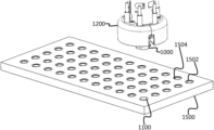
- FIGS. 15 - 17 a machine deck 1500 having a plurality of pockets 1502 configured to retain tips 1100 in a nominal XYZT location is shown.
- the machine deck 1500 having a plurality of pockets 1502 configured to retain tips 1100 in a nominal XYZT location is shown accompanied by a die bond head 1200 in the process of picking up a tip 1100 .
- machine vision techniques are used to align the die bond head 1200 and tip 1100 to ensure sufficient accuracy.
- the combination of an up-look and down-look camera is used to align the die bond head 1200 and tip 1100 .
- the cameras may be configured to have a relatively shallow depth of field and achieve depth control through focus.
- Such a camera system may be referred to as a near field optics assembly 600 and may also be used to ensure minimal placement error when configured such that one camera looks up towards a die to be bonded when positioned over a gantry work area and a second camera is positioned to look down towards a substrate (e.g. a wafer) in the vicinity of a die bonding location, as in various embodiments of the present disclosure.
- a substrate e.g. a wafer
- the near-field optics system 600 is much the same, regardless of whether its concepts are applied to die bond head 1200 /tip 1100 alignment or to die to substrate alignment, the system, as discussed below, should be understood to be useful in either context, even where it is described specifically in only one or the other.
- a near field optics assembly 600 comprises a pair of cameras, optics, and sources of illumination.
- One camera is configured to look up at die fiducials (or the die bond head 1200 ) while the other looks down on corresponding substrate fiducials near which the die is to be placed (or on tips 1100 to be secured to the die bond head 1200 ).
- a die is picked and presented at a nominal XYTheta place location, but with a sufficient ‘Z’ separation to introduce the near field optics assembly 600 .
- the near field optics assembly 600 is mounted on a high precision, suspended XY gantry device. With the die and substrate stationary, the near field optics assembly 600 is introduced between the two and images a pair (or more) of die fiducials and corresponding substrate fiducials. The error between ideal die and substrate alignment is then calculated before retracting the near field optics assembly 600 . The gantry is then commanded to make the delta motion in XYT before moving in Z to place a die at its final location.
- the near field optics assembly 600 calibration needs to be stable for the machine performance to be stable.
- the near field optics assembly 600 is susceptible to thermal drifts if the environment changes or if heat is introduced by the process, or machine elements (e.g. heating elements). Putting the entire machine in a thermally stable environment may not accomplish this goal, since there is no good way of controlling the machine elements without limiting the machine utility and/or cycle time, since they are actively used in the process the machine runs. For these reasons, it has been found that it is better to thermally control the precision alignment apparatus (i.e. near field alignment optics assembly 600 ) than the entire machine or put limits on the machine elements. With a stable near field optics assembly 600 , especially one that is relatively small in mass and size relative to the entire machine, the machine calibration becomes less critical.
- a more efficient way of achieving temperature stability is to water cool the near field optics assembly 600 .
- this is accomplished using an external chiller, which cools water in a reservoir to a stable temperature.
- the water is then pumped into the near field optics assembly 600 , which comprises machined channels for the water to flow through.
- the ‘warmer’ water is circulated back into the reservoir where it mixes with the cooler water.
- the chiller operates continuously when the machine is turned off, idle or running, keeping the near field optics assembly 600 at a stable temperature setting at all times. If calibrated following temperature stabilization, as is done in embodiments, the machine stays in specification regardless of the process that the user runs on the machine or changes in ambient conditions.
- FIG. 16 a view of the machine deck 1500 of FIG. 15 having a plurality of pockets 1502 configured to retain tips 1100 in a nominal XYZT location, the pockets 1502 each containing a tip 1100 , is shown with a die heater 1000 connected to a die bond head 1200 picking up a tip 1100 for use.
- the outer vacuum ports 1002 of the die heater 1000 are used to secure a tip 1100 to the die heater 1000 using vacuum port 1006 and to secure a die to the tip 1100 using central vacuum ports 1010 / 1102 , allowing for the controlled pick and release of a component or die.
- the central port 1102 also acts as a locating pin, allowing the tip 1100 to expand without effecting die or component placement accuracy.
- the central vacuum port 1102 of the tip 1100 is chamfered to allow for at least partial self-locating between tip 1100 and die.
- the die heater 1000 is made with Aluminum Nitride (AlN) or similar ceramic material for fast thermal response and high thermal stability.
- AlN Aluminum Nitride
- the die heater 1000 and tip 1100 are capable of being heated to high temperatures, in embodiments ⁇ 450° C.
- non-heated tips 1100 are used.
- non-heated dies having an extension for positioning dies within narrow cavities are used in conjunction with the die heater 1000 .
- non-heated tips are made of Stainless Steel (SS) while, in other embodiments, non-heated tips are made of Tungsten Carbide (WC).
- outer vacuum ports 1002 of the die heater 1000 are used to provide vacuum to secure tips 1100 through vacuum port 1006 while the centrally-located vacuum port 1010 is used to provide vacuum to secure a die or other component the tip 1100 is designed to place thereto.
- the tip 1100 comprises a cavity connecting the central vacuum port 1102 used to secure a die or other component to a region of the tip 1100 configured to interface with the die or component (e.g. central vacuum port 1102 ) through central vacuum port 1102 .
- coolant is introduced into heaters to rapidly cool them and any attached tip 1100 , speeding cycle times.
- multiple cooling ports are used.
- gaseous, liquid, solid, and phase change cooling mediums are utilized as coolant.
- air or nitrogen is used as a coolant, dependent on the specific application. Coolant may also be injected into a ceramic matrix, thereby containing the coolant, or simply allowed to disperse after being introduced to the die heater 1000 .
- thermocouple which may be a type K thermocouple, is used to measure the temperature of the die heater 1000 .
- wires contained within the heater power leads 1004 are coated in Polytetrafluoroethylene (PTFE).
- the tip 1100 is made of MN to provide fast thermal response.
- the tip 1100 is made of Copper Tungsten (CuW), which provides heat-resistance, ablation-resistance, high thermal and electrical conductivity, and is easy to machine.
- the tip 1100 is made of Tungsten Carbide (WC).
- the central aperture of the tip 1100 is configured to connect a vacuum port 1006 of the die heater 1000 , which allows for releasably and controllably securing a die or component to the tip 1100 , to the portion of the tip 1100 on which a die is configured to be held.
- the die-holding portion of the tip 1100 is a pedestal 1102 while, in other embodiments, it is a flat portion adjacent a conical portion of the tip 1100 .
- the precise shapes, thicknesses, and configurations vary, in embodiments, to accommodate the dimensions of a substrate on which a die or component is to be placed.
- a non-heated tip 1100 comprises a neck portion and a conical shaped tip 1100 is shown.
- the flat portion of the region adjacent the conical region in embodiments, contains an aperture connecting the vacuum port 1006 of the die heater 1000 thereto, allowing for the controlled picking and releasing of a die or component.
- the neck portion of this embodiment allows the die to be placed within a cavity in the substrate.
- the die heater comprises heater power and thermocouple leads, cooling air exhaust, cooling air inlet, and ceramic insulator with channels for air cooling.
Landscapes
- Wire Bonding (AREA)
- Die Bonding (AREA)
Abstract
Description
Claims (16)
Priority Applications (1)
| Application Number | Priority Date | Filing Date | Title |
|---|---|---|---|
| US17/421,270 US12237202B2 (en) | 2019-03-18 | 2020-03-18 | Die bonding system with heated automatic collet changer |
Applications Claiming Priority (3)
| Application Number | Priority Date | Filing Date | Title |
|---|---|---|---|
| US201962819996P | 2019-03-18 | 2019-03-18 | |
| US17/421,270 US12237202B2 (en) | 2019-03-18 | 2020-03-18 | Die bonding system with heated automatic collet changer |
| PCT/US2020/023252 WO2020190991A1 (en) | 2019-03-18 | 2020-03-18 | Die bonding system with heated automatic collet changer |
Publications (2)
| Publication Number | Publication Date |
|---|---|
| US20220102187A1 US20220102187A1 (en) | 2022-03-31 |
| US12237202B2 true US12237202B2 (en) | 2025-02-25 |
Family
ID=72520487
Family Applications (1)
| Application Number | Title | Priority Date | Filing Date |
|---|---|---|---|
| US17/421,270 Active 2042-06-20 US12237202B2 (en) | 2019-03-18 | 2020-03-18 | Die bonding system with heated automatic collet changer |
Country Status (4)
| Country | Link |
|---|---|
| US (1) | US12237202B2 (en) |
| CN (1) | CN113544834A (en) |
| SG (1) | SG11202108016VA (en) |
| WO (1) | WO2020190991A1 (en) |
Citations (21)
| Publication number | Priority date | Publication date | Assignee | Title |
|---|---|---|---|---|
| JPS5928351A (en) * | 1982-08-10 | 1984-02-15 | Toshiba Corp | Bonding device |
| US6010056A (en) * | 1997-06-18 | 2000-01-04 | Swanson; David W. | Gimbal horn pressure head with shape of pivot rod bearing corresponding to shape of contact surface |
| JP2004047692A (en) * | 2002-07-11 | 2004-02-12 | Mitsubishi Electric Corp | Electronic component manufacturing apparatus and electronic component manufacturing method |
| US20070181644A1 (en) * | 2004-06-08 | 2007-08-09 | Matsushita Electric Industrial Co., Ltd. | Component mounting method and component mounting apparatus |
| KR20080042583A (en) | 2006-11-10 | 2008-05-15 | 주식회사 에이디피엔지니어링 | Lift pin driving device and flat panel display device manufacturing device having the same |
| US20080233680A1 (en) * | 2007-03-24 | 2008-09-25 | Dan Okamoto | Semiconductor Die Collet and Method |
| US20080295970A1 (en) | 2002-12-09 | 2008-12-04 | Ali Afzali-Ardakani | System and method of transfer printing an organic semiconductor |
| US20090126188A1 (en) * | 2005-06-20 | 2009-05-21 | Tadahiko Sakai | Electronic component thermo-compression tool, and electronic component mounting apparatus and mounting method |
| US20100083494A1 (en) * | 2003-12-31 | 2010-04-08 | Chippac, Inc. | Bonding Tool for Mounting Semiconductor Chips |
| US20120267423A1 (en) * | 2011-04-19 | 2012-10-25 | Taiwan Semiconductor Manufacturing Company, Ltd. | Methods and Apparatus for Thin Die Processing |
| US20140154037A1 (en) | 2011-06-03 | 2014-06-05 | Orion Systems Integration Pte Ltd | Method and systems for semiconductor chip pick & transfer and bonding |
| US20150129135A1 (en) | 2013-11-13 | 2015-05-14 | Semes Co., Ltd. | Bonding head and die bonding apparatus having the same |
| US20150173209A1 (en) * | 2013-12-18 | 2015-06-18 | Hemanth Dhavaleswarapu | Thermal compression bonding process cooling manifold |
| US9373530B2 (en) * | 2009-09-09 | 2016-06-21 | Kulicke And Soffa Die Bonding Gmbh | Tool for picking a planar object from a supply station |
| JP2016157885A (en) | 2015-02-26 | 2016-09-01 | キヤノン株式会社 | Semiconductor mounting device, ink jet head device and semiconductor component manufacturing method |
| US20170154804A1 (en) | 2015-12-01 | 2017-06-01 | Lam Research Corporation | Control of the incidence angle of an ion beam on a substrate |
| US20180114767A1 (en) * | 2016-10-25 | 2018-04-26 | Kulicke And Soffa Industries, Inc. | Bond head assemblies including reflective optical elements, related bonding machines, and related methods |
| US10861819B1 (en) * | 2019-07-05 | 2020-12-08 | Asm Technology Singapore Pte Ltd | High-precision bond head positioning method and apparatus |
| US20220336281A1 (en) * | 2019-09-06 | 2022-10-20 | Showa Denko Materials Co., Ltd. | Method of manufacturing semiconductor device and collet |
| US20230031977A1 (en) * | 2021-07-28 | 2023-02-02 | Disco Corporation | Chip conveying apparatus and die bonder |
| US20230317676A1 (en) * | 2022-04-01 | 2023-10-05 | Intel Corporation | Bond head design for thermal compression bonding |
Family Cites Families (4)
| Publication number | Priority date | Publication date | Assignee | Title |
|---|---|---|---|---|
| WO2001095379A1 (en) * | 2000-06-02 | 2001-12-13 | Ibiden Co., Ltd. | Hot plate unit |
| JP2006324549A (en) * | 2005-05-20 | 2006-11-30 | Sony Corp | Element transfer device, element transfer method, and display device manufacturing method |
| US9484241B2 (en) * | 2013-07-29 | 2016-11-01 | Asm Technology Singapore Pte Ltd | Device for holding multiple semiconductor devices during thermocompression bonding and method of bonding |
| US20180248090A1 (en) * | 2017-02-27 | 2018-08-30 | Rohinni, LLC | Semiconductor Device Circuit Apparatus Bonded with Anisotropic Conductive Film and Method of Direct Transfer for Making the Same |
-
2020
- 2020-03-18 CN CN202080015756.7A patent/CN113544834A/en active Pending
- 2020-03-18 US US17/421,270 patent/US12237202B2/en active Active
- 2020-03-18 SG SG11202108016V patent/SG11202108016VA/en unknown
- 2020-03-18 WO PCT/US2020/023252 patent/WO2020190991A1/en not_active Ceased
Patent Citations (21)
| Publication number | Priority date | Publication date | Assignee | Title |
|---|---|---|---|---|
| JPS5928351A (en) * | 1982-08-10 | 1984-02-15 | Toshiba Corp | Bonding device |
| US6010056A (en) * | 1997-06-18 | 2000-01-04 | Swanson; David W. | Gimbal horn pressure head with shape of pivot rod bearing corresponding to shape of contact surface |
| JP2004047692A (en) * | 2002-07-11 | 2004-02-12 | Mitsubishi Electric Corp | Electronic component manufacturing apparatus and electronic component manufacturing method |
| US20080295970A1 (en) | 2002-12-09 | 2008-12-04 | Ali Afzali-Ardakani | System and method of transfer printing an organic semiconductor |
| US20100083494A1 (en) * | 2003-12-31 | 2010-04-08 | Chippac, Inc. | Bonding Tool for Mounting Semiconductor Chips |
| US20070181644A1 (en) * | 2004-06-08 | 2007-08-09 | Matsushita Electric Industrial Co., Ltd. | Component mounting method and component mounting apparatus |
| US20090126188A1 (en) * | 2005-06-20 | 2009-05-21 | Tadahiko Sakai | Electronic component thermo-compression tool, and electronic component mounting apparatus and mounting method |
| KR20080042583A (en) | 2006-11-10 | 2008-05-15 | 주식회사 에이디피엔지니어링 | Lift pin driving device and flat panel display device manufacturing device having the same |
| US20080233680A1 (en) * | 2007-03-24 | 2008-09-25 | Dan Okamoto | Semiconductor Die Collet and Method |
| US9373530B2 (en) * | 2009-09-09 | 2016-06-21 | Kulicke And Soffa Die Bonding Gmbh | Tool for picking a planar object from a supply station |
| US20120267423A1 (en) * | 2011-04-19 | 2012-10-25 | Taiwan Semiconductor Manufacturing Company, Ltd. | Methods and Apparatus for Thin Die Processing |
| US20140154037A1 (en) | 2011-06-03 | 2014-06-05 | Orion Systems Integration Pte Ltd | Method and systems for semiconductor chip pick & transfer and bonding |
| US20150129135A1 (en) | 2013-11-13 | 2015-05-14 | Semes Co., Ltd. | Bonding head and die bonding apparatus having the same |
| US20150173209A1 (en) * | 2013-12-18 | 2015-06-18 | Hemanth Dhavaleswarapu | Thermal compression bonding process cooling manifold |
| JP2016157885A (en) | 2015-02-26 | 2016-09-01 | キヤノン株式会社 | Semiconductor mounting device, ink jet head device and semiconductor component manufacturing method |
| US20170154804A1 (en) | 2015-12-01 | 2017-06-01 | Lam Research Corporation | Control of the incidence angle of an ion beam on a substrate |
| US20180114767A1 (en) * | 2016-10-25 | 2018-04-26 | Kulicke And Soffa Industries, Inc. | Bond head assemblies including reflective optical elements, related bonding machines, and related methods |
| US10861819B1 (en) * | 2019-07-05 | 2020-12-08 | Asm Technology Singapore Pte Ltd | High-precision bond head positioning method and apparatus |
| US20220336281A1 (en) * | 2019-09-06 | 2022-10-20 | Showa Denko Materials Co., Ltd. | Method of manufacturing semiconductor device and collet |
| US20230031977A1 (en) * | 2021-07-28 | 2023-02-02 | Disco Corporation | Chip conveying apparatus and die bonder |
| US20230317676A1 (en) * | 2022-04-01 | 2023-10-05 | Intel Corporation | Bond head design for thermal compression bonding |
Non-Patent Citations (1)
| Title |
|---|
| International Preliminary Report on Patentability for PCT Appl. No. PCT/US2020/023252 dated Sep. 30, 2021, 9 Pages. |
Also Published As
| Publication number | Publication date |
|---|---|
| CN113544834A (en) | 2021-10-22 |
| US20220102187A1 (en) | 2022-03-31 |
| WO2020190991A1 (en) | 2020-09-24 |
| SG11202108016VA (en) | 2021-10-28 |
Similar Documents
| Publication | Publication Date | Title |
|---|---|---|
| EP0890185B1 (en) | Solid state temperature controlled substrate holder | |
| US9911710B2 (en) | Thermo-compression bonding system, subsystems, and methods of use | |
| US20060113290A1 (en) | Heated chuck for laser thermal processing | |
| US6580283B1 (en) | Wafer level burn-in and test methods | |
| JP6533579B2 (en) | Heat transfer device for soldering of electrical components | |
| US20060132154A1 (en) | Wafer Burn-In and Test Employing Detachable Cartridge | |
| CN111344855B (en) | Chuck plate, chuck structure having the chuck plate, and welding device having the chuck structure | |
| KR100735111B1 (en) | Burn-in or test system cartridge | |
| KR20220053703A (en) | Wafer carrier with independent isolated heater zones | |
| US11177146B2 (en) | Methods and apparatus for processing a substrate | |
| TW201513245A (en) | Bonding head for thermocompression bonding machine, thermocompression bonding machine and operating method thereof | |
| CN114566458A (en) | Semiconductor substrate support | |
| JPWO2014087740A1 (en) | Bonding tool cooling apparatus and bonding tool cooling method | |
| US6413113B2 (en) | Kinematic coupling | |
| KR20200067322A (en) | Bonding head and apparatus for bonding chips having the bonding head | |
| US12237202B2 (en) | Die bonding system with heated automatic collet changer | |
| US11574888B2 (en) | Component joining apparatus, component joining method and mounted structure | |
| KR102347123B1 (en) | Bonding head and apparatus for bonding chips having the bonding head | |
| US20210310919A1 (en) | System & Method for Strain-Controlled Thermo-Mechanical Fatigue Testing | |
| US11791197B2 (en) | Die bonding system with wafer lift and level assembly | |
| JP2000332061A (en) | Chip thermocompression-bonding tool and chip mounting equipment provided with the tool | |
| KR20220105761A (en) | Wafer sawing chuck including low temperature cutting technology | |
| US11871667B2 (en) | Methods and apparatus for warpage correction | |
| US20260052933A1 (en) | Mounting device | |
| CN105810611A (en) | Rotatable, heatable placement tool and chip mounting system comprising such a placement tool |
Legal Events
| Date | Code | Title | Description |
|---|---|---|---|
| FEPP | Fee payment procedure |
Free format text: ENTITY STATUS SET TO UNDISCOUNTED (ORIGINAL EVENT CODE: BIG.); ENTITY STATUS OF PATENT OWNER: LARGE ENTITY |
|
| AS | Assignment |
Owner name: MRSI SYSTEMS LLC, MASSACHUSETTS Free format text: ASSIGNMENT OF ASSIGNORS INTEREST;ASSIGNORS:CELIA, NICHOLAS SAMUEL, JR.;DEVASIA, CYRIAC;REEL/FRAME:056787/0983 Effective date: 20200317 |
|
| STPP | Information on status: patent application and granting procedure in general |
Free format text: DOCKETED NEW CASE - READY FOR EXAMINATION |
|
| STPP | Information on status: patent application and granting procedure in general |
Free format text: NON FINAL ACTION MAILED |
|
| STPP | Information on status: patent application and granting procedure in general |
Free format text: RESPONSE TO NON-FINAL OFFICE ACTION ENTERED AND FORWARDED TO EXAMINER |
|
| STPP | Information on status: patent application and granting procedure in general |
Free format text: NOTICE OF ALLOWANCE MAILED -- APPLICATION RECEIVED IN OFFICE OF PUBLICATIONS |
|
| STPP | Information on status: patent application and granting procedure in general |
Free format text: PUBLICATIONS -- ISSUE FEE PAYMENT VERIFIED |
|
| STPP | Information on status: patent application and granting procedure in general |
Free format text: AWAITING TC RESP, ISSUE FEE PAYMENT VERIFIED |
|
| STPP | Information on status: patent application and granting procedure in general |
Free format text: PUBLICATIONS -- ISSUE FEE PAYMENT VERIFIED |
|
| STCF | Information on status: patent grant |
Free format text: PATENTED CASE |