US12225664B2 - Circuit board assembly - Google Patents
Circuit board assembly Download PDFInfo
- Publication number
- US12225664B2 US12225664B2 US17/747,349 US202217747349A US12225664B2 US 12225664 B2 US12225664 B2 US 12225664B2 US 202217747349 A US202217747349 A US 202217747349A US 12225664 B2 US12225664 B2 US 12225664B2
- Authority
- US
- United States
- Prior art keywords
- circuit board
- metal fitting
- circuit
- assembly
- board assembly
- Prior art date
- Legal status (The legal status is an assumption and is not a legal conclusion. Google has not performed a legal analysis and makes no representation as to the accuracy of the status listed.)
- Active, expires
Links
Images


Classifications
-
- H—ELECTRICITY
- H05—ELECTRIC TECHNIQUES NOT OTHERWISE PROVIDED FOR
- H05K—PRINTED CIRCUITS; CASINGS OR CONSTRUCTIONAL DETAILS OF ELECTRIC APPARATUS; MANUFACTURE OF ASSEMBLAGES OF ELECTRICAL COMPONENTS
- H05K1/00—Printed circuits
- H05K1/02—Details
- H05K1/14—Structural association of two or more printed circuits
- H05K1/141—One or more single auxiliary printed circuits mounted on a main printed circuit, e.g. modules, adapters
-
- H—ELECTRICITY
- H05—ELECTRIC TECHNIQUES NOT OTHERWISE PROVIDED FOR
- H05K—PRINTED CIRCUITS; CASINGS OR CONSTRUCTIONAL DETAILS OF ELECTRIC APPARATUS; MANUFACTURE OF ASSEMBLAGES OF ELECTRICAL COMPONENTS
- H05K1/00—Printed circuits
- H05K1/02—Details
- H05K1/14—Structural association of two or more printed circuits
-
- H—ELECTRICITY
- H01—ELECTRIC ELEMENTS
- H01R—ELECTRICALLY-CONDUCTIVE CONNECTIONS; STRUCTURAL ASSOCIATIONS OF A PLURALITY OF MUTUALLY-INSULATED ELECTRICAL CONNECTING ELEMENTS; COUPLING DEVICES; CURRENT COLLECTORS
- H01R11/00—Individual connecting elements providing two or more spaced connecting locations for conductive members which are, or may be, thereby interconnected, e.g. end pieces for wires or cables supported by the wire or cable and having means for facilitating electrical connection to some other wire, terminal, or conductive member, blocks of binding posts
- H01R11/01—Individual connecting elements providing two or more spaced connecting locations for conductive members which are, or may be, thereby interconnected, e.g. end pieces for wires or cables supported by the wire or cable and having means for facilitating electrical connection to some other wire, terminal, or conductive member, blocks of binding posts characterised by the form or arrangement of the conductive interconnection between the connecting locations
-
- H—ELECTRICITY
- H01—ELECTRIC ELEMENTS
- H01R—ELECTRICALLY-CONDUCTIVE CONNECTIONS; STRUCTURAL ASSOCIATIONS OF A PLURALITY OF MUTUALLY-INSULATED ELECTRICAL CONNECTING ELEMENTS; COUPLING DEVICES; CURRENT COLLECTORS
- H01R12/00—Structural associations of a plurality of mutually-insulated electrical connecting elements, specially adapted for printed circuits, e.g. printed circuit boards [PCB], flat or ribbon cables, or like generally planar structures, e.g. terminal strips, terminal blocks; Coupling devices specially adapted for printed circuits, flat or ribbon cables, or like generally planar structures; Terminals specially adapted for contact with, or insertion into, printed circuits, flat or ribbon cables, or like generally planar structures
- H01R12/70—Coupling devices
- H01R12/71—Coupling devices for rigid printing circuits or like structures
- H01R12/72—Coupling devices for rigid printing circuits or like structures coupling with the edge of the rigid printed circuits or like structures
- H01R12/722—Coupling devices for rigid printing circuits or like structures coupling with the edge of the rigid printed circuits or like structures coupling devices mounted on the edge of the printed circuits
- H01R12/728—Coupling devices without an insulating housing provided on the edge of the PCB
-
- H—ELECTRICITY
- H05—ELECTRIC TECHNIQUES NOT OTHERWISE PROVIDED FOR
- H05K—PRINTED CIRCUITS; CASINGS OR CONSTRUCTIONAL DETAILS OF ELECTRIC APPARATUS; MANUFACTURE OF ASSEMBLAGES OF ELECTRICAL COMPONENTS
- H05K1/00—Printed circuits
- H05K1/02—Details
- H05K1/0213—Electrical arrangements not otherwise provided for
- H05K1/0237—High frequency adaptations
- H05K1/0243—Printed circuits associated with mounted high frequency components
-
- H—ELECTRICITY
- H05—ELECTRIC TECHNIQUES NOT OTHERWISE PROVIDED FOR
- H05K—PRINTED CIRCUITS; CASINGS OR CONSTRUCTIONAL DETAILS OF ELECTRIC APPARATUS; MANUFACTURE OF ASSEMBLAGES OF ELECTRICAL COMPONENTS
- H05K1/00—Printed circuits
- H05K1/02—Details
- H05K1/14—Structural association of two or more printed circuits
- H05K1/148—Arrangements of two or more hingeably connected rigid printed circuit boards, i.e. connected by flexible means
-
- H—ELECTRICITY
- H05—ELECTRIC TECHNIQUES NOT OTHERWISE PROVIDED FOR
- H05K—PRINTED CIRCUITS; CASINGS OR CONSTRUCTIONAL DETAILS OF ELECTRIC APPARATUS; MANUFACTURE OF ASSEMBLAGES OF ELECTRICAL COMPONENTS
- H05K3/00—Apparatus or processes for manufacturing printed circuits
- H05K3/36—Assembling printed circuits with other printed circuits
- H05K3/366—Assembling printed circuits with other printed circuits substantially perpendicularly to each other
-
- H—ELECTRICITY
- H05—ELECTRIC TECHNIQUES NOT OTHERWISE PROVIDED FOR
- H05K—PRINTED CIRCUITS; CASINGS OR CONSTRUCTIONAL DETAILS OF ELECTRIC APPARATUS; MANUFACTURE OF ASSEMBLAGES OF ELECTRICAL COMPONENTS
- H05K2201/00—Indexing scheme relating to printed circuits covered by H05K1/00
- H05K2201/04—Assemblies of printed circuits
- H05K2201/044—Details of backplane or midplane for mounting orthogonal PCBs
-
- H—ELECTRICITY
- H05—ELECTRIC TECHNIQUES NOT OTHERWISE PROVIDED FOR
- H05K—PRINTED CIRCUITS; CASINGS OR CONSTRUCTIONAL DETAILS OF ELECTRIC APPARATUS; MANUFACTURE OF ASSEMBLAGES OF ELECTRICAL COMPONENTS
- H05K2201/00—Indexing scheme relating to printed circuits covered by H05K1/00
- H05K2201/04—Assemblies of printed circuits
- H05K2201/046—Planar parts of folded PCBs making an angle relative to each other
-
- H—ELECTRICITY
- H05—ELECTRIC TECHNIQUES NOT OTHERWISE PROVIDED FOR
- H05K—PRINTED CIRCUITS; CASINGS OR CONSTRUCTIONAL DETAILS OF ELECTRIC APPARATUS; MANUFACTURE OF ASSEMBLAGES OF ELECTRICAL COMPONENTS
- H05K2201/00—Indexing scheme relating to printed circuits covered by H05K1/00
- H05K2201/10—Details of components or other objects attached to or integrated in a printed circuit board
- H05K2201/10007—Types of components
- H05K2201/10098—Components for radio transmission, e.g. radio frequency identification [RFID] tag, printed or non-printed antennas
-
- H—ELECTRICITY
- H05—ELECTRIC TECHNIQUES NOT OTHERWISE PROVIDED FOR
- H05K—PRINTED CIRCUITS; CASINGS OR CONSTRUCTIONAL DETAILS OF ELECTRIC APPARATUS; MANUFACTURE OF ASSEMBLAGES OF ELECTRICAL COMPONENTS
- H05K2201/00—Indexing scheme relating to printed circuits covered by H05K1/00
- H05K2201/10—Details of components or other objects attached to or integrated in a printed circuit board
- H05K2201/10227—Other objects, e.g. metallic pieces
- H05K2201/1028—Thin metal strips as connectors or conductors
Definitions
- the present invention relates to a circuit board assembly in which a plurality of circuit boards are connected to one another.
- JP2004-311813A discloses two circuit boards connected to each other by a jumper wire.
- the length of the jumper wire has a margin to reduce a load applied to respective connections between the jumper wire and the two circuit boards due to bending between the circuit boards.
- Each of Japanese Patent Application 2019-134081A and Japanese Patent Application 2020-025012A discloses two circuit boards having a shape bent at an angle of 90° as a whole by forming a protrusion on an end surface of one of the two circuit boards, forming an insertion hole into which the protrusion is to be inserted on the other circuit board, and inserting the protrusion into the insertion hole.
- circuit board assembly in which a bending angle between circuit boards and a relative positional relationship between the circuit boards have been strictly adjusted is required; for example, a case where a circuit board assembly including a plurality of circuit boards connected to one another is further assembled into a third circuit board.
- circuit board assembly including the circuit boards connected to each other by the jumper wire, as disclosed in the JP2004-311813A, if there is no support other than the jumper wire, an angle between the circuit boards and a positional relationship between the circuit boards are incorrect.
- the circuit board assembly is unsuitable for a circuit board assembly requiring a strict angle and positional relationship.
- the circuit boards are combined with each other and are fixed to each other by soldering, for example, and then an angle between the circuit boards and a positional relationship between the circuit boards do not easily change.
- the circuit boards need to be cut out from a circuit board of a large size, and then the circuit boards need to be combined with each other. Accordingly, in a combination stage, the circuit boards need to be fixed to each other after the angle between the circuit boards and the positional relationship between the circuit boards are strictly adjusted. The adjustment takes time and cost.
- a circuit board assembly includes a first circuit board, a second circuit board having a first side extending adjacent to a first side of the first circuit board, and a metal fitting including a portion bent at the angle and spanning both the first side of the first circuit board and the first side of the second circuit board.
- the second circuit board is in a posture having an angle other than 180° to the first circuit board.
- the metal fitting is fixed to both the first circuit board and the second circuit board.
- FIGS. 1 A- 1 E illustrate a manufacturing method applicable to manufacture of a circuit board assembly according to the invention
- FIGS. 2 A- 2 C schematically illustrate the accuracy of a general through hole on a circuit board
- FIGS. 3 A and 3 B schematically illustrate a required accuracy of a relative position between terminals to be respectively smoothly inserted into through holes
- FIGS. 4 A- 4 C illustrate a circuit board assembly according to a first embodiment of the invention
- FIGS. 5 A- 5 C illustrate a circuit board assembly according to a second embodiment of the invention
- FIGS. 6 A- 6 C illustrate a circuit board assembly according to a third embodiment of the invention
- FIGS. 7 A- 7 C illustrate a circuit board assembly according to a fourth embodiment of the invention.
- FIGS. 8 A- 8 C illustrate a circuit board assembly according to a fifth embodiment of the invention.
- FIGS. 9 A- 9 C illustrate a circuit board assembly according to a sixth embodiment of the invention.
- FIGS. 10 A- 10 C illustrate a circuit board assembly according to a seventh embodiment of the invention
- FIGS. 11 A- 11 C illustrate a circuit board assembly according to an eighth embodiment of the invention.
- FIGS. 12 A- 12 C illustrate a circuit board assembly according to a ninth embodiment of the invention.
- FIGS. 13 A- 13 C illustrate a circuit board assembly according to a tenth embodiment of the invention
- FIGS. 14 A- 14 C illustrate a circuit board assembly according to an eleventh embodiment of the invention.
- FIGS. 15 A and 15 B illustrate a circuit board assembly according to a twelfth embodiment of the invention.
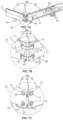
- FIGS. 1 A- 1 D illustrate an example of a manufacturing method applicable to manufacture of the circuit board assembly according to the invention.
- FIG. 1 A shows a circuit board 1 of a large size.
- FIG. 1 B is an enlarged view of a portion of an ellipse O indicated by a dotted line in FIG. 1 A .
- circuit board assemblies 100 are manufactured from the circuit board 1 of a large size.
- a portion to be a circuit board assembly 100 after manufacture is assigned the same reference numeral as that after the manufacture and is referred to as a circuit board assembly 100 even in a stage before being completed as the circuit board assembly 100 .
- FIGS. 1 A and 1 B a circuit pattern has already been printed, and punching has been further performed, to form respective prototypes of the first circuit board 10 and the second circuit board 20 .
- the first circuit board 10 and the second circuit board 20 respectively include a first circuit portion 11 and a second circuit portion 21 that are electrically connected to each other and function as an antenna.
- a third circuit portion 22 is further formed in the second circuit board 20 .
- the through holes 13 and 23 each correspond to an example of a receiving portion referred to herein.
- the receiving portion is not necessarily a through hole.
- FIG. 1 C is a diagram illustrating a state where the metal fitting 50 is inserted into the respective through holes 13 and 23 in the first circuit board 10 and the second circuit board 20 illustrated in FIGS. 1 A and 1 B .
- the metal fitting 50 is manufactured separately from the first circuit board 10 and the second circuit board 20 illustrated in FIGS. 1 B- 1 E .
- an example of the metal fitting 50 is a metal flat plate punched in a strip shape and bent to respectively insert both its end portions into the through holes 13 and 23 or a metal fitting including the metal flat plate.
- an element other than the metal flat plate such as a coating film such as an insulating coating film or a non-metallic structure for entirely increasing a strength may be further partially combined with the bent metal flat plate.
- the metal fitting 50 has its rigidity and electrical conductivity considered to take charge of mechanical coupling between the first circuit board 10 and the second circuit board 20 and also take charge of electrical connection therebetween.
- the metal fitting 50 has its both end portions respectively inserted into the through holes 13 and 23 , and is soldered thereto to pour solder into respective gaps between the through holes 13 and 23 and the end portions.
- FIG. 1 D is a diagram illustrating a state where the circuit board assembly 100 is separated from the frame 1 A of the circuit board 1 of a large size.
- the first circuit board 10 and the second circuit board 20 are coplanar.
- the circuit board assembly 100 is bent in a portion of the metal fitting 50 after being separated from the frame 1 A, as illustrated in FIG. 1 E .
- the circuit board assembly 100 is bent at an angle of 90° as an example.
- FIG. 1 E is an isometric view illustrating the circuit board assembly 100 and a third circuit board 30 after the bending.
- the third circuit board 30 corresponds to an example of a support portion referred to in the present embodiment.
- a first side 201 of the second circuit board 20 extends adjacent to and parallel to a first side 101 of the first circuit board 10 .
- the first circuit board 10 has a protrusion 14 protruding toward the third circuit board 30 from its second side 102 .
- the second circuit board 20 also has protrusions 24 and 25 protruding toward the third circuit board 30 from its second side 202 .
- Through holes 31 , 32 , and 33 are respectively formed at positions corresponding to the protrusions 14 , 24 , and 25 .
- the protrusions 14 , 24 , and 25 are respectively inserted into and soldered to the through holes 31 , 32 , and 33 .
- the protrusions 14 , 24 , and 25 and the through holes 31 , 32 , and 33 take charge of mechanical coupling and electrical connection between the first and second circuit boards 10 and 20 and the third circuit board 30 .
- respective partial circuits formed in the first circuit board 10 , the second circuit board 20 , and the third circuit board 30 are connected to one another to form one circuit.
- Each of the protrusions 14 , 24 , and 25 corresponds to an example of a protrusion referred to in the invention
- each of the through holes 31 , 32 and 33 corresponds to an example of an insertion portion referred to in the invention.
- the circuit board assembly 100 needs to be finished to a relative position and an opening angle between the first circuit board 10 and the second circuit board 20 , which have been strictly adjusted to such an extent that the protrusions 14 , 24 , and 25 can be respectively smoothly inserted into the through holes 31 , 32 , and 33 .
- the circuit board assembly 100 may be bent such that only a bending angle of the metal fitting 50 satisfies a defined accuracy.
- a circuit board assembly according to each of the embodiments described below can adopt the manufacturing method illustrated in FIGS. 1 A- 1 E so that time and cost required for manufacture can be reduced.
- the accuracy of a general through hole and a required assembly accuracy of two circuit boards are listed.
- FIGS. 2 A- 2 C illustrate the accuracy of a general through hole on a circuit board.
- FIG. 2 A illustrates the accuracy of a positional relationship between respective general through holes on circuit boards. The accuracy has a tolerance of ⁇ 0.1 mm to ⁇ 0.25 mm for a true relative distance X between two through holes.
- FIG. 2 B illustrates the accuracy of the diameter of a general through hole on a circuit board. The accuracy has a tolerance of ⁇ 0.05 mm to ⁇ 0.15 mm for a true diameter ⁇ x. The assembly accuracy of two circuit boards needs to be set in consideration of the accuracy of the diameter of the through hole.
- FIG. 2 C illustrates a gap in design between a general through hole on a circuit board and a terminal to be inserted into the through hole.
- the gap is set to 0.1 mm to 0.5 mm.
- a fixing force between the circuit boards with solder may be insufficient or unstable.
- FIGS. 3 A and 3 B illustrate a required accuracy of a relative position between terminals to be respectively smoothly inserted into through holes.
- the terminal corresponds to a protrusion 13 , 23 of each of the circuit boards 10 , 20 , and the protrusion 13 , 23 is a part of the circuit board 10 , 20 .
- the accuracy of the relative position between the terminals can be considered as the assembly accuracy of the two circuit boards 10 , 20 .
- a positional relationship between the protrusion 13 in the first circuit board 10 and the protrusion 23 in the second circuit board 20 is defined in two directions. As illustrated in FIG. 3 B , a distance between the center of the width of the protrusion 13 in the first circuit board 10 and the center of the thickness of the protrusion 23 in the second circuit board 20 is 15 mm, and a tolerance of the distance is ⁇ 0.25 mm. That is, it is defined that the distance is to be within a range from 14.75 mm to 15.25 mm.
- a distance between the center of the thickness of the protrusion 13 in the first circuit board 10 and the center of the width of the protrusion 23 in the second circuit board 23 is 5 mm, and a tolerance of the distance is ⁇ 0.25 mm. That is, it is specified that the distance is to be within a range from 4.75 mm to 5.25 mm.
- circuit board assemblies will be described by adopting reference numerals adopted in the circuit board assembly 100 illustrated in FIG. 1 as they are even if different in form for the sake of clarity. Overlapping description for a content described with reference to FIG. 1 and overlapping description for a content described in an embodiment listed above in embodiments listed below may be omitted.
- FIGS. 4 A- 4 C illustrate a circuit board assembly 100 according to a first embodiment of the invention.
- FIGS. 4 A, 4 B, and 4 C are respectively an isometric view of a circuit board assembly 100 , an enlarged view of a portion of a circle R indicated by a dotted line in FIG. 4 A , and an enlarged view illustrating the rear side of the portion of the circle R.
- the circuit board assembly 100 illustrated in FIG. 4 A is the same as the circuit board assembly 100 illustrated in FIG. 1 , and includes a first circuit board 10 , a second circuit board 20 , and a metal fitting 50 that connects the circuit boards.
- a first circuit portion 11 is formed in the first circuit board 10
- a second circuit portion 21 and a third circuit portion 22 are formed in the second circuit board 10 .
- the first circuit portion 11 and the second circuit portion 21 are electrically connected to each other by the metal fitting 50 , to constitute one antenna.
- the circuit board assembly 100 is adopted for the antenna, for example, an antenna having a stabler performance than that of a combination of the metal fitting and the electrical wiring is implemented.
- Through holes 13 and 23 are respectively formed in the first circuit board 10 and the second circuit board 20 , and end portions 51 and 52 of the metal fitting 50 are respectively inserted into the through holes 13 and 23 .
- both the end portions 51 and 52 are respectively inserted into the through holes 13 and 23 , and solder is poured into and attached to respective gaps between the through holes 13 and 23 and the end portions 51 and 52 of the metal fitting 50 inserted into the through holes 13 and 23 .
- the metal fitting 50 mechanically connects the first circuit board 10 and the second circuit board 20 to each other.
- the metal fitting 50 illustrated on the upper side also electrically connects the first circuit portion 11 and the second circuit portion 21 to each other.
- a protrusion 14 is formed in the first circuit board 10
- protrusions 24 and 25 are formed in the second circuit board 20 .
- the metal fitting 50 is a metal flat plate punched in a strip shape and bent to respectively insert both its end portions into the through holes 13 and 23 .
- both the end portions 51 and 52 are respectively inserted into and soldered to the through holes 13 and 23 , and a central portion 53 is further bent at a predetermined angle (90° herein).
- first circuit board 10 and the second circuit board 20 are connected to each other by a jumper wire instead of the metal fitting 50 .
- the jumper wire is for electrical connection, and a soft material having a relatively low rigidity is used for convenient handling. Accordingly, even if the first circuit board 10 and the second circuit board 20 are connected to each other by the jumper wire and the jumper wire is bent once such that a predetermined angle is formed between the first circuit board 10 and the second circuit board 20 , a relative posture between the first circuit board 10 and the second circuit board 20 may change due to an action of gravity in the middle of handling.
- metal fitting 50 to be adopted is a metal fitting 50 made of a material, dimensions, and the like rigid enough to maintain a predetermined tolerance for an angle between the first circuit board 10 and the second circuit board 20 even if a posture in a direction of gravity of the circuit board assembly 100 is changed if bent once.
- FIGS. 5 A- 5 C illustrates a circuit board assembly 100 according to a second embodiment of the invention.
- FIGS. 5 A, 5 B, and 5 C are respectively an isometric view of a circuit board assembly 100 , an enlarged view of a portion of a circle R indicated by a dotted line in FIG. 5 A , and an enlarged view illustrating the rear side of the portion of the circle R.
- a difference of the second embodiment illustrated in FIG. 5 from the first embodiment illustrated in FIG. 4 is a shape of both end portions 51 and 52 of a metal fitting 50 .
- Both the end portions 51 and 52 of the metal fitting 50 are respectively provided with holes 511 and 521 , and the end portions 51 and 52 are respectively inserted into through holes 13 and 23 to crush the holes 511 and 521 . That is, the end portions 51 and 52 are respectively press-fitted into the through holes 13 and 23 .
- the metal fitting 50 may connect the first circuit board 10 and the second circuit board 20 to each other by the press fitting.
- the metal fitting 50 is also obtained by punching a metal flat plate in a strip shape and bending both its end portions 51 and 52 and further bending its central portion 53 , and corresponds to an example of a bent plate-shaped metal fitting referred to in the invention.
- the first circuit board 10 and the second circuit board 20 may be more firmly connected to each other by both press-fitting and soldering, although connected to each other by only press-fitting of both the end portions 51 and 52 of the metal fitting 50 in the second embodiment.
- FIGS. 6 A- 6 C illustrate a circuit board assembly 100 according to a third embodiment of the invention.
- FIGS. 6 A, 6 B, and 6 C are respectively an isometric view of a circuit board assembly 100 , an enlarged view of a portion of a circle R indicated by a dotted line in FIG. 6 A , and an enlarged view illustrating the rear side of the portion of the circle R.
- a difference of the third embodiment illustrated in FIGS. 6 A- 6 C from the first embodiment illustrated in FIGS. 4 A- 4 C is relative dimensions of both end portions 51 and 52 of a metal fitting 50 and through holes 13 and 23 and the width of a central portion 53 of the metal fitting 50 .
- a width w of the metal fitting 50 is smaller than the diameter of the through holes 13 and 23 , and both the end portions 51 and 52 are fixed to each other by soldering after being respectively inserted into the through holes 13 and 23 .
- a width w of the metal fitting 50 is made slightly larger than the diameter of the through holes 13 and 23 , and both the end portions 51 and 52 are respectively press-fitted into the through holes 13 and 23 , although a cross sectional shape of both the end portions 51 and 52 of the metal fitting 50 remains rectangular, like in the first embodiment.
- the end portions 51 and 52 may be more firmly fixed to each other using press fitting and soldering in combination.
- a width w 2 of the central portion 53 is smaller than a width w 1 of both the end portions 51 and 52 . This is because a position where the metal fitting 50 is bent is guided to the central portion 53 to make it easy to bend the central portion 53 at a correct angle when an angle is formed between the first circuit board 10 and the second circuit board 20 .
- the metal fitting 50 illustrated in FIGS. 6 A- 6 C is also obtained by punching a metal flat plate in a strip shape and bending both its end portions 51 and 52 and further bending its central portion 53 , and corresponds to an example of a bent plate-shaped metal fitting referred to in the invention.
- Both the end portions 51 and 52 of the metal fitting 50 may be respectively inserted into and soldered to the through holes 13 and 23 , or may be respectively press-fitted into the through holes 13 and 23 , or soldering and press fitting may be used in combination, as illustrated in the examples described above. This point is similar to that in each of embodiments described below, and reference to a method for respectively fixing both end portions 51 and 52 of a metal fitting 50 into through holes 13 and 23 is omitted.
- FIGS. 7 A- 7 C illustrate a circuit board assembly 100 according to a fourth embodiment of the invention.
- FIGS. 7 A, 7 B, and 7 C are respectively an isometric view of a circuit board assembly 100 , an enlarged view of a portion of a circle R indicated by a dotted line in FIG. 7 A , and an enlarged view illustrating the rear side of the portion of the circle R.
- the wall thickness of a central portion 53 is smaller than that of both end portions 51 and 52 . This is also for making it easy to bend the central portion 53 , like in the third embodiment illustrated in FIG. 6 .
- the metal fitting 50 illustrated in FIGS. 7 A- 7 C is also obtained by punching a metal flat plate in a strip shape, crushing its central portion 53 such that the wall thickness thereof decreases at the time of the punching, and bending both its end portions 51 and 52 and further bending the central portion 53 , and corresponds to an example of a bent plate-shaped metal fitting referred to in the invention.
- FIGS. 8 A- 8 C illustrate a circuit board assembly according to a fifth embodiment of the invention.
- FIGS. 8 A, 8 B, and 8 C are respectively an isometric view of a circuit board assembly 100 , an enlarged view of a portion of a circle R indicated by a dotted line in FIG. 8 A , and an enlarged view illustrating the rear side of the portion of the circle R.
- a metal fitting 50 in the fifth embodiment illustrated in FIGS. 8 A- 8 C a width w 2 of a central portion 53 is smaller than a width w 1 of both end portions 51 and 52 .
- the metal fitting 50 increases in width toward both the end portions 51 and 52 . This is for making it easy to bend the central portion 53 .
- the metal fitting 50 illustrated in FIGS. 8 A- 8 C is also obtained by punching a metal flat plate in a strip shape and bending both its end portions 51 and 52 and further bending its central portion 53 , and corresponds to an example of a bent plate-shaped metal fitting referred to in the invention.
- FIGS. 9 A- 9 C is a diagram illustrating a circuit board assembly 100 according to a sixth embodiment of the invention.
- FIGS. 9 A, 9 B, and 9 C are respectively an isometric view of a circuit board assembly 100 , an enlarged view of a portion of a circle R indicated by a dotted line in FIG. 9 A , and an enlarged view illustrating the rear side of the portion of the circle R.
- each of both end portions 51 and 52 is two-pronged.
- two through holes 13 in a first circuit board 10 and two through holes 23 in a second circuit board 20 are also formed for each metal fitting 50 .
- Both the two-pronged end portions 51 and the two-pronged end portions 52 are respectively inserted into the two through holes 13 and the two through holes 23 .
- the metal fitting 50 illustrated in FIGS. 9 A- 9 C is also obtained by punching a metal flat plate and bending both its end portions 51 and 52 and further bending its central portion 53 , and corresponds to an example of a bent plate-shaped metal fitting referred to in the invention.
- FIGS. 10 A- 10 C illustrate a circuit board assembly according to a seventh embodiment of the invention.
- FIGS. 10 A, 10 B, and 10 C are respectively an isometric view of a circuit board assembly 100 , an enlarged view of a portion of a circle R indicated by a dotted line in FIG. 10 A , and an enlarged view illustrating the rear side of the portion of the circle R.
- each of both end portions 51 and 52 is three-pronged.
- three through holes 13 in a first circuit board 10 and three through holes 23 in a second circuit board 20 are also formed for each metal fitting 50 .
- Both the three-pronged end portions 51 and the three-pronged end portions 52 are respectively inserted into the three through holes 13 and the three through holes 23 .
- the reason why each of both the end portions 51 and 52 is three-pronged is the same as the reason why each of both the end portions 51 is two-pronged.
- the metal fitting 50 illustrated in FIGS. 10 A- 10 C is also obtained by punching a metal flat plate and bending both its end portions 51 and 52 and further bending its central portion 53 , and corresponds to an example of a bent plate-shaped metal fitting referred to in the invention.
- FIGS. 11 A- 11 C is a diagram illustrating a circuit board assembly 100 according to an eighth embodiment of the invention.
- FIGS. 11 A, 11 B, and 11 C are respectively an isometric view of a circuit board assembly 100 , an enlarged view of a portion of a circle R indicated by a dotted line in FIG. 11 A , and an enlarged view illustrating the rear side of the portion of the circle R.
- the metal fitting 50 couples the first circuit board 10 and the second circuit board 20 to each other via the side at an obtuse angle (the side opened at an angle of 270°).
- the circuit board assembly 100 in the eighth embodiment illustrated in FIGS. 11 A- 11 C couples a first circuit board 10 and a second circuit board 20 to each other via the side at an acute angle (the side opened at an angle of 90°).
- a metal fitting 50 illustrated in FIGS. 11 A- 11 C is also obtained by punching a metal flat plate and bending both its end portions 51 and 52 and further bending its central portion 53 , and corresponds to an example of a bent plate-shaped metal fitting referred to in the invention.
- FIGS. 12 A- 12 C illustrate a circuit board assembly 100 according to a ninth embodiment of the invention.
- FIGS. 12 A, 12 B, and 12 C are respectively an isometric view of a circuit board assembly 100 , an enlarged view of a portion of a circle R indicated by a dotted line in FIG. 12 A , and an enlarged view illustrating the rear side of the portion of the circle R.
- the through holes 13 and 23 are respectively formed in the first circuit board 10 and the second circuit board 20 , and the metal fitting 50 couples the first circuit board 10 and the second circuit board 20 to each other with both the end portions 51 and 52 respectively inserted into the through holes 13 and 23 .
- the circuit board assembly 100 according to the ninth embodiment illustrated in FIGS. 12 A- 12 C are bent in a direction in which both end portions 51 and 52 of a metal fitting 50 are respectively bent in a direction along respective surfaces of a first circuit board 10 and a second circuit board 20 , and are respectively soldered to the surfaces of the first circuit board 10 and the second circuit board 20 .
- the metal fitting 50 may be soldered to the respective surfaces of the first circuit board 10 and the second circuit board 20 .
- the metal fitting 50 illustrated in FIGS. 12 A- 12 C is also obtained by punching a metal flat plate and bending both its end portions 51 and 52 and further bending its central portion 53 , and corresponds to an example of a bent plate-shaped metal fitting referred to in the invention.
- FIGS. 13 A- 13 C illustrate a circuit board assembly according to a tenth embodiment of the invention.
- FIGS. 13 A, 13 B, and 13 C are respectively an isometric view of a circuit board assembly 100 , an enlarged view of a portion of a circle R indicated by a dotted line in FIG. 13 A , and an enlarged view illustrating the rear side of the portion of the circle R.
- the first circuit board 10 and the second circuit board 20 are coupled to each other by the two metal fittings 50 .
- a first circuit board 10 and a second circuit board 20 are connected to each other by one metal fitting 50 having a large width w.
- the number of metal fittings 50 is one, two through holes 13 and two through holes 23 are respectively formed in the first circuit board 10 and the second circuit board 20 .
- two leg portions 512 and two leg portions 522 are respectively formed in both end portions 51 and 52 of the metal fitting 50 , and the one leg portion 512 and the one leg portion 522 are respectively inserted into each of the through holes 13 and each of the through holes 23 .
- a hole 531 is formed in a central portion 53 of the metal fitting 50 such that the central portion 53 can be bent with an appropriate force.
- the number of metal fittings 50 that each couple the first circuit board 10 and the second circuit board 20 to each other need not be two, may be one, as illustrated in FIGS. 13 A- 13 C , or may be three or more, although illustration thereof is omitted.
- the metal fitting 50 illustrated in FIGS. 13 A- 13 C is also obtained by punching a metal flat plate and bending both its end portions 51 and 52 and further bending its central portion 53 , and corresponds to an example of a bent plate-shaped metal fitting referred to in the invention.
- FIGS. 14 A- 14 C illustrate a circuit board assembly 100 according to an eleventh embodiment of the invention.
- FIGS. 14 A, 14 B, and 14 C are respectively an isometric view of a circuit board assembly 100 as viewed from the front surface side thereof and an isometric view and a side view of the circuit board assembly 100 as viewed from the rear surface side thereof.
- the metal fitting 50 couples the first circuit board 10 and the second circuit board 20 to each other to maintain a posture in which the first circuit board 10 and the second circuit board 20 are opened at an angle of 90°.
- the circuit board assembly 100 according to the eleventh embodiment illustrated in FIGS. 14 A- 14 C couples a first circuit board 10 and a second circuit board 20 to each other to maintain a posture in which the first circuit board 10 and the second circuit board 20 are opened at an angle of not 90° but 120°, for example.
- An angle formed between the first circuit board 10 and the second circuit board 20 need not be 90° but may be any angle excluding 180°, as illustrated in FIGS. 14 A- 14 C .
- a metal fitting 50 illustrated in FIGS. 14 A- 14 C is also obtained by punching a metal flat plate and bending both its end portions 51 and 52 and further bending its central portion 53 , and corresponds to an example of a bent plate-shaped metal fitting referred to in the invention.
- FIGS. 15 A and 15 B illustrate a circuit board assembly 100 according to a twelfth embodiment of the invention.
- FIGS. 15 A and 15 B are respectively isometric views of a circuit board assembly 100 as viewed from the front surface side and the rear surface side thereof.
- the circuit board assembly 100 has a structure in which the two circuit boards, i.e., the first circuit board 10 and the second circuit board 20 are connected to each other by the metal fitting 50 .
- the circuit board assembly 100 illustrated in FIGS. 15 A and 15 B further includes a fourth circuit board 40 and a metal fitting 60 .
- the fourth circuit board 40 is connected to a first circuit board 10 by the metal fitting 60 .
- the circuit board assembly 100 may have a structure obtained by connecting three or more circuit boards to one another.
- the metal fitting 60 shown in FIGS. 15 A and 15 B is also obtained by punching a metal flat plate and bending both its end portions and further bending its central portion, and corresponds to an example of a bent plate-shaped metal fitting referred to in the invention.
- an angle between circuit boards and a positional relationship between the circuit boards are strictly adjusted, and a circuit board assembly that has attained low cost is implemented, as illustrated in the first to twelfth embodiments.
Landscapes
- Engineering & Computer Science (AREA)
- Microelectronics & Electronic Packaging (AREA)
- Manufacturing & Machinery (AREA)
- Combinations Of Printed Boards (AREA)
- Coupling Device And Connection With Printed Circuit (AREA)
Abstract
Description
Claims (15)
Applications Claiming Priority (2)
| Application Number | Priority Date | Filing Date | Title |
|---|---|---|---|
| JP2021-084915 | 2021-05-19 | ||
| JP2021084915A JP7770785B2 (en) | 2021-05-19 | 2021-05-19 | Method for manufacturing a circuit board assembly |
Publications (2)
| Publication Number | Publication Date |
|---|---|
| US20220377891A1 US20220377891A1 (en) | 2022-11-24 |
| US12225664B2 true US12225664B2 (en) | 2025-02-11 |
Family
ID=81850568
Family Applications (1)
| Application Number | Title | Priority Date | Filing Date |
|---|---|---|---|
| US17/747,349 Active 2043-03-18 US12225664B2 (en) | 2021-05-19 | 2022-05-18 | Circuit board assembly |
Country Status (5)
| Country | Link |
|---|---|
| US (1) | US12225664B2 (en) |
| EP (1) | EP4093161A1 (en) |
| JP (1) | JP7770785B2 (en) |
| KR (1) | KR20220156766A (en) |
| CN (1) | CN115379641A (en) |
Citations (12)
| Publication number | Priority date | Publication date | Assignee | Title |
|---|---|---|---|---|
| US6075708A (en) | 1997-09-04 | 2000-06-13 | Rohm Co., Ltd. | Partly bent electric circuit substrate and method for manufacturing the same |
| EP1091626A1 (en) | 1998-05-28 | 2001-04-11 | Rohm Co., Ltd. | Circuit board of protective circuit for storage battery, protective circuit for storage battery, and storage battery pack |
| US6520789B2 (en) * | 2001-05-22 | 2003-02-18 | Delphi Technologies, Inc. | Connecting system for printed circuit boards |
| JP2004311813A (en) | 2003-04-09 | 2004-11-04 | Matsushita Electric Ind Co Ltd | Substrate equipment |
| US20060067066A1 (en) * | 2004-09-27 | 2006-03-30 | Meier Pascal C | Flexible cable for high-speed interconnect |
| DE102007046493A1 (en) | 2007-09-28 | 2009-04-09 | Continental Automotive Gmbh | Three-dimensional electronic circuit carrier structure, as well as circuit base carrier having the circuit carrier structure as a functional component and three-dimensional circuit arrangement consisting of at least two such three-dimensional circuit carrier structures |
| US20110122045A1 (en) * | 2009-11-23 | 2011-05-26 | Samsung Electronics Co. Ltd. | Built-in printed circuit board antenna of mobile terminal |
| US20160192515A1 (en) * | 2014-12-25 | 2016-06-30 | Delta Electronics, Inc. | Circuit board assembly and assembling method thereof |
| JP2019134081A (en) | 2018-01-31 | 2019-08-08 | 株式会社デンソー | Electronic circuit |
| JP2020025012A (en) | 2018-08-07 | 2020-02-13 | タイコエレクトロニクスジャパン合同会社 | Terminal-equipped circuit board and circuit board assembly |
| EP3697182A1 (en) | 2018-08-28 | 2020-08-19 | Lg Chem, Ltd. | Printed circuit board assembly and method for manufacturing same |
| US20220225525A1 (en) * | 2019-06-06 | 2022-07-14 | Omron Corporation | Electronic device |
Family Cites Families (4)
| Publication number | Priority date | Publication date | Assignee | Title |
|---|---|---|---|---|
| JPS575386A (en) * | 1980-06-11 | 1982-01-12 | Matsushita Electric Industrial Co Ltd | Printed circuit board device |
| JPH08236895A (en) * | 1995-02-24 | 1996-09-13 | Toshiba Mec Kk | Printed wiring board |
| JP3713682B2 (en) * | 2001-12-21 | 2005-11-09 | 日本航空電子工業株式会社 | Board mounting structure |
| WO2018164206A1 (en) * | 2017-03-07 | 2018-09-13 | Ngkエレクトロデバイス株式会社 | Insulation circuit board terminal, insulation circuit board composite body, and semiconductor device composite body |
-
2021
- 2021-05-19 JP JP2021084915A patent/JP7770785B2/en active Active
-
2022
- 2022-05-16 CN CN202210528434.3A patent/CN115379641A/en active Pending
- 2022-05-18 US US17/747,349 patent/US12225664B2/en active Active
- 2022-05-18 KR KR1020220060913A patent/KR20220156766A/en active Pending
- 2022-05-18 EP EP22174198.6A patent/EP4093161A1/en active Pending
Patent Citations (15)
| Publication number | Priority date | Publication date | Assignee | Title |
|---|---|---|---|---|
| US6075708A (en) | 1997-09-04 | 2000-06-13 | Rohm Co., Ltd. | Partly bent electric circuit substrate and method for manufacturing the same |
| EP1091626A1 (en) | 1998-05-28 | 2001-04-11 | Rohm Co., Ltd. | Circuit board of protective circuit for storage battery, protective circuit for storage battery, and storage battery pack |
| US6520789B2 (en) * | 2001-05-22 | 2003-02-18 | Delphi Technologies, Inc. | Connecting system for printed circuit boards |
| JP2004311813A (en) | 2003-04-09 | 2004-11-04 | Matsushita Electric Ind Co Ltd | Substrate equipment |
| US20060067066A1 (en) * | 2004-09-27 | 2006-03-30 | Meier Pascal C | Flexible cable for high-speed interconnect |
| DE102007046493A1 (en) | 2007-09-28 | 2009-04-09 | Continental Automotive Gmbh | Three-dimensional electronic circuit carrier structure, as well as circuit base carrier having the circuit carrier structure as a functional component and three-dimensional circuit arrangement consisting of at least two such three-dimensional circuit carrier structures |
| US20110122045A1 (en) * | 2009-11-23 | 2011-05-26 | Samsung Electronics Co. Ltd. | Built-in printed circuit board antenna of mobile terminal |
| US20160192515A1 (en) * | 2014-12-25 | 2016-06-30 | Delta Electronics, Inc. | Circuit board assembly and assembling method thereof |
| JP2019134081A (en) | 2018-01-31 | 2019-08-08 | 株式会社デンソー | Electronic circuit |
| US20200359498A1 (en) | 2018-01-31 | 2020-11-12 | Denso Corporation | Electronic circuit |
| US11191161B2 (en) | 2018-01-31 | 2021-11-30 | Denso Corporation | Electronic circuit |
| JP2020025012A (en) | 2018-08-07 | 2020-02-13 | タイコエレクトロニクスジャパン合同会社 | Terminal-equipped circuit board and circuit board assembly |
| US20210159623A1 (en) | 2018-08-07 | 2021-05-27 | Tyco Electronics Japan G.K. | Circuit Board Having Terminal, And Circuit Board Assembly |
| EP3697182A1 (en) | 2018-08-28 | 2020-08-19 | Lg Chem, Ltd. | Printed circuit board assembly and method for manufacturing same |
| US20220225525A1 (en) * | 2019-06-06 | 2022-07-14 | Omron Corporation | Electronic device |
Non-Patent Citations (1)
| Title |
|---|
| Extended Search Report from the European Patent Office dated Sep. 28, 2022, corresponding to Application No. 22174198.6-1202, 8 pages. |
Also Published As
| Publication number | Publication date |
|---|---|
| US20220377891A1 (en) | 2022-11-24 |
| JP7770785B2 (en) | 2025-11-17 |
| JP2022178257A (en) | 2022-12-02 |
| EP4093161A1 (en) | 2022-11-23 |
| CN115379641A (en) | 2022-11-22 |
| KR20220156766A (en) | 2022-11-28 |
Similar Documents
| Publication | Publication Date | Title |
|---|---|---|
| US4923414A (en) | Compliant section for circuit board contact elements | |
| US7086913B2 (en) | Surface mount header assembly having a planar alignment surface | |
| JPH0869828A (en) | Press-in terminal of connector and its manufacture | |
| JP2001006771A (en) | Connector | |
| KR20140072913A (en) | Tuning fork electrical contact with prongs having non-rectangular shape | |
| CN106663886A (en) | Terminal-equipped printed circuit board | |
| US7210969B1 (en) | Press-fit fixing terminal, and electronic component having the same terminal | |
| JP2005353567A (en) | Press-fit terminal and circuit board module using the same | |
| US6442036B2 (en) | Substrate mount type terminal | |
| CN114256651A (en) | Connector with a locking member | |
| JP2005294217A (en) | Pressure contact type contact and electrical connector using the same | |
| KR20170055008A (en) | Terminal, circuit-board comprising the termianl | |
| CN113196576A (en) | Wire harness member | |
| US12225664B2 (en) | Circuit board assembly | |
| EP3522305A1 (en) | On-board diagnostic system connector terminal and on-board diagnostic system | |
| US20250055212A1 (en) | Dual entry card edge connector | |
| US7044812B2 (en) | Surface mount header assembly having a planar alignment surface | |
| CN110233373B (en) | Connector component | |
| JP3340697B2 (en) | Method of manufacturing connector and its housing | |
| JPH0245305B2 (en) | ||
| JP2017216079A (en) | Board terminal | |
| EP3940891B1 (en) | Contact | |
| JP2021114397A (en) | connector | |
| KR100215575B1 (en) | Connector for electric / electronic device | |
| US20220059961A1 (en) | Connector with built-in substrate and method of manufacturing chain terminal of the connector with built-in substrate |
Legal Events
| Date | Code | Title | Description |
|---|---|---|---|
| FEPP | Fee payment procedure |
Free format text: ENTITY STATUS SET TO UNDISCOUNTED (ORIGINAL EVENT CODE: BIG.); ENTITY STATUS OF PATENT OWNER: LARGE ENTITY |
|
| STPP | Information on status: patent application and granting procedure in general |
Free format text: DOCKETED NEW CASE - READY FOR EXAMINATION |
|
| AS | Assignment |
Owner name: TYCO ELECTRONICS JAPAN G.K., JAPAN Free format text: ASSIGNMENT OF ASSIGNORS INTEREST;ASSIGNORS:DOBASHI, DAISUKE;KIMURA, TAKESHI;SIGNING DATES FROM 20221014 TO 20221017;REEL/FRAME:061768/0411 |
|
| STPP | Information on status: patent application and granting procedure in general |
Free format text: NON FINAL ACTION MAILED |
|
| STPP | Information on status: patent application and granting procedure in general |
Free format text: RESPONSE TO NON-FINAL OFFICE ACTION ENTERED AND FORWARDED TO EXAMINER |
|
| STPP | Information on status: patent application and granting procedure in general |
Free format text: FINAL REJECTION MAILED |
|
| STPP | Information on status: patent application and granting procedure in general |
Free format text: RESPONSE AFTER FINAL ACTION FORWARDED TO EXAMINER |
|
| STPP | Information on status: patent application and granting procedure in general |
Free format text: NOTICE OF ALLOWANCE MAILED -- APPLICATION RECEIVED IN OFFICE OF PUBLICATIONS |
|
| AS | Assignment |
Owner name: TE CONNECTIVITY JAPAN G.K., JAPAN Free format text: CHANGE OF NAME;ASSIGNOR:TYCO ELECTRONICS JAPAN G.K.;REEL/FRAME:069811/0353 Effective date: 20241001 |
|
| STPP | Information on status: patent application and granting procedure in general |
Free format text: PUBLICATIONS -- ISSUE FEE PAYMENT VERIFIED |
|
| STCF | Information on status: patent grant |
Free format text: PATENTED CASE |