US12223914B2 - Display device and method of driving the same - Google Patents
Display device and method of driving the same Download PDFInfo
- Publication number
- US12223914B2 US12223914B2 US18/206,409 US202318206409A US12223914B2 US 12223914 B2 US12223914 B2 US 12223914B2 US 202318206409 A US202318206409 A US 202318206409A US 12223914 B2 US12223914 B2 US 12223914B2
- Authority
- US
- United States
- Prior art keywords
- initialization
- scan
- scan signal
- supplied
- signal
- Prior art date
- Legal status (The legal status is an assumption and is not a legal conclusion. Google has not performed a legal analysis and makes no representation as to the accuracy of the status listed.)
- Active
Links
- 238000000034 method Methods 0.000 title claims description 24
- 239000003990 capacitor Substances 0.000 claims description 21
- 230000003247 decreasing effect Effects 0.000 claims description 12
- 238000010586 diagram Methods 0.000 description 55
- 235000019557 luminance Nutrition 0.000 description 55
- 230000004044 response Effects 0.000 description 19
- 102100040862 Dual specificity protein kinase CLK1 Human genes 0.000 description 9
- 102100040858 Dual specificity protein kinase CLK4 Human genes 0.000 description 9
- 101000749294 Homo sapiens Dual specificity protein kinase CLK1 Proteins 0.000 description 9
- 101000749298 Homo sapiens Dual specificity protein kinase CLK4 Proteins 0.000 description 9
- 102100040844 Dual specificity protein kinase CLK2 Human genes 0.000 description 6
- 102100040856 Dual specificity protein kinase CLK3 Human genes 0.000 description 6
- 101000749291 Homo sapiens Dual specificity protein kinase CLK2 Proteins 0.000 description 6
- 101000749304 Homo sapiens Dual specificity protein kinase CLK3 Proteins 0.000 description 6
- 101150080315 SCS2 gene Proteins 0.000 description 5
- 101100072644 Saccharomyces cerevisiae (strain ATCC 204508 / S288c) INO2 gene Proteins 0.000 description 5
- 101100454372 Saccharomyces cerevisiae (strain ATCC 204508 / S288c) LCB2 gene Proteins 0.000 description 5
- 101100029960 Saccharomyces cerevisiae (strain ATCC 204508 / S288c) PLM2 gene Proteins 0.000 description 5
- 101100489624 Saccharomyces cerevisiae (strain ATCC 204508 / S288c) RTS1 gene Proteins 0.000 description 5
- 101100256290 Saccharomyces cerevisiae (strain ATCC 204508 / S288c) SCS3 gene Proteins 0.000 description 5
- 101100256289 Schizosaccharomyces pombe (strain 972 / ATCC 24843) fit1 gene Proteins 0.000 description 5
- 230000014509 gene expression Effects 0.000 description 5
- 230000008859 change Effects 0.000 description 4
- 241001270131 Agaricus moelleri Species 0.000 description 3
- 238000005259 measurement Methods 0.000 description 3
- 230000000694 effects Effects 0.000 description 2
- 230000008569 process Effects 0.000 description 2
- 238000005070 sampling Methods 0.000 description 2
- 230000008878 coupling Effects 0.000 description 1
- 238000010168 coupling process Methods 0.000 description 1
- 238000005859 coupling reaction Methods 0.000 description 1
- 238000005516 engineering process Methods 0.000 description 1
- 239000011147 inorganic material Substances 0.000 description 1
- 229910010272 inorganic material Inorganic materials 0.000 description 1
- 239000004973 liquid crystal related substance Substances 0.000 description 1
- 239000011368 organic material Substances 0.000 description 1
- 239000002096 quantum dot Substances 0.000 description 1
- 230000003252 repetitive effect Effects 0.000 description 1
Images


Classifications
-
- G—PHYSICS
- G09—EDUCATION; CRYPTOGRAPHY; DISPLAY; ADVERTISING; SEALS
- G09G—ARRANGEMENTS OR CIRCUITS FOR CONTROL OF INDICATING DEVICES USING STATIC MEANS TO PRESENT VARIABLE INFORMATION
- G09G3/00—Control arrangements or circuits, of interest only in connection with visual indicators other than cathode-ray tubes
- G09G3/20—Control arrangements or circuits, of interest only in connection with visual indicators other than cathode-ray tubes for presentation of an assembly of a number of characters, e.g. a page, by composing the assembly by combination of individual elements arranged in a matrix no fixed position being assigned to or needed to be assigned to the individual characters or partial characters
- G09G3/22—Control arrangements or circuits, of interest only in connection with visual indicators other than cathode-ray tubes for presentation of an assembly of a number of characters, e.g. a page, by composing the assembly by combination of individual elements arranged in a matrix no fixed position being assigned to or needed to be assigned to the individual characters or partial characters using controlled light sources
- G09G3/30—Control arrangements or circuits, of interest only in connection with visual indicators other than cathode-ray tubes for presentation of an assembly of a number of characters, e.g. a page, by composing the assembly by combination of individual elements arranged in a matrix no fixed position being assigned to or needed to be assigned to the individual characters or partial characters using controlled light sources using electroluminescent panels
- G09G3/32—Control arrangements or circuits, of interest only in connection with visual indicators other than cathode-ray tubes for presentation of an assembly of a number of characters, e.g. a page, by composing the assembly by combination of individual elements arranged in a matrix no fixed position being assigned to or needed to be assigned to the individual characters or partial characters using controlled light sources using electroluminescent panels semiconductive, e.g. using light-emitting diodes [LED]
- G09G3/3208—Control arrangements or circuits, of interest only in connection with visual indicators other than cathode-ray tubes for presentation of an assembly of a number of characters, e.g. a page, by composing the assembly by combination of individual elements arranged in a matrix no fixed position being assigned to or needed to be assigned to the individual characters or partial characters using controlled light sources using electroluminescent panels semiconductive, e.g. using light-emitting diodes [LED] organic, e.g. using organic light-emitting diodes [OLED]
- G09G3/3225—Control arrangements or circuits, of interest only in connection with visual indicators other than cathode-ray tubes for presentation of an assembly of a number of characters, e.g. a page, by composing the assembly by combination of individual elements arranged in a matrix no fixed position being assigned to or needed to be assigned to the individual characters or partial characters using controlled light sources using electroluminescent panels semiconductive, e.g. using light-emitting diodes [LED] organic, e.g. using organic light-emitting diodes [OLED] using an active matrix
- G09G3/3233—Control arrangements or circuits, of interest only in connection with visual indicators other than cathode-ray tubes for presentation of an assembly of a number of characters, e.g. a page, by composing the assembly by combination of individual elements arranged in a matrix no fixed position being assigned to or needed to be assigned to the individual characters or partial characters using controlled light sources using electroluminescent panels semiconductive, e.g. using light-emitting diodes [LED] organic, e.g. using organic light-emitting diodes [OLED] using an active matrix with pixel circuitry controlling the current through the light-emitting element
-
- G—PHYSICS
- G09—EDUCATION; CRYPTOGRAPHY; DISPLAY; ADVERTISING; SEALS
- G09G—ARRANGEMENTS OR CIRCUITS FOR CONTROL OF INDICATING DEVICES USING STATIC MEANS TO PRESENT VARIABLE INFORMATION
- G09G3/00—Control arrangements or circuits, of interest only in connection with visual indicators other than cathode-ray tubes
- G09G3/20—Control arrangements or circuits, of interest only in connection with visual indicators other than cathode-ray tubes for presentation of an assembly of a number of characters, e.g. a page, by composing the assembly by combination of individual elements arranged in a matrix no fixed position being assigned to or needed to be assigned to the individual characters or partial characters
- G09G3/22—Control arrangements or circuits, of interest only in connection with visual indicators other than cathode-ray tubes for presentation of an assembly of a number of characters, e.g. a page, by composing the assembly by combination of individual elements arranged in a matrix no fixed position being assigned to or needed to be assigned to the individual characters or partial characters using controlled light sources
- G09G3/30—Control arrangements or circuits, of interest only in connection with visual indicators other than cathode-ray tubes for presentation of an assembly of a number of characters, e.g. a page, by composing the assembly by combination of individual elements arranged in a matrix no fixed position being assigned to or needed to be assigned to the individual characters or partial characters using controlled light sources using electroluminescent panels
- G09G3/32—Control arrangements or circuits, of interest only in connection with visual indicators other than cathode-ray tubes for presentation of an assembly of a number of characters, e.g. a page, by composing the assembly by combination of individual elements arranged in a matrix no fixed position being assigned to or needed to be assigned to the individual characters or partial characters using controlled light sources using electroluminescent panels semiconductive, e.g. using light-emitting diodes [LED]
- G09G3/3208—Control arrangements or circuits, of interest only in connection with visual indicators other than cathode-ray tubes for presentation of an assembly of a number of characters, e.g. a page, by composing the assembly by combination of individual elements arranged in a matrix no fixed position being assigned to or needed to be assigned to the individual characters or partial characters using controlled light sources using electroluminescent panels semiconductive, e.g. using light-emitting diodes [LED] organic, e.g. using organic light-emitting diodes [OLED]
- G09G3/3266—Details of drivers for scan electrodes
-
- H—ELECTRICITY
- H10—SEMICONDUCTOR DEVICES; ELECTRIC SOLID-STATE DEVICES NOT OTHERWISE PROVIDED FOR
- H10K—ORGANIC ELECTRIC SOLID-STATE DEVICES
- H10K59/00—Integrated devices, or assemblies of multiple devices, comprising at least one organic light-emitting element covered by group H10K50/00
- H10K59/10—OLED displays
- H10K59/12—Active-matrix OLED [AMOLED] displays
- H10K59/121—Active-matrix OLED [AMOLED] displays characterised by the geometry or disposition of pixel elements
-
- H—ELECTRICITY
- H10—SEMICONDUCTOR DEVICES; ELECTRIC SOLID-STATE DEVICES NOT OTHERWISE PROVIDED FOR
- H10K—ORGANIC ELECTRIC SOLID-STATE DEVICES
- H10K59/00—Integrated devices, or assemblies of multiple devices, comprising at least one organic light-emitting element covered by group H10K50/00
- H10K59/10—OLED displays
- H10K59/12—Active-matrix OLED [AMOLED] displays
- H10K59/123—Connection of the pixel electrodes to the thin film transistors [TFT]
-
- G—PHYSICS
- G09—EDUCATION; CRYPTOGRAPHY; DISPLAY; ADVERTISING; SEALS
- G09G—ARRANGEMENTS OR CIRCUITS FOR CONTROL OF INDICATING DEVICES USING STATIC MEANS TO PRESENT VARIABLE INFORMATION
- G09G2300/00—Aspects of the constitution of display devices
- G09G2300/04—Structural and physical details of display devices
- G09G2300/0439—Pixel structures
-
- G—PHYSICS
- G09—EDUCATION; CRYPTOGRAPHY; DISPLAY; ADVERTISING; SEALS
- G09G—ARRANGEMENTS OR CIRCUITS FOR CONTROL OF INDICATING DEVICES USING STATIC MEANS TO PRESENT VARIABLE INFORMATION
- G09G2300/00—Aspects of the constitution of display devices
- G09G2300/08—Active matrix structure, i.e. with use of active elements, inclusive of non-linear two terminal elements, in the pixels together with light emitting or modulating elements
- G09G2300/0809—Several active elements per pixel in active matrix panels
- G09G2300/0842—Several active elements per pixel in active matrix panels forming a memory circuit, e.g. a dynamic memory with one capacitor
-
- G—PHYSICS
- G09—EDUCATION; CRYPTOGRAPHY; DISPLAY; ADVERTISING; SEALS
- G09G—ARRANGEMENTS OR CIRCUITS FOR CONTROL OF INDICATING DEVICES USING STATIC MEANS TO PRESENT VARIABLE INFORMATION
- G09G2310/00—Command of the display device
- G09G2310/02—Addressing, scanning or driving the display screen or processing steps related thereto
- G09G2310/0262—The addressing of the pixel, in a display other than an active matrix LCD, involving the control of two or more scan electrodes or two or more data electrodes, e.g. pixel voltage dependent on signals of two data electrodes
-
- G—PHYSICS
- G09—EDUCATION; CRYPTOGRAPHY; DISPLAY; ADVERTISING; SEALS
- G09G—ARRANGEMENTS OR CIRCUITS FOR CONTROL OF INDICATING DEVICES USING STATIC MEANS TO PRESENT VARIABLE INFORMATION
- G09G2310/00—Command of the display device
- G09G2310/06—Details of flat display driving waveforms
- G09G2310/061—Details of flat display driving waveforms for resetting or blanking
-
- G—PHYSICS
- G09—EDUCATION; CRYPTOGRAPHY; DISPLAY; ADVERTISING; SEALS
- G09G—ARRANGEMENTS OR CIRCUITS FOR CONTROL OF INDICATING DEVICES USING STATIC MEANS TO PRESENT VARIABLE INFORMATION
- G09G2320/00—Control of display operating conditions
- G09G2320/02—Improving the quality of display appearance
- G09G2320/0233—Improving the luminance or brightness uniformity across the screen
-
- G—PHYSICS
- G09—EDUCATION; CRYPTOGRAPHY; DISPLAY; ADVERTISING; SEALS
- G09G—ARRANGEMENTS OR CIRCUITS FOR CONTROL OF INDICATING DEVICES USING STATIC MEANS TO PRESENT VARIABLE INFORMATION
- G09G2330/00—Aspects of power supply; Aspects of display protection and defect management
- G09G2330/02—Details of power systems and of start or stop of display operation
- G09G2330/021—Power management, e.g. power saving
Definitions
- the disclosure relates to a display device and a method of driving the same.
- a display device which is a connection medium between a user and information
- a use of a display device such as a liquid crystal display device and an organic light-emitting display device is increasing.
- a display device is desired to have a high-speed driving function that provides an image switched at a high frame frequency to a user and a low-speed driving function that provides an image switched at a low frame frequency to the user to reduce power consumption. Accordingly, a display device capable of providing an image at various frame frequencies is desired to be provided.
- a feature of the disclosure is to provide a display device and a method of driving the same capable of displaying an image at various frame frequencies and preventing a luminance reversal phenomenon when a frequency is changed.
- a display device includes pixels including a light-emitting element, and an initialization transistor connected between an anode electrode of the light-emitting element and a first initialization power line to which a voltage of initialization power is supplied, and turned on when an initialization scan signal is supplied, and an initialization scan driver which supplies the initialization scan signal.
- the initial scan driver supplies an i-th (i is a natural number) initial scan signal to overlap an (i ⁇ 1)-th initial scan signal, and supplies an (i+1)-th initial scan signal so as not to overlap the i-th initial scan signal, and the initialization scan signal is set to a gate-on voltage.
- the initial scan driver may supply an (i+2)-th initial scan signal to overlap the (i+1)-th initial scan signal.
- an overlap period between the (i ⁇ 1)-th initial scan signal and the i-th initial scan signal and an overlap period between the (i+1)-th initial scan signal and the (i+2)-th initial scan signal may be set to be identical to each other.
- a width of the initialization scan signal may be set differently according to a driving frequency.
- the width of the initialization scan signal may be set greater as the driving frequency is decreased.
- the display device may further include a timing controller which controls the initialization scan driver.
- each of the pixels may include a first transistor having a first electrode connected to a first power line to which first power is supplied, a second electrode connected to a third node, and a gate electrode connected to a first node, a second transistor connected between a data line and a second node, and having a gate electrode connected to a first scan line, a third transistor connected between the first node and the third node and having a gate electrode connected to a second scan line, a fourth transistor connected between the first node and the first initialization power line and having a gate electrode connected to a third scan line, a fifth transistor connected between the second node and a second initialization power line to which a voltage of reference power is supplied, and having a gate electrode connected to the second scan line, a sixth transistor connected between the third node and the anode electrode of the light-emitting element, and having a gate electrode connected to an emission control line, a first capacitor connected between the first node and the second node, and a second capacitor connected between the first power
- the anode electrode of the light-emitting element may be connected to a common terminal of the sixth transistor and the initialization transistor, and a cathode electrode of the light-emitting element is connected to a second power line to which second power is supplied.
- the display device may further include a first scan driver which supplies a first scan signal to the first scan line, a second scan driver which supplies a second scan signal to the second scan line, a third scan driver which supplies a third scan signal to the third scan line, an emission driver which supplies an emission control signal to the emission control line, and a data driver which supplies a data signal to the data line.
- a first scan driver which supplies a first scan signal to the first scan line
- a second scan driver which supplies a second scan signal to the second scan line
- a third scan driver which supplies a third scan signal to the third scan line
- an emission driver which supplies an emission control signal to the emission control line
- a data driver which supplies a data signal to the data line.
- one frame period may include one display scan period and one or more self-scan periods, the first scan signal, the second scan signal, the third scan signal, the initialization scan signal, and the emission control signal are supplied to the pixels during the display scan period, and the initial scan signal and the emission control signal are supplied to the pixels during the self-scan period.
- a display device includes pixels including a light-emitting element, and an initialization transistor connected between an anode electrode of the light-emitting element and an initialization power line to which a voltage of initialization power is supplied, and turned on when an initialization scan signal is supplied to an initialization scan line connected to a gate electrode, and an initialization scan driver which supplies the initialization scan signal.
- An initialization scan signal supplied to a predetermined initialization scan line overlaps a previous initialization scan signal and does not overlap a next initialization scan signal.
- a width of the initialization scan signal may be set differently according to a driving frequency.
- the width of the initialization scan signal may be set greater as the driving frequency is decreased.
- a display device may include pixels including a light-emitting element, and an initialization transistor connected between an anode electrode of the light-emitting element and an initialization power line to which a voltage of initialization power is supplied, and turned on when an initialization scan signal is supplied to an initialization scan line connected to a gate electrode, and an initialization scan driver which supplies the initialization scan signal.
- the initialization scan signal is provided in plural and initialization scan signals may be sequentially supplied, and two initialization scan signals among three successive initialization scan signals overlap.
- a method of driving a display device supplying an initialization scan signal to supply a voltage of initialization power to an anode electrode of a light-emitting element includes supplying an i-th (i is a natural number) initialization scan signal to overlap an (i ⁇ 1)-th initialization scan signal, and supplying an (i+1)-th initial scan signal so as not to overlap the i-th initial scan signal.
- the method may further include supplying an (i+2)-th initial scan signal to overlap the (i+1)-th initial scan signal.
- an overlap period between the (i ⁇ 1)-th initial scan signal and the i-th initial scan signal and an overlap period between the (i+1)-th initial scan signal and the (i+2)-th initial scan signal may be set to be identical to each other.
- a width of the initialization scan signal may be set differently corresponding to a driving frequency.
- the width of the initialization scan signal may be set greater as the driving frequency is decreased.
- a display device includes first pixels including a first light-emitting element and a first initialization transistor connected between a first initialization power line to which a voltage of first initialization power is supplied and the first light-emitting element and turned on when an initialization scan signal is supplied, second pixels including a second light-emitting element and a second initialization transistor connected between a second initialization power line to which second initialization power is supplied and the second light-emitting element and turned on when the initialization scan signal is supplied, and an initialization scan driver which sequentially supplies the initialization scan signals.
- a currently supplied initialization scan signal of the initialization scan signals overlaps a previously supplied initialization scan signal of the initialization scan signals.
- the first initialization power line and the second initialization power line may be not electrically connected to each other.
- the first initialization power and the second initialization power may be set to the same voltage value.
- the first pixels are disposed on an odd-numbered horizontal line
- the second pixels may be disposed on an even-numbered horizontal line.
- the initialization scan signal for initializing the light-emitting element may be supplied during a sufficiently long time, and thus a G-value may be satisfied.
- the initialization scan signal for initializing the light-emitting element may be supplied during a sufficiently long time, thereby minimizing a luminance difference between high-speed driving and low-speed driving.
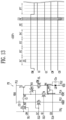
- FIG. 1 is a diagram illustrating an embodiment of a display device according to the disclosure
- FIG. 2 is a circuit diagram illustrating an embodiment of a pixel included in the display device of FIG. 1 ;
- FIG. 3 is a waveform diagram illustrating a method of driving the pixel of FIG. 2 during a display scan period
- FIG. 4 is a diagram illustrating a first period of FIG. 3 together with the pixel of FIG. 2 ;
- FIG. 5 is a diagram illustrating a second period of FIG. 3 together with the pixel of FIG. 2 ;
- FIG. 6 is a diagram illustrating a third period of FIG. 3 together with the pixel of FIG. 2 ;
- FIG. 7 is a diagram illustrating a fourth period of FIG. 3 together with the pixel of FIG. 2 ;
- FIG. 8 is a diagram illustrating a fifth period of FIG. 3 together with the pixel of FIG. 2 ;
- FIG. 9 is a diagram illustrating a sixth period of FIG. 3 together with the pixel of FIG. 2 ;
- FIG. 10 is a diagram illustrating a seventh period of FIG. 3 together with the pixel of FIG. 2 ;
- FIG. 11 is a waveform diagram illustrating a method of driving the pixel of FIG. 2 during a self-scan period
- FIG. 12 is a waveform diagram illustrating a first period to a fifth period of FIG. 11 ;
- FIG. 13 is a waveform diagram illustrating a sixth period of FIG. 11 ;
- FIG. 14 is a waveform diagram illustrating a seventh period of FIG. 11 ;
- FIG. 15 is a diagram illustrating an embodiment of high-speed driving of a display device according to the disclosure.
- FIG. 16 is a diagram illustrating a luminance difference during the high-speed driving and the low-speed driving
- FIG. 17 is a diagram illustrating a G-value corresponding to a width of a fourth scan signal
- FIGS. 18 and 19 are diagrams equivalently illustrating a connection relationship between a light-emitting element and initialization power
- FIGS. 20 A and 20 B are diagrams illustrating a case where a luminance reversal phenomenon occurs in relation to FIG. 19 ;
- FIG. 21 is a diagram illustrating a case where the luminance reversal phenomenon does not occur in relation to FIG. 19 ;
- FIGS. 22 and 23 are diagrams illustrating an embodiment of a supply waveform of a fourth scan signal according to the disclosure.
- FIG. 24 is a diagram illustrating an embodiment of a process of setting a width of a fourth scan signal according to the disclosure.
- FIG. 25 is a diagram illustrating an embodiment of the width of the fourth scan signal corresponding to a driving frequency
- FIG. 26 is a diagram illustrating an embodiment of a display device
- FIG. 27 is a diagram illustrating an embodiment of pixels disposed in the display device of FIG. 26 ;
- FIG. 28 is a diagram illustrating the fourth scan signal corresponding to the embodiment of FIG. 26 ;
- FIG. 29 is a diagram equivalently illustrating a flow of a current during a second time.
- an expression “is the same” in the description may mean “is substantially the same”. That is, the expression “is the same” may be the same enough for those of ordinary skill to understand that it is the same.
- Other expressions may also be expressions in which “substantially” is omitted.
- “About” or “approximately” as used herein is inclusive of the stated value and means within an acceptable range of deviation for the particular value as determined by one of ordinary skill in the art, considering the measurement in question and the error associated with measurement of the particular quantity (i.e., the limitations of the measurement system).
- the term such as “about” can mean within one or more standard deviations, or within ⁇ 30%, 20%, 10%, 5% of the stated value, for example.
- FIG. 1 is a diagram illustrating an embodiment of a display device according to the disclosure.
- a display device 1000 in an embodiment of the disclosure includes a pixel unit 100 , scan drivers 200 , 300 , 400 , and 500 , an emission driver 600 , a data driver 700 , and a timing controller 800 .
- the display device 1000 may further include a power supply for supplying a voltage of first power VDD, a voltage of second power VSS, a voltage of initialization power VINT, and a voltage of reference power VREF to the pixel unit 100 .
- the power supply may supply a gate-on voltage and a gate-off voltage of a scan signal and/or an emission control signal to the scan drivers 200 , 300 , 400 , and 500 and/or the emission driver 600 .
- this is merely one of embodiments, and at least one of the first power VDD, the second power VSS, the initialization power VINT, and the reference power VREF may be supplied from the data driver 700 or the timing controller 800 .
- the first power VDD and the second power VSS may be used to drive a light-emitting element.
- the voltage of the first power VDD may be set to a level higher than that of the voltage of the second power VSS.
- the first power VDD may be a positive voltage and the second power VSS may be a negative voltage, for example.
- the initialization power VINT may be power for initializing a pixel PX.
- a driving transistor included in the pixel PX and an anode electrode of the light-emitting element may be initialized by the voltage of the initialization power VINT, for example.
- the initialization power VINT may be set to a voltage lower than that of a data signal.
- the reference power VREF may be power for initializing the pixel PX.
- a capacitor and/or a transistor included in the pixel PX may be initialized by the voltage of the reference power VREF, for example.
- the reference power VREF may be a positive voltage.
- the reference power VREF may have the same voltage level as the first power VDD, for example, but the disclosure is not limited thereto.
- the display device 1000 may display an image at various image refresh rates (driving frequencies, or screen reproduction rates) according to a driving condition.
- the image refresh rate means a frequency at which the data signal is written to the driving transistor of the pixel PX.
- the image refresh rate may be also referred to as a screen scan rate or a screen reproduction frequency, and may indicate a frequency at which a display screen is reproduced during one second, for example.
- an output frequency of the data driver 700 for one horizontal line (or pixel row) and/or an output frequency of the first scan driver 200 outputting a first scan signal (or write scan signal) may be determined in response to the image refresh rate.
- a refresh rate for driving a moving image may be a frequency of about 60 hertz (Hz) or more (e.g., about 120 Hz, about 240 Hz, or the like), for example.
- the display device 1000 may adjust the output frequency of the scan drivers 200 , 300 , 400 , and 500 for one horizontal line (or pixel row), and the output frequency of the data driving 700 corresponding to the output frequency of the scan drivers 200 , 300 , 400 , and 500 according to the driving condition.
- the display device 1000 may display an image in response to various image refresh rates of 1 Hz to 240 Hz, for example. However, this is merely one of embodiments, and the display device 1000 may display an image also at an image refresh rate of 240 Hz or higher (e.g., 480 Hz).
- the pixel unit 100 includes the pixels PX respectively connected to data lines DL, scan lines SL 1 , SL 2 , SL 3 , and SL 4 , and emission control lines EL.
- the pixels PX may receive the first power VDD, the second power VSS, the initialization power VINT, and the reference power VREF from an outside.
- a pixel PX disposed in an i-th (i is a natural number) row and a j-th (j is a natural number) column may be connected (or coupled) to scan lines SL 1 i , SL 2 i , SL 3 i , and SL 4 i corresponding to an i-th horizontal line, an emission control line ELI corresponding to the i-th horizontal line, and a data line DLj corresponding to a j-th vertical line (or pixel column).
- the signal lines SL 1 , SL 2 , SL 3 , SL 4 , EL, and DL connected to the pixel PX may be set variously in response to a circuit structure of the pixel PX.
- the scan drivers 200 , 300 , 400 , and 500 may be divided into configurations and operations of a first scan driver 200 , a second scan driver 300 , a third scan driver 400 , and a fourth scan driver 500 .
- the division of the scan driver is for convenience of description, and at least some of the scan driver may be integrated into one driving circuit, module, or the like, according to design.
- the first scan driver 200 may supply a first scan signal to first scan lines SL 1 in response to a first driving control signal SCS 1 supplied from the timing controller 800 .
- the first scan driver 200 may sequentially supply the first scan signal to the first scan lines SL 1 , for example.
- the pixels PX may be selected in a horizontal line unit (that is, a pixel row unit), and the data signal may be supplied to the pixels PX. That is, the first scan signal may be a signal used for writing data.
- the first scan signal may be set to a gate-on voltage (e.g., a relatively low level).
- a transistor included in the pixel PX and receiving the first scan signal is set to a turn-on state when the first scan signal is supplied.
- the first scan driver 200 may supply the first scan signal at a frequency equal to the refresh rate of the display device 1000 in response to any one of the first scan lines SL 1 (e.g., an i-th scan line SL 1 i ).
- the first scan driver 200 may supply a scan signal to the first scan lines SL 1 during a display scan period of one frame. In an embodiment, the first scan driver 200 may supply at least one first scan signal to each of the first scan lines SL 1 during the display scan period, for example.
- the second scan driver 300 may supply a second scan signal to second scan lines SL 2 in response to a second driving control signal SCS 2 supplied from the timing controller 800 .
- the second scan driver 300 may sequentially supply the second scan signal to the second scan lines SL 2 , for example.
- the second scan signal may be supplied to initialize the pixels PX and/or to compensate for a threshold voltage (Vth) of the driving transistor.
- the second scan signal may be set to a gate-on voltage (e.g., a relatively low level).
- a transistor included in the pixel PX and receiving the second scan signal is set to a turn-on state when the second scan signal is supplied.
- the second scan driver 300 may supply the second scan signal to the second scan lines SL 2 during the display scan period of one frame. In an embodiment, the second scan driver 300 may supply at least one second scan signal to each of the second scan lines SL 2 during the display scan period, for example.
- the third scan driver 400 may supply a third scan signal to third scan lines SL 3 in response to a third driving control signal SCS 3 supplied from the timing controller 800 .
- the third scan driver 400 may sequentially supply the third scan signal to the third scan lines SL 3 , for example.
- the third scan signal may be supplied to initialize the driving transistor included in the pixels PX.
- the third scan signal may be set to a gate-on voltage (e.g., a relatively low level).
- a transistor included in the pixel PX and receiving the third scan signal is set to a turn-on state when the third scan signal is supplied.
- the third scan driver 400 may supply the third scan signal to the third scan lines SL 3 during the display scan period of one frame. In an embodiment, the third scan driver 400 may supply at least one third scan signal to each of the third scan lines SL 3 during the display scan period, for example.
- the fourth scan driver 500 may supply a fourth scan signal to fourth scan lines SL 4 (or initial scan lines) in response to a fourth driving control signal SCS 4 supplied from the timing controller 800 .
- the fourth scan driver 500 may sequentially supply the fourth scan signal to the fourth scan lines SL 4 .
- the fourth scan signal may be supplied to initialize the light-emitting element included in the pixels PX, for example.
- the fourth scan signal may be set to a gate-on voltage (e.g., a relatively low level).
- a transistor included in the pixel PX and receiving the fourth scan signal is set to a turn-on state when the fourth scan signal is supplied.
- the fourth scan driver 500 may supply the fourth scan signal at a constant frequency regardless of the image refresh rate frequency of the display device 1000 in response to one (e.g., SL 4 i ) of the fourth scan lines SL 4 .
- the fourth scan driver 500 may perform scanning once (supply at least one fourth scan signal) during the display scan period, and perform scanning at least once according to the image refresh rate during the self-scan period, for example.
- the number of repetitions of an operation of the fourth scan driver 500 supplying the fourth scan signal to each of the fourth scan lines SL 4 within one frame period may be increased.
- the emission driver 600 may supply an emission control signal to the emission control lines EL in response to a fifth driving control signal ECS supplied from the timing controller 800 .
- the emission driver 600 may sequentially supply the emission control signal to the emission control lines EL, for example.
- the emission control signal When the emission control signal is supplied, electrical connection between the driving transistor included and the light-emitting element in each of the pixels PX may be blocked. To this end, the emission control signal may be set to a gate-off voltage (e.g., a relatively high level) so that the transistor included in the pixels PX may be turned off. A transistor included in the pixel PX and receiving the emission control signal may be turned off when the emission control signal is supplied, and may be turned on in other cases.
- the emission control signal may be used to control an emission time of the pixels PX. To this end, the emission control signal may be set to a width greater than that of the scan signal.
- the emission driver 600 may supply the emission control signal at a constant frequency regardless of the image refresh rate frequency, similarly to the fourth scan driver 500 . Therefore, within one frame period, the emission control signal supplied to the emission control lines EL may be repeatedly supplied at a predetermined period. Accordingly, when the image refresh rate is decreased, the number of repetitions of an operation of the emission driver 600 supplying the emission control signal to each of the emission control lines EL may be increased within one frame period.
- the data driver 700 may receive a sixth driving control signal DCS and image data (also referred to as digital image data) RGB from the timing controller 800 .
- the data driver 700 may supply the data signal to the data lines DL in response to the sixth driving control signal DCS.
- the data driver 700 may generate an analog data signal using the digital image data RGB and supply the generated data signal to the data lines DL in synchronization with the first scan signal, for example.
- the timing controller 800 may generate the first driving control signal SCS 1 , the second driving control signal SCS 2 , the third driving control signal SCS 3 , the fourth driving control signal SCS 4 , the fifth driving control signal ECS, and the sixth driving control signal DCS in response to synchronization signals supplied from the outside.
- the timing controller 800 may rearrange input image data supplied from the outside into the image data RGB and supply the rearranged image data to the data driver 700 .
- the first driving control signal SCS 1 may include a first scan start pulse and clock signals.
- the first scan start pulse may control a first timing of the first scan signal output from the first scan driver 200 .
- the clock signals may be used to shift the first scan start pulse.
- the second driving control signal SCS 2 may include a second scan start pulse and clock signals.
- the second scan start pulse may control a first timing of the second scan signal output from the second scan driver 300 .
- the clock signals may be used to shift the second scan start pulse.
- the third driving control signal SCS 3 may include a third scan start pulse and clock signals.
- the third scan start pulse may control a first timing of the third scan signal output from the third scan driver 400 .
- the clock signals may be used to shift the third scan start pulse.
- the fourth driving control signal SCS 4 may include a fourth scan start pulse and clock signals.
- the fourth scan start pulse may control a first timing of the fourth scan signal output from the fourth scan driver 500 .
- the clock signals may be used to shift the fourth scan start pulse.
- the fifth driving control signal ECS may include an emission start pulse and clock signals.
- the emission start pulse may control a first timing of the emission control signal output from the emission driver 600 .
- the clock signals may be used to shift the emission start pulse.
- the sixth driving control signal DCS may include a source start pulse and clock signals.
- the source start pulse may control a sampling start time point of data.
- the clock signals may be used to control a sampling operation.
- FIG. 2 is a circuit diagram illustrating an embodiment of the pixel included in the display device of FIG. 1 .
- a pixel PX disposed on an i-th horizontal line and a j-th vertical line is shown.
- a pixel PX in an embodiment of the disclosure may include a light-emitting element LD and a pixel circuit that controls a current amount flowing through the light-emitting element LD.
- the light-emitting element LD may be connected between a first power line PL 1 to which the first power VDD is supplied and a second power line PL 2 to which the second power VSS is supplied.
- a first electrode (e.g., an anode electrode) of the light-emitting element LD may be connected to the first power line PL 1 via a fourth node N 4 and the pixel circuit
- a second electrode (e.g., a cathode electrode) of the light-emitting element LD may be connected to the second power line PL 2 .
- the light-emitting element LD may emit light with a luminance corresponding to a driving current supplied from the pixel circuit.
- the voltage of the first power VDD and the voltage of the second power VSS may have a predetermined potential difference so that the light-emitting element LD may emit light.
- the first power VDD may be high-potential power having a higher voltage
- the second power VSS may be lower-potential power having a voltage lower than that of the first power VDD, for example.
- the light-emitting element LD may be selected as an organic light-emitting diode (“OLED”).
- the light-emitting element LD may be selected as an inorganic light-emitting diode such as a micro light-emitting diode (“LED”) or a quantum dot light-emitting diode.
- the light-emitting element LD may be an element configured of a combination of an organic material and an inorganic material.
- the pixel PX includes a single light-emitting element LD, but in another embodiment, the pixel PX may include a plurality of light-emitting elements, and the plurality of light-emitting elements may be connected to each other in series, in parallel, or in series and parallel.
- the pixel circuit may include at least one transistor and at least one capacitor.
- the pixel circuit includes a first transistor T 1 (or a driving transistor), a second transistor T 2 , a third transistor T 3 , a fourth transistor T 4 , a fifth transistor T 5 , a sixth transistor T 6 , a seventh transistor T 7 , a first capacitor C 1 , and a second capacitor C 2 , for example.
- the first to seventh transistors T 1 to T 7 are shown as P-type transistors, but the disclosure is not limited thereto. In an embodiment, at least one of the first to seventh transistors T 1 to T 7 may be formed as an N-type transistor, for example.
- a first electrode of the first transistor T 1 is connected to the first power line PL 1 , and a second electrode is connected to a third node N 3 .
- a gate electrode of the first transistor T 1 is connected to a first node N 1 .
- the first transistor T 1 may control a current amount flowing from the first power line PL 1 (that is, the first power VDD) to the second power line PL 2 (that is, the second power VSS) via the light-emitting element LD in response to a voltage of the first node N 1 .
- the first transistor T 1 may be also referred to as a driving transistor.
- a first electrode of the second transistor T 2 is connected to the data line DLj, and a second electrode is connected to a second node N 2 .
- a gate electrode of the second transistor T 2 is connected to the first scan line SL 1 .
- the second transistor T 2 is turned on when a first scan signal GW is supplied to electrically connect the data line DLj and the second node N 2 .
- the first scan signal GW may be also referred to as a write scan signal
- the second transistor T 2 may be also referred to as a switching transistor.
- a first electrode of the third transistor T 3 is connected to the third node N 3 , and a second electrode is connected to the first node N 1 .
- a gate electrode of the third transistor T 3 is connected to the second scan line SL 2 .
- the third transistor T 3 is turned on when a second scan signal GC is supplied to the second scan line SL 2 to electrically connect the first node N 1 and the third node N 3 .
- the first transistor T 1 is connected in a diode form.
- the second scan signal GC may be also referred to as a compensation scan signal
- the third transistor T 3 may be also referred to as a compensation transistor.
- a first electrode of the fourth transistor T 4 is connected to the first node N 1 , and a second electrode is connected to a fourth power line PL 4 to which the initialization power VINT is supplied.
- a gate electrode of the fourth transistor T 4 is connected to the third scan line SL 3 .
- the fourth transistor T 4 is turned on when a third scan signal GI is supplied to the third scan line SL 3 to supply the voltage of the initialization power VINT to the first node N 1 .
- the third scan signal GI may be also referred to as a second initialization scan signal
- the fourth transistor T 4 may be also referred to as a second initialization transistor
- the fourth power line PL 4 may be also referred to as a first initialization power line.
- a first electrode of the fifth transistor T 5 is connected to the second node N 2 , and a second electrode is connected to the third power line PL 3 .
- a gate electrode of the fifth transistor T 5 is connected to the second scan line SL 2 .
- the fifth transistor T 5 is turned on when the second scan signal GC is supplied to the second scan line SL 2 to supply the voltage of the reference voltage VREF to the second node N 2 .
- the reference power VREF may be set to the same voltage as the first power VDD or a predetermined direct current (“DC”) voltage.
- the fifth transistor T 5 may be also referred to as a third initialization transistor, and the third power line PL 3 may be also referred to as a second initialization power line.
- a first electrode of the sixth transistor T 6 is connected to the third node N 3 , and a second electrode is connected to the fourth node N 4 (that is, the anode electrode of the light-emitting element LD).
- a gate electrode of the sixth transistor T 6 is connected to the emission control line EL.
- the sixth transistor T 6 is turned off when the emission control signal EM having an inactive level (e.g., high level) is supplied to the emission control line EL, and turned on in other cases.
- the first transistor T 1 and the light-emitting element LD are electrically cut off, and thus the light-emitting element LD may be set to a non-emission state.
- the sixth transistor T 6 may be also referred to as an emission transistor.
- a first electrode of the seventh transistor T 7 is connected to the fourth node N 4 , and a second electrode is connected to the fourth power line PL 4 .
- a gate electrode of the seventh transistor T 7 is connected to the fourth scan line SL 4 .
- the seventh transistor T 7 is turned on when a fourth scan signal GB is supplied to the fourth scan line SL 4 to supply the voltage of the initialization power VINT to the anode electrode of the light-emitting element LD.
- a voltage of an organic capacitor Cle formed in the light-emitting element LD may be discharged.
- black expression capability may be improved.
- the fourth scan signal GB may be also referred to as a first initialization scan signal (or an initialization scan signal)
- the seventh transistor T 7 may be also referred to as a first initialization transistor (or an initialization transistor).
- the first capacitor C 1 is connected between the first node N 1 and the second node N 2 .
- the first capacitor C 1 may store a voltage between the first node N 1 and the second node N 2 .
- the second capacitor C 2 is connected between the first power line PL 1 and the second node N 2 .
- the second capacitor C 2 may store a voltage of the second node N 2 and may stabilize the voltage of the second node N 2 .
- FIG. 3 is a waveform diagram illustrating a method of driving the pixel of FIG. 2 during the display scan period.
- the display scan period DSP may include a first period P 1 to a fourth period P 4 .
- the first period P 1 to the fourth period P 4 may be a threshold voltage compensation period of the first transistor T 1 .
- the display scan period DSP may include a fifth period P 5 and a sixth period P 6 .
- the fifth period P 5 may be a data writing period
- the sixth period P 6 may be an initialization period of the light-emitting element LD.
- the display scan period DSP may include a seventh period P 7 .
- the seventh period P 7 may be an emission period.
- An interval between dotted lines in FIG. 3 may be set to one horizontal period (1H).
- One horizontal period (1H) may refer to a time interval of sequentially supplied scan signals or may be a time allocated to apply a data signal to one horizontal line.
- one horizontal period (1H) may be approximately 1.84 microseconds ( ⁇ s) or less, for example.
- the first period P 1 to the fourth period P 4 are shown as having a length of three horizontal periods (3H), but may have a value greater than or less than three horizontal periods (3H) according to a driving method. In addition, a length of at least one of the first period P 1 to the fourth period P 4 may be different from that of other periods.
- FIG. 4 is a diagram illustrating the first period of FIG. 3 together with the pixel of FIG. 2 .
- the emission control signal EM having the inactive level (e.g., high level) is supplied to the emission control line EL during the first period P 1 to the sixth period P 6 .
- the emission control signal EM having the inactive level (e.g., high level) is supplied to the emission control line EL
- the sixth transistor T 6 is turned off.
- electrical connection between the first transistor T 1 and the light-emitting element LD is blocked, and thus the light-emitting element LD is set to the non-emission state.
- the third scan signal GI is supplied to the third scan line SL 3 .
- the fourth transistor T 4 is turned on.
- the voltage of the initialization power VINT is supplied to the first node N 1 , and a voltage of a data signal of a previous frame may be decreased.
- FIG. 5 is a diagram illustrating the second period of FIG. 3 together with the pixel of FIG. 2 .
- the second scan signal GC is supplied to the second scan line SL 2 .
- the third transistor T 3 and the fifth transistor T 5 are turned on.
- the third transistor T 3 When the third transistor T 3 is turned on, the first transistor T 1 is connected in a diode form. Then, a voltage corresponding to a difference between the first power VDD and the threshold voltage of the first transistor T 1 may be applied to the first node N 1 .
- the fifth transistor T 5 When the fifth transistor T 5 is turned on, the voltage of the reference power VREF is supplied to the second node N 2 . Then, a voltage of the second node N 2 is changed from a voltage of the previous frame to approximately the voltage of the reference power VREF.
- the first capacitor C 1 may store a voltage corresponding to a difference between the first node N 1 and the second node N 2 .
- the first power VDD and the reference power VREF are set to a fixed voltage, a voltage corresponding to the threshold voltage of the first transistor T 1 may be stored in the first capacitor C 1 .
- FIG. 6 is a diagram illustrating the third period of FIG. 3 together with the pixel of FIG. 2 .
- the pixel PX may be driven in a method identical or similar to that of the first period P 1 described above.
- the third scan signal GI is supplied to the third scan line SL 3 .
- the fourth transistor T 4 is turned on.
- the voltage of the initialization power VINT is supplied to the first node N 1 .
- the voltage of the first node N 1 may be determined regardless of the voltage applied in the previous frame.
- FIG. 7 is a diagram illustrating the fourth period of FIG. 3 together with the pixel of FIG. 2 .
- the pixel PX may be driven in a method identical or similar to that of the method of the second period P 2 described above.
- the second scan signal GC is supplied to the second scan line SL 2 .
- the third transistor T 3 and the fifth transistor T 5 are turned on.
- the third transistor T 3 When the third transistor T 3 is turned on, the first transistor T 1 is connected in a diode form. Then, the voltage corresponding to the difference between the first power VDD and the threshold voltage of the first transistor T 1 may be applied to the first node N 1 .
- the fifth transistor T 5 When the fifth transistor T 5 is turned on, the voltage of the reference power VREF is supplied to the second node N 2 . Then, the voltage of the second node N 2 is changed to approximately the voltage of the reference power VREF. During the fourth period P 4 , the voltage corresponding to the threshold voltage of the first transistor T 1 may be stored in the first capacitor C 1 .
- the threshold voltage of the first transistor T 1 may be more accurately compensated through the first period P 1 to the fourth period P 4 .
- the first period P 1 to the fourth period P 4 are included in order to compensate for the threshold voltage, but the disclosure is not limited thereto.
- a plurality of additional periods may be further included in addition to the first period P 1 to the fourth period P 4 to compensate for the threshold voltage, for example.
- FIG. 8 is a diagram illustrating the fifth period of FIG. 3 together with the pixel of FIG. 2 .
- the first scan signal GW is supplied to the first scan line SL 1 .
- the second transistor T 2 is turned on.
- the data signal from the data line DLj is supplied to the second node N 2 .
- the voltage of the second node N 2 is changed from the voltage of the reference power VREF to the voltage of the data signal.
- the voltage of the first node N 1 is changed corresponding to a voltage change amount of the second node N 2 by coupling of the first capacitor C 1 .
- the voltage of the first node N 1 may be changed by a voltage corresponding to a difference between the voltage of the data signal and the reference power VREF, for example.
- the voltage applied to the first node N 1 may be determined by the voltage of the data signal.
- the second capacitor C 2 stores the voltage of the data signal applied to the second node N 2 .
- the fifth period P 5 in which the voltage of the data signal is input does not overlap the first period P 1 to the fourth period P 4 in which the threshold voltage is compensated. Therefore, even though the fifth period P 5 (or one horizontal period) in which the voltage of the data signal is input is shortened, a threshold voltage compensation period (that is, the first period P 1 to the fourth period P 4 ) may be sufficiently secured. Therefore, the display device 1000 of the disclosure may implement a display device of high-resolution and display an image at a relatively high scan rate (or driving frequency).
- FIG. 9 is a diagram illustrating the sixth period of FIG. 3 together with the pixel of FIG. 2 .
- the fourth scan signal GB is supplied to the fourth scan line SL 4 .
- the seventh transistor T 7 is turned on.
- the voltage of the initialization power VINT may be supplied to the fourth node N 4 .
- a charged voltage of the organic capacitor Cle may be discharged.
- FIG. 10 is a diagram illustrating the seventh period of FIG. 3 together with the pixel of FIG. 2 .
- the seventh period P 7 supply of the emission control signal EM having the inactive level (e.g., high level) to the emission control line EL is stopped.
- the sixth transistor T 6 is turned on.
- the seventh period P 7 may be also referred to as an emission period.
- FIG. 11 is a waveform diagram illustrating a method of driving the pixel of FIG. 2 during the self-scan period.
- the self-scan period SSP is a period in which an image is displayed again without switching a frame as a period in which light is emitted while maintaining a voltage of a previously supplied data signal.
- one frame may include one display scan period DSP and one or more self-scan periods SSP.
- One or more self-scan periods SSP may be successively disposed after the display scan period DSP.
- the threshold voltage compensation operation and the data writing operation are omitted in the self-scan period SSP, and an operation of initializing the light-emitting element LD and an emission operation may be performed.
- the self-scan period SSP may be set to the same length as the display scan period DSP.
- the self-scan period SSP may include a first period P 1 ′ to a seventh period P 7 ′.
- FIG. 12 is a waveform diagram illustrating the first period to the fifth period of FIG. 11 .
- the emission control signal EM having the inactive level (e.g., high level) is supplied to the emission control line EL in the first period P 1 ′ to the fifth period P 5 ′.
- the emission control signal EM having the inactive level (e.g., high level) is supplied to the emission control line EL
- the sixth transistor T 6 is turned off.
- electrical connection between the first transistor T 1 and the light-emitting element LD is blocked, and thus the light-emitting element LD is set to the non-emission state.
- the scan signals GW, GC, GI, and GB are not supplied to the scan lines SL 1 to SL 4 . Accordingly, during the first period P 1 ′ to the fifth period P 5 ′, the second transistor T 2 , the third transistor T 3 , the fourth transistor T 4 , the fifth transistor T 5 , and the seventh transistor T 7 are set to a turn-off state.
- FIG. 13 is a waveform diagram illustrating the sixth period of FIG. 11 .
- the fourth scan signal GB is supplied to the fourth scan line SL 4 .
- the seventh transistor T 7 is turned on.
- the voltage of the initialization power VINT may be supplied to the fourth node N 4 .
- the charged voltage of the organic capacitor Cle may be discharged.
- FIG. 14 is a waveform diagram illustrating the seventh period of FIG. 11 .
- the seventh period P 7 ′ the supply of the emission control signal EM having the inactive level (e.g., high level) to the emission control line EL is stopped.
- the sixth transistor T 6 is turned on.
- the first transistor T 1 and the light-emitting element LD are electrically connected.
- the first transistor T 1 supplies the driving current corresponding to the voltage of the first node N 1 to the second power VSS via the first power VDD, the sixth transistor T 6 , and the light-emitting element LD.
- the light-emitting element LD generates light of a luminance corresponding to the driving current.
- the display device 1000 may be driven at various driving frequencies (various frame frequencies) because one frame includes the display scan period DSP and the self-scan period SSP.
- FIG. 15 is a diagram illustrating an embodiment of high-speed driving of a display device according to the disclosure.
- one frame 1 FRAME may include one display scan period DSP and one self-scan period SSP.
- a frequency of the high-speed driving may be set to 240 Hz, for example, but the disclosure is not limited thereto.
- each of the display scan period DSP and the self-scan period SSP may be 480 Hz. That is, in an embodiment of the disclosure, an image may be displayed by driving the display scan period DSP and the self-scan period SSP at a frequency higher than the driving frequency.
- FIG. 15 illustrates peak luminances PLM 1 and PLM 2 of the display scan period DSP and the self-scan period SSP when the same data signal is successively supplied during 10 frame periods.
- a first peak luminance PLM 1 is displayed in the display scan period DSP, and a second peak luminance PLM 2 higher than the first peak luminance PLM 1 is displayed in the self-scan period SSP.
- Such a luminance difference may be caused by a characteristic change of the first transistor T 1 due to the first power VDD supplied to the first electrode of the first transistor T 1 during the first period P 1 ′ to the fourth period P 4 ′ of the self-scan period SSP.
- the luminance difference may be caused by a characteristic change due to a leakage current from the first node N 1 .
- the luminance difference due to the display scan period DSP and the self-scan period SSP may occur due to the characteristic change (or hysteresis) of the first transistor T 1 during the self-scan period SSP and/or the leakage current from the first node N 1 , and thus a desired luminance may not be implemented in the pixel PX.
- FIG. 16 is a diagram illustrating a luminance difference during the high-speed driving and the low-speed driving.
- a frequency of the high-speed driving may be set to 240 Hz, and a frequency of the low-speed driving may be set to 60 Hz, in an embodiment.
- the drawing of FIG. 16 is a case where that the same data signal is supplied during the high-speed driving and the low-speed driving.
- one frame may include one display scan period DSP and one self-scan period SSP.
- one frame may include one display scan period DSP and seven self-scan periods SSP.
- one frame may display the first peak luminance PLM 1 and the second peak luminance PLM 2 .
- the first peak luminance PLM 1 may be displayed during the display scan period DSP of one frame, and the second peak luminance PLM 2 may be displayed during the self-scan period SSP after the display scan period DSP.
- a peak luminance may gradually increase, and then a k-th (here, “k” is a natural number equal to or greater than 3) peak luminance PLMk may be displayed during a last self-scan period SSP.
- the k-th peak luminance PLMk is set to a luminance higher than that of the second peak luminance PLM 2 .
- seven self-scan periods SSP may be included in one frame during the low-speed driving, and one self-scan period SSP may be included in one frame during the high-speed driving.
- a luminance displayed during the high-speed driving and a luminance displayed during the low-speed driving may be set differently during the same time.
- FIG. 17 is a diagram illustrating a G-value corresponding to a width of the fourth scan signal.
- the G-value may be a value obtained by dividing a value obtained by subtracting a luminance of a lowest frequency (Lum(minfreq)) from a luminance of a highest frequency (Lum(maxfreq)) by the luminance of the highest frequency (Lum(maxfreq)) (e.g., Lum(maxfreq) ⁇ Lum(minfreq))/Lum(maxfreq)) and may be used as an authentication specification of the display device 1000 of which a frequency is changed.
- Lum(minfreq) lowest frequency
- Lum(maxfreq) the luminance of the highest frequency
- H-GB means the fourth scan signal GB supplied during the self-scan period SSP
- 11G, 23G, 35G, 51G, 87G, 127G, 151G, 203G, 255G, or the like means displayed grayscales.
- a portion displayed with a dotted line indicates a section included in a G-value specification.
- the specification of the G-value may be set differently for each company.
- the fourth scan signal GB may be included in the G-value specification at a relatively high grayscale (e.g., 23 grayscales (23G) or higher) (e.g., a G-value is stably maintained).
- a relatively high grayscale e.g., 23 grayscales (23G) or higher
- Being included in the G-value specification may mean that a luminance difference does not largely occur during the high-speed driving and the low-speed driving, and thus the luminance difference is not recognized by a user.
- the G-value largely changes in response to the width of the fourth scan signal GB.
- the width of the fourth scan signal GB is set to be wide (e.g., a width of 1.4 ⁇ s or more) when implementing the relatively low grayscale, the G-Value may be included in the specification, and thus a desired luminance may be implemented during the high-speed driving and the low-speed driving.
- the G-value is not included in the specification, and thus a luminance difference may occur during the high-speed driving and the low-speed driving.
- the luminance difference may be recognized by the user during the high-speed driving and the low-speed driving.
- the width of the fourth scan signal GB is desired to be set sufficiently wide to satisfy the G-value specification during the high-speed driving and the low-speed driving.
- the width of the fourth scan signal GB may be set greater than one horizontal period (1H). That is, in an embodiment of the disclosure, the width of the fourth scan signal GB may be set greater than one horizontal period (1H) and shorter than two horizontal periods (2H).
- FIGS. 18 and 19 are diagrams equivalently illustrating a connection relationship between the light-emitting element and the initialization power.
- resistors R 1 , R 2 , R 3 , and R 4 equivalently indicate a resistance of a line and a transistor (e.g., T 7 ).
- FIG. 18 illustrates a case where the fourth scan signal GB has a width within one horizontal period (1H), and thus the fourth scan signal GB supplied to the i-th horizontal line does not overlap the fourth scan signal GB supplied to an (i+1)-th horizontal line.
- FIG. 19 illustrates a case where the fourth scan signal GB has a width exceeding one horizontal period (1H), and thus the fourth scan signal GB supplied to the i-th horizontal line overlaps the fourth scan signal GB supplied to the (i+1)-th horizontal line. Thereafter, a period in which the fourth scan signal GB supplied to the i-th horizontal line and the fourth scan signal GB supplied to the (i+1)-th horizontal line are simultaneously supplied is also referred to as an overlap period.
- the seventh transistor T 7 disposed on a corresponding horizontal line is turned on. Then, the anode electrode of the light-emitting element LD and the fourth power line PL 4 are electrically connected, and thus the anode electrode of the light-emitting element LD disposed on the i-th horizontal line may be initialized.
- the seventh transistor T 7 disposed on the corresponding horizontal line is turned on. Then, the anode electrode of the light-emitting element LD and the fourth power line PL 4 are electrically connected, and thus the anode electrode of the light-emitting element LD disposed on the i-th horizontal line may be initialized.
- the fourth scan signal GB is supplied to the (i+1)-th horizontal line during a partial period (that is, the overlap period) of a period in which the fourth scan signal GB is supplied to the i-th horizontal line.
- the seventh transistor T 7 disposed on the (i+1)-th horizontal line is turned on.
- the anode electrode of an (i+1)-th light-emitting element LD and the fourth power line PL 4 are electrically connected.
- the anode electrode of the light-emitting element LD disposed on the (i+1)-th horizontal line is electrically connected to the anode electrode of the light-emitting element LD disposed on the i-th horizontal line.
- a voltage of the anode electrode of the light-emitting element LD disposed on the i-th horizontal line may temporarily increase, and thus a luminance reversal phenomenon may occur.
- FIGS. 20 A and 20 B are diagrams illustrating a case where the luminance reversal phenomenon occurs in relation to FIG. 19 .
- FIG. 21 is a diagram illustrating a case where the luminance reversal phenomenon does not occur in relation to FIG. 19 .
- FIG. 20 A illustrates a case where the overlap period is short
- FIG. 20 B is a diagram illustrating a luminance of the light-emitting element corresponding to the overlap period of FIG. 20 A .
- an i-th fourth scan signal GBi and an (i+1)-th fourth scan signal GBi+1 may be simultaneously supplied during the overlap period.
- an anode electrode voltage of the light-emitting element LD disposed on the (i+1)-th horizontal line is supplied to the anode electrode of the light-emitting element LD disposed on the i-th horizontal line as shown in FIG. 20 , and thus an anode electrode voltage of the light-emitting element LD disposed on the i-th horizontal line is increased.
- the anode electrode voltage of the light-emitting element LD disposed on the i-th horizontal line may be increased and then may not be discharged, and thus the luminance of the light-emitting element LD disposed on the i-th horizontal line may be increased.
- the i-th fourth scan signal GBi and the (i+1)-th fourth scan signal GBi+1 may be simultaneously supplied during the overlap period.
- the voltage of the light-emitting element LD disposed on the i-th horizontal line temporarily is increased and then is decreased due to the voltage of the initialization power VINT. That is, when the overlap period is set to be relatively long, the luminance reversal phenomenon as shown in FIG. 20 B may not occur, and thus a desired luminance may be stably implemented.
- the voltage of the light-emitting element LD may be decreased to the voltage of the initialization power VINT, and thus an image of a uniform luminance may be implemented during the display scan period DSP and self-scan period SSP.
- the overlap period of the fourth scan signal GB is sufficiently long, the luminance reversal phenomenon of the light-emitting element LD may be prevented.
- the fourth scan signal GB does not overlap, the luminance reversal phenomenon does not occur.
- the G-value specification may be satisfied, and thus the luminance difference may be minimized during the high-speed driving and the low-speed driving.
- a method capable of preventing the luminance reversal phenomenon while setting the overlap period of the fourth scan signal GB sufficiently wide using such a characteristic is proposed.
- FIGS. 22 and 23 are diagrams illustrating an embodiment of a supply waveform of a fourth scan signal according to the disclosure.
- GSP may mean a fourth scan start pulse (hereinafter referred to as a “scan start pulse”) included in the fourth driving control signal SCS 4 (refer to FIG. 1 ), and clock signals CLK 1 , CLK 2 , CLK 3 , and CLK 4 may mean clock signals included in the fourth driving control signal SCS 4 .
- a configuration of a stage generating the scan signal (that is, the fourth scan signal GB) while shifting the scan start pulse GSP using the clock signals CLK 1 to CLK 4 is currently known variously.
- a configuration of a stage included in the fourth scan driver 500 and shifting the scan start pulse GSP using the clock signals CLK 1 to CLK 4 may be set to any one of various currently known configurations.
- the first clock signal CLK 1 , the third clock signal CLK 3 , the second clock signal CLK 2 , and the fourth clock signal CLK 4 may be sequentially supplied.
- the first clock signal CLK 1 , the third clock signal CLK 3 , the second clock signal CLK 2 , and the fourth clock signal CLK 4 may have the same period and may be supplied so that a phase is shifted.
- the first clock signal CLK 1 and the third clock signal CLK 3 are supplied to overlap with each other during a first time TI 1
- the second clock signal CLK 2 and the fourth clock signal CLK 4 are supplied to overlap with each other during the first time TI 1 .
- the first clock signal CLK 1 and the fourth clock signal CLK 4 do not overlap
- the second clock signal CLK 2 and the third clock signal CLK 3 do not overlap.
- the second clock signal CLK 2 , the fourth clock signal CLK 4 , the first clock signal CLK 1 , and the third clock signal CLK 3 may be sequentially output as the fourth scan signal GB.
- the i-th fourth scan signal GBi overlaps an (i ⁇ 1)-th fourth scan signal GBi ⁇ 1 and does not overlap (i+1)-th fourth scan signal GBi+1.
- the i-th fourth scan signal GBi may overlap the (i ⁇ 1)-th fourth scan signal GBi ⁇ 1 during the first time TI 1 , for example.
- the (i+1)-th fourth scan signal GBi+1 may not overlap the i-th fourth scan signal GBi and may overlap an (i+2)-th fourth scan signal GBi+2 during the first time TI 1 .
- the fourth scan signal GB may be supplied as shown in FIG. 23 in response to the clock signals CLK 1 to CLK 4 .
- the fourth scan signal supplied to a predetermined fourth scan line overlaps any one of the fourth scan signal supplied first and the fourth scan signal supplied later, and does not overlap the other one.
- the i-th fourth scan signal GBi may overlap the (i ⁇ 1)-th fourth scan signal GBi ⁇ 1 during the first time TI 1 which is a sufficiently long time, and thus the G-value may be satisfied without the luminance reversal phenomenon.
- the (i+1)-th fourth scan signal(GBi+1) may be supplied during a sufficiently long time without overlapping the i-th fourth scan signal GBi, and thus may satisfy the G-value without the luminance reversal phenomenon.
- the width of the fourth scan signal may be set differently according to the driving frequency.
- FIG. 24 is a diagram illustrating an embodiment of a process of setting a width of a fourth scan signal according to the disclosure.
- FIG. 25 is a diagram illustrating an embodiment of the width of the fourth scan signal corresponding to the driving frequency.
- the timing controller 800 sets a frequency at which the display device 1000 is driven.
- the timing controller 800 may drive the display device 1000 at a first frequency (S 242 ), for example.
- the timing controller 800 sets the width of the fourth scan signal GB in response to the corresponding frequency (S 244 ).
- the timing controller 800 may set the width of the fourth scan signal GB to have a first width W 11 at a high-speed driving frequency (that is, a relatively high driving frequency).
- the timing controller 800 may set the width of the fourth scan signal GB greater as the driving frequency is decreased.
- the fourth scan signal GB may be set to have a second width W 12 greater than the first width W 11 , and at a relatively low driving frequency, the fourth scan signal GB may be set to have a third width W 13 greater than the second width W 12 , for example.
- the fourth scan signal supplied to the predetermined fourth scan line may be supplied so as to overlap any one of the fourth scan signal supplied first and the fourth scan signal supplied later and so as not to overlap the other one.
- the timing controller 800 may supply the driving control signals SCS 1 , SCS 2 , SCS 3 , SCS 4 , ECS, and DCS corresponding thereto to the scan drivers 200 , 300 , 400 , and 500 , the emission driver 600 , and the data driver 700 , respectively. Then, a predetermined image may be displayed at the first frequency in the pixel unit 100 .
- the timing controller 800 determines whether the driving frequency of the display device 1000 is changed (S 246 ). When the driving frequency is not changed in operation S 246 , the timing controller 800 drives the display device 1000 at the first frequency (S 247 ).
- the timing controller 800 may set the width of the fourth scan signal GB to correspond to the changed driving frequency (S 248 ), and supply the driving control signals SCS 1 , SCS 2 , SCS 3 , SCS 4 , ECS, and DCS corresponding thereto to the scan drivers 200 , 300 , 400 , and 500 , the emission driver 600 , and the data driver 700 , respectively. Then, a predetermined image may be displayed at the changed frequency in the pixel unit 100 .
- the width of the fourth scan signal GB is shown as the first width W 11 , the second width W 12 , and the third width W 13 in response to the driving frequency, but the disclosure is not limited thereto.
- the fourth scan signal GB may be set to have at least two different widths in response to the driving frequency, for example.
- FIG. 26 is a diagram illustrating an embodiment of a display device.
- FIG. 27 is a diagram illustrating an embodiment of pixels disposed in the display device of FIG. 26 .
- FIGS. 26 and 27 When describing FIGS. 26 and 27 , the same reference numerals are assigned to the same configurations as those in FIG. 1 , and a repetitive description is omitted.
- a display device 1000 a in an embodiment of the disclosure includes a pixel unit 100 a , the scan drivers 200 , 300 , 400 , and 500 , the emission driver 600 , the data driver 700 , and the timing controller 800 .
- the display device 1000 a may include a power supply for supplying the voltage of the first power VDD, the voltage of the second power VSS, a voltage of first initialization power VINT 1 , a voltage of second initialization power VINT 2 , and the voltage of the reference power VREF to the pixel unit 100 a.
- the voltage of the first initialization power VINT 1 may be supplied to a first power line PL 11
- the voltage of the second initialization power VINT 2 may be supplied to a second power line PL 12
- the first power line PL 11 may be electrically connected to pixels PXo (or first pixels) disposed on an odd-numbered (or even-numbered) horizontal line
- the second power line PL 12 may be electrically connected to pixels PXe (or second pixels) disposed on an even-numbered (or odd-numbered) horizontal line.
- the first power line PL 11 and the second power line PL 12 are not electrically connected to each other.
- the first initialization power VINT 1 may be set to the same voltage value as the second initialization power VINT 2 .
- a light-emitting element LD (or a first light-emitting element) of the pixel PXo disposed on the odd-numbered horizontal line may be connected to the first power line PL 11 via the seventh transistor T 7 (or the first initialization transistor).
- a light-emitting element LD (or a second light-emitting element) of the pixel PXe disposed on the even-numbered horizontal line may be connected to the second power line PL 12 via the seventh transistor T 7 (or the second initialization transistor).
- the luminance reversal phenomenon does not occur regardless of the overlap period of the fourth scan signal GB.
- FIG. 28 is a diagram illustrating the fourth scan signal corresponding to the embodiment of FIG. 26 .
- FIG. 29 is a diagram equivalently illustrating a flow of a current during a second time.
- the fourth scan signal overlaps the previously supplied fourth scan signal during a second time TI 2 .
- the second time TI 2 may be experimentally set so that the display device 1000 satisfies the G-value.
- the i-th fourth scan signal GBi may overlap the (i ⁇ 1)-th fourth scan signal GBi ⁇ 1 during the second time TI 2 , for example.
- the (i+1)-th fourth scan signal GBi+1 may overlap the i-th fourth scan signal GBi during the second time TI 2 .
- the second time TI 2 is set to a relatively short time, the luminance reversal phenomenon does not occur.
- the pixels PXo disposed on the odd-numbered (or even-numbered) horizontal line receive the first initialization power VINT 1 from the first power line PL 11
- the pixels PXe disposed on the even-numbered (or odd-numbered) horizontal line receive the second initialization power VINT 2 from the second power line PL 12 .
- a seventh transistor T 7 disposed on the i-th horizontal line is turned on. Then, a light-emitting element LD disposed on the i-th horizontal line is electrically connected to the first power line PL 11 and initialized by a voltage of the first initialization power VINT 1 supplied from the first power line PL 11 .
- a seventh transistor T 7 disposed on the (i+1)-th horizontal line is turned on.
- a light-emitting element LD disposed on the (i+1)-th horizontal line is initialized by a voltage of the second initialization power VINT 2 supplied from the second power line PL 12 .
- resistors R 4 and R 5 equivalently indicate a resistance of the (i+1)-th horizontal line.
- the i-th fourth scan signal GBi and the (i+1)-th fourth scan signal GBi+1 overlap, the light-emitting element LD disposed on the (i+1)-th horizontal line and the light-emitting element LD disposed on the i-th horizontal line are not electrically connected, and thus the luminance reversal phenomenon may be prevented. That is, in the embodiment of the disclosure shown in FIG. 26 , the overlap period (or the second time TI 2 ) of the fourth scan signal GB may be freely controlled regardless of the luminance reversal phenomenon.
Landscapes
- Engineering & Computer Science (AREA)
- Physics & Mathematics (AREA)
- Computer Hardware Design (AREA)
- General Physics & Mathematics (AREA)
- Theoretical Computer Science (AREA)
- Microelectronics & Electronic Packaging (AREA)
- Geometry (AREA)
- Control Of Indicators Other Than Cathode Ray Tubes (AREA)
Abstract
Description
Claims (21)
Applications Claiming Priority (2)
| Application Number | Priority Date | Filing Date | Title |
|---|---|---|---|
| KR10-2022-0155576 | 2022-11-18 | ||
| KR1020220155576A KR20240074105A (en) | 2022-11-18 | 2022-11-18 | Display device and method of driving the same |
Publications (2)
| Publication Number | Publication Date |
|---|---|
| US20240169926A1 US20240169926A1 (en) | 2024-05-23 |
| US12223914B2 true US12223914B2 (en) | 2025-02-11 |
Family
ID=91069620
Family Applications (1)
| Application Number | Title | Priority Date | Filing Date |
|---|---|---|---|
| US18/206,409 Active US12223914B2 (en) | 2022-11-18 | 2023-06-06 | Display device and method of driving the same |
Country Status (3)
| Country | Link |
|---|---|
| US (1) | US12223914B2 (en) |
| KR (1) | KR20240074105A (en) |
| CN (1) | CN118057517A (en) |
Citations (7)
| Publication number | Priority date | Publication date | Assignee | Title |
|---|---|---|---|---|
| KR20180068368A (en) | 2016-12-13 | 2018-06-22 | 삼성디스플레이 주식회사 | Display apparatus and method of driving the same |
| US20180261163A1 (en) * | 2017-03-13 | 2018-09-13 | Samsung Display Co., Ltd. | Organic light emitting display device and driving method thereof |
| KR20180115205A (en) | 2017-04-12 | 2018-10-22 | 엘지디스플레이 주식회사 | Display panel and electroluminescence display using the same |
| US20180330655A1 (en) * | 2017-05-09 | 2018-11-15 | Lapis Semiconductor Co., Ltd. | Display apparatus and display controller |
| US20210065619A1 (en) * | 2019-08-28 | 2021-03-04 | Samsung Display Co., Ltd. | Display device and driving method of the display device |
| US20210366397A1 (en) * | 2020-05-20 | 2021-11-25 | Samsung Display Co., Ltd. | Pixel circuit and display device including the same |
| US11263976B2 (en) | 2020-02-06 | 2022-03-01 | Samsung Display Co., Ltd. | Display device and method of driving the same |
-
2022
- 2022-11-18 KR KR1020220155576A patent/KR20240074105A/en active Pending
-
2023
- 2023-06-06 US US18/206,409 patent/US12223914B2/en active Active
- 2023-10-24 CN CN202311382980.1A patent/CN118057517A/en active Pending
Patent Citations (8)
| Publication number | Priority date | Publication date | Assignee | Title |
|---|---|---|---|---|
| KR20180068368A (en) | 2016-12-13 | 2018-06-22 | 삼성디스플레이 주식회사 | Display apparatus and method of driving the same |
| US10102803B2 (en) | 2016-12-13 | 2018-10-16 | Samsung Display Co., Ltd. | Display apparatus and method of driving the same |
| US20180261163A1 (en) * | 2017-03-13 | 2018-09-13 | Samsung Display Co., Ltd. | Organic light emitting display device and driving method thereof |
| KR20180115205A (en) | 2017-04-12 | 2018-10-22 | 엘지디스플레이 주식회사 | Display panel and electroluminescence display using the same |
| US20180330655A1 (en) * | 2017-05-09 | 2018-11-15 | Lapis Semiconductor Co., Ltd. | Display apparatus and display controller |
| US20210065619A1 (en) * | 2019-08-28 | 2021-03-04 | Samsung Display Co., Ltd. | Display device and driving method of the display device |
| US11263976B2 (en) | 2020-02-06 | 2022-03-01 | Samsung Display Co., Ltd. | Display device and method of driving the same |
| US20210366397A1 (en) * | 2020-05-20 | 2021-11-25 | Samsung Display Co., Ltd. | Pixel circuit and display device including the same |
Also Published As
| Publication number | Publication date |
|---|---|
| KR20240074105A (en) | 2024-05-28 |
| US20240169926A1 (en) | 2024-05-23 |
| CN118057517A (en) | 2024-05-21 |
Similar Documents
| Publication | Publication Date | Title |
|---|---|---|
| US12033567B2 (en) | Display device | |
| US11875743B2 (en) | Pixel and a display device having the same | |
| US11830438B2 (en) | Display device | |
| KR102742215B1 (en) | Display device | |
| US11545092B2 (en) | Display device | |
| CN110021264B (en) | Pixel circuit, driving method thereof and display panel | |
| US11295672B2 (en) | Emission driver and display device having the same | |
| US11961474B2 (en) | Display device | |
| KR100592646B1 (en) | Light-emitting display device and driving method thereof | |
| US20220114951A1 (en) | Display device and driving method | |
| US11610541B1 (en) | Pixel of display device | |
| US11984058B2 (en) | Scan driver | |
| US11158265B2 (en) | Scan driver and display device including the same | |
| KR20240134099A (en) | Display apparatus | |
| US20240078974A1 (en) | Display device and a method of driving the same | |
| US11694630B2 (en) | Display device and method of driving the same | |
| US12223914B2 (en) | Display device and method of driving the same | |
| KR102498990B1 (en) | Display device | |
| US11908380B2 (en) | Scan driving circuit, driving controller and display device including them | |
| KR102710293B1 (en) | Electroluminescence display device | |
| KR100592645B1 (en) | Pixel, light emitting display device and driving method thereof |
Legal Events
| Date | Code | Title | Description |
|---|---|---|---|
| FEPP | Fee payment procedure |
Free format text: ENTITY STATUS SET TO UNDISCOUNTED (ORIGINAL EVENT CODE: BIG.); ENTITY STATUS OF PATENT OWNER: LARGE ENTITY |
|
| AS | Assignment |
Owner name: SAMSUNG DISPLAY CO., LTD., KOREA, REPUBLIC OF Free format text: ASSIGNMENT OF ASSIGNORS INTEREST;ASSIGNORS:YEOM, SEONG OH;KIM, YU CHOL;KIM, JI HYE;AND OTHERS;REEL/FRAME:063876/0304 Effective date: 20230514 |
|
| STPP | Information on status: patent application and granting procedure in general |
Free format text: NON FINAL ACTION MAILED |
|
| STPP | Information on status: patent application and granting procedure in general |
Free format text: RESPONSE TO NON-FINAL OFFICE ACTION ENTERED AND FORWARDED TO EXAMINER |
|
| STPP | Information on status: patent application and granting procedure in general |
Free format text: NOTICE OF ALLOWANCE MAILED -- APPLICATION RECEIVED IN OFFICE OF PUBLICATIONS |
|
| ZAAB | Notice of allowance mailed |
Free format text: ORIGINAL CODE: MN/=. |
|
| STPP | Information on status: patent application and granting procedure in general |
Free format text: PUBLICATIONS -- ISSUE FEE PAYMENT VERIFIED |
|
| STCF | Information on status: patent grant |
Free format text: PATENTED CASE |