US12205519B2 - Gate driving circuit and electroluminescent display device using the same - Google Patents
Gate driving circuit and electroluminescent display device using the same Download PDFInfo
- Publication number
- US12205519B2 US12205519B2 US18/309,699 US202318309699A US12205519B2 US 12205519 B2 US12205519 B2 US 12205519B2 US 202318309699 A US202318309699 A US 202318309699A US 12205519 B2 US12205519 B2 US 12205519B2
- Authority
- US
- United States
- Prior art keywords
- node
- generating circuit
- signal generating
- transistor
- voltage
- Prior art date
- Legal status (The legal status is an assumption and is not a legal conclusion. Google has not performed a legal analysis and makes no representation as to the accuracy of the status listed.)
- Active
Links
Images


Classifications
-
- G—PHYSICS
- G09—EDUCATION; CRYPTOGRAPHY; DISPLAY; ADVERTISING; SEALS
- G09G—ARRANGEMENTS OR CIRCUITS FOR CONTROL OF INDICATING DEVICES USING STATIC MEANS TO PRESENT VARIABLE INFORMATION
- G09G3/00—Control arrangements or circuits, of interest only in connection with visual indicators other than cathode-ray tubes
- G09G3/20—Control arrangements or circuits, of interest only in connection with visual indicators other than cathode-ray tubes for presentation of an assembly of a number of characters, e.g. a page, by composing the assembly by combination of individual elements arranged in a matrix no fixed position being assigned to or needed to be assigned to the individual characters or partial characters
- G09G3/22—Control arrangements or circuits, of interest only in connection with visual indicators other than cathode-ray tubes for presentation of an assembly of a number of characters, e.g. a page, by composing the assembly by combination of individual elements arranged in a matrix no fixed position being assigned to or needed to be assigned to the individual characters or partial characters using controlled light sources
- G09G3/30—Control arrangements or circuits, of interest only in connection with visual indicators other than cathode-ray tubes for presentation of an assembly of a number of characters, e.g. a page, by composing the assembly by combination of individual elements arranged in a matrix no fixed position being assigned to or needed to be assigned to the individual characters or partial characters using controlled light sources using electroluminescent panels
-
- G—PHYSICS
- G09—EDUCATION; CRYPTOGRAPHY; DISPLAY; ADVERTISING; SEALS
- G09G—ARRANGEMENTS OR CIRCUITS FOR CONTROL OF INDICATING DEVICES USING STATIC MEANS TO PRESENT VARIABLE INFORMATION
- G09G3/00—Control arrangements or circuits, of interest only in connection with visual indicators other than cathode-ray tubes
- G09G3/20—Control arrangements or circuits, of interest only in connection with visual indicators other than cathode-ray tubes for presentation of an assembly of a number of characters, e.g. a page, by composing the assembly by combination of individual elements arranged in a matrix no fixed position being assigned to or needed to be assigned to the individual characters or partial characters
- G09G3/2007—Display of intermediate tones
- G09G3/2074—Display of intermediate tones using sub-pixels
-
- G—PHYSICS
- G09—EDUCATION; CRYPTOGRAPHY; DISPLAY; ADVERTISING; SEALS
- G09G—ARRANGEMENTS OR CIRCUITS FOR CONTROL OF INDICATING DEVICES USING STATIC MEANS TO PRESENT VARIABLE INFORMATION
- G09G3/00—Control arrangements or circuits, of interest only in connection with visual indicators other than cathode-ray tubes
- G09G3/20—Control arrangements or circuits, of interest only in connection with visual indicators other than cathode-ray tubes for presentation of an assembly of a number of characters, e.g. a page, by composing the assembly by combination of individual elements arranged in a matrix no fixed position being assigned to or needed to be assigned to the individual characters or partial characters
- G09G3/22—Control arrangements or circuits, of interest only in connection with visual indicators other than cathode-ray tubes for presentation of an assembly of a number of characters, e.g. a page, by composing the assembly by combination of individual elements arranged in a matrix no fixed position being assigned to or needed to be assigned to the individual characters or partial characters using controlled light sources
- G09G3/30—Control arrangements or circuits, of interest only in connection with visual indicators other than cathode-ray tubes for presentation of an assembly of a number of characters, e.g. a page, by composing the assembly by combination of individual elements arranged in a matrix no fixed position being assigned to or needed to be assigned to the individual characters or partial characters using controlled light sources using electroluminescent panels
- G09G3/32—Control arrangements or circuits, of interest only in connection with visual indicators other than cathode-ray tubes for presentation of an assembly of a number of characters, e.g. a page, by composing the assembly by combination of individual elements arranged in a matrix no fixed position being assigned to or needed to be assigned to the individual characters or partial characters using controlled light sources using electroluminescent panels semiconductive, e.g. using light-emitting diodes [LED]
- G09G3/3208—Control arrangements or circuits, of interest only in connection with visual indicators other than cathode-ray tubes for presentation of an assembly of a number of characters, e.g. a page, by composing the assembly by combination of individual elements arranged in a matrix no fixed position being assigned to or needed to be assigned to the individual characters or partial characters using controlled light sources using electroluminescent panels semiconductive, e.g. using light-emitting diodes [LED] organic, e.g. using organic light-emitting diodes [OLED]
- G09G3/3225—Control arrangements or circuits, of interest only in connection with visual indicators other than cathode-ray tubes for presentation of an assembly of a number of characters, e.g. a page, by composing the assembly by combination of individual elements arranged in a matrix no fixed position being assigned to or needed to be assigned to the individual characters or partial characters using controlled light sources using electroluminescent panels semiconductive, e.g. using light-emitting diodes [LED] organic, e.g. using organic light-emitting diodes [OLED] using an active matrix
- G09G3/3233—Control arrangements or circuits, of interest only in connection with visual indicators other than cathode-ray tubes for presentation of an assembly of a number of characters, e.g. a page, by composing the assembly by combination of individual elements arranged in a matrix no fixed position being assigned to or needed to be assigned to the individual characters or partial characters using controlled light sources using electroluminescent panels semiconductive, e.g. using light-emitting diodes [LED] organic, e.g. using organic light-emitting diodes [OLED] using an active matrix with pixel circuitry controlling the current through the light-emitting element
- G09G3/3241—Control arrangements or circuits, of interest only in connection with visual indicators other than cathode-ray tubes for presentation of an assembly of a number of characters, e.g. a page, by composing the assembly by combination of individual elements arranged in a matrix no fixed position being assigned to or needed to be assigned to the individual characters or partial characters using controlled light sources using electroluminescent panels semiconductive, e.g. using light-emitting diodes [LED] organic, e.g. using organic light-emitting diodes [OLED] using an active matrix with pixel circuitry controlling the current through the light-emitting element the current through the light-emitting element being set using a data current provided by the data driver, e.g. by using a two-transistor current mirror
-
- G—PHYSICS
- G09—EDUCATION; CRYPTOGRAPHY; DISPLAY; ADVERTISING; SEALS
- G09G—ARRANGEMENTS OR CIRCUITS FOR CONTROL OF INDICATING DEVICES USING STATIC MEANS TO PRESENT VARIABLE INFORMATION
- G09G3/00—Control arrangements or circuits, of interest only in connection with visual indicators other than cathode-ray tubes
- G09G3/20—Control arrangements or circuits, of interest only in connection with visual indicators other than cathode-ray tubes for presentation of an assembly of a number of characters, e.g. a page, by composing the assembly by combination of individual elements arranged in a matrix no fixed position being assigned to or needed to be assigned to the individual characters or partial characters
- G09G3/22—Control arrangements or circuits, of interest only in connection with visual indicators other than cathode-ray tubes for presentation of an assembly of a number of characters, e.g. a page, by composing the assembly by combination of individual elements arranged in a matrix no fixed position being assigned to or needed to be assigned to the individual characters or partial characters using controlled light sources
- G09G3/30—Control arrangements or circuits, of interest only in connection with visual indicators other than cathode-ray tubes for presentation of an assembly of a number of characters, e.g. a page, by composing the assembly by combination of individual elements arranged in a matrix no fixed position being assigned to or needed to be assigned to the individual characters or partial characters using controlled light sources using electroluminescent panels
- G09G3/32—Control arrangements or circuits, of interest only in connection with visual indicators other than cathode-ray tubes for presentation of an assembly of a number of characters, e.g. a page, by composing the assembly by combination of individual elements arranged in a matrix no fixed position being assigned to or needed to be assigned to the individual characters or partial characters using controlled light sources using electroluminescent panels semiconductive, e.g. using light-emitting diodes [LED]
- G09G3/3208—Control arrangements or circuits, of interest only in connection with visual indicators other than cathode-ray tubes for presentation of an assembly of a number of characters, e.g. a page, by composing the assembly by combination of individual elements arranged in a matrix no fixed position being assigned to or needed to be assigned to the individual characters or partial characters using controlled light sources using electroluminescent panels semiconductive, e.g. using light-emitting diodes [LED] organic, e.g. using organic light-emitting diodes [OLED]
- G09G3/3266—Details of drivers for scan electrodes
-
- G—PHYSICS
- G09—EDUCATION; CRYPTOGRAPHY; DISPLAY; ADVERTISING; SEALS
- G09G—ARRANGEMENTS OR CIRCUITS FOR CONTROL OF INDICATING DEVICES USING STATIC MEANS TO PRESENT VARIABLE INFORMATION
- G09G3/00—Control arrangements or circuits, of interest only in connection with visual indicators other than cathode-ray tubes
- G09G3/20—Control arrangements or circuits, of interest only in connection with visual indicators other than cathode-ray tubes for presentation of an assembly of a number of characters, e.g. a page, by composing the assembly by combination of individual elements arranged in a matrix no fixed position being assigned to or needed to be assigned to the individual characters or partial characters
- G09G3/22—Control arrangements or circuits, of interest only in connection with visual indicators other than cathode-ray tubes for presentation of an assembly of a number of characters, e.g. a page, by composing the assembly by combination of individual elements arranged in a matrix no fixed position being assigned to or needed to be assigned to the individual characters or partial characters using controlled light sources
- G09G3/30—Control arrangements or circuits, of interest only in connection with visual indicators other than cathode-ray tubes for presentation of an assembly of a number of characters, e.g. a page, by composing the assembly by combination of individual elements arranged in a matrix no fixed position being assigned to or needed to be assigned to the individual characters or partial characters using controlled light sources using electroluminescent panels
- G09G3/32—Control arrangements or circuits, of interest only in connection with visual indicators other than cathode-ray tubes for presentation of an assembly of a number of characters, e.g. a page, by composing the assembly by combination of individual elements arranged in a matrix no fixed position being assigned to or needed to be assigned to the individual characters or partial characters using controlled light sources using electroluminescent panels semiconductive, e.g. using light-emitting diodes [LED]
- G09G3/3208—Control arrangements or circuits, of interest only in connection with visual indicators other than cathode-ray tubes for presentation of an assembly of a number of characters, e.g. a page, by composing the assembly by combination of individual elements arranged in a matrix no fixed position being assigned to or needed to be assigned to the individual characters or partial characters using controlled light sources using electroluminescent panels semiconductive, e.g. using light-emitting diodes [LED] organic, e.g. using organic light-emitting diodes [OLED]
- G09G3/3275—Details of drivers for data electrodes
- G09G3/3291—Details of drivers for data electrodes in which the data driver supplies a variable data voltage for setting the current through, or the voltage across, the light-emitting elements
-
- G—PHYSICS
- G09—EDUCATION; CRYPTOGRAPHY; DISPLAY; ADVERTISING; SEALS
- G09G—ARRANGEMENTS OR CIRCUITS FOR CONTROL OF INDICATING DEVICES USING STATIC MEANS TO PRESENT VARIABLE INFORMATION
- G09G2300/00—Aspects of the constitution of display devices
- G09G2300/08—Active matrix structure, i.e. with use of active elements, inclusive of non-linear two terminal elements, in the pixels together with light emitting or modulating elements
- G09G2300/0809—Several active elements per pixel in active matrix panels
- G09G2300/0842—Several active elements per pixel in active matrix panels forming a memory circuit, e.g. a dynamic memory with one capacitor
-
- G—PHYSICS
- G09—EDUCATION; CRYPTOGRAPHY; DISPLAY; ADVERTISING; SEALS
- G09G—ARRANGEMENTS OR CIRCUITS FOR CONTROL OF INDICATING DEVICES USING STATIC MEANS TO PRESENT VARIABLE INFORMATION
- G09G2300/00—Aspects of the constitution of display devices
- G09G2300/08—Active matrix structure, i.e. with use of active elements, inclusive of non-linear two terminal elements, in the pixels together with light emitting or modulating elements
- G09G2300/088—Active matrix structure, i.e. with use of active elements, inclusive of non-linear two terminal elements, in the pixels together with light emitting or modulating elements using a non-linear two-terminal element
- G09G2300/0895—Active matrix structure, i.e. with use of active elements, inclusive of non-linear two terminal elements, in the pixels together with light emitting or modulating elements using a non-linear two-terminal element having more than one selection line for a two-terminal active matrix LCD, e.g. Lechner and D2R circuits
-
- G—PHYSICS
- G09—EDUCATION; CRYPTOGRAPHY; DISPLAY; ADVERTISING; SEALS
- G09G—ARRANGEMENTS OR CIRCUITS FOR CONTROL OF INDICATING DEVICES USING STATIC MEANS TO PRESENT VARIABLE INFORMATION
- G09G2310/00—Command of the display device
- G09G2310/02—Addressing, scanning or driving the display screen or processing steps related thereto
- G09G2310/0243—Details of the generation of driving signals
- G09G2310/0251—Precharge or discharge of pixel before applying new pixel voltage
-
- G—PHYSICS
- G09—EDUCATION; CRYPTOGRAPHY; DISPLAY; ADVERTISING; SEALS
- G09G—ARRANGEMENTS OR CIRCUITS FOR CONTROL OF INDICATING DEVICES USING STATIC MEANS TO PRESENT VARIABLE INFORMATION
- G09G2310/00—Command of the display device
- G09G2310/02—Addressing, scanning or driving the display screen or processing steps related thereto
- G09G2310/0264—Details of driving circuits
- G09G2310/0267—Details of drivers for scan electrodes, other than drivers for liquid crystal, plasma or OLED displays
-
- G—PHYSICS
- G09—EDUCATION; CRYPTOGRAPHY; DISPLAY; ADVERTISING; SEALS
- G09G—ARRANGEMENTS OR CIRCUITS FOR CONTROL OF INDICATING DEVICES USING STATIC MEANS TO PRESENT VARIABLE INFORMATION
- G09G2310/00—Command of the display device
- G09G2310/02—Addressing, scanning or driving the display screen or processing steps related thereto
- G09G2310/0264—Details of driving circuits
- G09G2310/0286—Details of a shift registers arranged for use in a driving circuit
-
- G—PHYSICS
- G09—EDUCATION; CRYPTOGRAPHY; DISPLAY; ADVERTISING; SEALS
- G09G—ARRANGEMENTS OR CIRCUITS FOR CONTROL OF INDICATING DEVICES USING STATIC MEANS TO PRESENT VARIABLE INFORMATION
- G09G2310/00—Command of the display device
- G09G2310/08—Details of timing specific for flat panels, other than clock recovery
-
- G—PHYSICS
- G09—EDUCATION; CRYPTOGRAPHY; DISPLAY; ADVERTISING; SEALS
- G09G—ARRANGEMENTS OR CIRCUITS FOR CONTROL OF INDICATING DEVICES USING STATIC MEANS TO PRESENT VARIABLE INFORMATION
- G09G2320/00—Control of display operating conditions
- G09G2320/02—Improving the quality of display appearance
- G09G2320/0209—Crosstalk reduction, i.e. to reduce direct or indirect influences of signals directed to a certain pixel of the displayed image on other pixels of said image, inclusive of influences affecting pixels in different frames or fields or sub-images which constitute a same image, e.g. left and right images of a stereoscopic display
- G09G2320/0214—Crosstalk reduction, i.e. to reduce direct or indirect influences of signals directed to a certain pixel of the displayed image on other pixels of said image, inclusive of influences affecting pixels in different frames or fields or sub-images which constitute a same image, e.g. left and right images of a stereoscopic display with crosstalk due to leakage current of pixel switch in active matrix panels
-
- G—PHYSICS
- G09—EDUCATION; CRYPTOGRAPHY; DISPLAY; ADVERTISING; SEALS
- G09G—ARRANGEMENTS OR CIRCUITS FOR CONTROL OF INDICATING DEVICES USING STATIC MEANS TO PRESENT VARIABLE INFORMATION
- G09G2320/00—Control of display operating conditions
- G09G2320/02—Improving the quality of display appearance
- G09G2320/0233—Improving the luminance or brightness uniformity across the screen
-
- G—PHYSICS
- G11—INFORMATION STORAGE
- G11C—STATIC STORES
- G11C19/00—Digital stores in which the information is moved stepwise, e.g. shift registers
- G11C19/28—Digital stores in which the information is moved stepwise, e.g. shift registers using semiconductor elements
Definitions
- the present disclosure relates to a simplified gate driving circuit and an electroluminescence display device using the same.
- the electroluminescent display device has advantages in terms of a fast response speed, high luminous efficiency, and a large viewing angle.
- the electroluminescent display device applies a data voltage to a gate electrode of a driving transistor using a transistor turned on by a scan signal, and charges the data voltage supplied to the driving transistor in a storage capacitor. Then, the data voltage charged in the storage capacitor is output using an emission signal so that emission elements emit light.
- the emission elements may include an organic light emission element, an inorganic light emission element, and a quantum dot element.
- pixels each including the emission element are arranged in a matrix form and luminance of the pixels is adjusted according to a gray level of video data.
- Each of the pixels includes the emission element, a driving transistor for controlling a driving current flowing through the emission element according to a gate-source voltage, and at least one switch transistor for programming the gate-source voltage of the driving transistor.
- a hysteresis phenomenon in which a threshold voltage Vth of the driving transistor changes occurs.
- a separate initialization signal generating circuit for swinging the initialization signal can be included in a gate driving circuit.
- the electroluminescent display device includes a separate circuit for applying on bias stress in the gate driving circuit, a bezel increases and driving power consumption increases.
- An electroluminescent display device includes a display panel which is a minimum device for displaying an image, and a pixel array is disposed in the display panel to display an image.
- the display panel may be divided into a display area where an image is displayed and a non-display area where an image is not displayed.
- the pixel array may be disposed in the display area, and a gate driving circuit for providing at least one emission signal and a scan signal to the pixel array may be disposed in the non-display area.
- the gate driving circuit is attached to the display panel in the form of a chip on film or chip on glass, or may be implemented in the form of a gate-in-panel (hereinafter, referred as to GIP) that is formed by a combination of thin film transistors in a bezel area which is the non-display area of the display panel.
- the gate driving circuit in the form of GIP includes gate signal generating circuits corresponding to the number of gate lines, and each gate signal generating circuit outputs a gate pulse that is supplied to the gate line corresponding thereto on a one-to-one basis.
- the gate line supplies a gate signal to the pixel array disposed in the display area, so that an emission element can emit light. Accordingly, as the number of gate signals to be supplied to the pixel array increases, a configuration of the gate driving circuits is complicated and has a large area, which may increase a bezel of the display panel.
- the configuration of the gate driving circuit may be complicated and the bezel may be increased.
- one or more embodiments of the present disclosure provide a gate driving circuit capable of applying on bias stress to a driving transistor while allowing for a reduction in a non-display area of a display panel, and an electroluminescent display device using the same.
- An electroluminescent display device includes a pixel circuit implemented with a plurality of transistors, and a gate driving circuit that provides a scan signal, an initialization signal, and an emission signal to the pixel circuit.
- the gate driving circuit includes a scan signal generating circuit for providing the scan signal to a gate electrode of at least one of the plurality of transistors, an initialization signal generating circuit for providing the initialization signal to a source electrode or a drain electrode of at least one of the plurality of transistors, and the emission signal generating circuit for providing an emission signal to the gate electrode of at least one of the plurality of transistors.
- the initialization signal generating circuit receives an output signal of the scan signal generating circuit and an output signal of the emission signal generating circuit.
- the initialization signal generating circuit and the emission signal generating circuit include an n-type transistor and a p-type transistor. Accordingly, a bezel of the electroluminescent display device may be reduced by simplifying the gate driving circuit.
- a gate driving circuit includes a first pull-down unit controlled by a Q node, a first pull-up unit controlled by a QB node, a second pull-up unit controlled by a Q′ node, a second pull-down unit controlled by a QB node, a Q node inverter electrically connected to the Q node and the QB node to provide a reversal voltage of the Q node to the QB node, a Q′ node inverter electrically connected to the Q′ node and the QB′ node to provide a reversal voltage of the Q′ node to the QB′ node, and an emission signal inverter electrically connected to the Q′ node to provide a scan signal or a voltage having a phase opposite to that of an emission signal to the Q′ node.
- the first pull-down unit and the first pull-up unit output the emission signal
- the second pull-up unit and the second pull-down unit output an initialization signal. Accordingly, the gate driving circuit can be simplified to thereby allow for a reduction in an area where the gate driving circuit is disposed.
- a gate driving circuit can be simplified and a bezel of an electroluminescent display device can be reduced by using an emission signal generating circuit that generates an emission signal without including a separate generating circuit that swings an initialization signal for applying on bias stress.
- the gate driving circuit can be simplified and a bezel of an electroluminescent display device can be reduced.
- an emission signal generating circuit and an initialization signal generating circuit are implemented using a Q node or Q′ node or an emission signal inverter, so that a gate driving circuit can be simplified and a bezel of an electroluminescent display device can be reduced.
- FIG. 1 is a block diagram of an electroluminescent display device according to an embodiment of the present disclosure.
- FIG. 2 A is a block diagram illustrating a gate driving circuit disposed on a left side of the electroluminescent display device according to an embodiment of the present disclosure.
- FIG. 2 B is a block diagram illustrating a gate driving circuit disposed on a right side of the electroluminescent display device according to an embodiment of the present disclosure.
- FIG. 3 is a circuit diagram illustrating a pixel circuit of the electroluminescent display device according to an embodiment of the present disclosure.
- FIG. 4 is a waveform diagram of signals provided to the pixel circuit of FIG. 3 .
- FIG. 5 is a circuit diagram illustrating a gate driving circuit of the electroluminescent display device according to an embodiment of the present disclosure.
- FIG. 6 is a waveform diagram of signals provided to the gate driving circuit of FIG. 5 .
- FIG. 7 A is a circuit diagram of the gate driving circuit according to an embodiment of the present disclosure during periods ⁇ circle around ( 1 ) ⁇ , ⁇ circle around ( 5 ) ⁇ , and ⁇ circle around ( 7 ) ⁇ of FIG. 6 .
- FIG. 7 B is a circuit diagram of the gate driving circuit according to an embodiment of the present disclosure during periods ⁇ circle around ( 2 ) ⁇ , ⁇ circle around ( 4 ) ⁇ , and ⁇ circle around ( 6 ) ⁇ of FIG. 6 .
- FIG. 7 C is a circuit diagram of the gate driving circuit according to an embodiment of the present disclosure during period ⁇ circle around ( 3 ) ⁇ of FIG. 6 .
- first the terms “first,” “second,” and the like are used for describing various components, these components are not confined by these terms. These terms are merely used for distinguishing one component from the other components. Therefore, a first component to be mentioned below may be a second component in a technical concept of the present disclosure.
- a size and a thickness of each component illustrated in the drawing are illustrated for convenience of description, and the present disclosure is not limited to the size and the thickness of the component illustrated.
- FIG. 1 is a block diagram of an electroluminescent display device 100 according to an embodiment of the present disclosure.
- the electroluminescent display device 100 in the electroluminescent display device 100 according to an embodiment of the present disclosure, a plurality of data lines DL and a plurality of gate lines GL are disposed, and the electroluminescent display device 100 according to an embodiment of the present disclosure may include a display panel 110 in which a plurality of sub-pixels PX connected to the plurality of data lines DL and the plurality of gate lines GL are disposed, and a driving circuit providing driving signals to the display panel 110 .
- sub-pixels PX are disposed in a matrix form to form a pixel array
- present disclosure is not limited thereto and may be disposed in various forms.
- the driving circuit may include a data driving circuit 120 that provides data signals to the plurality of data lines DL, a gate driving circuit GD that provides gate signals to the plurality of gate lines GL, and a controller 130 that controls the data driving circuit 120 and the gate driving circuit GD.
- the display panel 110 may include a display area DA where an image is displayed and a non-display area NDA that is an outer area of the display area DA.
- the plurality of sub-pixels PX may be disposed in the display area DA.
- the data lines DL providing data signals to the plurality of sub-pixels PX and the gate lines GL providing gate signals may be disposed in the plurality of sub-pixels PX.
- the plurality of data lines DL disposed in the display area DA may extend to the non-display area NDA and may be electrically connected to the data driving circuit 120 .
- the data line DL electrically connects the sub-pixels PX and the data driving circuit 120 and may be implemented as a single line, or may be implemented by connecting a plurality of lines through a contact hole using a link line.
- the plurality of gate lines GL disposed in the display area DA may extend to the non-display area NDA and may be electrically connected to the gate driving circuit GD.
- the gate line GL electrically connects the sub-pixel PX and the gate driving circuit GD. Additionally, gate driving-related lines that are necessary for the gate driving circuit GD to generate or drive gate signals may be disposed in the non-display area NDA.
- the gate driving-related lines may include one or more high level gate voltage lines supplying a high level gate voltage to the gate driving circuit GD, one or more low level gate voltage lines supplying a low level gate voltage to gate driving circuits GD, a plurality of clock lines supplying a plurality of clock signals to the gate driving circuit GD, one or more start lines supplying one or more start signals to the gate driving circuit GD, and the like.
- the plurality of data lines DL and the plurality of gate lines GL are disposed in the sub-pixels PX.
- each of the plurality of data lines DL and the plurality of gate lines GL may be disposed in rows or columns.
- the controller 130 starts a scan according to a timing that is implemented in each frame, converts input image data input from the outside to match a data signal format used by the data driving circuit 120 and outputs a converted image data, and controls data driving at an appropriate time according to the scan.
- the controller 130 receives, from the outside, timing signals including a vertical synchronization signal, a horizontal synchronization signal, an input data enable signal, and a clock signal together with the input image data.
- the controller 130 that has received the timing signals generates and outputs control signals for controlling the data driving circuit 120 and the gate driving circuit GD.
- the controller 130 outputs various data control signals including a source start pulse, a source sampling clock, a source output enable signal and the like to control the data driving circuit 120 .
- the source start pulse controls a data sampling start timing of one or more data signal generating circuits constituting the data driving circuit 120 .
- the source sampling clock is a clock signal that controls a sampling timing of data in each of the data signal generating circuits.
- the source output enable signal controls an output timing of the data driving circuit 120 .
- the controller 130 outputs gate control signals including a gate start pulse, a gate shift clock, a gate output enable signal and the like to control the gate driving circuit GD.
- the gate start pulse controls an operation start timing of one or more gate signal generating circuits constituting the gate driving circuit GD.
- the gate shift clock is a clock signal input to one or more gate signal generating circuits in common and controls a shift timing of a scan signal (or gate pulse).
- the gate output enable signal specifies timing information of the one or more gate signal generating circuits.
- the controller 130 may be a timing controller used in a typical display device technology or may be a control device capable of further performing other control functions by including the timing controller.
- the controller 130 may be implemented as a component separate from the data driving circuit 120 , or may be implemented as a single integrated circuit by being integrated with the data driving circuit 120 .
- the data driving circuit 120 may be implemented by including one or more data signal generating circuits.
- the data signal generating circuit may include a shift register, a latch circuit, a digital-to-analog converter, an output buffer, and the like.
- the data signal generating circuit may further include an analog-to-digital converter in some cases.
- the data signal generating circuit may be connected to a bonding pad of the display panel 110 in a tape automated bonding (TAB) method, a chip on glass (COG) method, or a chip on panel (COP) method, may be directly disposed on the display panel 110 , or may be integrated and disposed on the display panel 110 .
- a plurality of the data signal generating circuits may be implemented in a chip on film (COF) method in which they are mounted on a source-circuit film connected to the display panel 110 .
- COF chip on film
- the gate driving circuit GD sequentially supplies scan signals to the plurality of gate lines GL to thereby drive the sub-pixels PX connected to the plurality of gate lines GL.
- the gate driving circuit GD may include a shift register, a level shifter, and the like.
- the gate driving circuit GD may be connected to a bonding pad of the display panel 110 in a tape automated bonding (TAB) method, a chip on glass (COG) method, or a chip on panel (COP) method, or may be implemented as a GIP type and disposed to be integrated in the display panel 110 .
- a plurality of the gate signal generating circuits may be implemented in a chip on film (COF) method in which they are mounted on a gate-circuit film connected to the display panel 110 .
- COF chip on film
- the gate driving circuit GD includes a plurality of gate signal generating circuits, and the plurality of gate signal generating circuits are implemented in a GIP type and disposed in the non-display area NDA of the display panel 110 is illustrated as an example.
- the gate driving circuit GD sequentially supplies scan signals of a transistor turn-on voltage or a transistor turn-off voltage to the plurality of gate lines GL according to the control of the controller 130 .
- the data driving circuit 120 converts image data received from the controller 130 into a data signal in an analog format and supplies it to the plurality of data lines DL.
- the data driving circuit 120 may be located on one side of the display panel 110 . For example, it may be on an upper side, a lower side, a left side, or a right side of the display panel 110 . Also, the data driving circuit 120 may be located on both sides of the display panel 110 according to a driving method, a panel design method, and the like. For example, it may be on upper and lower sides, or left and right sides of the display panel 110 .
- the gate driving circuit GD may be located on one side of the display panel 110 .
- it may be on the upper side, the lower side, the left side, or the right side of the display panel 110 .
- the data driving circuit 120 may be located on both sides of the display panel 110 according to a driving method, a panel design method, and the like.
- it may be on the upper and lower sides of the display panel 110 , or the left and right sides of the display panel 110 .
- the gate driving circuit GD includes a first gate driving circuit GDL located on the left side of the display panel 110 and a second gate driving circuit GDR located on the right side of the display panel 110 .
- a width of an area occupied by the first gate driving circuit GDL may be referred to as a first width WL
- a width of an area occupied by the second gate driving circuit GDR may be referred to as a second width WR.
- a size of a bezel of the electroluminescent display device 100 may vary according to the respective widths WL and WR of the first gate driving circuit GDL and the second gate driving circuit GDR. Since an aesthetic effect of the electroluminescent display device 100 increases as the bezel is smaller, it is beneficial to simplify the gate driving circuit GD in order to reduce the bezel.
- the plurality of gate lines GL disposed on the display panel 110 may include a plurality of scan lines, a plurality of emission signal lines, and the like.
- the plurality of scan lines and the plurality of emission signal lines are lines that transmit different types of gate signals to respective gate nodes of different transistors.
- the gate driving circuit GD includes a plurality of scan driving circuits for outputting scan signals to the plurality of scan lines that are one type of the gate lines GL, and a plurality of emission driving circuits for outputting emission signals to the plurality of emission signal lines that are another type of the gate lines GL.
- FIG. 2 A is a block diagram illustrating the first gate driving circuit GDL disposed on the left side of the electroluminescent display device 100 according to an embodiment of the present disclosure.
- FIG. 2 B is a block diagram illustrating the second gate driving circuit GDR disposed on the right side of the electroluminescent display device 100 according to an embodiment of the present disclosure.
- the display area DA includes the plurality of sub-pixels PX, and displays an image based on a gray level displayed by each of the sub-pixels PX.
- the respective sub-pixels PX are connected to the data lines DL disposed along a column line and connected to the gate lines GL disposed along a pixel line.
- the sub-pixels PX located on the same row line are referred to as a pixel line PG, and the sub-pixels PX located on the same pixel line share the same gate line GL and simultaneously receive a gate signal.
- the sub-pixels PX connected to a first gate line may be referred to as a first pixel line
- the sub-pixels PX connected to an n-th gate line may be referred to as an n-th pixel line PG(n).
- the gate driving circuit GD is composed of gate signal generating circuits corresponding to the number of the pixel lines.
- the display panel 110 includes the display area DA where an image is displayed based on the sub-pixels PX and the non-display area NDA where signal lines, drivers and the like are located and an image is not displayed.
- the sub-pixel PX includes an emission element and a pixel circuit for controlling the amount of current applied to an anode of the emission element.
- the pixel circuit may include a driving transistor for controlling the amount of current so that a predetermined current can flow through the emission element.
- the emission element emits light in an emission period, and does not emit light in periods other than the emission period. In the periods other than the emission period, the pixel circuit may be initialized, the scan signal may be input to the pixel circuit, and programming and pixel circuit compensation periods may be conducted.
- the pixel circuit compensation may be a threshold voltage compensation of the driving transistor.
- the emission element should not emit light because a current capable of emitting light with a specific luminance is not constantly supplied.
- an emission control transistor may be connected between the anode of the emission element and the driving transistor.
- the emission control transistor is connected to the emission signal line and is controlled by the emission signal output from the emission signal generating circuit.
- the emission signal In the emission period, the emission signal may be a turn-on voltage, and in the periods other than the emission period, the emission signal may be a turn-off voltage.
- the gate signals for driving the sub-pixels PX included in the display panel 110 include scan signals and emission signals. Accordingly, the gate driving circuit GD may separately include the scan driving circuits that provide the scan signals and the emission driving circuits that apply the emission signals. The scan signals are applied to the pixel lines PG through the scan lines, and the emission signals are applied to the pixel lines PG through the emission signal lines.
- an initialization signal may be raised from a low level to a high level in one frame.
- the gate driving circuit GD may include a separate gate signal generating circuit for swinging the initialization signal.
- the gate driving circuit GD includes a separate gate signal generating circuit that swings the initialization signal in order to apply on bias stress to the pixel circuit, so that the gate driving circuit GD is complicated and the bezel of the electroluminescent display device 100 may increase.
- the bezel may be reduced by simplifying the separate gate signal generating circuit.
- the first gate driving circuit GDL that provides the gate signal to the n-th pixel line PG(n) and is disposed on the left side of the display area DA may include an odd-numbered second scan signal generating circuit SDC 2 O(n), an even-numbered second scan signal generating circuit SDC 2 E(n), and an emission signal generating circuit EDC(n).
- the second gate driving circuit GDR that provides the gate signal to the n-th pixel line PG(n) and is disposed on the right side of the display area DA may include an odd-numbered second scan signal generating circuit SDC 2 O(n), an even-numbered second scan signal generating circuit SDC 2 E(n), and a first scan signal generating circuit SDC 1 ( n ).
- An initialization signal generating circuit VDC(n) for swinging the initialization signal that is provided to the pixel circuit is implemented using an output signal of the emission signal generating circuit EDC(n), so that the first gate driving circuit GDL may be simplified.
- the first width WL of the first gate driving circuit GDL may be reduced by several tens of ⁇ m.
- a third scan signal as well as a first scan signal are provided to the pixel circuit to be described with reference to FIG. 3 .
- a third scan signal generating circuit SDC 3 ( n ) is implemented using an output signal of the first scan signal generating circuit SDC 1 ( n ), so that the second gate driving circuit GDR may be simplified.
- the second width WR of the second gate driving circuit GDR may be reduced by several tens of ⁇ m.
- FIG. 3 is a circuit diagram illustrating a pixel circuit of the electroluminescent display device 100 according to an embodiment of the present disclosure.
- FIG. 4 is a waveform diagram of signals provided to the pixel circuit of FIG. 3 .
- the pixel circuit shown in FIG. 3 is described with the sub-pixels PX disposed on the n-th pixel line PG(n) as an example.
- Each of the sub-pixels PX includes an emission element EL and a pixel circuit
- the pixel circuit includes a driving transistor T 1 , second to seventh transistors T 2 to T 7 , and a storage capacitor Cst.
- the emission element EL emits light by a driving current supplied from the driving transistor T 1 .
- a multilayered organic compound layer is formed between an anode electrode and a cathode electrode of the emission element EL.
- the organic compound layer may include at least one hole transfer layer and an electron transfer layer, and an emission layer.
- the hole transfer layer is a layer that injects or transports holes to the emission layer, and may be, for example, a hole injection layer, a hole transfer layer, and an electron blocking layer.
- the electron transfer layer is a layer that injects or transfers electrons to the emission layer, and may be, for example, an electron transport layer, an electron injection layer, and a hole blocking layer.
- the anode electrode of the emission element EL is connected to a fourth node N 4
- the cathode electrode of the emission element EL is connected to a line to which a low potential driving voltage VSS is provided.
- the driving transistor T 1 controls a driving current applied to the emission element EL according to a source-gate voltage Vsg.
- the driving transistor T 1 may be a p-type MOSFET (PMOS) and may be implemented as a low-temperature polycrystalline silicon (LTPS) thin film transistor.
- a source electrode of the driving transistor T 1 is connected to a first node N 1
- a gate electrode of the driving transistor T 1 is connected to a second node N 2
- a drain electrode of the driving transistor T 1 is connected to a third node N 3 .
- the driving transistor T 1 may be referred to as a first transistor.
- the second transistor T 2 applies a data voltage Vdata supplied from the data line to the first node N 1 that is the source electrode of the driving transistor T 1 .
- the second transistor T 2 may be a p-type MOSFET (PMOS) and may be implemented as a low-temperature polycrystalline silicon (LTPS) thin film transistor.
- the second transistor T 2 includes a source electrode connected to the data line, a drain electrode connected to the first node N 1 , and a gate electrode connected to a second scan signal line that transmits a second scan signal Scan 2 ( n ).
- the second transistor T 2 applies the data voltage Vdata supplied from the data line, to the first node N 1 that is the source electrode of the driving transistor T 1 , in response to the second scan signal Scan 2 ( n ) at a low level which is a turn-on voltage.
- a third transistor T 3 diode-connects the gate electrode and the drain electrode of the driving transistor T 1 .
- the third transistor T 3 may be an n-type MOSFET (NMOS) and may be implemented as an oxide thin film transistor in order to reduce or minimize a leakage current during a turn-off period.
- the third transistor T 3 includes a drain electrode or source electrode connected to the third node N 3 , a source electrode or drain electrode connected to the second node N 2 , and a gate electrode connected to a first scan signal line that transmits a first scan signal Scan 1 ( n ). Accordingly, the third transistor T 3 diode-connects the gate electrode and the drain electrode of the driving transistor T 1 in response to the first scan signal Scan 1 ( n ) of a high level which is a turn-on voltage.
- NMOS n-type MOSFET
- a fourth transistor T 4 applies an initialization signal Vini(n) to the third node N 3 that is the drain electrode of the driving transistor T 1 .
- the fourth transistor T 4 may be a p-type MOSFET (PMOS) and may be implemented as a low-temperature polycrystalline silicon (LTPS) thin film transistor.
- the fourth transistor T 4 includes a source electrode connected to an initialization signal line that transmits the initialization signal Vini(n), a drain electrode connected to the third node N 3 , and a gate electrode connected to a third scan signal line that transmits a third scan signal Scan 3 ( n ).
- the fourth transistor T 4 applies the initialization signal Vini(n) to the third node N 3 that is the drain electrode of the driving transistor T 1 in response to the third scan signal Scan 3 ( n ) of a low level which is a turn-on voltage.
- a fifth transistor T 5 applies a high potential driving voltage VDD to the first node N 1 that is the source electrode of the driving transistor T 1 .
- the fifth transistor T 5 may be a p-type MOSFET (PMOS) and may be implemented as a low-temperature polycrystalline silicon (LTPS) thin film transistor.
- the fifth transistor T 5 includes a source electrode connected to a high potential driving voltage line that transmits the high potential driving voltage VDD, a drain electrode connected to the first node N 1 , and a gate electrode connected to the emission signal line that transmits an emission signal EM(n). Accordingly, the fifth transistor T 5 applies the high potential driving voltage VDD to the first node N 1 that is the source electrode of the driving transistor T 1 in response to the emission signal EM(n) of a low level, which is the turn-on voltage.
- a sixth transistor T 6 forms a current path between the driving transistor T 1 and the emission element EL.
- the sixth transistor T 6 may be a p-type MOSFET (PMOS) and may be implemented as a low-temperature polycrystalline silicon (LTPS) thin film transistor.
- the sixth transistor T 6 includes a source electrode connected to the third node N 3 , a drain electrode connected to the fourth node N 4 , and a gate electrode connected to the emission signal line that transmits the emission signal EM(n).
- the sixth transistor T 6 forms a current path between the third node N 3 that is the source electrode of the sixth transistor T 6 and the fourth node N 4 that is the drain electrode of the sixth transistor T 6 in response to the emission signal EM(n). Accordingly, the sixth transistor T 6 forms a current path between the driving transistor T 1 and the emission element EL in response to the emission signal EM(n) of a low level which is a turn-on voltage.
- the seventh transistor T 7 applies a reset voltage VAR to the fourth node N 4 that is the anode electrode of the emission element EL.
- the seventh transistor T 7 may be a p-type MOSFET (PMOS) and may be implemented as a low-temperature polycrystalline silicon (LTPS) thin film transistor.
- the seventh transistor T 7 includes a source electrode connected to a reset voltage line that transmits the reset voltage VAR, a drain electrode connected to the fourth node N 4 , and a gate electrode connected to the third scan signal line that transmits the third scan signal Scan 3 ( n ).
- the seventh transistor T 7 applies the reset voltage VAR to the fourth node N 4 that is the anode electrode of the emission element EL, in response to a third scan signal Scan 3 ( n+ 1) which is provided to an (n+1)-th pixel line while having a low level that is a turn-on level.
- the storage capacitor Cst maintains the data voltage Vdata stored in each of the sub-pixels PX during one frame.
- the storage capacitor Cst includes a first electrode connected to the second node N 2 and a second electrode connected to the high potential driving voltage line that transmits the high potential driving voltage VDD. That is, one electrode of the storage capacitor Cst is connected to the gate electrode of the driving transistor T 1 , and the other electrode of the storage capacitor Cst is connected to the high potential driving voltage line that transmits the high potential driving voltage VDD.
- the electroluminescent display device 100 may be dividedly driven in a refresh frame and an anode reset frame.
- the data voltage Vdata is programmed in each sub-pixel PX, and the emission element EL emits light.
- the anode reset frame may be a vertical blank frame, and the anode electrode of the emission element EL is reset during the anode reset frame.
- the refresh frame and the anode reset frame may include a plurality of on bias stress periods (OBS, hereinafter referred to as “stress periods”).
- the stress period OBS is a period in which bias stress is applied to the third node N 3 that is the drain electrode of the driving transistor T 1 .
- the initialization signal Vini(n) is at a high level
- the third scan signal Scan 3 ( n ) is at a low level which is a turn-on voltage.
- the refresh frame may be divided into an initial period Initial, a sampling period Sampling, and an emission period Emission.
- the initial period Initial is a period in which a voltage of the third node N 3 that is the drain electrode of the driving transistor T 1 is initialized.
- the sampling period Sampling is a period in which a threshold voltage Vth of the driving transistor T 1 is sampled and the data voltage Vdata is programmed.
- the emission period Emission is a period in which the emission element EL emits light according to a driving current due to the programmed source-gate voltage Vsg of the driving transistor T 1 . And, as shown in FIG.
- the initialization signal Vini(n) is at a low level during the initial period of the refresh frame, and the third scan signal Scan 3 ( n ) is also at a low level which is a turn-on voltage.
- the initialization signal Vini(n) is at a high level
- the third scan signal Scan 3 ( n ) is at a high level which is a turn-off voltage.
- the initialization signal Vini(n) is at a low level
- the third scan signal Scan 3 ( n ) is at a high level which is a turn-off voltage.
- the third scan signal Scan 3 ( n ) is at a low level which is a turn-on voltage.
- the third scan signal Scan 3 ( n ) may be a waveform including a plurality of pulses.
- bias stress of the driving transistor T 1 may be reduced by switching the initialization signal Vini(n) from a low level to a high level and providing it to the third node N 3 that is the drain node of the driving transistor T 1 .
- the initialization signal Vini(n) at a high level may be selected within a range of voltage that is sufficiently higher than an operating voltage of the emission element EL, and may be set to a voltage equal to or lower than the high potential driving voltage VDD. That is, the on bias stress may be applied to the third node N 3 that is the drain electrode of the driving transistor T 1 during the stress period OBS to thereby decrease the source-drain voltage Vsd of the driving transistor T 1 . Accordingly, during the stress period OBS, an influence of hysteresis may be reduced by alleviating charge characteristics of a channel portion of the driving transistor T 1 to the same voltage. In this case, the same voltage is a voltage applied to the drain electrode of the driving transistor T 1 during the stress period OBS.
- the anode reset frame may include an anode reset period.
- the seventh transistor T 7 is turned on by an (n+1)-th third scan signal Scan 3 ( n+ 1) and applies the reset voltage VAR to the fourth node N 4 . That is, the anode electrode of the emission element EL is reset to the reset voltage VAR.
- the reset voltage VAR is a voltage equal to or lower than the low potential driving voltage VSS and may maintain the same emission characteristics of the emission element EL in the refresh frame and the anode reset frame and prevent screen flicker.
- the anode reset period may also be included in the refresh frame.
- the initialization signal Vini(n) may be at a high level.
- the third scan signal Scan 3 ( n ) at a high level is applied to the gate electrode of the fourth transistor T 4 and the initialization signal Vini(n) at a high level is applied to the source electrode of the fourth transistor T 4 , so that a potential difference between the gate electrode and the source electrode of the fourth transistor T 4 may be reduced. Accordingly, a leakage current of the fourth transistor T 4 during the anode reset frame may be reduced or minimized.
- the first scan signal Scan 1 ( n ) is at a high level which is a turn-on voltage
- the third scan signal Scan 3 ( n ) is at a low level which is a turn-on voltage. Accordingly, the third transistor T 3 and the fourth transistor T 4 are turned on and apply the initialization signal Vini(n) to the third node N 3 and the second node N 2 . As a result, the gate electrode and the drain electrode of the driving transistor T 1 are initialized with the initialization signal Vini(n).
- the initialization signal Vini(n) at a low level may be selected within a range of voltage which is sufficiently lower than the operating voltage of the emission element EL, and may be set to a voltage equal to or lower than the low potential driving voltage VSS.
- the first scan signal Scan 1 ( n ) is at a high level which is a turn-on voltage
- the second scan signal Scan 2 ( n ) is at a low level which is a turn-on voltage.
- the first scan signal Scan 1 ( n ) is at a high level which is a turn-on voltage
- an odd-numbered second scan signal Scan 2 O(n) is at a low level which is a turn-on voltage
- an even-numbered second scan signal Scan 2 E(n) is at a low level which is a turn-on voltage.
- the second transistor T 2 is turned on, and the data voltage Vdata is applied to the first node N 1 .
- the third transistor T 3 is also turned on, the driving transistor T 1 is diode-connected and the gate electrode and the drain electrode of the driving transistor T 1 are short-circuited so that the driving transistor T 1 operates like a diode.
- the driving transistor T 1 is turned on and a current Ids flows between a source and a drain thereof.
- a voltage of the second node N 2 rises until a gate-source voltage Vgs of the driving transistor T 1 becomes the threshold voltage Vth, by the current flowing from the source electrode to the drain electrode.
- the voltage of the second node N 2 is charged with a voltage Vdata ⁇
- the emission signal EM(n) is at a low level which is a turn-on voltage. Accordingly, the fifth transistor T 5 is turned on and applies the high potential driving voltage VDD to the first node N 1 . In addition, the sixth transistor T 6 is also turned on to form a current path between the third node N 3 and the fourth node N 4 . As a result, a driving current Ioled generated through the source electrode and the drain electrode of the driving transistor T 1 is applied to the emission element EL.
- ) 2 k/ 2( V data ⁇ VDD ) 2 Equation 1
- k/2 represents a proportional constant determined by electron mobility, parasitic capacitance, and channel capacitance of the driving transistor T 1 .
- a threshold voltage Vth component of the driving transistor T 1 is erased in the relational expression of the driving current Ioled. This means that in the display device according to the present disclosure, the driving current Ioled does not change even if the threshold voltage Vth changes. As described above, the display device according to the present disclosure can program the data voltage regardless of the amount of change in the threshold voltage Vth during the sampling period.
- the anode electrode of the emission element EL is reset to the reset voltage VAR in both the anode reset frame and the refresh frame.
- the anode electrode of the emission element EL may be periodically reset over the refresh frame and the anode reset frame in the electroluminescent display device 100 according to the embodiment of the present disclosure. Accordingly, a continuous increase in voltage of the anode electrode of the emission element EL due to a leakage current is prevented even in driving at a low frequency, so that the anode electrode of the emission element EL can maintain a constant voltage level. Accordingly, even though a driving frequency is switched to a low frequency, a change in luminance of the electroluminescent display device 100 is reduced or minimized, so that image quality can be improved.
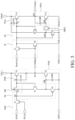
- FIG. 5 is a circuit diagram illustrating a gate driving circuit of the electroluminescent display device 100 according to an embodiment of the present disclosure.
- the electroluminescent display device 100 may include the gate driving circuit GD composed of separate gate signal generating circuits that swing the initialization signal.
- the widths of the gate driving circuit GD may increase due to additional circuits, but to prevent this, the emission signal generating circuit may be used.
- the emission signal generating circuit EDC(n) that provides the emission signal EM(n) and the initialization signal generating circuit VDC(n) that provides the initialization signal Vini(n) using the emission signal generating circuit EDC(n) will be described below.
- the emission signal generating circuit EDC(n) includes a first pull-down unit PDE, a first pull-up unit PUE, a Q node maintenance unit QS, a Q 2 node controller Q 2 C, and a Q node inverter QI.
- the first pull-down unit PDE outputs the emission signal EM(n) as a turn-on voltage in response to a voltage of a Q node
- the first pull-up unit PUE outputs the emission signal EM(n) as a turn-off voltage in response to a voltage of the QB node.
- the emission signal EM(n) determined by the first pull-down unit PDE and the first pull-up unit PUE is applied to the n-th pixel line PG(n).
- the Q node maintenance unit QS is connected between the Q node and a Q 2 node and serves as a buffer preventing a sudden change in voltage applied to the Q node.
- the Q node maintenance unit QS continuously electrically connects the Q node and the Q 2 node. Accordingly, a voltage of the Q 2 node maintains the same state as the voltage of the Q node.
- the Q 2 node controller Q 2 C is a component for charging or discharging the Q 2 node, and applies a turn-on voltage or a turn-off voltage to the Q 2 node using a start signal EVST.
- n is a natural number greater than or equal to 2
- the Q 2 node controller Q 2 C may use an output signal EM(n ⁇ 1) of an (n ⁇ 1)-th emission signal generating circuit EDC(n ⁇ 1) as a start signal.
- the Q node inverter QI applies a reversal voltage of the Q node to the QB node according to a Q 2 node voltage that is applied by the Q 2 node controller Q 2 C.
- the reversal voltage of the Q node is a voltage having a phase opposite to that of the voltage of the Q node.
- the initialization signal generating circuit VDC(n) includes a second pull-up unit PUV, a second pull-down unit PDV, a QB′ node maintenance unit QB′S, an emission signal inverter EI, and a Q′ node inverter Q′I.
- the second pull-up unit PUV outputs the initialization signal Vini(n) as a high level voltage in response to a voltage of the Q′ node
- the second pull-down unit PDV outputs the initialization signal Vini(n) as a low level voltage in response to a voltage of the QB′ node.
- the initialization signal Vini(n) determined by the second pull-up unit PUV and the second pull-down unit PDV is applied to the n-th pixel line PG(n).
- the QB′ node maintenance unit QB′S is connected between a QB′ node and a QB′ 2 node and serves as a buffer preventing a sudden change in voltage applied to the QB′ node.
- the QB′ node maintenance unit QB′S continuously electrically connects the QB′ node and the QB′ 2 node. Accordingly, a voltage of the QB′ 2 node maintains the same state as the voltage of the QB′ node.
- the emission signal inverter EI applies the first scan signal Scan 1 ( n ) or a voltage having a phase opposite to that of the emission signal EM(n) to the Q′ node according to the emission signal EM(n) output from the emission signal generating circuit EDC(n).
- the Q′ node inverter Q′I applies a reversal voltage of the Q′ node to the QB′ 2 node according to the voltage of the Q′ node that is applied by the emission signal inverter EI.
- the reversal voltage of the Q′ node is a voltage having a phase opposite to that of the voltage of the Q′ node.
- the turn-off voltage varies depending on a type of the transistor to which the turn-off voltage is applied.
- the turn-off voltage is at a high level for a p-type transistor and is at a low level for an n-type transistor.
- the turn-on voltage is at a low level for a p-type transistor and is at a high level for an n-type transistor.
- the gate signal generating circuit includes both an n-type transistor and a p-type transistor.
- the emission signal EM(n) and the initialization signal Vini(n) which are output signals of the gate signal generating circuit, are provided to the pixel circuit included in the n-th pixel line PG(n). A specific circuit structure and operation of the gate signal generating circuit will be described below.
- FIG. 6 is a waveform diagram of signals provided to the gate driving circuit of FIG. 5 .
- FIG. 7 A is a circuit diagram of the gate driving circuit according to an embodiment of the present disclosure during periods ⁇ circle around ( 1 ) ⁇ , ⁇ circle around ( 5 ) ⁇ , and ⁇ circle around ( 7 ) ⁇ of FIG. 6 .
- FIG. 7 B is a circuit diagram of the gate driving circuit according to an embodiment of the present disclosure during periods ⁇ circle around ( 2 ) ⁇ , ⁇ circle around ( 4 ) ⁇ , and ⁇ circle around ( 6 ) ⁇ of FIG. 6 .
- FIG. 7 C is a circuit diagram of the gate driving circuit according to an embodiment of the present disclosure during period ⁇ circle around ( 3 ) ⁇ of FIG. 6 .
- the gate driving circuit specifically means the gate signal generating circuit.
- the electroluminescent display device 100 may be driven dividedly in a refresh frame and an anode reset frame.
- the refresh frame may be divided into periods of ⁇ circle around ( 1 ) ⁇ , ⁇ circle around ( 2 ) ⁇ , ⁇ circle around ( 3 ) ⁇ , ⁇ circle around ( 4 ) ⁇ , and ⁇ circle around ( 5 ) ⁇
- the anode reset frame may be divided into periods of ⁇ circle around ( 5 ) ⁇ , ⁇ circle around ( 6 ) ⁇ , and ⁇ circle around ( 7 ) ⁇ .
- FIGS. 5 , 6 , and 7 A show the driving of the emission signal generating circuit EDC(n) and the initialization signal generating circuit VDC(n) during the periods ⁇ circle around ( 1 ) ⁇ , ⁇ circle around ( 5 ) ⁇ , and ⁇ circle around ( 7 ) ⁇ where the emission element EL emits light.
- the emission signal generating circuit EDC(n) outputs the emission signal EM(n) at a low level
- the initialization signal generating circuit VDC(n) also outputs the initialization signal Vini(n) at a low level.
- the Q 2 node controller Q 2 C provides a low level voltage to the Q 2 node.
- the Q 2 node controller Q 2 C is controlled by a clock signal ECLK and provides the start signal EVST or an emission signal EM(n ⁇ 1) of a previous row to the Q 2 node.
- the Q 2 node controller Q 2 C may be implemented as a first transistor T 1 .
- the first transistor T 1 may be a p-type MOSFET (PMOS) and may be implemented as a low-temperature polycrystalline silicon (LTPS) thin film transistor.
- PMOS p-type MOSFET
- LTPS low-temperature polycrystalline silicon
- the Q 2 node controller Q 2 C is turned on and transmits the low level to the Q 2 node. And, even when the clock signal ECLK is switched to a high level, the Q 2 node maintains the low level.
- the Q node maintenance unit QS electrically connects the Q node and the Q 2 node.
- the Q node maintenance unit QS is controlled by a first low voltage VGL 1 and electrically connects the Q node and the Q 2 node.
- the Q node maintenance unit QS may be implemented as a second transistor T 2 .
- the second transistor T 2 may be a p-type MOSFET (PMOS) and may be implemented as a low-temperature polycrystalline silicon (LTPS) thin film transistor. Since the first low voltage VGL 1 is applied to a gate electrode of the second transistor T 2 , the second transistor T 2 maintains a turned-on state all the time and electrically connects the Q node and the Q 2 node.
- PMOS p-type MOSFET
- LTPS low-temperature polycrystalline silicon
- the first pull-down unit PDE applies the first low voltage VGL 1 to a first output node EV.
- the first pull-down unit PDE is controlled by the Q node and provides the first low voltage VGL 1 to the first output node EV.
- the first pull-down unit PDE may be implemented as a fifth transistor T 5 and a Q node capacitor CQ.
- the fifth transistor T 5 may be a p-type MOSFET (PMOS) and may be implemented as a low-temperature polycrystalline silicon (LTPS) thin film transistor.
- the Q node capacitor CQ is connected to a gate electrode and a drain electrode of the fifth transistor T 5 .
- the Q node capacitor CQ rapidly applies the first low voltage VGL 1 to the first output node EV through a bootstrapping effect. Since the first output node EV is connected to a line to which the emission signal EM(n) is provided, the emission signal EM(n) is the first low voltage VGL 1 in the periods ⁇ circle around ( 1 ) ⁇ , ⁇ circle around ( 5 ) ⁇ , and ⁇ circle around ( 7 ) ⁇ .
- the Q node inverter QI provides a reversal voltage of the Q node to the QB node, so that the QB node becomes in a high level state.
- the Q node inverter QI includes a third transistor T 3 and a fourth transistor T 4 .
- the third transistor T 3 may be an n-type MOSFET (NMOS) and may be implemented as an oxide thin film transistor
- the fourth transistor T 4 may be a p-type MOSFET (PMOS) and may be implemented as a low-temperature polycrystalline silicon (LTPS) thin film transistor.
- NMOS n-type MOSFET
- PMOS p-type MOSFET
- LTPS low-temperature polycrystalline silicon
- the third transistor T 3 is turned off by the low level of the Q node, and the fourth transistor T 4 is turned on by the low level of the Q 2 node.
- the turned-on fourth transistor T 4 applies a first high voltage VGH 1 to the QB node. That is, in the periods ⁇ circle around ( 1 ) ⁇ , ⁇ circle around ( 5 ) ⁇ , and ⁇ circle around ( 7 ) ⁇ , the Q node is at a low level and the QB node is at a high level by the Q node inverter QI.
- the first pull-up unit PUE is controlled by the QB node and blocks the first high voltage VGH 1 to the first output node EV.
- the first pull-up unit PUE may be implemented as a sixth transistor T 6 and a QB node capacitor CQB.
- the sixth transistor T 6 may be a p-type MOSFET (PMOS) and may be implemented as a low-temperature polycrystalline silicon (LTPS) thin film transistor.
- the QB node capacitor CQB is connected to a gate electrode and a source electrode of the sixth transistor T 6 .
- the first pull-up unit PUE is turned off by the first high voltage VGH 1 of the QB node and does not apply the first high voltage VGH 1 to the first output node EV.
- the emission signal inverter EI is controlled by the emission signal EM(n) and provides a voltage having a phase opposite to that of the emission signal EM(n) to the Q′ node.
- the emission signal inverter EI may be implemented as a seventh transistor T 7 and an eighth transistor T 8 .
- the seventh transistor T 7 may be an n-type MOSFET (NMOS) and may be implemented as an oxide thin film transistor, and the eighth transistor T 8 may be a p-type MOSFET (PMOS) and may be implemented as a low-temperature polycrystalline silicon (LTPS) thin film transistor.
- the seventh transistor T 7 is controlled by the emission signal EM(n) and provides the first scan signal Scan 1 ( n ) to the Q′ node, and the eighth transistor T 8 is controlled by the emission signal EM(n) and provides the first high voltage VGH 1 to the Q′ node.
- the emission signal EM(n) is the first low voltage VGL 1 and the first scan signal Scan 1 ( n ) is at a low level, so that the seventh transistor T 7 is turned off and the eighth transistor T 8 is turned on. Accordingly, the emission signal inverter EI provides the first high voltage VGH 1 having a phase opposite to that of the emission signal EM(n) of the first low voltage VGL 1 to the Q′ node.
- the second pull-up unit PUV is controlled by the Q′ node and blocks a second high voltage VGH 2 to a second output node DV.
- the second pull-up unit PUV may be implemented as a twelfth transistor T 12 and a Q′ node capacitor CQ′.
- the twelfth transistor T 12 may be a p-type MOSFET (PMOS) and may be implemented as a low-temperature polycrystalline silicon (LTPS) thin film transistor.
- the Q′ node capacitor CQ′ is connected to a gate electrode and a source electrode of the twelfth transistor T 12 .
- the second pull-up unit PUV is turned off by the first high voltage VGH 1 of the Q′ node and does not apply the second high voltage VGH 2 to the second output node DV.
- the Q′ node inverter Q′I includes a ninth transistor T 9 and a tenth transistor T 10 .
- the ninth transistor T 9 may be a p-type MOSFET (PMOS) and may be implemented as a low-temperature polycrystalline silicon (LTPS) thin film transistor, and the tenth transistor T 10 may be an n-type MOSFET (NMOS) and may be implemented as an oxide thin film transistor.
- the ninth transistor T 9 is turned off by the first high voltage VGH 1 of the Q′ node, and the tenth transistor T 10 is turned on by the first high voltage VGH 1 of the Q′ node.
- the turned-on tenth transistor T 10 applies the first low voltage VGL 1 to the QB ‘ 2 node.
- the Q’ node is at the high level (or is the first high voltage VGH 1 ), and the QB′ 2 node is at the low level (or is the first low voltage VGL 1 ) by the Q′ node inverter Q′I.
- the QB′ node maintenance unit QB′S electrically connects the QB′ node and the QB′ 2 node.
- the QB′ node maintenance unit QB′S is controlled by the first low voltage VGL 1 and electrically connects the QB′ node and the QB′ 2 node.
- the QB′ node maintenance unit QB′S may be implemented as an eleventh transistor T 11 .
- the eleventh transistor T 11 may be a p-type MOSFET (PMOS) and may be implemented as a low-temperature polycrystalline silicon (LTPS) thin film transistor.
- PMOS p-type MOSFET
- LTPS low-temperature polycrystalline silicon
- the eleventh transistor T 11 Since the first low voltage VGL 1 is provided to a gate electrode of the eleventh transistor T 11 , the eleventh transistor T 11 maintains a turned-on state all the time and electrically connects the QB′ node and the QB′ 2 node. Since the QB′ 2 node is in a state of the first low voltage VGL 1 by the Q′ node inverter Q′I in the periods ⁇ circle around ( 1 ) ⁇ , ⁇ circle around ( 5 ) ⁇ , and ⁇ circle around ( 7 ) ⁇ , the QB′ node also becomes the first low voltage VGL 1 by the QB′ node maintenance unit QB′S.
- the second pull-down unit PDV applies a second low voltage VGL 2 to the second output node DV.
- the second pull-down unit PDV is controlled by the QB′ node and provides the second low voltage VGL 2 to the second output node DV.
- the second pull-down unit PDV may be implemented as a thirteenth transistor T 13 and a QB′ node capacitor CQB′.
- the thirteenth transistor T 13 may be a p-type MOSFET (PMOS) and may be implemented as a low-temperature polycrystalline silicon (LTPS) thin film transistor.
- PMOS p-type MOSFET
- LTPS low-temperature polycrystalline silicon
- the QB′ node capacitor CQB′ is connected to a gate electrode and a drain electrode of the thirteenth transistor T 13 .
- the QB′ node capacitor CQB′ rapidly applies the second low voltage VGL 2 to the second output node DV through a bootstrapping effect. Since the second output node DV is connected to a line to which the initialization signal Vini(n) is provided, the initialization signal Vini(n) is the second low voltage VGL 2 in the periods ⁇ circle around ( 1 ) ⁇ , ⁇ circle around ( 5 ) ⁇ , and ⁇ circle around ( 7 ) ⁇ .
- the first low voltage VGL 1 and the first high voltage VGH 1 are respectively used as driving voltages for driving the gate driving circuit and may be referred to as a low level and a high level.
- the second low voltage VGL 2 and the second high voltage VGH 2 are voltages different from the first low voltage VGL 1 and the first high voltage VGH 1 , respectively, and are used as voltages for implementing the initialization signal Vini(n).
- the second high voltage VGH 2 is lower than the first high voltage VGH 1 and is a voltage at a level similar to that of a black voltage in order to have an effect on the on bias stress of the transistor.
- the second low voltage VGL 2 is higher than the first low voltage VGL 1 and is a voltage at a level similar to that of the low potential driving voltage VSS.
- FIGS. 5 , 6 , and 7 B in which driving of the emission signal generating circuit EDC(n) and the initialization signal generating circuit VDC(n) during the periods of ⁇ circle around ( 2 ) ⁇ , ⁇ circle around ( 4 ) ⁇ , and ⁇ circle around ( 6 ) ⁇ is shown.
- An on-bias voltage is applied to the driving transistor in the periods of ⁇ circle around ( 2 ) ⁇ , ⁇ circle around ( 4 ) ⁇ , and ⁇ circle around ( 6 ) ⁇ .
- the emission signal generating circuit EDC(n) outputs the emission signal EM(n) of a high level
- the initialization signal generating circuit VDC(n) also outputs the initialization signal Vini(n) of a high level.
- the Q 2 node controller Q 2 C provides a high level voltage to the Q 2 node.
- the Q 2 node controller Q 2 C is controlled by the clock signal ECLK and provides the start signal EVST or the emission signal EM(n ⁇ 1) of the previous row to the Q 2 node. In this case, since the clock signal ECLK is at a low level and the start signal EVST is at a high level, the Q 2 node controller Q 2 C is turned on and transmits the high level to the Q 2 node.
- the Q node maintenance unit QS electrically connects the Q node and the Q 2 node.
- the first pull-down unit PDE is controlled by the Q node and blocks the first low voltage VGL 1 .
- the first pull-down unit PDE is turned off by the high level voltage of the Q node and does not apply the first low voltage VGL 1 to the first output node EV.
- the Q node inverter QI since the Q node inverter QI provides a reversal voltage of the Q node to the QB node, the QB node becomes in a low level state.
- the third transistor T 3 constituting the Q node inverter QI is turned on by the high level of the Q node, and the fourth transistor T 4 is turned off by the high level of the Q 2 node.
- the turned-on third transistor T 3 applies the first low voltage VGL 1 to the QB node.
- the Q node is at a high level, and the QB node becomes at a low level by the Q node inverter QI.
- the first pull-up unit PUE is controlled by the QB node and transmits the first high voltage VGH 1 to the first output node EV.
- the sixth transistor T 6 constituting the first pull-up unit PUE is turned on by the first low voltage VGL 1 of the QB node and applies the first high voltage VGH 1 to the first output node EV.
- the QB node capacitor CQB rapidly applies the first high voltage VGH 1 to the first output node EV through a bootstrapping effect and maintains a voltage of the QB node to the first low voltage VGL 1 .
- the emission signal EM(n) is the first high voltage VGH 1 in the periods ⁇ circle around ( 2 ) ⁇ , ⁇ circle around ( 4 ) ⁇ , and ⁇ circle around ( 6 ) ⁇ .
- the emission signal inverter EI is controlled by the emission signal EM(n) and provides the first scan signal Scan( 1 ) to the Q′ node.
- the seventh transistor T 7 constituting the emission signal inverter EI is turned on by the first high voltage VGH 1 of the emission signal EM(n) and provides the first scan signal Scan 1 ( n ) to the Q′ node, and the eighth transistor T 8 is turned off by the first high voltage VGH 1 of the emission signal EM(n).
- the emission signal inverter EI provides the first scan signal Scan( 1 ) of the low level voltage to the Q′ node.
- the second pull-up unit PUV is controlled by the Q′ node and transmits the second high voltage VGH 2 to the second output node DV.
- the twelfth transistor T 12 constituting the second pull-up unit PUV is turned on by the low level voltage of the Q′ node and applies the second high voltage VGH 2 to the second output node DV.
- the Q′ node capacitor CQ′ may rapidly apply the second high voltage VGH 2 to the second output node DV through a bootstrapping effect and may maintain the voltage of the Q′ node to the low level voltage.
- the initialization signal Vini(n) is the second high voltage VGH 2 in the periods ⁇ circle around ( 2 ) ⁇ , ⁇ circle around ( 4 ) ⁇ , and ⁇ circle around ( 6 ) ⁇ .
- the Q′ node inverter Q′I provides a reversal voltage of the Q′ node to the QB′ 2 node
- the QB′ 2 node becomes in a high level state.
- the ninth transistor T 9 constituting the Q′ node inverter Q′I is turned on by the low level voltage of the Q′ node and applies the second high voltage VGH 2 to the QB ‘ 2 node, and the tenth transistor T 10 is turned off by the low level voltage of the Q’ node.
- the Q′ node is at a low level, and the QB ‘ 2 node becomes the second high voltage VGH 2 by the Q’ node inverter Q′I.
- the QB′ node maintenance unit QB′S electrically connects the QB′ node and the QB′ 2 node. Since the QB′ 2 node is in a state of the second high voltage VGH 2 by the Q′ node inverter Q′I, the QB′ node also becomes the second high voltage VGH 2 by the QB′ node maintenance unit QB′S.
- the second pull-down unit PDV blocks the second low voltage VGL 2 .
- the thirteenth transistor T 13 constituting the second pull-down unit PDV is turned off by the second high voltage VGH 2 of the QB′ node and does not apply the second low voltage VGL 2 to the second output node DV.
- FIGS. 5 , 6 , and 7 C show driving of the emission signal generating circuit EDC(n) and the initialization signal generating circuit VDC(n) during period ⁇ circle around ( 3 ) ⁇ where the gate electrode and the drain electrode of the driving transistor are initialized.
- the emission signal generating circuit EDC(n) outputs the emission signal EM(n) of a high level
- the initialization signal generating circuit VDC(n) outputs the initialization signal Vini(n) of a low level.
- the Q 2 node controller Q 2 C maintains the high level voltage applied to the Q 2 node in the period ⁇ circle around ( 2 ) ⁇ . And, since the Q node maintenance unit QS electrically connects the Q node and the Q 2 node, the Q 2 node is also at a high level.
- the first pull-down unit PDE is blocked by the high level voltage of the Q node and does not apply the first low voltage VGL 1 to the first output node EV.
- the Q node inverter QI provides a reversal voltage of the Q node to the QB node, the QB node becomes in a low level state.
- the third transistor T 3 constituting the Q node inverter QI is turned on by the high level of the Q node, and the fourth transistor T 4 is turned off by the high level of the Q 2 node.
- the turned-on third transistor T 3 applies the first low voltage VGL 1 to the QB node. That is, in the period ⁇ circle around ( 3 ) ⁇ , the Q node is at a high level, and the QB node becomes at a low level by the Q node inverter QI.
- the first pull-up unit PUE is controlled by the QB node and transmits the first high voltage VGH 1 to the first output node EV.
- the sixth transistor T 6 constituting the first pull-up unit PUE is turned on by the first low voltage VGL 1 of the QB node and applies the first high voltage VGH 1 to the first output node EV.
- the QB node capacitor CQB maintains the QB node to the first low voltage VGL 1 and continuously applies the first high voltage VGH 1 to the first output node EV. Since the first output node EV is connected to the line to which the emission signal EM(n) is provided, the emission signal EM(n) is the first high voltage VGH 1 in the period ⁇ circle around ( 3 ) ⁇ .
- the emission signal inverter EI is controlled by the emission signal EM(n) and provides the first scan signal Scan( 1 ) to the Q′ node.
- the seventh transistor T 7 constituting the emission signal inverter EI is turned on by the first high voltage VGH 1 of the emission signal EM(n) and provides the first scan signal Scan 1 ( n ) to the Q′ node, and the eighth transistor T 8 is turned off by the first high voltage VGH 1 of the emission signal EM(n).
- the emission signal inverter EI provides the first scan signal Scan 1 ( n ) of the high level to the Q′ node.
- the second pull-up unit PUV is controlled by the Q′ node and blocks the second high voltage VGH 2 to the second output node DV.
- the twelfth transistor T 12 constituting the second pull-up unit PUV is turned off by the high level voltage of the Q′ node and does not apply the second high voltage VGH 2 to the second output node DV.
- the Q′ node inverter Q′I provides a reversal voltage of the Q′ node to the QB′ 2 node
- the QB′ 2 node becomes in a low level state.
- the ninth transistor T 9 constituting the Q′ node inverter Q′I is turned off by the high level voltage of the Q′ node, and the tenth transistor T 10 is turned on by the high level voltage of the Q′ node.
- the turned-on tenth transistor T 10 applies the first low voltage VGL 1 to the QB′ 2 node. That is, in the period ⁇ circle around ( 3 ) ⁇ , the Q′ node is at a high level, and the QB′ 2 node becomes the first low voltage VGL 1 by the Q′ node inverter Q′I.
- the QB′ node maintenance unit QB′S electrically connects the QB′ node and the QB′ 2 node. Since the QB′ 2 node is in a state of the first low voltage VGL 1 by the Q′ node inverter Q′I in the period ⁇ circle around ( 3 ) ⁇ , the QB′ node also becomes the first low voltage VGL 1 by the QB′ node maintenance unit QB′S.
- the second pull-down unit PDV applies the second low voltage VGL 2 to the second output node DV.
- the second pull-down unit PDV is controlled by the QB′ node and provides the second low voltage VGL 2 to the second output node DV.
- the thirteenth transistor T 13 constituting the second pull-down unit PDV is turned on and provides the second low voltage VGL 2 to the second output node DV.
- the QB′ node capacitor CQB′ rapidly applies the second low voltage VGL 2 to the second output node DV through a bootstrapping effect, and maintains the voltage of the QB′ node to the first low voltage VGL 1 . Since the second output node DV is connected to the line to which the initialization signal Vini(n) is provided, the initialization signal Vini(n) is the second low voltage VGL 2 in the period ⁇ circle around ( 3 ) ⁇ .
- an electroluminescent display device includes a pixel circuit implemented with a plurality of transistors, and a gate driving circuit that provides a scan signal, an initialization signal, and an emission signal to the pixel circuit.
- the gate driving circuit includes a scan signal generating circuit that provides the scan signal to a gate electrode of at least one of the plurality of transistors, an initialization signal generating circuit that provides the initialization signal to a source electrode or a drain electrode of at least one of the plurality of transistors, and an emission signal generating circuit that provides the emission signal to the gate electrode of at least one of the plurality of transistors.
- the initialization signal generating circuit receives an output signal of the scan signal generating circuit and an output signal of the emission signal generating circuit.
- the initialization signal generating circuit and the emission signal generating circuit include an n-type transistor and a p-type transistor.
- the emission signal generating circuit may include a first pull-down unit controlled by a Q node and a first pull-up unit controlled by a QB node, the QB node may be coupled to a Q node inverter that provides a reversal voltage of the Q node to the QB node.
- the initialization signal generating circuit may include a second pull-up unit controlled by a Q′ node and a second pull-down unit controlled by a QB′ node, the QB′ node is coupled to a Q′ node inverter that provides a reversal voltage of the Q′ node to the QB′ node, the Q′ node inverter is coupled to an emission signal inverter that provides the output signal of the scan signal generating circuit or a voltage having a phase opposite to that of the output signal of the emission signal generating circuit to the Q′ node.
- the plurality of transistors may include at least one n-type transistor and at least one p-type transistor.
- the scan signal generating circuit may be coupled to a gate electrode of the at least one n-type transistor.
- the emission signal generating circuit may be coupled to a gate electrode of the at least one p-type transistor.
- the initialization signal generating circuit may be connected to a source electrode or a drain electrode of another p-type transistor other than the p-type transistor coupled to the emission signal generating circuit.
- the initialization signal may be a signal swinging between a high level and a low level within one frame.
- the electroluminescent display device may further include a plurality of pixel lines each including a plurality of pixel circuits.
- the gate driving circuit may include a first gate driving circuit and a second gate driving circuit.
- the first gate driving circuit may include a first scan signal generating circuit that provides a scan signal for sampling a threshold voltage of a driving transistor, a second scan signal generating circuit that provides for controlling a data voltage to be applied to the pixel circuit, and a third scan signal generating circuit that provides a scan signal for controlling the initialization signal to be provided to the pixel circuit.
- the second gate driving circuit may include the emission signal generating circuit, the second scan signal generating circuit, and the initialization signal generating circuit.
- the first gate driving circuit and the second gate driving circuit may share the second scan signal generating circuit coupled to an odd-numbered pixel circuit included in one pixel line and the second scan signal generating circuit coupled to an even-numbered pixel circuit in the one pixel line.
- the gate driving circuit includes a first pull-down unit controlled by a Q node, a first pull-up unit controlled by a QB node, a second pull-up unit controlled by a Q′ node, a second pull-down unit controlled by a QB′ node, a Q node inverter electrically connected to the Q node and the QB node to provide a reversal voltage of the Q node to the QB node, a Q′ node inverter electrically connected to the Q′ node and the QB′ node to provide a reversal voltage of the Q′ node to the QB′ node, and an emission signal inverter electrically connected to the Q′ node to provide a scan signal or a voltage having a phase opposite to that of an emission signal to the Q′ node.
- the first pull-down unit and the first pull-up unit output the emission signal.
- the second pull-up unit and the second pull-down unit output an emission signal inverter electrically connected to the Q′ no
- the first pull-down unit may be coupled to a line to which a first low voltage is provided.
- the first pull-up unit may be coupled to a line to which a first high voltage is provided.
- the second pull-up unit may be coupled to a line to which a second high voltage is provided.
- the second pull-down unit may be coupled to a line to which a second low voltage is provided.
- the gate driving circuit may further include a Q node maintenance unit electrically connecting the Q node inverter to the Q node.
- the Q node maintenance unit may be controlled by the first low voltage provided from the line coupled to the first pull-down unit and electrically connects the Q node and a Q 2 node.
- the Q node inverter may include an n-type transistor controlled by the Q node and a p-type transistor controlled by the Q 2 node.
- the gate driving circuit may further include a Q 2 node controller coupled to the Q 2 node, the Q 2 node controller may be controlled by a clock signal and may provide a start signal or an emission signal output from a previous row to the Q 2 node.
- the gate driving circuit may further include a QB′ node maintenance unit electrically connecting the Q′ node inverter to the QB′ node.
- the Q′ node inverter may be controlled by the Q′ node and may include an n-type transistor and a p-type transistor that are coupled at the QB′ 2 node.
- the n-type transistor may be coupled to a line to which the first low voltage is provided, and the p-type transistor may be coupled to a line to which the second high voltage is provided.
- the QB′ node maintenance unit may be controlled by the first low voltage provided from the line coupled to the n-type transistor and may electrically connect the QB′ node and the QB′ 2 node.
- the gate driving circuit may further include a scan signal generating circuit for outputting the scan signal.
- the emission signal inverter may include a p-type transistor and an n-type transistor controlled by the emission signal.
- Each of the first pull-down unit, the first pull-up unit, the second pull-up unit, and the second pull-down unit may include a p-type transistor and a capacitor coupling a gate electrode of the p-type transistor, and a drain electrode or a source electrode of the p-type transistor.
- the second high voltage may be lower than the first high voltage.
- the second low voltage may be higher than the first low voltage.
Landscapes
- Engineering & Computer Science (AREA)
- Physics & Mathematics (AREA)
- Computer Hardware Design (AREA)
- General Physics & Mathematics (AREA)
- Theoretical Computer Science (AREA)
- Control Of Indicators Other Than Cathode Ray Tubes (AREA)
- Electroluminescent Light Sources (AREA)
Abstract
Description
Ioled=k/2(Vgs+|Vth|)2 =k/2(Vdata−VDD)2
Claims (9)
Priority Applications (1)
| Application Number | Priority Date | Filing Date | Title |
|---|---|---|---|
| US18/309,699 US12205519B2 (en) | 2020-12-23 | 2023-04-28 | Gate driving circuit and electroluminescent display device using the same |
Applications Claiming Priority (4)
| Application Number | Priority Date | Filing Date | Title |
|---|---|---|---|
| KR1020200181933A KR20220090924A (en) | 2020-12-23 | 2020-12-23 | Gate driving circuit and electroluminescence display device using the same |
| KR10-2020-0181933 | 2020-12-23 | ||
| US17/555,799 US11676528B2 (en) | 2020-12-23 | 2021-12-20 | Gate driving circuit and electroluminescent display device using the same |
| US18/309,699 US12205519B2 (en) | 2020-12-23 | 2023-04-28 | Gate driving circuit and electroluminescent display device using the same |
Related Parent Applications (1)
| Application Number | Title | Priority Date | Filing Date |
|---|---|---|---|
| US17/555,799 Continuation US11676528B2 (en) | 2020-12-23 | 2021-12-20 | Gate driving circuit and electroluminescent display device using the same |
Publications (2)
| Publication Number | Publication Date |
|---|---|
| US20230267872A1 US20230267872A1 (en) | 2023-08-24 |
| US12205519B2 true US12205519B2 (en) | 2025-01-21 |
Family
ID=81847115
Family Applications (2)
| Application Number | Title | Priority Date | Filing Date |
|---|---|---|---|
| US17/555,799 Active US11676528B2 (en) | 2020-12-23 | 2021-12-20 | Gate driving circuit and electroluminescent display device using the same |
| US18/309,699 Active US12205519B2 (en) | 2020-12-23 | 2023-04-28 | Gate driving circuit and electroluminescent display device using the same |
Family Applications Before (1)
| Application Number | Title | Priority Date | Filing Date |
|---|---|---|---|
| US17/555,799 Active US11676528B2 (en) | 2020-12-23 | 2021-12-20 | Gate driving circuit and electroluminescent display device using the same |
Country Status (4)
| Country | Link |
|---|---|
| US (2) | US11676528B2 (en) |
| KR (1) | KR20220090924A (en) |
| CN (1) | CN114664214B (en) |
| DE (1) | DE102021133244A1 (en) |
Families Citing this family (9)
| Publication number | Priority date | Publication date | Assignee | Title |
|---|---|---|---|---|
| US12175930B2 (en) * | 2020-10-15 | 2024-12-24 | Xiamen Tianma Micro-Electronics Co., Ltd. | Display panel |
| KR20230143650A (en) * | 2022-04-05 | 2023-10-13 | 삼성디스플레이 주식회사 | Pixel circuit and display apparatus having the same |
| US11557253B2 (en) * | 2022-05-10 | 2023-01-17 | Google Llc | Image retention mitigation via voltage biasing for organic lighting-emitting diode displays |
| KR20240033509A (en) * | 2022-09-05 | 2024-03-12 | 엘지디스플레이 주식회사 | Pixel, Driving method for the Pixel and Display including the Pixel |
| CN117912395A (en) * | 2022-10-11 | 2024-04-19 | 荣耀终端有限公司 | Display panel, display driving method, display device and electronic equipment |
| KR20240100748A (en) | 2022-12-23 | 2024-07-02 | 엘지디스플레이 주식회사 | Display Device Including Stage Transistor |
| KR20240108906A (en) | 2022-12-30 | 2024-07-10 | 엘지디스플레이 주식회사 | Display apparatus and method for driving the same |
| CN116312386A (en) * | 2023-03-31 | 2023-06-23 | 昆山国显光电有限公司 | Display panel and display device |
| CN119851617A (en) * | 2025-02-28 | 2025-04-18 | 惠科股份有限公司 | Organic light emitting diode driving circuit, display panel and display device |
Citations (7)
| Publication number | Priority date | Publication date | Assignee | Title |
|---|---|---|---|---|
| KR20150059604A (en) | 2013-11-21 | 2015-06-01 | 엘지디스플레이 주식회사 | Organic Light Emitting Diode Display |
| US20160035277A1 (en) | 2014-07-29 | 2016-02-04 | Lg Display Co., Ltd. | Organic light emitting display device and method of driving the same |
| US20170116925A1 (en) * | 2015-10-23 | 2017-04-27 | Lg Display Co., Ltd. | Scan driver, display device, and method of driving display device |
| KR20180004369A (en) | 2016-07-01 | 2018-01-11 | 삼성디스플레이 주식회사 | Pixel and stage circuit and organic light emitting display device having the pixel and the stage circuit |
| US20190066604A1 (en) | 2017-08-31 | 2019-02-28 | Lg Display Co., Ltd. | Gate driving circuit and electroluminescent display using the same |
| US20190156732A1 (en) * | 2017-11-21 | 2019-05-23 | Lg Display Co., Ltd. | Gate driver and electroluminescence display device including the same |
| US20220069044A1 (en) | 2020-08-31 | 2022-03-03 | Samsung Display Co., Ltd. | Display device |
Family Cites Families (10)
| Publication number | Priority date | Publication date | Assignee | Title |
|---|---|---|---|---|
| KR100682361B1 (en) * | 2005-06-28 | 2007-02-15 | 엘지.필립스 엘시디 주식회사 | Organic light emitting diode display and its driving device |
| KR20140077552A (en) * | 2012-12-14 | 2014-06-24 | 삼성디스플레이 주식회사 | Organic Light Emitting Display Device and Driving Method Thereof |
| KR102048562B1 (en) * | 2013-05-13 | 2019-11-26 | 삼성디스플레이 주식회사 | Organic Light Emitting Display Device and Driving Method Threrof |
| CN104658475B (en) * | 2013-11-21 | 2017-04-26 | 乐金显示有限公司 | Organic light emitting diode display device |
| CN105702222B (en) * | 2016-04-18 | 2018-06-08 | 京东方科技集团股份有限公司 | Shift register cell, gate drive apparatus, display device and driving method |
| KR102523646B1 (en) * | 2017-11-01 | 2023-04-21 | 삼성디스플레이 주식회사 | Display device and driving method thereof |
| US10916198B2 (en) * | 2019-01-11 | 2021-02-09 | Apple Inc. | Electronic display with hybrid in-pixel and external compensation |
| CN110619852B (en) * | 2019-09-26 | 2020-11-13 | 昆山工研院新型平板显示技术中心有限公司 | Scanning circuit, display panel and display device |
| CN111445863B (en) * | 2020-05-14 | 2021-09-14 | 京东方科技集团股份有限公司 | Pixel driving circuit, driving method thereof and display device |
| CN111883042B (en) * | 2020-07-31 | 2023-06-23 | 维信诺科技股份有限公司 | Display panel and display device |
-
2020
- 2020-12-23 KR KR1020200181933A patent/KR20220090924A/en active Pending
-
2021
- 2021-12-08 CN CN202111493036.4A patent/CN114664214B/en active Active
- 2021-12-15 DE DE102021133244.3A patent/DE102021133244A1/en active Pending
- 2021-12-20 US US17/555,799 patent/US11676528B2/en active Active
-
2023
- 2023-04-28 US US18/309,699 patent/US12205519B2/en active Active
Patent Citations (9)
| Publication number | Priority date | Publication date | Assignee | Title |
|---|---|---|---|---|
| KR20150059604A (en) | 2013-11-21 | 2015-06-01 | 엘지디스플레이 주식회사 | Organic Light Emitting Diode Display |
| US20160035277A1 (en) | 2014-07-29 | 2016-02-04 | Lg Display Co., Ltd. | Organic light emitting display device and method of driving the same |
| CN105321472A (en) * | 2014-07-29 | 2016-02-10 | 乐金显示有限公司 | Organic light emitting display device and method of driving the same |
| US20170116925A1 (en) * | 2015-10-23 | 2017-04-27 | Lg Display Co., Ltd. | Scan driver, display device, and method of driving display device |
| KR20170047633A (en) | 2015-10-23 | 2017-05-08 | 엘지디스플레이 주식회사 | Scan Driver, Display Device and Driving Method of Display Device |
| KR20180004369A (en) | 2016-07-01 | 2018-01-11 | 삼성디스플레이 주식회사 | Pixel and stage circuit and organic light emitting display device having the pixel and the stage circuit |
| US20190066604A1 (en) | 2017-08-31 | 2019-02-28 | Lg Display Co., Ltd. | Gate driving circuit and electroluminescent display using the same |
| US20190156732A1 (en) * | 2017-11-21 | 2019-05-23 | Lg Display Co., Ltd. | Gate driver and electroluminescence display device including the same |
| US20220069044A1 (en) | 2020-08-31 | 2022-03-03 | Samsung Display Co., Ltd. | Display device |
Also Published As
| Publication number | Publication date |
|---|---|
| CN114664214A (en) | 2022-06-24 |
| US20220208074A1 (en) | 2022-06-30 |
| CN114664214B (en) | 2025-09-30 |
| DE102021133244A1 (en) | 2022-06-23 |
| US20230267872A1 (en) | 2023-08-24 |
| KR20220090924A (en) | 2022-06-30 |
| US11676528B2 (en) | 2023-06-13 |
Similar Documents
| Publication | Publication Date | Title |
|---|---|---|
| US11594169B2 (en) | Gate driving circuit and electroluminescent display device using the same | |
| US12205519B2 (en) | Gate driving circuit and electroluminescent display device using the same | |
| US10559261B2 (en) | Electroluminescent display | |
| US9159265B2 (en) | Pixel, display device including the same, and driving method thereof | |
| US11929024B2 (en) | Organic light emitting display device | |
| CN115064114A (en) | Light emitting display device | |
| US11972735B2 (en) | Display device | |
| US20250095594A1 (en) | Gate driving circuit and display device using the same | |
| US11869433B2 (en) | Pixel and display apparatus including the same | |
| US11568824B2 (en) | Electroluminescence display device | |
| US12277894B2 (en) | Gate driving circuit and electroluminescence display device using the same | |
| KR20240070087A (en) | Light emitting display device | |
| KR102431625B1 (en) | Organic light emitting display device and driving method of the same | |
| KR102616670B1 (en) | Display device | |
| US11475846B2 (en) | Display apparatus | |
| US20250218390A1 (en) | Gate driver and display device including the same | |
| US11475847B2 (en) | Display apparatus | |
| KR102710293B1 (en) | Electroluminescence display device | |
| KR20240099875A (en) | Display device and driving method thereof | |
| US20260073876A1 (en) | Gate driving circuit, and display panel and display device including the gate driving circuit | |
| US20260051297A1 (en) | Gate driver and display device including the same | |
| KR20240107768A (en) | Display device | |
| KR20170124062A (en) | Organic Light Emitting Display |
Legal Events
| Date | Code | Title | Description |
|---|---|---|---|
| FEPP | Fee payment procedure |
Free format text: ENTITY STATUS SET TO UNDISCOUNTED (ORIGINAL EVENT CODE: BIG.); ENTITY STATUS OF PATENT OWNER: LARGE ENTITY |
|
| STPP | Information on status: patent application and granting procedure in general |
Free format text: DOCKETED NEW CASE - READY FOR EXAMINATION |
|
| AS | Assignment |
Owner name: LG DISPLAY CO., LTD., KOREA, REPUBLIC OF Free format text: ASSIGNMENT OF ASSIGNORS INTEREST;ASSIGNORS:KIM, MINSU;KIM, SEHWAN;REEL/FRAME:063754/0626 Effective date: 20211206 |
|
| STPP | Information on status: patent application and granting procedure in general |
Free format text: NON FINAL ACTION COUNTED, NOT YET MAILED |
|
| STPP | Information on status: patent application and granting procedure in general |
Free format text: NON FINAL ACTION MAILED |
|
| STPP | Information on status: patent application and granting procedure in general |
Free format text: RESPONSE TO NON-FINAL OFFICE ACTION ENTERED AND FORWARDED TO EXAMINER |
|
| STPP | Information on status: patent application and granting procedure in general |
Free format text: NOTICE OF ALLOWANCE MAILED -- APPLICATION RECEIVED IN OFFICE OF PUBLICATIONS |
|
| ZAAB | Notice of allowance mailed |
Free format text: ORIGINAL CODE: MN/=. |
|
| STPP | Information on status: patent application and granting procedure in general |
Free format text: NOTICE OF ALLOWANCE MAILED -- APPLICATION RECEIVED IN OFFICE OF PUBLICATIONS |
|
| STPP | Information on status: patent application and granting procedure in general |
Free format text: PUBLICATIONS -- ISSUE FEE PAYMENT VERIFIED |
|
| STCF | Information on status: patent grant |
Free format text: PATENTED CASE |