US12200900B2 - Electronic device with heat-conductive cover - Google Patents
Electronic device with heat-conductive cover Download PDFInfo
- Publication number
- US12200900B2 US12200900B2 US17/386,540 US202117386540A US12200900B2 US 12200900 B2 US12200900 B2 US 12200900B2 US 202117386540 A US202117386540 A US 202117386540A US 12200900 B2 US12200900 B2 US 12200900B2
- Authority
- US
- United States
- Prior art keywords
- heat
- conducting
- package
- electronic device
- conducting cover
- Prior art date
- Legal status (The legal status is an assumption and is not a legal conclusion. Google has not performed a legal analysis and makes no representation as to the accuracy of the status listed.)
- Active, expires
Links
Images


Classifications
-
- H—ELECTRICITY
- H05—ELECTRIC TECHNIQUES NOT OTHERWISE PROVIDED FOR
- H05K—PRINTED CIRCUITS; CASINGS OR CONSTRUCTIONAL DETAILS OF ELECTRIC APPARATUS; MANUFACTURE OF ASSEMBLAGES OF ELECTRICAL COMPONENTS
- H05K7/00—Constructional details common to different types of electric apparatus
- H05K7/20—Modifications to facilitate cooling, ventilating, or heating
- H05K7/20218—Modifications to facilitate cooling, ventilating, or heating using a liquid coolant without phase change in electronic enclosures
-
- H—ELECTRICITY
- H05—ELECTRIC TECHNIQUES NOT OTHERWISE PROVIDED FOR
- H05K—PRINTED CIRCUITS; CASINGS OR CONSTRUCTIONAL DETAILS OF ELECTRIC APPARATUS; MANUFACTURE OF ASSEMBLAGES OF ELECTRICAL COMPONENTS
- H05K7/00—Constructional details common to different types of electric apparatus
- H05K7/20—Modifications to facilitate cooling, ventilating, or heating
- H05K7/20009—Modifications to facilitate cooling, ventilating, or heating using a gaseous coolant in electronic enclosures
- H05K7/20136—Forced ventilation, e.g. by fans
- H05K7/20172—Fan mounting or fan specifications
-
- G—PHYSICS
- G06—COMPUTING OR CALCULATING; COUNTING
- G06F—ELECTRIC DIGITAL DATA PROCESSING
- G06F1/00—Details not covered by groups G06F3/00 - G06F13/00 and G06F21/00
- G06F1/16—Constructional details or arrangements
- G06F1/20—Cooling means
-
- H01L25/0657—
-
- H—ELECTRICITY
- H05—ELECTRIC TECHNIQUES NOT OTHERWISE PROVIDED FOR
- H05K—PRINTED CIRCUITS; CASINGS OR CONSTRUCTIONAL DETAILS OF ELECTRIC APPARATUS; MANUFACTURE OF ASSEMBLAGES OF ELECTRICAL COMPONENTS
- H05K1/00—Printed circuits
- H05K1/02—Details
- H05K1/0201—Thermal arrangements, e.g. for cooling, heating or preventing overheating
- H05K1/0203—Cooling of mounted components
-
- H—ELECTRICITY
- H05—ELECTRIC TECHNIQUES NOT OTHERWISE PROVIDED FOR
- H05K—PRINTED CIRCUITS; CASINGS OR CONSTRUCTIONAL DETAILS OF ELECTRIC APPARATUS; MANUFACTURE OF ASSEMBLAGES OF ELECTRICAL COMPONENTS
- H05K7/00—Constructional details common to different types of electric apparatus
- H05K7/20—Modifications to facilitate cooling, ventilating, or heating
- H05K7/20009—Modifications to facilitate cooling, ventilating, or heating using a gaseous coolant in electronic enclosures
- H05K7/20136—Forced ventilation, e.g. by fans
- H05K7/20145—Means for directing air flow, e.g. ducts, deflectors, plenum or guides
-
- H—ELECTRICITY
- H05—ELECTRIC TECHNIQUES NOT OTHERWISE PROVIDED FOR
- H05K—PRINTED CIRCUITS; CASINGS OR CONSTRUCTIONAL DETAILS OF ELECTRIC APPARATUS; MANUFACTURE OF ASSEMBLAGES OF ELECTRICAL COMPONENTS
- H05K7/00—Constructional details common to different types of electric apparatus
- H05K7/20—Modifications to facilitate cooling, ventilating, or heating
- H05K7/20218—Modifications to facilitate cooling, ventilating, or heating using a liquid coolant without phase change in electronic enclosures
- H05K7/20236—Modifications to facilitate cooling, ventilating, or heating using a liquid coolant without phase change in electronic enclosures by immersion
-
- H—ELECTRICITY
- H05—ELECTRIC TECHNIQUES NOT OTHERWISE PROVIDED FOR
- H05K—PRINTED CIRCUITS; CASINGS OR CONSTRUCTIONAL DETAILS OF ELECTRIC APPARATUS; MANUFACTURE OF ASSEMBLAGES OF ELECTRICAL COMPONENTS
- H05K7/00—Constructional details common to different types of electric apparatus
- H05K7/20—Modifications to facilitate cooling, ventilating, or heating
- H05K7/20218—Modifications to facilitate cooling, ventilating, or heating using a liquid coolant without phase change in electronic enclosures
- H05K7/20254—Cold plates transferring heat from heat source to coolant
-
- H—ELECTRICITY
- H05—ELECTRIC TECHNIQUES NOT OTHERWISE PROVIDED FOR
- H05K—PRINTED CIRCUITS; CASINGS OR CONSTRUCTIONAL DETAILS OF ELECTRIC APPARATUS; MANUFACTURE OF ASSEMBLAGES OF ELECTRICAL COMPONENTS
- H05K7/00—Constructional details common to different types of electric apparatus
- H05K7/20—Modifications to facilitate cooling, ventilating, or heating
- H05K7/2029—Modifications to facilitate cooling, ventilating, or heating using a liquid coolant with phase change in electronic enclosures
- H05K7/20309—Evaporators
-
- H—ELECTRICITY
- H05—ELECTRIC TECHNIQUES NOT OTHERWISE PROVIDED FOR
- H05K—PRINTED CIRCUITS; CASINGS OR CONSTRUCTIONAL DETAILS OF ELECTRIC APPARATUS; MANUFACTURE OF ASSEMBLAGES OF ELECTRICAL COMPONENTS
- H05K7/00—Constructional details common to different types of electric apparatus
- H05K7/20—Modifications to facilitate cooling, ventilating, or heating
- H05K7/2039—Modifications to facilitate cooling, ventilating, or heating characterised by the heat transfer by conduction from the heat generating element to a dissipating body
- H05K7/205—Heat-dissipating body thermally connected to heat generating element via thermal paths through printed circuit board [PCB]
-
- H—ELECTRICITY
- H10—SEMICONDUCTOR DEVICES; ELECTRIC SOLID-STATE DEVICES NOT OTHERWISE PROVIDED FOR
- H10W—GENERIC PACKAGES, INTERCONNECTIONS, CONNECTORS OR OTHER CONSTRUCTIONAL DETAILS OF DEVICES COVERED BY CLASS H10
- H10W40/00—Arrangements for thermal protection or thermal control
- H10W40/20—Arrangements for cooling
- H10W40/22—Arrangements for cooling characterised by their shape, e.g. having conical or cylindrical projections
-
- H—ELECTRICITY
- H10—SEMICONDUCTOR DEVICES; ELECTRIC SOLID-STATE DEVICES NOT OTHERWISE PROVIDED FOR
- H10W—GENERIC PACKAGES, INTERCONNECTIONS, CONNECTORS OR OTHER CONSTRUCTIONAL DETAILS OF DEVICES COVERED BY CLASS H10
- H10W40/00—Arrangements for thermal protection or thermal control
- H10W40/40—Arrangements for thermal protection or thermal control involving heat exchange by flowing fluids
- H10W40/43—Arrangements for thermal protection or thermal control involving heat exchange by flowing fluids by flowing gases, e.g. forced air cooling
-
- H—ELECTRICITY
- H10—SEMICONDUCTOR DEVICES; ELECTRIC SOLID-STATE DEVICES NOT OTHERWISE PROVIDED FOR
- H10W—GENERIC PACKAGES, INTERCONNECTIONS, CONNECTORS OR OTHER CONSTRUCTIONAL DETAILS OF DEVICES COVERED BY CLASS H10
- H10W40/00—Arrangements for thermal protection or thermal control
- H10W40/40—Arrangements for thermal protection or thermal control involving heat exchange by flowing fluids
- H10W40/47—Arrangements for thermal protection or thermal control involving heat exchange by flowing fluids by flowing liquids, e.g. forced water cooling
-
- H—ELECTRICITY
- H10—SEMICONDUCTOR DEVICES; ELECTRIC SOLID-STATE DEVICES NOT OTHERWISE PROVIDED FOR
- H10W—GENERIC PACKAGES, INTERCONNECTIONS, CONNECTORS OR OTHER CONSTRUCTIONAL DETAILS OF DEVICES COVERED BY CLASS H10
- H10W90/00—Package configurations
-
- H01L23/427—
-
- H—ELECTRICITY
- H05—ELECTRIC TECHNIQUES NOT OTHERWISE PROVIDED FOR
- H05K—PRINTED CIRCUITS; CASINGS OR CONSTRUCTIONAL DETAILS OF ELECTRIC APPARATUS; MANUFACTURE OF ASSEMBLAGES OF ELECTRICAL COMPONENTS
- H05K1/00—Printed circuits
- H05K1/02—Details
- H05K1/0201—Thermal arrangements, e.g. for cooling, heating or preventing overheating
- H05K1/0203—Cooling of mounted components
- H05K1/0209—External configuration of printed circuit board adapted for heat dissipation, e.g. lay-out of conductors, coatings
-
- H—ELECTRICITY
- H05—ELECTRIC TECHNIQUES NOT OTHERWISE PROVIDED FOR
- H05K—PRINTED CIRCUITS; CASINGS OR CONSTRUCTIONAL DETAILS OF ELECTRIC APPARATUS; MANUFACTURE OF ASSEMBLAGES OF ELECTRICAL COMPONENTS
- H05K7/00—Constructional details common to different types of electric apparatus
- H05K7/20—Modifications to facilitate cooling, ventilating, or heating
- H05K7/20009—Modifications to facilitate cooling, ventilating, or heating using a gaseous coolant in electronic enclosures
- H05K7/20136—Forced ventilation, e.g. by fans
-
- H—ELECTRICITY
- H05—ELECTRIC TECHNIQUES NOT OTHERWISE PROVIDED FOR
- H05K—PRINTED CIRCUITS; CASINGS OR CONSTRUCTIONAL DETAILS OF ELECTRIC APPARATUS; MANUFACTURE OF ASSEMBLAGES OF ELECTRICAL COMPONENTS
- H05K7/00—Constructional details common to different types of electric apparatus
- H05K7/20—Modifications to facilitate cooling, ventilating, or heating
- H05K7/2029—Modifications to facilitate cooling, ventilating, or heating using a liquid coolant with phase change in electronic enclosures
- H05K7/20336—Heat pipes, e.g. wicks or capillary pumps
-
- H—ELECTRICITY
- H10—SEMICONDUCTOR DEVICES; ELECTRIC SOLID-STATE DEVICES NOT OTHERWISE PROVIDED FOR
- H10W—GENERIC PACKAGES, INTERCONNECTIONS, CONNECTORS OR OTHER CONSTRUCTIONAL DETAILS OF DEVICES COVERED BY CLASS H10
- H10W40/00—Arrangements for thermal protection or thermal control
- H10W40/70—Fillings or auxiliary members in containers or in encapsulations for thermal protection or control
- H10W40/73—Fillings or auxiliary members in containers or in encapsulations for thermal protection or control for cooling by change of state
-
- H—ELECTRICITY
- H10—SEMICONDUCTOR DEVICES; ELECTRIC SOLID-STATE DEVICES NOT OTHERWISE PROVIDED FOR
- H10W—GENERIC PACKAGES, INTERCONNECTIONS, CONNECTORS OR OTHER CONSTRUCTIONAL DETAILS OF DEVICES COVERED BY CLASS H10
- H10W90/00—Package configurations
- H10W90/20—Configurations of stacked chips
- H10W90/288—Configurations of stacked chips characterised by arrangements for thermal management of the stacked chips
Definitions
- This application relates to an electronic device, and particularly relates to an electronic device with a heat dissipation means.
- POP Package on package
- a memory chip may be disposed above the central processing unit.
- the central processing unit may generate a great amount of heat, and the memory chip located above the central processing unit may affect the heat dissipation efficiency of the central processing unit, thereby causing performance reduction of, or even damage to, the central processing unit.
- This application provides an electronic device in which an issue of poor heat dissipation efficiency of a package on package structure can be improved.
- the electronic device of this application includes a circuit board, a package on package structure, a heat-conducting cover, and a heat-conducting fluid.
- the circuit board has a first surface and a second surface opposite to each other.
- the package on package structure is disposed on the first surface.
- the package on package structure has at least one heat generating element.
- the heat-conducting cover is disposed on the second surface and is in thermal contact with the circuit board.
- the heat-conducting cover and the second surface form an enclosed space.
- the heat-conducting fluid is filled in the enclosed space.
- a heat dissipation means formed by the heat-conducting cover and the heat-conducting fluid is disposed on the back of the circuit board, which can improve the heat dissipation efficiency of the package on package structure.
- FIG. 1 is a schematic cross-sectional view of an electronic device according to an embodiment of the disclosure.
- FIG. 2 is a schematic cross-sectional view of an electronic device according to another embodiment of the disclosure.
- FIG. 3 is a schematic cross-sectional view of an electronic device according to still another embodiment of the disclosure.
- FIG. 1 is a schematic cross-sectional view of an electronic device according to an embodiment of the disclosure.
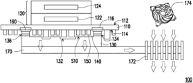
- an electronic device 100 of this embodiment includes a circuit board 110 , a package on package structure (POP structure) 120 , a heat-conducting cover 130 , and a heat-conducting fluid 140 .
- the circuit board 110 has a first surface 112 and a second surface 114 opposite to each other.
- the package on package structure 120 is disposed on the first surface 112 .
- the package on package structure 120 has at least one heat generating element 122 .
- the heat-conducting cover 130 is disposed on the second surface 114 and is in thermal contact with the circuit board 110 .
- the heat-conducting cover 130 and the second surface 114 form an enclosed space S 10 .
- the heat-conducting fluid 140 is filled in the enclosed space S 10 .
- the circuit board 110 , the heat-conducting cover 130 , and the heat-conducting fluid 140 form a heat dissipation means similar to a vapor chamber formed by two heat-conducting plates and a heat-conducting fluid therein.
- the electronic device 100 of this embodiment has a less overall thickness.
- the combination of the heat-conducting cover 130 and the heat-conducting fluid 140 also exhibits a good heat dissipation effect.
- the heat generating element 122 is a central processing unit, but may also be an image processing chip or other high-power chips.
- the package on package structure 120 may further have a chip 124 disposed on the heat generating element 122 .
- the chip 124 may be a memory chip or other types of chips.
- the chips 124 may include one chip or a plurality of chips, and the plurality of chips 124 may be arranged side by side or stacked on the heat generating element 122 .
- the electronic device 100 of this embodiment may further include a plurality of electronic components 150 disposed on the second surface 114 and located in the enclosed space S 10 .
- the electronic components 150 may be chips or passive elements, and the passive elements may be resistors, capacitors, or inductors.
- the conventional heat sink or vapor chamber may be affected by the electronic components 150 and thus cannot be used.
- the heat-conducting fluid 140 is filled between the electronic components 150 . Therefore, the size of the area available for the electronic components 150 to be disposed on the second surface 114 of the circuit board 110 is not greatly affected by the disposed heat-conducting cover 130 .
- the heat-conducting fluid 140 filled between the electronic components 150 may still quickly dissipate heat to prevent damage caused by a local high temperature.
- the heat-conducting fluid 140 has a high thermal conductivity coefficient and an electrical insulation property.
- the heat-conducting fluid 140 is not limited to water, and may also be other fluids having a high thermal conductivity coefficient, as long as it is likely to be reliably filled in the enclosed space S 10 .
- a thermal paste or a phase change material may also serve as the heat-conducting fluid 140 .
- the chip 124 is disposed on the heat generating element 122 , heat generated by the heat generating element 122 is not easily transferred to the external environment through the chip 124 .
- the heat-conducting cover 130 is disposed below the heat generating element 122 and filled with the heat-conducting fluid 140 , the heat generated by the heat generating element 122 is relatively easily transferred to the heat-conducting cover 130 and the heat-conducting fluid 140 through the internal circuits of the circuit board 110 .
- the electronic components 150 also facilitate heat dissipation and increase the contact area with the heat-conducting fluid 140 .
- the heat generating element 122 instantly increases power or calculation speed, the heat generating element 122 instantly generates more heat energy, that is, thermal impact.
- the heat-conducting fluid 140 and the heat-conducting cover 130 of this embodiment quickly absorb heat energy to reduce the influence by thermal impact.
- the heat generating element 122 instantly increases power or calculation speed, the local temperature does not rise overly high, and the influence on the service life of the package on package structure 120 is reduced.
- an inner surface 132 of the heat-conducting cover 130 located in the enclosed space S 10 and opposite to the second surface 114 is non-planar.
- a distance is kept between the inner surface 132 and the electronic components 150 . Therefore, a thermal resistance between the heat-conducting cover 130 and the electronic components 150 can be reduced, helping to increase the heat dissipation efficiency.
- the distance between the heat-conducting cover 130 and the electronic components 150 may affect the thermal resistance. As the distance decreases, the thermal resistance decreases, and the heat dissipation efficiency increases.
- the distance between the inner surface 132 and the electronic components 150 is preferred to be shortest possible without causing a short circuit.
- the heat-conducting cover 130 has an inlet 134 and an outlet 136 .
- the inlet 134 is used for the heat-conducting fluid 140 to be filled in the enclosed space S 10
- the outlet 136 is used for air and excess of the heat-conducting fluid 140 to flow out.
- the heat-conducting cover 130 is first bonded to the second surface 114 of the circuit board 110 , and then, the heat-conducting fluid 140 is filled from the inlet 134 into the enclosed space S 10 . During this process, air in the enclosed space S 10 may be discharged from the outlet 136 .
- the inlet 134 and the outlet 136 may be closed to enclose the heat-conducting fluid 140 in the enclosed space S 10 .
- a large amount of heat-conducting fluid 140 with poor fluidity is first disposed on the second surface 114 , and then the heat-conducting fluid 140 is directly covered with the heat-conducting cover 130 , which in the meantime is bonded to the circuit board 110 , thus enclosing the heat-conducting fluid 140 in the enclosed space S 10 .
- the circuit board 110 has a grounding pattern 116 exposed from the second surface 114 .
- the heat-conducting cover 130 is in thermal contact with the grounding pattern 116 .
- the material of the grounding pattern 116 of this embodiment includes copper, for example. Since it is originally intended the package on package structure 120 is connected to the grounding circuit in the circuit board 110 , the heat generated by the package on package structure 120 may also be transferred to the heat-conducting cover 130 through grounding circuits and the grounding pattern 116 , thereby increasing the heat dissipation efficiency. Besides, multiple grounding layers may also be disposed in the circuit board 110 to increase the heat dissipation efficiency.
- the electronic device 100 further includes a heat-conducting soft pad 160 disposed between the heat-conducting cover 130 and the second surface 114 , such that the heat-conducting cover 130 is in thermal contact with the circuit board 110 .
- the heat-conducting soft pad 160 can prevents generation of a relatively great thermal resistance due to existence of gaps between the heat-conducting cover 130 and the second surface 114 .
- the heat-conducting soft pad 160 may also be disposed between the grounding pattern 116 exposed by the circuit board 110 and the heat-conducting cover 130 to increase the heat dissipation efficiency.
- the orthogonal projection of the package on package structure 120 on the second surface 114 is completely covered by the orthogonal projection of the heat-conducting cover 130 on the second surface 114 . That is, when being viewed from a direction perpendicular to the second surface 114 , the package on package structure 120 is completely located within the range of the heat-conducting cover 130 . Since the shortest heat transfer path may be obtained from such an arrangement, the heat dissipation efficiency will also be better.
- the orthogonal projection of the package on package structure 120 on the second surface 114 is only partially overlapped with the orthogonal projection of the heat-conducting cover 130 on the second surface 114 , but the application is not limited thereto.
- the electronic device 100 of this embodiment may include a heat pipe 170 , a heat dissipation fin 172 , and a fan 174 , but the application is not limited thereto.
- the heat pipe 170 is in thermal contact with the heat-conducting cover 130 .
- the heat dissipation fin 172 is in thermal contact with the heat pipe 170 .
- the fan 174 dissipates heat from the heat dissipation fin 172 .
- various combinations of the heat pipe 170 , the heat dissipation fin 172 , and the fan 174 may also be adopted and may be in thermal contact with the heat-conducting cover 130 to increase the heat dissipation efficiency.
- FIG. 2 is a schematic cross-sectional view of an electronic device according to another embodiment of the disclosure.
- an electronic device 200 of this embodiment is generally the same as the electronic device 100 of FIG. 1 .
- the difference lies in that the electronic device 200 further includes a heat dissipation pad 176 and a bracket 180 .
- the package on package structure 120 is in thermal contact with the bracket 180 through the heat dissipation pad 176 .
- various combinations of the heat pipe 170 , the heat dissipation fin 172 , and the fan 174 may also be adopted and may be in thermal contact with the heat-conducting cover 130 to increase the heat dissipation efficiency.
- the bracket 180 may be an element serving as the main support structure in the electronic device 200 , or it may as well be the housing or other elements with good thermal conductivity of the electronic device 200 .
- FIG. 3 is a schematic cross-sectional view of an electronic device according to still another embodiment of the disclosure.
- an electronic device 300 of this embodiment is generally the same as the electronic device 100 of FIG. 1 .
- the difference lies in that the electronic device 300 further includes a heat dissipation pad 176 , a heat dissipation device 178 , another heat pipe 170 , and another heat dissipation fin 172 .
- the heat dissipation device 178 is in thermal contact with the package on package structure 120 through the heat dissipation pad 176 .
- the another heat pipe 170 is in thermal contact with the heat dissipation device 178 .
- the another heat dissipation fin 172 is in thermal contact with the another heat pipe 170 .
- the fan 174 dissipates heat from the two heat dissipation fin 172 .
- various combinations of the heat pipe 170 , the heat dissipation fin 172 , the fan 174 , the heat dissipation pad 176 , and the heat dissipation device 178 may also be adopted and may be in thermal contact with the heat-conducting cover 130 to increase the heat dissipation efficiency.
- a heat dissipation means formed by the heat-conducting cover and the heat-conducting fluid is disposed on the back of the circuit board, in which heat dissipation may be performed on the heat generating element 122 from the other side of the package on package structure, effectively improving the heat dissipation efficiency of the package on package structure.
Landscapes
- Engineering & Computer Science (AREA)
- Microelectronics & Electronic Packaging (AREA)
- Physics & Mathematics (AREA)
- Thermal Sciences (AREA)
- Theoretical Computer Science (AREA)
- Human Computer Interaction (AREA)
- General Engineering & Computer Science (AREA)
- General Physics & Mathematics (AREA)
- Cooling Or The Like Of Electrical Apparatus (AREA)
- Cooling Or The Like Of Semiconductors Or Solid State Devices (AREA)
Abstract
Description
Claims (7)
Priority Applications (1)
| Application Number | Priority Date | Filing Date | Title |
|---|---|---|---|
| US17/386,540 US12200900B2 (en) | 2020-11-17 | 2021-07-28 | Electronic device with heat-conductive cover |
Applications Claiming Priority (2)
| Application Number | Priority Date | Filing Date | Title |
|---|---|---|---|
| US202063114533P | 2020-11-17 | 2020-11-17 | |
| US17/386,540 US12200900B2 (en) | 2020-11-17 | 2021-07-28 | Electronic device with heat-conductive cover |
Publications (2)
| Publication Number | Publication Date |
|---|---|
| US20220157781A1 US20220157781A1 (en) | 2022-05-19 |
| US12200900B2 true US12200900B2 (en) | 2025-01-14 |
Family
ID=81548346
Family Applications (1)
| Application Number | Title | Priority Date | Filing Date |
|---|---|---|---|
| US17/386,540 Active 2042-11-12 US12200900B2 (en) | 2020-11-17 | 2021-07-28 | Electronic device with heat-conductive cover |
Country Status (3)
| Country | Link |
|---|---|
| US (1) | US12200900B2 (en) |
| CN (1) | CN114513928A (en) |
| TW (1) | TWI763569B (en) |
Families Citing this family (1)
| Publication number | Priority date | Publication date | Assignee | Title |
|---|---|---|---|---|
| KR20250015451A (en) * | 2023-07-25 | 2025-02-03 | 현대모비스 주식회사 | Vehicle Controller Heat Dissipation Module |
Citations (16)
| Publication number | Priority date | Publication date | Assignee | Title |
|---|---|---|---|---|
| US5777844A (en) * | 1996-08-30 | 1998-07-07 | General Electric Company | Electronic control with heat sink |
| US6188578B1 (en) | 1999-06-11 | 2001-02-13 | Industrial Technology Research Institute | Integrated circuit package with multiple heat dissipation paths |
| US6707671B2 (en) | 2001-05-31 | 2004-03-16 | Matsushita Electric Industrial Co., Ltd. | Power module and method of manufacturing the same |
| US7209354B2 (en) | 2003-12-02 | 2007-04-24 | Silicon Intergrated Systems Corp. | Ball grid array package with heat sink device |
| US20080128897A1 (en) * | 2006-12-05 | 2008-06-05 | Tong Wa Chao | Heat spreader for a multi-chip package |
| US20090296418A1 (en) * | 2008-05-28 | 2009-12-03 | Osram Sylvania, Inc. | Side-loaded light emitting diode module for automotive rear combination lamps |
| US20120098119A1 (en) * | 2010-10-22 | 2012-04-26 | Gamal Refai-Ahmed | Semiconductor chip device with liquid thermal interface material |
| US20160037680A1 (en) | 2014-08-04 | 2016-02-04 | National Center For Advanced Packaging Co., Ltd. | Heat dissipation solution for advanced chip packages |
| US9330999B2 (en) * | 2014-06-05 | 2016-05-03 | Intel Corporation | Multi-component integrated heat spreader for multi-chip packages |
| US9408291B2 (en) * | 2010-12-08 | 2016-08-02 | Robert Bosch Gmbh | Control module and method for producing same |
| TW201709807A (en) | 2015-07-13 | 2017-03-01 | 高通公司 | Thermal solution for wearable devices by using wrist band as heat sink |
| US9781863B1 (en) * | 2015-09-04 | 2017-10-03 | Microsemi Solutions (U.S.), Inc. | Electronic module with cooling system for package-on-package devices |
| TW201824981A (en) | 2016-08-12 | 2018-07-01 | 高通公司 | Multi-phase heat dissipating device embedded in an electronic device |
| CN109564907A (en) | 2016-08-02 | 2019-04-02 | 高通股份有限公司 | Multi-layer heat dissipation device for electronic equipment including hot storage capacity |
| CN210899984U (en) | 2019-11-21 | 2020-06-30 | 郑州宇林电子科技有限公司 | Amplifier easy to radiate heat |
| US20200294917A1 (en) * | 2019-03-13 | 2020-09-17 | Samsung Electronics Co., Ltd. | Package on package and package connection system comprising the same |
Family Cites Families (3)
| Publication number | Priority date | Publication date | Assignee | Title |
|---|---|---|---|---|
| JP4305874B2 (en) * | 2006-05-08 | 2009-07-29 | 技嘉科技股▲分▼有限公司 | A heat dissipation type printed circuit board for conducting heat in a heat pipe and its structure |
| US20110232877A1 (en) * | 2010-03-23 | 2011-09-29 | Celsia Technologies Taiwan, Inc. | Compact vapor chamber and heat-dissipating module having the same |
| KR102206498B1 (en) * | 2014-07-14 | 2021-01-22 | 엘지이노텍 주식회사 | Electronic component package |
-
2021
- 2021-07-28 TW TW110127673A patent/TWI763569B/en active
- 2021-07-28 US US17/386,540 patent/US12200900B2/en active Active
- 2021-07-28 CN CN202110856980.5A patent/CN114513928A/en active Pending
Patent Citations (16)
| Publication number | Priority date | Publication date | Assignee | Title |
|---|---|---|---|---|
| US5777844A (en) * | 1996-08-30 | 1998-07-07 | General Electric Company | Electronic control with heat sink |
| US6188578B1 (en) | 1999-06-11 | 2001-02-13 | Industrial Technology Research Institute | Integrated circuit package with multiple heat dissipation paths |
| US6707671B2 (en) | 2001-05-31 | 2004-03-16 | Matsushita Electric Industrial Co., Ltd. | Power module and method of manufacturing the same |
| US7209354B2 (en) | 2003-12-02 | 2007-04-24 | Silicon Intergrated Systems Corp. | Ball grid array package with heat sink device |
| US20080128897A1 (en) * | 2006-12-05 | 2008-06-05 | Tong Wa Chao | Heat spreader for a multi-chip package |
| US20090296418A1 (en) * | 2008-05-28 | 2009-12-03 | Osram Sylvania, Inc. | Side-loaded light emitting diode module for automotive rear combination lamps |
| US20120098119A1 (en) * | 2010-10-22 | 2012-04-26 | Gamal Refai-Ahmed | Semiconductor chip device with liquid thermal interface material |
| US9408291B2 (en) * | 2010-12-08 | 2016-08-02 | Robert Bosch Gmbh | Control module and method for producing same |
| US9330999B2 (en) * | 2014-06-05 | 2016-05-03 | Intel Corporation | Multi-component integrated heat spreader for multi-chip packages |
| US20160037680A1 (en) | 2014-08-04 | 2016-02-04 | National Center For Advanced Packaging Co., Ltd. | Heat dissipation solution for advanced chip packages |
| TW201709807A (en) | 2015-07-13 | 2017-03-01 | 高通公司 | Thermal solution for wearable devices by using wrist band as heat sink |
| US9781863B1 (en) * | 2015-09-04 | 2017-10-03 | Microsemi Solutions (U.S.), Inc. | Electronic module with cooling system for package-on-package devices |
| CN109564907A (en) | 2016-08-02 | 2019-04-02 | 高通股份有限公司 | Multi-layer heat dissipation device for electronic equipment including hot storage capacity |
| TW201824981A (en) | 2016-08-12 | 2018-07-01 | 高通公司 | Multi-phase heat dissipating device embedded in an electronic device |
| US20200294917A1 (en) * | 2019-03-13 | 2020-09-17 | Samsung Electronics Co., Ltd. | Package on package and package connection system comprising the same |
| CN210899984U (en) | 2019-11-21 | 2020-06-30 | 郑州宇林电子科技有限公司 | Amplifier easy to radiate heat |
Non-Patent Citations (3)
| Title |
|---|
| "Office Action of Taiwan Counterpart Application", issued on Jan. 6, 2021, p. 1-p. 6. |
| "PlayStation 4 Pro Teardown", with English translation, retrieved from "https://www.ifixit.com/Teardown/PlayStation+4+Pro+Teardown/72946". |
| "PlayStation 5 Teardown", with English translation, retrieved from "https://www.ifixit.com/Teardown/PlayStation+5+Teardown/138280". |
Also Published As
| Publication number | Publication date |
|---|---|
| TW202222141A (en) | 2022-06-01 |
| US20220157781A1 (en) | 2022-05-19 |
| TWI763569B (en) | 2022-05-01 |
| CN114513928A (en) | 2022-05-17 |
Similar Documents
| Publication | Publication Date | Title |
|---|---|---|
| US7492594B2 (en) | Electronic circuit modules cooling | |
| CN110911363B (en) | Semiconductor packaging structure | |
| US8813834B2 (en) | Quick temperature-equlizing heat-dissipating device | |
| TWI382507B (en) | Semiconductor package | |
| US20140015119A1 (en) | Semiconductor device/electronic component mounting structure | |
| CN100543974C (en) | Heat dissipation module and manufacturing method thereof | |
| TWI508238B (en) | Wafer cooling system | |
| JPH1197592A (en) | Heat dissipation device | |
| CN101142866B (en) | Heat-absorbing member, cooling device, and electronic apparatus | |
| JP2014528172A (en) | Method and apparatus for connecting chips embedded in a printed circuit board | |
| JP5057838B2 (en) | Power semiconductor element cooling device | |
| JP7366113B2 (en) | printed circuit board | |
| US12200900B2 (en) | Electronic device with heat-conductive cover | |
| WO2024198494A1 (en) | Mainboard system, heat dissipation system and electronic device | |
| CN114446903B (en) | Packaged devices, packaged modules and electronic devices | |
| WO2025227721A1 (en) | Packaging structure and electronic device | |
| JP2016054175A (en) | Semiconductor device | |
| CN110444518B (en) | Semiconductor package structure and fabrication method | |
| CN222705503U (en) | A power device, a heat dissipation system and a power semiconductor device | |
| JP4404861B2 (en) | Apparatus for cooling a heat generating component and method for manufacturing an apparatus for cooling a heat generating component | |
| JPWO2007057952A1 (en) | Electronic device, package having the same, and electronic device | |
| TWI918167B (en) | Method of cooling semiconductor package module, method of cooling semiconductor device, and semiconductor package module | |
| US20250040039A1 (en) | Package assembly | |
| TWI530249B (en) | Hybrid heat sink assembly | |
| CN120341191A (en) | Stacked components and electronic devices |
Legal Events
| Date | Code | Title | Description |
|---|---|---|---|
| FEPP | Fee payment procedure |
Free format text: ENTITY STATUS SET TO UNDISCOUNTED (ORIGINAL EVENT CODE: BIG.); ENTITY STATUS OF PATENT OWNER: LARGE ENTITY |
|
| AS | Assignment |
Owner name: HTC CORPORATION, TAIWAN Free format text: ASSIGNMENT OF ASSIGNORS INTEREST;ASSIGNORS:CHANG, LI-HSUN;OU, KUAN-YING;CHEN, WEI-JEN;SIGNING DATES FROM 20210816 TO 20210824;REEL/FRAME:057404/0986 |
|
| STPP | Information on status: patent application and granting procedure in general |
Free format text: DOCKETED NEW CASE - READY FOR EXAMINATION |
|
| STPP | Information on status: patent application and granting procedure in general |
Free format text: NON FINAL ACTION MAILED |
|
| STPP | Information on status: patent application and granting procedure in general |
Free format text: RESPONSE TO NON-FINAL OFFICE ACTION ENTERED AND FORWARDED TO EXAMINER |
|
| STPP | Information on status: patent application and granting procedure in general |
Free format text: FINAL REJECTION MAILED |
|
| STPP | Information on status: patent application and granting procedure in general |
Free format text: RESPONSE AFTER FINAL ACTION FORWARDED TO EXAMINER |
|
| STPP | Information on status: patent application and granting procedure in general |
Free format text: ADVISORY ACTION MAILED |
|
| STPP | Information on status: patent application and granting procedure in general |
Free format text: DOCKETED NEW CASE - READY FOR EXAMINATION |
|
| STPP | Information on status: patent application and granting procedure in general |
Free format text: NON FINAL ACTION MAILED |
|
| STPP | Information on status: patent application and granting procedure in general |
Free format text: RESPONSE TO NON-FINAL OFFICE ACTION ENTERED AND FORWARDED TO EXAMINER |
|
| STPP | Information on status: patent application and granting procedure in general |
Free format text: NOTICE OF ALLOWANCE MAILED -- APPLICATION RECEIVED IN OFFICE OF PUBLICATIONS |
|
| STPP | Information on status: patent application and granting procedure in general |
Free format text: PUBLICATIONS -- ISSUE FEE PAYMENT VERIFIED |
|
| STCF | Information on status: patent grant |
Free format text: PATENTED CASE |