US12185581B2 - Display device including bottom shield layer disposed between polyimide layer and polycrystalline semiconductor layer - Google Patents
Display device including bottom shield layer disposed between polyimide layer and polycrystalline semiconductor layer Download PDFInfo
- Publication number
- US12185581B2 US12185581B2 US17/376,064 US202117376064A US12185581B2 US 12185581 B2 US12185581 B2 US 12185581B2 US 202117376064 A US202117376064 A US 202117376064A US 12185581 B2 US12185581 B2 US 12185581B2
- Authority
- US
- United States
- Prior art keywords
- layer
- transistor
- disposed
- bottom shield
- display device
- Prior art date
- Legal status (The legal status is an assumption and is not a legal conclusion. Google has not performed a legal analysis and makes no representation as to the accuracy of the status listed.)
- Active, expires
Links
Images


Classifications
-
- G—PHYSICS
- G09—EDUCATION; CRYPTOGRAPHY; DISPLAY; ADVERTISING; SEALS
- G09G—ARRANGEMENTS OR CIRCUITS FOR CONTROL OF INDICATING DEVICES USING STATIC MEANS TO PRESENT VARIABLE INFORMATION
- G09G3/00—Control arrangements or circuits, of interest only in connection with visual indicators other than cathode-ray tubes
- G09G3/20—Control arrangements or circuits, of interest only in connection with visual indicators other than cathode-ray tubes for presentation of an assembly of a number of characters, e.g. a page, by composing the assembly by combination of individual elements arranged in a matrix no fixed position being assigned to or needed to be assigned to the individual characters or partial characters
- G09G3/22—Control arrangements or circuits, of interest only in connection with visual indicators other than cathode-ray tubes for presentation of an assembly of a number of characters, e.g. a page, by composing the assembly by combination of individual elements arranged in a matrix no fixed position being assigned to or needed to be assigned to the individual characters or partial characters using controlled light sources
- G09G3/30—Control arrangements or circuits, of interest only in connection with visual indicators other than cathode-ray tubes for presentation of an assembly of a number of characters, e.g. a page, by composing the assembly by combination of individual elements arranged in a matrix no fixed position being assigned to or needed to be assigned to the individual characters or partial characters using controlled light sources using electroluminescent panels
- G09G3/32—Control arrangements or circuits, of interest only in connection with visual indicators other than cathode-ray tubes for presentation of an assembly of a number of characters, e.g. a page, by composing the assembly by combination of individual elements arranged in a matrix no fixed position being assigned to or needed to be assigned to the individual characters or partial characters using controlled light sources using electroluminescent panels semiconductive, e.g. using light-emitting diodes [LED]
- G09G3/3208—Control arrangements or circuits, of interest only in connection with visual indicators other than cathode-ray tubes for presentation of an assembly of a number of characters, e.g. a page, by composing the assembly by combination of individual elements arranged in a matrix no fixed position being assigned to or needed to be assigned to the individual characters or partial characters using controlled light sources using electroluminescent panels semiconductive, e.g. using light-emitting diodes [LED] organic, e.g. using organic light-emitting diodes [OLED]
- G09G3/3225—Control arrangements or circuits, of interest only in connection with visual indicators other than cathode-ray tubes for presentation of an assembly of a number of characters, e.g. a page, by composing the assembly by combination of individual elements arranged in a matrix no fixed position being assigned to or needed to be assigned to the individual characters or partial characters using controlled light sources using electroluminescent panels semiconductive, e.g. using light-emitting diodes [LED] organic, e.g. using organic light-emitting diodes [OLED] using an active matrix
- G09G3/3233—Control arrangements or circuits, of interest only in connection with visual indicators other than cathode-ray tubes for presentation of an assembly of a number of characters, e.g. a page, by composing the assembly by combination of individual elements arranged in a matrix no fixed position being assigned to or needed to be assigned to the individual characters or partial characters using controlled light sources using electroluminescent panels semiconductive, e.g. using light-emitting diodes [LED] organic, e.g. using organic light-emitting diodes [OLED] using an active matrix with pixel circuitry controlling the current through the light-emitting element
-
- H—ELECTRICITY
- H10—SEMICONDUCTOR DEVICES; ELECTRIC SOLID-STATE DEVICES NOT OTHERWISE PROVIDED FOR
- H10D—INORGANIC ELECTRIC SEMICONDUCTOR DEVICES
- H10D86/00—Integrated devices formed in or on insulating or conducting substrates, e.g. formed in silicon-on-insulator [SOI] substrates or on stainless steel or glass substrates
- H10D86/40—Integrated devices formed in or on insulating or conducting substrates, e.g. formed in silicon-on-insulator [SOI] substrates or on stainless steel or glass substrates characterised by multiple TFTs
- H10D86/411—Integrated devices formed in or on insulating or conducting substrates, e.g. formed in silicon-on-insulator [SOI] substrates or on stainless steel or glass substrates characterised by multiple TFTs characterised by materials, geometry or structure of the substrates
-
- H—ELECTRICITY
- H10—SEMICONDUCTOR DEVICES; ELECTRIC SOLID-STATE DEVICES NOT OTHERWISE PROVIDED FOR
- H10D—INORGANIC ELECTRIC SEMICONDUCTOR DEVICES
- H10D86/00—Integrated devices formed in or on insulating or conducting substrates, e.g. formed in silicon-on-insulator [SOI] substrates or on stainless steel or glass substrates
- H10D86/40—Integrated devices formed in or on insulating or conducting substrates, e.g. formed in silicon-on-insulator [SOI] substrates or on stainless steel or glass substrates characterised by multiple TFTs
- H10D86/421—Integrated devices formed in or on insulating or conducting substrates, e.g. formed in silicon-on-insulator [SOI] substrates or on stainless steel or glass substrates characterised by multiple TFTs having a particular composition, shape or crystalline structure of the active layer
- H10D86/423—Integrated devices formed in or on insulating or conducting substrates, e.g. formed in silicon-on-insulator [SOI] substrates or on stainless steel or glass substrates characterised by multiple TFTs having a particular composition, shape or crystalline structure of the active layer comprising semiconductor materials not belonging to the Group IV, e.g. InGaZnO
-
- H—ELECTRICITY
- H10—SEMICONDUCTOR DEVICES; ELECTRIC SOLID-STATE DEVICES NOT OTHERWISE PROVIDED FOR
- H10D—INORGANIC ELECTRIC SEMICONDUCTOR DEVICES
- H10D86/00—Integrated devices formed in or on insulating or conducting substrates, e.g. formed in silicon-on-insulator [SOI] substrates or on stainless steel or glass substrates
- H10D86/40—Integrated devices formed in or on insulating or conducting substrates, e.g. formed in silicon-on-insulator [SOI] substrates or on stainless steel or glass substrates characterised by multiple TFTs
- H10D86/441—Interconnections, e.g. scanning lines
-
- H—ELECTRICITY
- H10—SEMICONDUCTOR DEVICES; ELECTRIC SOLID-STATE DEVICES NOT OTHERWISE PROVIDED FOR
- H10D—INORGANIC ELECTRIC SEMICONDUCTOR DEVICES
- H10D86/00—Integrated devices formed in or on insulating or conducting substrates, e.g. formed in silicon-on-insulator [SOI] substrates or on stainless steel or glass substrates
- H10D86/40—Integrated devices formed in or on insulating or conducting substrates, e.g. formed in silicon-on-insulator [SOI] substrates or on stainless steel or glass substrates characterised by multiple TFTs
- H10D86/481—Integrated devices formed in or on insulating or conducting substrates, e.g. formed in silicon-on-insulator [SOI] substrates or on stainless steel or glass substrates characterised by multiple TFTs integrated with passive devices, e.g. auxiliary capacitors
-
- H—ELECTRICITY
- H10—SEMICONDUCTOR DEVICES; ELECTRIC SOLID-STATE DEVICES NOT OTHERWISE PROVIDED FOR
- H10D—INORGANIC ELECTRIC SEMICONDUCTOR DEVICES
- H10D86/00—Integrated devices formed in or on insulating or conducting substrates, e.g. formed in silicon-on-insulator [SOI] substrates or on stainless steel or glass substrates
- H10D86/40—Integrated devices formed in or on insulating or conducting substrates, e.g. formed in silicon-on-insulator [SOI] substrates or on stainless steel or glass substrates characterised by multiple TFTs
- H10D86/60—Integrated devices formed in or on insulating or conducting substrates, e.g. formed in silicon-on-insulator [SOI] substrates or on stainless steel or glass substrates characterised by multiple TFTs wherein the TFTs are in active matrices
-
- H—ELECTRICITY
- H10—SEMICONDUCTOR DEVICES; ELECTRIC SOLID-STATE DEVICES NOT OTHERWISE PROVIDED FOR
- H10K—ORGANIC ELECTRIC SOLID-STATE DEVICES
- H10K59/00—Integrated devices, or assemblies of multiple devices, comprising at least one organic light-emitting element covered by group H10K50/00
-
- H—ELECTRICITY
- H10—SEMICONDUCTOR DEVICES; ELECTRIC SOLID-STATE DEVICES NOT OTHERWISE PROVIDED FOR
- H10K—ORGANIC ELECTRIC SOLID-STATE DEVICES
- H10K59/00—Integrated devices, or assemblies of multiple devices, comprising at least one organic light-emitting element covered by group H10K50/00
- H10K59/10—OLED displays
- H10K59/12—Active-matrix OLED [AMOLED] displays
- H10K59/121—Active-matrix OLED [AMOLED] displays characterised by the geometry or disposition of pixel elements
- H10K59/1213—Active-matrix OLED [AMOLED] displays characterised by the geometry or disposition of pixel elements the pixel elements being TFTs
-
- H—ELECTRICITY
- H10—SEMICONDUCTOR DEVICES; ELECTRIC SOLID-STATE DEVICES NOT OTHERWISE PROVIDED FOR
- H10K—ORGANIC ELECTRIC SOLID-STATE DEVICES
- H10K59/00—Integrated devices, or assemblies of multiple devices, comprising at least one organic light-emitting element covered by group H10K50/00
- H10K59/10—OLED displays
- H10K59/12—Active-matrix OLED [AMOLED] displays
- H10K59/121—Active-matrix OLED [AMOLED] displays characterised by the geometry or disposition of pixel elements
- H10K59/1216—Active-matrix OLED [AMOLED] displays characterised by the geometry or disposition of pixel elements the pixel elements being capacitors
-
- H—ELECTRICITY
- H10—SEMICONDUCTOR DEVICES; ELECTRIC SOLID-STATE DEVICES NOT OTHERWISE PROVIDED FOR
- H10K—ORGANIC ELECTRIC SOLID-STATE DEVICES
- H10K59/00—Integrated devices, or assemblies of multiple devices, comprising at least one organic light-emitting element covered by group H10K50/00
- H10K59/10—OLED displays
- H10K59/12—Active-matrix OLED [AMOLED] displays
- H10K59/126—Shielding, e.g. light-blocking means over the TFTs
-
- H—ELECTRICITY
- H10—SEMICONDUCTOR DEVICES; ELECTRIC SOLID-STATE DEVICES NOT OTHERWISE PROVIDED FOR
- H10K—ORGANIC ELECTRIC SOLID-STATE DEVICES
- H10K59/00—Integrated devices, or assemblies of multiple devices, comprising at least one organic light-emitting element covered by group H10K50/00
- H10K59/60—OLEDs integrated with inorganic light-sensitive elements, e.g. with inorganic solar cells or inorganic photodiodes
- H10K59/65—OLEDs integrated with inorganic image sensors
-
- H—ELECTRICITY
- H10—SEMICONDUCTOR DEVICES; ELECTRIC SOLID-STATE DEVICES NOT OTHERWISE PROVIDED FOR
- H10K—ORGANIC ELECTRIC SOLID-STATE DEVICES
- H10K59/00—Integrated devices, or assemblies of multiple devices, comprising at least one organic light-emitting element covered by group H10K50/00
- H10K59/80—Constructional details
- H10K59/87—Passivation; Containers; Encapsulations
- H10K59/873—Encapsulations
- H10K59/8731—Encapsulations multilayered coatings having a repetitive structure, e.g. having multiple organic-inorganic bilayers
-
- H—ELECTRICITY
- H10—SEMICONDUCTOR DEVICES; ELECTRIC SOLID-STATE DEVICES NOT OTHERWISE PROVIDED FOR
- H10K—ORGANIC ELECTRIC SOLID-STATE DEVICES
- H10K77/00—Constructional details of devices covered by this subclass and not covered by groups H10K10/80, H10K30/80, H10K50/80 or H10K59/80
- H10K77/10—Substrates, e.g. flexible substrates
- H10K77/111—Flexible substrates
Definitions
- the present disclosure relates to a display device, and more specifically, to a display device including a light emitting diode.
- a display device is a device for displaying an image, and includes a liquid crystal display (LCD), an organic light emitting diode (OLED) display, and the like.
- the display device is used in various electronic devices such as a mobile phone, a navigation device, a digital camera, an electronic book, a portable game machine, and various terminals.
- the OLED display has a self-luminance characteristic and does not require a separate light source, unlike the LCD, thickness and weight thereof may be reduced.
- the OLED display has high-quality characteristics such as low power consumption, high luminance, and high response speed.
- the OLED display is formed on a plastic substrate to have a flexible structure.
- An embodiment provides a display device including: a flexible substrate including a polyimide layer and a barrier layer disposed on the polyimide layer; a driving transistor and a second transistor disposed on the flexible substrate and including a polycrystalline semiconductor layer; a third transistor disposed on the flexible substrate and including an oxide semiconductor layer; a light emitting diode electrically connected to the driving transistor; and a bottom shield layer disposed between the polyimide layer and the polycrystalline semiconductor layer in a cross-sectional view and disposed around a channel of the driving transistor in a plan view.
- a middle portion of the bottom shield layer may include an opening.
- the bottom shield layer may include an extension connected to an adjacent bottom shield layer.
- the driving transistor may further include a gate electrode, and the gate electrode of the driving transistor may partially overlap the bottom shield layer in a plan view.
- the driving transistor may further include a gate electrode, and the gate electrode of the driving transistor may not overlap the bottom shield layer in a plan view.
- the display device may further include a buffer layer disposed between the substrate and the polycrystalline semiconductor layer, wherein the bottom shield layer may be disposed on the substrate and is covered with the buffer layer.
- the bottom shield layer may further include a second bottom shield layer that is disposed on the polyimide layer and is covered by the barrier layer.
- the bottom shield layer may be disposed on the polyimide layer and is covered by the barrier layer.
- the substrate may include two polyimide layers and two barrier layers.
- the display device may further include a rear passivation layer disposed on a rear surface of the substrate and including an opening, wherein one pixel including the driving transistor, the second transistor, the third transistor, the light emitting diode, and the bottom shield layer may be formed at a position corresponding to the opening of the rear passivation layer on the substrate.
- a fingerprint sensing sensor may be disposed in the opening of the rear passivation layer.
- a camera or an optical element may be disposed in the opening of the rear passivation layer.
- a display device including: a substrate including a polyimide layer and a barrier layer; a polycrystalline semiconductor layer disposed on the substrate and including a channel of a driving transistor; a first gate insulation film disposed on the polycrystalline semiconductor layer; a gate electrode of the driving transistor that is disposed on the first gate insulation film and overlaps the channel of the driving transistor; a first electrode of a boost capacitor disposed on the first gate insulation film; a second gate insulation film disposed on the driving gate electrode and the first electrode of the boost capacitor; a first interlayer insulation film disposed on the second gate insulation film; an oxide semiconductor disposed on the first interlayer insulation film and including a channel of a third transistor, a channel of a fourth transistor, and a second electrode of the boost capacitor; a third gate insulation film disposed on the oxide semiconductor; a gate electrode of the third transistor disposed on the third gate insulation film and overlapping the channel of the third transistor; a gate electrode of the fourth transistor disposed on the third gate insulation film and overlapping the channel of the fourth transistor; a
- the gate electrode of the driving transistor may partially overlap the bottom shield layer in a plan view.
- the gate electrode of the driving transistor may not overlap the bottom shield layer in a plan view.
- the display device may further include a buffer layer disposed between the substrate and the polycrystalline semiconductor layer, wherein the bottom shield layer may be disposed on the substrate and may be covered with the buffer layer.
- the bottom shield layer may further include a second bottom shield layer that is disposed on the polyimide layer and is covered by the barrier layer.
- the bottom shield layer may be disposed on the polyimide layer and may be covered by the barrier layer.
- the substrate may include two polyimide layers and two barrier layers.
- the display device may further include a rear passivation layer disposed on a rear surface of the substrate and including an opening, wherein one pixel including the driving transistor, the second transistor, the third transistor, the fourth transistor, the boost capacitor, and the bottom shield layer may be formed at a position corresponding to the opening of the rear passivation layer on the substrate.
- a bottom shield layer is disposed around a driving transistor of a pixel and is disposed between a substrate and the driving transistor in a cross-sectional view, so that characteristics of the driving transistor of the pixel are not changed due to light or polarity caused by a flexible substrate.
- FIG. 1 illustrates a schematic top plan view of a display device according to an embodiment.
- FIG. 2 illustrates a cross-sectional view of the display device taken along line II-II′ of FIG. 1 .
- FIG. 3 illustrates a circuit diagram of one pixel included in a display device according to an embodiment.
- FIG. 4 illustrates a layout view of a pixel according to an embodiment.
- FIG. 5 illustrates a cross-sectional view taken along line V-V of FIG. 4 .
- FIG. 6 illustrates a layout view of a pixel according to another embodiment.
- FIG. 7 illustrates a cross-sectional view taken along line VII-VII of FIG. 6 .
- FIG. 8 illustrates a cross-sectional view of a pixel according to an embodiment.
- FIG. 9 illustrates a cross-sectional view of a pixel according to a comparative example.
- FIG. 10 and FIG. 11 illustrate electric field distributions of a pixel according to a comparative example.
- FIG. 12 and FIG. 13 illustrate cross-sectional views of a pixel according to another embodiment.
- FIG. 14 illustrates a layout view of a pixel according to another embodiment.
- FIG. 15 illustrates a schematic top plan view of a display device according to another embodiment.
- FIG. 16 illustrates a schematic cross-sectional view of a portion of the display device of FIG. 15 .
- FIG. 17 illustrates an enlarged top plan view of a second display area of FIG. 15 .
- FIG. 18 A to FIG. 18 C illustrates shapes of various bottom shield layers according to an embodiment.
- One or more embodiments of a display device disclosed herein reduce a change in a characteristic of a driving transistor of a pixel due to light.
- the phrase “in a plan view” or “on a plane” means viewing a target portion from the top
- the phrase “in a cross-sectional view” or “on a cross-section” means viewing a cross-section formed by vertically cutting a target portion from the side.
- FIG. 1 and FIG. 2 A structure of a display device according to an embodiment to which the present invention may be applied will be described with reference to FIG. 1 and FIG. 2 .
- FIG. 1 illustrates a schematic top plan view of a display device according to an embodiment
- FIG. 2 illustrates a cross-sectional view of the display device taken along line II-II′ of FIG. 1 .
- a display device 10 includes pixels PX and an opening FSA.
- the display device 10 includes a display panel 100 , a rear passivation layer 20 including the opening FSA, and a sensor 15 .
- the rear passivation layer 20 includes black tape 11 , a cushion layer 12 , and a metal layer 13 .
- the black tape 11 serves to block light from entering the display panel 100 from a rear surface 17
- the cushion layer 12 prevents an impact from the rear surface 17 from being transmitted to the display panel 100 .
- the metal layer 13 allows the display panel 100 to maintain a bent state when it is bent due to its flexible characteristic, and may be made of a metal such as copper (Cu) that may be easily bent.
- the sensor 15 used in the present embodiment is a sensor that senses a user's finger on a front surface of the display panel 100 , and in the following embodiment, a fingerprint sensor will be described as an example.
- the reason the sensor 15 is disposed in the opening FSA of the rear passivation layer 20 is to sense the user's finger on the front surface of the display panel 100 .
- the sensor 15 senses the user's finger through the opening FSA of the rear passivation layer 20 , and a double-sided adhesive tape and/or resin layer is further formed to attach the sensor 15 so that it is disposed around the opening FSA of the rear passivation layer 20 .
- the display panel 100 uses an organic light emitting display panel having a flexible characteristic. That is, a separate light unit is not included, a self-luminance organic light emitting layer is included, and a pixel is formed on a flexible substrate including a material such as a polyimide.
- the organic light emitting display panel 100 includes a plurality of pixels PX, and one pixel PX includes a pixel circuit and a light emitting element.
- the pixel circuit applies a current to the light emitting element based on a signal applied from the outside, and the light emitting element is disposed at an upper portion of the pixel circuit and includes an organic light emitting layer and a pair of electrodes (an anode and a cathode) positioned at respective sides of the organic light emitting layer.
- a current outputted by the pixel circuit flows through the organic light emitting layer, and a degree to which the organic light emitting element emits light varies according to an amount of the current.
- the organic light emitting element includes an organic light emitting material, and when the organic light emitting material is combined with moisture, efficiency of the organic light emitting element is degraded. Accordingly, side and upper surfaces of the pixel circuit and the light emitting element are sealed with an encapsulation layer to prevent moisture from penetrating from the outside.
- the encapsulation layer may have a structure including a plurality of layers of an organic layer and an inorganic layer, and may include a triple layer structure of an inorganic layer, an organic layer, and an inorganic layer.
- a pixel PX formed in the display panel 100 according to the present embodiment will be described in detail with reference to FIG. 3 to FIG. 5 , and the pixel PX of FIG. 3 to FIG. 5 may be disposed at a portion corresponding to the opening FSA of the rear passivation layer 20 of the display panel 100 .
- the pixel PX will be described with reference to FIG. 3 .
- FIG. 3 illustrates schematically an embodiment of the pixel PX including the pixel circuit and the light emitting element.
- the pixel PX includes transistors T 1 , T 2 , T 3 , T 4 , T 5 , T 6 , and T 7 , a storage capacitor Cst, a boost capacitor C boost , and a light emitting diode LED, connected to a plurality of wires 127 , 128 , 151 , 152 , 153 , 155 , 171 , 172 , and 741 .
- the light emitting element is a light emitting diode LED; and the transistors, the capacitors, and the wires form the pixel circuit.
- the plurality of wires includes a first initialization voltage line 127 , a second initialization voltage line 128 , a first scan line 151 , a second scan line 152 , an initialization control line 153 , a light emission control line 155 , a data line 171 , a driving voltage line 172 , and a common voltage line 741 .
- the first scan line 151 connected to the seventh transistor T 7 is also connected to the second transistor T 2 , but in some embodiments, the seventh transistor T 7 , unlike the second transistor T 2 , may be connected to a bypass control line.
- the first scan line 151 is connected to a gate driver (not shown) to transmit a first scan signal GW to the second transistor T 2 and the seventh transistor T 7 .
- the second scan line 152 may be applied with a voltage of an opposite polarity to a voltage applied to the first scan line 151 at the same timing as that of a signal of the first scan line 151 . For example, when a negative voltage is applied to the first scan line 151 , a positive voltage may be applied to the second scan line 152 .
- the second scan line 152 transmits a second scan signal GC to the third transistor T 3 .
- the initialization control line 153 transmits an initialization control signal GI to the fourth transistor T 4 .
- the light emission control line 155 transmits a light emission control signal EM to the fifth transistor T 5 and the sixth transistor T 6 .
- the data line 171 is a line that transmits a data voltage DATA generated by a data driver (not shown), and thus, as an amount of a current transmitted to the light emitting diode LED is changed, and luminance emitted by the light emitting diode LED is also changed.
- the driving voltage line 172 applies a driving voltage ELVDD.
- the first initialization voltage line 127 transmits a first initialization voltage Vinit, and the second initialization voltage line 128 transmits a second initialization voltage AVinit.
- the common voltage line 741 applies a common voltage ELVSS to a cathode of the light emitting diode LED.
- each of voltages applied to the driving voltage line 172 , the first and second initialization voltage lines 127 and 128 , and the common voltage line 741 may be a constant voltage.
- the driving transistor T 1 (also referred to as the first transistor) is a p-type transistor, and has a polycrystalline semiconductor as a semiconductor layer. It is a transistor that adjusts the amount of current outputted to the anode of the light emitting diode LED according to a voltage (that is, a voltage stored in the storage capacitor Cst) of a gate electrode of the driving transistor T 1 . Since brightness of the light emitting diode LED is adjusted according to an amount of a driving current outputted to the anode electrode of the light emitting diode LED, light emission luminance of the light emitting diode LED may be adjusted according to the data voltage DATA applied to the pixel.
- a voltage that is, a voltage stored in the storage capacitor Cst
- a first electrode of the driving transistor T 1 is disposed to receive the driving voltage ELVDD, and is connected to the driving voltage line 172 via the fifth transistor T 5 .
- the first electrode of the driving transistor T 1 is connected to a second electrode of the second transistor T 2 to receive the data voltage DATA.
- a second electrode of the driving transistor T 1 outputs a current to the light emitting diode LED, and is connected to the anode of the light emitting diode LED via the sixth transistor T 6 .
- the second electrode of the driving transistor T 1 is also connected to the third transistor T 3 to transmit the data voltage DATA applied to the first electrode thereof to the third transistor T 3 .
- a gate electrode of the driving transistor T 1 is connected to one electrode of the storage capacitor Cst (hereinafter referred to as a ‘second storage electrode’).
- a voltage of the gate electrode of the driving transistor T 1 is changed according to a voltage stored in the storage capacitor Cst, and accordingly, a driving current outputted from the driving transistor T 1 is changed.
- the storage capacitor Cst serves to maintain the voltage of the gate electrode of the driving transistor T 1 constant for one frame.
- a bottom shield layer BSL floating around the driving transistor T 1 is formed, and the bottom shield layer BSL is formed between the driving transistor T 1 and the fifth transistor T 5 and sixth transistor T 6 .
- the bottom shield layer BSL is made of various types of metals such as molybdenum (Mo) and titanium (Ti) by a sputtering process.
- the bottom shield layer BSL may be formed as a semiconductor layer by a chemical vapor deposition (CVD) method, or may be formed with n+ or p+ impurities by a doping process in the semiconductor layer.
- the bottom shield layer BSL may be applied with a voltage, and may be applied with a constant voltage such as the driving voltage ELVDD, or may be connected to one electrode (for example, the first electrode or second electrode of the driving transistor T 1 ) of one transistor to receive a voltage.
- a voltage for example, the driving voltage ELVDD
- ELVDD the driving voltage
- T 1 the driving transistor
- the second transistor T 2 is a p-type transistor, and has a polycrystalline semiconductor as a semiconductor layer.
- the second transistor T 2 is a transistor that allows the data voltage DATA to be received into the pixel.
- a gate electrode of the second transistor T 2 is connected to the first scan line 151 and one electrode of the boost capacitor C boost (hereinafter referred to as a ‘lower boost electrode’).
- a first electrode of the second transistor T 2 is connected to the data line 171 .
- a second electrode of the second transistor T 2 is connected to the first electrode of the driving transistor T 1 .
- the third transistor T 3 is an n-type transistor, and has an oxide semiconductor as a semiconductor layer.
- the third transistor T 3 electrically connects the second electrode of the driving transistor T 1 and the gate electrode of the driving transistor T 1 .
- it is a transistor that allows a compensation voltage that is changed as the data voltage DATA passes through the driving transistor T 1 to be stored in the second storage electrode of the storage capacitor Cst.
- a gate electrode of the third transistor T 3 is connected to the second scan line 152 , and a first electrode of the third transistor T 3 is connected to the second electrode of the driving transistor T 1 .
- the voltage stored in the storage capacitor Cst is stored in a state in which the voltage of the gate electrode of the driving transistor T 1 when the driving transistor T 1 is turned off is stored and a threshold voltage (Vth) of the driving transistor T 1 is compensated.
- the fourth transistor T 4 is an n-type transistor, and has an oxide semiconductor as a semiconductor layer.
- the fourth transistor T 4 serves to initialize the gate electrode of the driving transistor T 1 and the second storage electrode of the storage capacitor Cst.
- a gate electrode of the fourth transistor T 4 is connected to the initialization control line 153
- a first electrode of the fourth transistor T 4 is connected to the first initialization voltage line 127 .
- a second electrode of the fourth transistor T 4 is connected to the second electrode of the third transistor T 3 , the second storage electrode of the storage capacitor Cst, the gate electrode of the driving transistor T 1 , and the upper boost electrode of the boost capacitor C boost .
- the fourth transistor T 4 is turned on by a positive voltage of the initialization control signal GI received through the initialization control line 153 , and at this time, it transmits the first initialization voltage Vinit to the gate electrode of the driving transistor T 1 , the second storage electrode of the storage capacitor Cst, and the upper boost electrode of the boost capacitor C boost to initialize them.
- the fifth transistor T 5 and the sixth transistor T 6 are p-type transistors, and have polycrystalline semiconductors as a semiconductor layer.
- the fifth transistor T 5 serves to transmit the driving voltage ELVDD to the driving transistor T 1 .
- a gate electrode of the fifth transistor T 5 is connected to the light emission control line 155 , a first electrode of the fifth transistor T 5 is connected to the driving voltage line 172 , and a second electrode of the fifth transistor T 5 is connected to the first electrode of the driving transistor T 1 .
- the sixth transistor T 6 serves to transmit a current outputted from the driving transistor T 1 to the light emitting diode LED.
- a gate electrode of the sixth transistor T 6 is connected to the light emission control line 155 , a first electrode of the sixth transistor T 6 is connected to the second electrode of the driving transistor T 1 , and a second electrode of the sixth transistor T 6 is connected to the anode of the light emitting diode LED.
- the seventh transistor T 7 is a p-type transistor, and has a polycrystalline semiconductor as a semiconductor layer.
- the seventh transistor T 7 serves to initialize the anode of the light emitting diode LED.
- a gate electrode of the seventh transistor T 7 is connected to the first scan line 151
- a first electrode of the seventh transistor T 7 is connected to the anode of the light emitting diode LED
- a second electrode of the seventh transistor T 7 is connected to the second initialization voltage line 128 .
- the seventh transistor T 7 is turned on by a negative voltage of the first scan line 151 , the second initialization voltage AVint is applied to the anode of the light emitting diode LED to initialize it.
- the gate electrode of the seventh transistor T 7 may be connected to a separate bypass control line, and may separately control it from the first scan line 151 .
- the second initialization voltage line 128 to which the second initialization voltage AVinit is applied may be the same as the first initialization voltage line 127 to which the first initialization voltage Vinit is applied.
- the embodiment of the pixel PX shown in FIG. 3 includes the seven transistors T 1 to T 7 and two capacitors (the storage capacitor Cst and the boost capacitor C boost ), but the present invention is not limited thereto, and some transistors and capacitors may be removed or added.
- FIG. 4 illustrates a layout view of a pixel according to an embodiment
- FIG. 5 illustrates a cross-sectional view taken along line V-V of FIG. 4 .
- the bottom shield layer BSL is formed on the flexible substrate 110 to float around the driving transistor T 1 . More specifically, the bottom shield layer BSL is formed around an area in which a channel of the driving transistor T 1 will be disposed, and the bottom shield layer BSL is mainly formed between the driving transistor T 1 and the fifth transistor T 5 and between the driving transistor T 1 and the sixth transistor T 6 .
- a bottom shield layer BSL of a rectangular shape having a rectangular opening surrounding the channel of the driving transistor T 1 is formed.
- the bottom shield layer BSL has a structure overlapping a portion of the gate electrode of the driving transistor T 1 in a plan view.
- the buffer layer 111 is disposed on the substrate 110 and the bottom shield layer BSL, and a polycrystalline semiconductor layer including a channel 1132 , a first area 1131 , and a second area 1133 of the driving transistor T 1 are disposed on the buffer layer 111 .
- the polycrystalline semiconductor layer includes not only the channel of the driving transistor T 1 but also the channels of the second transistor T 2 , the fifth transistor T 5 , the sixth transistor T 6 , and the seventh transistor T 7 , and respective sides of each channel have areas having conductive layer characteristics formed by plasma treatment or doping to serve as first electrodes and second electrodes.
- a buffer layer 111 may include an inorganic insulation material such as a silicon nitride (SiNx), a silicon oxide (SiOx), and a silicon oxynitride (SiOxNy).
- the second area 1133 of the driving transistor T 1 extends upward in a plan view to be connected to the first electrode of the sixth transistor T 6 , and it extends downward to be connected to the third transistor T 3 .
- a first gate insulation film 141 may be disposed on the polycrystalline semiconductor layer including the channel 1132 , the first area 1131 , and the second area 1133 of the driving transistor T 1 .
- the first gate insulation film 141 may include an inorganic insulation material such as a silicon nitride (SiNx), a silicon oxide (SiOx), and a silicon oxynitride (SiOxNy).
- the first gate conductive layer may further include the first scan line 151 and the light emission control line 155 .
- the first scan line 151 and the light emission control line 155 may substantially extend in a horizontal direction.
- the first scan line 151 may be connected to the gate electrode of the second transistor T 2 .
- the first scan line 151 may be integrated with the gate electrode of the second transistor T 2 .
- the first scan line 151 is connected to the gate electrode of the seventh transistor T 7 , and the gate electrode of the fifth transistor T 5 and the gate electrode of the sixth transistor T 6 are connected to the light emission control line 155 .
- the exposed area of the polycrystalline semiconductor layer may be made conductive by performing a plasma treatment or a doping process. That is, the polycrystalline semiconductor layer covered by the first gate conductive layer is not conductive, and a portion of the polycrystalline semiconductor layer that is not covered by the first gate conductive layer may have the same characteristic as the conductive layer.
- the transistor including the conductive portion has a p-type transistor characteristic, so that the driving transistor T 1 , the second transistor T 2 , the fifth transistor T 5 , the sixth transistor T 6 , and the seventh transistor T 7 may be p-type transistors.
- a second gate insulation film 142 may be disposed on the first gate conductive layer and the first gate insulation film 141 including the gate electrode 1151 of the driving transistor T 1 .
- the second gate insulation film 142 may include an inorganic insulation material such as a silicon nitride (SiNx), a silicon oxide (SiOx), and a silicon oxynitride (SiOxNy).
- a second gate conductive layer including a first storage electrode 1153 of the storage capacitor Cst, a light blocking layer 3155 of the third transistor T 3 , and a light blocking layer 4155 of the fourth transistor T 4 may be disposed on the second gate insulation film 142 . According to the light blocking layer 3155 of the third transistor T 3 and the light blocking layer 4155 of the fourth transistor T 4 , even if the pixel is disposed in the opening FSA, the characteristics of the third transistor T 3 and the fourth transistor T 4 are not changed by light.
- the first storage electrode 1153 overlaps the gate electrode 1151 of the driving transistor T 1 to form the storage capacitor Cst.
- An opening 1152 is formed in the first storage electrode 1153 of the storage capacitor Cst.
- the opening 1152 of the first storage electrode 1153 of the storage capacitor Cst may overlap the gate electrode 1151 of the driving transistor T 1 .
- the light blocking layer 3155 of the third transistor T 3 may overlap a channel 3137 and a gate electrode 3151 of the third transistor T 3 .
- the light blocking layer 4155 of the fourth transistor T 4 may overlap a channel 4137 and a gate electrode 4151 of the fourth transistor T 4 .
- a first interlayer insulation film 161 may be disposed on the second gate conductive layer including the first storage electrode 1153 of the storage capacitor Cst, the light blocking layer 3155 of the third transistor T 3 , and the light blocking layer 4155 of the fourth transistor T 4 .
- the first interlayer insulation film 161 may include an inorganic insulation material such as a silicon nitride (SiNx), a silicon oxide (SiOx), and a silicon oxynitride (SiOxNy), and in some embodiments, the inorganic insulation material may be thickly formed therein. However, in some embodiments, it may also include an organic material.
- the channel 3137 , the first area 3136 , and the second area 3138 of the third transistor T 3 , and the channel 4137 , the first area 4136 , and the second area 4138 of the fourth transistor T 4 may be connected to each other to be integrally formed.
- the first area 3136 and the second area 3138 of the third transistor T 3 are disposed at respective sides of the channel 3137 of the third transistor T 3
- the first area 4136 and the second area 4138 of the fourth transistor T 4 are disposed at respective sides of the channel 4137 of the fourth transistor T 4
- the second area 3138 of the third transistor T 3 is connected to the second area 4138 of the fourth transistor T 4 .
- the channel 3137 of the third transistor T 3 overlaps the light blocking layer 3155
- the channel 4137 of the fourth transistor T 4 overlaps the light blocking layer 4155 .
- the upper boost electrode 3138 t of the boost capacitor C boost overlaps the lower boost electrode 151 a of the boost capacitor C boost to form the boost capacitor C boost .
- a third gate insulation film 143 may be disposed on the oxide semiconductor layer including the channel 3137 , the first area 3136 , and the second area 3138 of the third transistor T 3 , and the channel 4137 , the first area 4136 , and the second area 4138 of the fourth transistor T 4 , and the upper boost electrode 3138 t of the boost capacitor C boost .
- the third gate insulation film 143 may be disposed on an entire surface of the oxide semiconductor layer and the first interlayer insulation film 161 . Therefore, the third gate insulation film 143 may cover upper and lateral surfaces of the channel 3137 , the first area 3136 , and the second area 3138 of the third transistor T 3 ; of the channel 4137 , the first area 4136 , and the second area 4138 of the fourth transistor T 4 ; and of the upper boost electrode 3138 t of the boost capacitor C boost .
- the present embodiment is not limited thereto, and the third gate insulation film 143 may not be disposed on the entire surface of the oxide semiconductor layer and the first interlayer insulation film 161 .
- the third gate insulation film 143 may overlap the channel 3137 of the third transistor T 3 , and it may not overlap the first area 3136 and the second area 3138 thereof.
- the third gate insulation film 143 may overlap the channel 4137 of the fourth transistor T 4 , and it may not overlap the first area 4136 and the second area 4138 thereof.
- a third gate conductive layer including the gate electrode 3151 of the third transistor T 3 and the gate electrode 4151 of the fourth transistor T 4 may be disposed on the third gate insulation film 143 .
- the gate electrode 3151 of the third transistor T 3 may overlap the channel 3137 of the third transistor T 3 .
- the gate electrode 3151 of the third transistor T 3 may overlap the light blocking layer 3155 of the third transistor T 3 .
- the gate electrode 4151 of the fourth transistor T 4 may overlap the channel 4137 of the fourth transistor T 4 .
- the gate electrode 4151 of the fourth transistor T 4 may overlap the light blocking layer 4155 of the fourth transistor T 4 .
- the upper second scan line 152 b and the upper initialization control line 153 b may substantially extend in a horizontal direction.
- the upper second scan line 152 b forms the second scan line 152 together with the lower second scan line 152 a .
- the upper second scan line 152 b may be connected to the gate electrode 3151 of the third transistor T 3 .
- the upper second scan line 152 b may be integrally formed with the gate electrode 3151 of the third transistor T 3 .
- the upper initialization control line 153 b forms the initialization control line 153 together with the lower initialization control line 153 a .
- the upper initialization control line 153 b may be connected to the gate electrode 4151 of the fourth transistor T 4 .
- the upper initialization control line 153 b may be integrally formed with the gate electrode 4151 of the fourth transistor T 4 .
- the third gate conductive layer including the gate electrode 3151 of the third transistor T 3 and the gate electrode 4151 of the fourth transistor T 4 is formed, through a plasma treatment or doping process, a portion of the oxide semiconductor layer that is covered by the third gate conductive layer is formed as a channel, and a portion of the oxide semiconductor layer that is not covered by the third gate conductive layer is made conductive.
- the channel 3137 of the third transistor T 3 may be disposed under the gate electrode 3151 to overlap the gate electrode 3151 .
- the first area 3136 and the second area 3138 of the third transistor T 3 may not overlap the gate electrode 3151 .
- the channel 4137 of the fourth transistor T 4 may be disposed under the gate electrode 4151 to overlap the gate electrode 4151 .
- the first area 4136 and the second area 4138 of the fourth transistor T 4 may not overlap the gate electrode 4151 .
- the upper boost electrode 3138 t may not overlap the third gate conductive layer.
- a transistor including an oxide semiconductor layer may have characteristics of an n-type transistor.
- a second interlayer insulation film 162 may be disposed on the third gate conductive layer including the gate electrode 3151 of the third transistor T 3 and the gate electrode 4151 of the fourth transistor T 4 .
- the second interlayer insulation film 162 may have a single layered or multi-layered structure.
- the second interlayer insulation film 162 may include an inorganic insulation material such as a silicon nitride (SiNx), a silicon oxide (SiOx), and a silicon oxynitride (SiOxNy), and in some embodiments, it may include an organic material.
- the second interlayer insulation film 162 may include a first opening 1165 , a second opening 1166 , a third opening 3165 , and a fourth opening 3166 .
- the first opening 1165 may overlap at least a portion of the gate electrode 1151 of the driving transistor T 1 .
- the first opening 1165 may be formed in the third gate insulation film 143 , the first interlayer insulation film 161 , and the second gate insulation film 142 .
- the first opening 1165 may overlap the opening 1152 of the first storage electrode 1153 .
- the first opening 1165 may be disposed inside the opening 1152 of the first storage electrode 1153 .
- the second opening 1166 may overlap at least a portion of the boost capacitor Cboost.
- the second opening 1166 may be further formed in the third gate insulation film 143 .
- the third opening 3165 may overlap at least a portion of the second area 1133 of the driving transistor T 1 .
- the third opening 3165 may be further formed in the third gate insulation film 143 , the first interlayer insulation film 161 , the second gate insulation film 142 , and the first gate insulation film 141 .
- the fourth opening 3166 may overlap at least a portion of the first area 3136 of the third transistor T 3 .
- the fourth opening 3166 may be further formed in the third gate insulation film 143 .
- a first data conductive layer including a first connection electrode 1175 and a second connection electrode 3175 may be disposed on the second interlayer insulation film 162 .
- the first connection electrode 1175 may overlap the gate electrode 1151 of the driving transistor T 1 .
- the first connection electrode 1175 may be connected to the gate electrode 1151 of the driving transistor T 1 through the first opening 1165 and the opening 1152 of the first storage electrode 1153 .
- the first connection electrode 1175 may overlap the boost capacitor Cboost.
- the first connection electrode 1175 may be connected to the upper boost electrode 3138 t of the boost capacitor Cboost through the second opening 1166 . Accordingly, the gate electrode 1151 of the driving transistor T 1 and the upper boost electrode 3138 t of the boost capacitor Cboost may be connected by the first connection electrode 1175 .
- the gate electrode 1151 of the driving transistor T 1 may be connected to the second area 3138 of the third transistor T 3 and the second area 4138 of the fourth transistor T 4 by the first connection electrode 1175 .
- the second connection electrode 3175 may overlap the second area 1133 of the driving transistor T 1 .
- the second connection electrode 3175 may be connected to the second area 1133 of the driving transistor T 1 through the third opening 3165 .
- the second connection electrode 3175 may overlap the first area 3136 of the third transistor T 3 .
- the second connection electrode 3175 may be connected to the first area 3136 of the third transistor T 3 through the fourth opening 3166 . Accordingly, the second area 1133 of the driving transistor T 1 and the first area 3136 of the third transistor T 3 may be connected by the second connection electrode 3175 .
- the first data conductive layer may further include the second initialization voltage line 128 .
- the second initialization voltage line 128 may substantially extend in a horizontal direction.
- a third interlayer insulation film 163 may be disposed on the first data conductive layer including the first connection electrode 1175 and the second connection electrode 3175 .
- the third interlayer insulation film 163 may include an inorganic insulation material such as a silicon nitride (SiNx), a silicon oxide (SiOx), and a silicon oxynitride (SiOxNy), and in some embodiments, it may include an organic material.
- a second data conductive layer including the data line 171 and the driving voltage line 172 may be disposed on the third interlayer insulation film 163 .
- the data line 171 and the driving voltage line 172 may substantially extend in a vertical direction.
- the data line 171 may be connected to the second transistor T 2 .
- the driving voltage line 172 may be connected to the fifth transistor T 5 .
- the driving voltage line 172 may be connected to the first storage electrode 1153 .
- a passivation film 180 may be disposed on the data line 171 and the driving voltage line 172 .
- the passivation film 180 may be made of an organic material.
- a pixel electrode and/or an anode may be disposed on the passivation film 180 .
- a partition wall may be formed on the anode while overlapping one end of the anode.
- An opening formed in the partition wall exposes the anode, a light emitting element layer is formed within the opening, and then a cathode is formed on the partition wall and the light emitting element layer, thereby completing a light emitting diode (LED) including the anode, the light emitting element layer, and the cathode.
- LED light emitting diode
- an encapsulation layer covering the cathode may be further included on the cathode.
- the pixel is formed at a position corresponding to the opening FSA in the rear passivation layer 20 , so that even when the light is transmitted from the outside, light is blocked by the bottom shield layer BSL disposed under the channel of the driving transistor T 1 .
- the light blocking layer 3155 of the third transistor T 3 and the light blocking layer 4155 of the fourth transistor T 4 are formed in the oxide semiconductor layer in which the channels of the third transistor T 3 and the fourth transistor T 4 are disposed, respectively, so that light is blocked and the characteristics thereof are not changed.
- the characteristics of the transistors that is, the driving transistor T 1 , the third transistor T 3 , and the fourth transistor T 4 ) included in the pixel are not changed.
- FIG. 6 illustrates a layout view of a pixel according to another embodiment
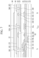
- FIG. 7 illustrates a cross-sectional view taken along line VII-VII of FIG. 6 .
- FIG. 6 and FIG. 7 differs from the embodiment of FIG. 4 and FIG. 5 in that the bottom shield layer BSL does not overlap the gate electrode of the driving transistor T 1 .
- the embodiment by using the flexible substrate, has an effect of preventing the channel of the driving transistor T 1 from being affected by an electric field based on polarity arrangement of molecules generated in the substrate 110 , which will be described in detail with reference to FIG. 8 to FIG. 10 .
- FIG. 8 illustrates a cross-sectional view of a pixel according to an embodiment.
- the flexible substrate 110 including the polyimide includes two polyimide layers 110 - 1 and 110 - 3 and two barrier layers 110 - 2 and 110 - 4 .
- Each of the barrier layers 110 - 2 and 110 - 4 is made of inorganic insulation materials such as a silicon nitride (SiNx), a silicon oxide (SiOx), and a silicon oxynitride (SiOxNy).
- a double-layered buffer layer 111 is disposed on the upper barrier layer 110 - 4 , one of a lower buffer layer 111 - 1 and an upper buffer layer 111 - 2 may be made of a silicon nitride (SiNx), and the other thereof may be made of a silicon oxide (SiOx).
- the bottom shield layer BSL is not covered with the buffer layer 111 , but is covered with the upper barrier layer 110 - 4 , and is formed on the upper polyimide layer 110 - 3 .
- the fifth or sixth transistor T 5 or T 6 has a structure of having a channel in the polycrystalline semiconductor layer and including a gate electrode disposed on the emission control line 155 .
- the third transistor T 3 has the channel 3137 in the oxide semiconductor layer, and the first/second areas 3136 and 3138 at respective sides of the channel 3137 .
- the third transistor T 3 includes the gate electrode 3151 overlapping the channel 3137 .
- the light blocking layer 3155 and the second connecting electrode 3175 may be included around the third transistor T 3 .
- the light blocking layer 3155 has a structure that overlaps the oxide semiconductor layer including the channel of the third transistor T 3 , and the second connection electrode 3175 is connected to the first area 3136 of the third transistor T 3 through the fourth opening 3166 .
- molecules molecules such as of a polyimide included in the upper polyimide layer 110 - 3 have a characteristic that they are arranged by an electric field.
- the present embodiment and a comparative example will be compared with respect to the electric field characteristic in the emission period with reference to FIG. 9 to FIG. 11 .
- FIG. 9 illustrates a cross-sectional view of a pixel according to a comparative example
- FIG. 10 and FIG. 11 illustrate electric field distributions of a pixel according to a comparative example.
- a comparative example of FIG. 9 is a structure without the bottom shield layer BSL as compared with the embodiment of FIG. 8 .
- FIG. 9 it can be seen that as the molecules are arranged in the upper polyimide layer 110 - 3 due to the negative voltage applied to the third transistor T 3 and the negative voltage applied to the fifth or sixth transistor T 5 or T 6 , the electric field is concentrated under the driving transistor T 1 . This is because a strong negative voltage is positioned at both sides, so that a relatively positive polarity should be caused therebetween, and the caused positive polarity is formed around a surface of the upper polyimide layer 110 - 3 .
- the bottom shield layer BLS is disposed on the surface of the upper polyimide layer 110 - 3 , so that charges of the positive polarity caused on the surface of the upper polyimide layer 110 - 3 are shielded by the bottom shield layer BSL to not affect the channel of the driving transistor T 1 . As a result, the characteristic of the driving transistor T 1 is not changed.
- a pixel (HOP pixel) using two types of semiconductor layers (polycrystalline semiconductor layer and oxide semiconductor layer) ( FIG. 10 ) and a pixel (LTPS pixel) using only a polycrystalline semiconductor layer as a semiconductor layer are compared and illustrated.
- FIG. 10 shows that when two different types of semiconductor layers are used, as in FIG. 9 , a voltage allowing one transistor to be turned on and a voltage allowing the other transistor to be turned off are the same, so that the electric field is concentrated on the driving transistor T 1 disposed therebetween.
- the opening FSA in the rear surface of the pixel that uses the structure in which the polycrystalline semiconductor layer and the oxide semiconductor layer are formed in one pixel, for fingerprint sensing and the like, it can be seen that it is necessary to form the bottom shield layer BSL in an area overlapping the opening FSA in a plan view due to light applied through the opening FSA and in pixels disposed around the area.
- FIG. 12 and FIG. 13 illustrate cross-sectional views of a pixel according to another embodiment
- FIG. 14 illustrates a layout view of a pixel according to another embodiment.
- a bottom shield layer BSL formed at a layer position that is different from that of FIG. 8 will be described through FIG. 12 and FIG. 13 .
- FIG. 12 illustrates an embodiment in which the bottom shield layer BSL is disposed on the upper barrier layer 110 - 4 and is covered by the buffer layer 111 , specifically, the lower buffer layer 111 - 1 .
- the bottom shield layer BSL may be formed on the lower buffer layer 111 - 1 , and may be covered by the upper buffer layer 111 - 2 .
- two bottom shield layers BSL (first bottom shield layer and second bottom shield layer) disposed around the channel of the driving transistor T 1 are formed, and one thereof is formed on the upper polyimide layer 110 - 3 and is covered by the upper barrier layer 110 - 4 , and the other thereof is disposed on the upper barrier layer 110 - 4 and is covered by the buffer layer 111 .
- the two bottom shield layers BSL shown in FIG. 13 may have a structure in which at least some areas overlap each other, and may have different shapes or the same shape.
- the bottom shield layer BSL may be floating, but in the structure shown in FIG. 14 , an extension connected to the bottom shield layer BSL formed in adjacent pixels is formed, so that the bottom shield layer BSL is not floating, and it may be applied with a voltage of a constant level (for example, the driving voltage ELVDD).
- the second display area DA 2 may be disposed in the second display area DA 2 in which a camera is positioned as shown in FIG. 15 .
- a second display area DA 2 will be described through FIG. 15 to FIG. 17 .
- the first display area DA 1 is an area in which the plurality of pixels PX are continuously arranged for displaying an image, the pixel circuit part of the pixel PX may be continuously arranged along rows and columns, and the light emitting elements may be arranged in various ways.
- the first display area DA 1 mainly displays an image, and may include a touch sensing electrode at an upper side thereof to sense a touch.
- the first display area DA 1 is not disposed at an upper portion of the second display area DA 2 , but in some embodiment, the second display area DA 2 may be surrounded by the first display area DA 1 .
- FIG. 16 illustrates that the window 250 and the touch sensing part 200 are disposed on the upper portion of the display panel 100 , but the window 250 and the touch sensing part 200 may be additionally included in FIG. 2 .
- FIG. 16 briefly illustrates that various elements of the pixel PX are formed on the flexible substrate 110 of the display panel 100 .
- the pixel PX of the display panel 100 may be covered by an encapsulation layer to be sealed to prevent moisture or air from penetrating from the outside.
- the second display area DA 2 includes the pixel area DA 2 - 1 and the transmission area DA 2 - 2 , and the transmission area DA 2 - 2 may be separated and partitioned by wires SL 1 and SL 2 connected to each other by the pixel area DA 2 - 1 .
- a polarizer may be attached to the upper surface of the display panel 100 , or a color filter layer or a color conversion layer may be further formed thereon together with a black matrix. These constituent elements may serve to prevent external light from being reflected and thus prevent the upper pattern of the pixel from being viewed by a user's eye. In addition, the color filter layer or the color conversion layer may be used to improve displayed color.
- the optical elements 25 may include a sensor, a camera, and a flash.
- the optical element 25 may be a proximity sensor, an illuminance sensor, an infrared sensor, or an ultraviolet sensor.
- FIG. 18 illustrates shapes of various bottom shield layers according to an embodiment.
- FIG. 18 A illustrates the bottom shield layer BSL including an upper portion that is opened
- FIG. 18 B illustrates the bottom shield layer BSL including both sides that are opened
- FIG. 18 C illustrates the bottom shield layer BSL including one side that is opened.
- a structure in which a lower portion thereof is opened or a left side thereof is opened may also be used.
- the bottom shield layer BSL having a linear structure is respectively formed at upper and lower sides of the channel of the driving transistor T 1 , but through modification, the bottom shield layer BSL having a linear structure may be formed only at one side of the upper and lower sides.
- a pixel including an optimized bottom shield layer BSL may be formed by selecting one of the various structures shown in FIG. 18 .
Landscapes
- Engineering & Computer Science (AREA)
- Chemical & Material Sciences (AREA)
- Inorganic Chemistry (AREA)
- Microelectronics & Electronic Packaging (AREA)
- Physics & Mathematics (AREA)
- Geometry (AREA)
- Life Sciences & Earth Sciences (AREA)
- Sustainable Development (AREA)
- Computer Hardware Design (AREA)
- General Physics & Mathematics (AREA)
- Theoretical Computer Science (AREA)
- Electroluminescent Light Sources (AREA)
- Devices For Indicating Variable Information By Combining Individual Elements (AREA)
Abstract
Description
Claims (20)
Applications Claiming Priority (2)
| Application Number | Priority Date | Filing Date | Title |
|---|---|---|---|
| KR10-2020-0159977 | 2020-11-25 | ||
| KR1020200159977A KR20220072930A (en) | 2020-11-25 | 2020-11-25 | Display device |
Publications (2)
| Publication Number | Publication Date |
|---|---|
| US20220165824A1 US20220165824A1 (en) | 2022-05-26 |
| US12185581B2 true US12185581B2 (en) | 2024-12-31 |
Family
ID=81657513
Family Applications (1)
| Application Number | Title | Priority Date | Filing Date |
|---|---|---|---|
| US17/376,064 Active 2043-04-16 US12185581B2 (en) | 2020-11-25 | 2021-07-14 | Display device including bottom shield layer disposed between polyimide layer and polycrystalline semiconductor layer |
Country Status (3)
| Country | Link |
|---|---|
| US (1) | US12185581B2 (en) |
| KR (1) | KR20220072930A (en) |
| CN (1) | CN114551504A (en) |
Families Citing this family (1)
| Publication number | Priority date | Publication date | Assignee | Title |
|---|---|---|---|---|
| KR20230072180A (en) * | 2021-11-17 | 2023-05-24 | 엘지디스플레이 주식회사 | Display device and display panel |
Citations (14)
| Publication number | Priority date | Publication date | Assignee | Title |
|---|---|---|---|---|
| US20020050795A1 (en) * | 2000-10-27 | 2002-05-02 | Nec Corporation | Active matrix organic el display device and method of forming the same |
| KR100742494B1 (en) | 2005-10-13 | 2007-07-24 | 산요덴키가부시키가이샤 | Thin film transistor and organic electroluminescence display device |
| JP5874804B2 (en) | 2010-02-15 | 2016-03-02 | Nltテクノロジー株式会社 | THIN FILM TRANSISTOR, ITS MANUFACTURING METHOD, DISPLAY DEVICE, AND ELECTRONIC DEVICE |
| US20170084636A1 (en) * | 2015-09-18 | 2017-03-23 | Hon Hai Precision Industry Co., Ltd. | Array substrate and display device and method for making the array substrate |
| US20170352711A1 (en) * | 2016-06-07 | 2017-12-07 | Shenzhen China Star Optoelectronics Technology Co. Ltd. | Manufacturing method of tft backplane and tft backplane |
| KR20190115166A (en) | 2018-03-30 | 2019-10-11 | 삼성디스플레이 주식회사 | Organic light emitting diode display device |
| KR20200029081A (en) | 2018-09-07 | 2020-03-18 | 삼성디스플레이 주식회사 | Display device |
| US20210049958A1 (en) | 2019-08-12 | 2021-02-18 | Samsung Display Co., Ltd. | Display device and method of driving the same |
| US20210074736A1 (en) * | 2019-09-05 | 2021-03-11 | Japan Display Inc. | Semiconductor device |
| US20210098549A1 (en) * | 2019-08-22 | 2021-04-01 | Wuhan China Star Optoelectronics Semiconductor Display Technology Co., Ltd. | Thin film transistor array substrate and organic light emitting diode panel |
| US20210202621A1 (en) * | 2019-12-31 | 2021-07-01 | Wuhan Tianma Micro-Electronics Co., Ltd. | Display panel and display device |
| US20210202645A1 (en) * | 2019-12-27 | 2021-07-01 | Lg Display Co., Ltd. | Light Emitting Display Device |
| US20210328071A1 (en) * | 2018-06-01 | 2021-10-21 | Boe Technology Group Co., Ltd. | Thin film transistor and fabrication method thereof, array substrate and fabrication method thereof |
| US20230013848A1 (en) * | 2020-05-20 | 2023-01-19 | Boe Technology Group Co., Ltd. | Display panel, method for manufacturing the same, and tiled screen |
-
2020
- 2020-11-25 KR KR1020200159977A patent/KR20220072930A/en active Pending
-
2021
- 2021-07-14 US US17/376,064 patent/US12185581B2/en active Active
- 2021-08-24 CN CN202110972490.1A patent/CN114551504A/en active Pending
Patent Citations (14)
| Publication number | Priority date | Publication date | Assignee | Title |
|---|---|---|---|---|
| US20020050795A1 (en) * | 2000-10-27 | 2002-05-02 | Nec Corporation | Active matrix organic el display device and method of forming the same |
| KR100742494B1 (en) | 2005-10-13 | 2007-07-24 | 산요덴키가부시키가이샤 | Thin film transistor and organic electroluminescence display device |
| JP5874804B2 (en) | 2010-02-15 | 2016-03-02 | Nltテクノロジー株式会社 | THIN FILM TRANSISTOR, ITS MANUFACTURING METHOD, DISPLAY DEVICE, AND ELECTRONIC DEVICE |
| US20170084636A1 (en) * | 2015-09-18 | 2017-03-23 | Hon Hai Precision Industry Co., Ltd. | Array substrate and display device and method for making the array substrate |
| US20170352711A1 (en) * | 2016-06-07 | 2017-12-07 | Shenzhen China Star Optoelectronics Technology Co. Ltd. | Manufacturing method of tft backplane and tft backplane |
| KR20190115166A (en) | 2018-03-30 | 2019-10-11 | 삼성디스플레이 주식회사 | Organic light emitting diode display device |
| US20210328071A1 (en) * | 2018-06-01 | 2021-10-21 | Boe Technology Group Co., Ltd. | Thin film transistor and fabrication method thereof, array substrate and fabrication method thereof |
| KR20200029081A (en) | 2018-09-07 | 2020-03-18 | 삼성디스플레이 주식회사 | Display device |
| US20210049958A1 (en) | 2019-08-12 | 2021-02-18 | Samsung Display Co., Ltd. | Display device and method of driving the same |
| US20210098549A1 (en) * | 2019-08-22 | 2021-04-01 | Wuhan China Star Optoelectronics Semiconductor Display Technology Co., Ltd. | Thin film transistor array substrate and organic light emitting diode panel |
| US20210074736A1 (en) * | 2019-09-05 | 2021-03-11 | Japan Display Inc. | Semiconductor device |
| US20210202645A1 (en) * | 2019-12-27 | 2021-07-01 | Lg Display Co., Ltd. | Light Emitting Display Device |
| US20210202621A1 (en) * | 2019-12-31 | 2021-07-01 | Wuhan Tianma Micro-Electronics Co., Ltd. | Display panel and display device |
| US20230013848A1 (en) * | 2020-05-20 | 2023-01-19 | Boe Technology Group Co., Ltd. | Display panel, method for manufacturing the same, and tiled screen |
Also Published As
| Publication number | Publication date |
|---|---|
| KR20220072930A (en) | 2022-06-03 |
| US20220165824A1 (en) | 2022-05-26 |
| CN114551504A (en) | 2022-05-27 |
Similar Documents
| Publication | Publication Date | Title |
|---|---|---|
| US20230060545A1 (en) | Display substrate and display device | |
| US7491969B2 (en) | Organic light emitting diode display | |
| US20160132148A1 (en) | Organic light-emitting diode (oled) display | |
| US20150090969A1 (en) | Display device | |
| US12213342B2 (en) | Display device and pixel array substrate thereof | |
| CN114551531A (en) | display device | |
| JP7111793B2 (en) | Pixel array substrate and display device having the same | |
| US20230380242A1 (en) | Display device | |
| EP4181650A1 (en) | Light emitting display device | |
| KR102892875B1 (en) | display panel and electric apparatus | |
| US12185581B2 (en) | Display device including bottom shield layer disposed between polyimide layer and polycrystalline semiconductor layer | |
| US12161030B2 (en) | Light emitting display device with transistor in transparent display area | |
| US11793039B2 (en) | Display device | |
| US20240304634A1 (en) | Light emitting display device | |
| US8581889B2 (en) | Display unit | |
| US20240147794A1 (en) | Light emitting display device | |
| US12550531B2 (en) | Light emitting display device | |
| US20240172512A1 (en) | Light emitting display device | |
| US20240282251A1 (en) | Display apparatus | |
| US20240130184A1 (en) | Display panel and electronic apparatus | |
| US20250212666A1 (en) | Display device | |
| US11289563B2 (en) | Electrode contact structure, display control driver, and display device | |
| CN119894296A (en) | Display device | |
| KR20240038900A (en) | Light emitting display device | |
| KR20240024398A (en) | Light emitting display device |
Legal Events
| Date | Code | Title | Description |
|---|---|---|---|
| AS | Assignment |
Owner name: SAMSUNG DISPLAY CO., LTD., KOREA, REPUBLIC OF Free format text: ASSIGNMENT OF ASSIGNORS INTEREST;ASSIGNOR:KIM, KEUN WOO;REEL/FRAME:056858/0346 Effective date: 20210603 |
|
| FEPP | Fee payment procedure |
Free format text: ENTITY STATUS SET TO UNDISCOUNTED (ORIGINAL EVENT CODE: BIG.); ENTITY STATUS OF PATENT OWNER: LARGE ENTITY |
|
| STPP | Information on status: patent application and granting procedure in general |
Free format text: DOCKETED NEW CASE - READY FOR EXAMINATION |
|
| STPP | Information on status: patent application and granting procedure in general |
Free format text: NON FINAL ACTION MAILED |
|
| STPP | Information on status: patent application and granting procedure in general |
Free format text: RESPONSE TO NON-FINAL OFFICE ACTION ENTERED AND FORWARDED TO EXAMINER |
|
| STPP | Information on status: patent application and granting procedure in general |
Free format text: NOTICE OF ALLOWANCE MAILED -- APPLICATION RECEIVED IN OFFICE OF PUBLICATIONS |
|
| STPP | Information on status: patent application and granting procedure in general |
Free format text: PUBLICATIONS -- ISSUE FEE PAYMENT VERIFIED |
|
| STCF | Information on status: patent grant |
Free format text: PATENTED CASE |