US12181799B2 - Resist compositions and semiconductor fabrication methods using the same - Google Patents
Resist compositions and semiconductor fabrication methods using the same Download PDFInfo
- Publication number
- US12181799B2 US12181799B2 US16/947,515 US202016947515A US12181799B2 US 12181799 B2 US12181799 B2 US 12181799B2 US 202016947515 A US202016947515 A US 202016947515A US 12181799 B2 US12181799 B2 US 12181799B2
- Authority
- US
- United States
- Prior art keywords
- halogen
- chemical formula
- substituted
- unsubstituted
- compound
- Prior art date
- Legal status (The legal status is an assumption and is not a legal conclusion. Google has not performed a legal analysis and makes no representation as to the accuracy of the status listed.)
- Active, expires
Links
Images


Classifications
-
- G—PHYSICS
- G03—PHOTOGRAPHY; CINEMATOGRAPHY; ANALOGOUS TECHNIQUES USING WAVES OTHER THAN OPTICAL WAVES; ELECTROGRAPHY; HOLOGRAPHY
- G03F—PHOTOMECHANICAL PRODUCTION OF TEXTURED OR PATTERNED SURFACES, e.g. FOR PRINTING, FOR PROCESSING OF SEMICONDUCTOR DEVICES; MATERIALS THEREFOR; ORIGINALS THEREFOR; APPARATUS SPECIALLY ADAPTED THEREFOR
- G03F7/00—Photomechanical, e.g. photolithographic, production of textured or patterned surfaces, e.g. printing surfaces; Materials therefor, e.g. comprising photoresists; Apparatus specially adapted therefor
- G03F7/004—Photosensitive materials
-
- C—CHEMISTRY; METALLURGY
- C07—ORGANIC CHEMISTRY
- C07C—ACYCLIC OR CARBOCYCLIC COMPOUNDS
- C07C25/00—Compounds containing at least one halogen atom bound to a six-membered aromatic ring
- C07C25/02—Monocyclic aromatic halogenated hydrocarbons
- C07C25/13—Monocyclic aromatic halogenated hydrocarbons containing fluorine
-
- G—PHYSICS
- G03—PHOTOGRAPHY; CINEMATOGRAPHY; ANALOGOUS TECHNIQUES USING WAVES OTHER THAN OPTICAL WAVES; ELECTROGRAPHY; HOLOGRAPHY
- G03F—PHOTOMECHANICAL PRODUCTION OF TEXTURED OR PATTERNED SURFACES, e.g. FOR PRINTING, FOR PROCESSING OF SEMICONDUCTOR DEVICES; MATERIALS THEREFOR; ORIGINALS THEREFOR; APPARATUS SPECIALLY ADAPTED THEREFOR
- G03F7/00—Photomechanical, e.g. photolithographic, production of textured or patterned surfaces, e.g. printing surfaces; Materials therefor, e.g. comprising photoresists; Apparatus specially adapted therefor
- G03F7/004—Photosensitive materials
- G03F7/0045—Photosensitive materials with organic non-macromolecular light-sensitive compounds not otherwise provided for, e.g. dissolution inhibitors
-
- G—PHYSICS
- G03—PHOTOGRAPHY; CINEMATOGRAPHY; ANALOGOUS TECHNIQUES USING WAVES OTHER THAN OPTICAL WAVES; ELECTROGRAPHY; HOLOGRAPHY
- G03F—PHOTOMECHANICAL PRODUCTION OF TEXTURED OR PATTERNED SURFACES, e.g. FOR PRINTING, FOR PROCESSING OF SEMICONDUCTOR DEVICES; MATERIALS THEREFOR; ORIGINALS THEREFOR; APPARATUS SPECIALLY ADAPTED THEREFOR
- G03F7/00—Photomechanical, e.g. photolithographic, production of textured or patterned surfaces, e.g. printing surfaces; Materials therefor, e.g. comprising photoresists; Apparatus specially adapted therefor
- G03F7/004—Photosensitive materials
- G03F7/027—Non-macromolecular photopolymerisable compounds having carbon-to-carbon double bonds, e.g. ethylenic compounds
- G03F7/028—Non-macromolecular photopolymerisable compounds having carbon-to-carbon double bonds, e.g. ethylenic compounds with photosensitivity-increasing substances, e.g. photoinitiators
- G03F7/029—Inorganic compounds; Onium compounds; Organic compounds having hetero atoms other than oxygen, nitrogen or sulfur
- G03F7/0295—Photolytic halogen compounds
-
- G—PHYSICS
- G03—PHOTOGRAPHY; CINEMATOGRAPHY; ANALOGOUS TECHNIQUES USING WAVES OTHER THAN OPTICAL WAVES; ELECTROGRAPHY; HOLOGRAPHY
- G03F—PHOTOMECHANICAL PRODUCTION OF TEXTURED OR PATTERNED SURFACES, e.g. FOR PRINTING, FOR PROCESSING OF SEMICONDUCTOR DEVICES; MATERIALS THEREFOR; ORIGINALS THEREFOR; APPARATUS SPECIALLY ADAPTED THEREFOR
- G03F7/00—Photomechanical, e.g. photolithographic, production of textured or patterned surfaces, e.g. printing surfaces; Materials therefor, e.g. comprising photoresists; Apparatus specially adapted therefor
- G03F7/004—Photosensitive materials
- G03F7/038—Macromolecular compounds which are rendered insoluble or differentially wettable
- G03F7/0382—Macromolecular compounds which are rendered insoluble or differentially wettable the macromolecular compound being present in a chemically amplified negative photoresist composition
-
- G—PHYSICS
- G03—PHOTOGRAPHY; CINEMATOGRAPHY; ANALOGOUS TECHNIQUES USING WAVES OTHER THAN OPTICAL WAVES; ELECTROGRAPHY; HOLOGRAPHY
- G03F—PHOTOMECHANICAL PRODUCTION OF TEXTURED OR PATTERNED SURFACES, e.g. FOR PRINTING, FOR PROCESSING OF SEMICONDUCTOR DEVICES; MATERIALS THEREFOR; ORIGINALS THEREFOR; APPARATUS SPECIALLY ADAPTED THEREFOR
- G03F7/00—Photomechanical, e.g. photolithographic, production of textured or patterned surfaces, e.g. printing surfaces; Materials therefor, e.g. comprising photoresists; Apparatus specially adapted therefor
- G03F7/004—Photosensitive materials
- G03F7/039—Macromolecular compounds which are photodegradable, e.g. positive electron resists
- G03F7/0392—Macromolecular compounds which are photodegradable, e.g. positive electron resists the macromolecular compound being present in a chemically amplified positive photoresist composition
-
- G—PHYSICS
- G03—PHOTOGRAPHY; CINEMATOGRAPHY; ANALOGOUS TECHNIQUES USING WAVES OTHER THAN OPTICAL WAVES; ELECTROGRAPHY; HOLOGRAPHY
- G03F—PHOTOMECHANICAL PRODUCTION OF TEXTURED OR PATTERNED SURFACES, e.g. FOR PRINTING, FOR PROCESSING OF SEMICONDUCTOR DEVICES; MATERIALS THEREFOR; ORIGINALS THEREFOR; APPARATUS SPECIALLY ADAPTED THEREFOR
- G03F7/00—Photomechanical, e.g. photolithographic, production of textured or patterned surfaces, e.g. printing surfaces; Materials therefor, e.g. comprising photoresists; Apparatus specially adapted therefor
- G03F7/20—Exposure; Apparatus therefor
- G03F7/2002—Exposure; Apparatus therefor with visible light or UV light, through an original having an opaque pattern on a transparent support, e.g. film printing, projection printing; by reflection of visible or UV light from an original such as a printed image
- G03F7/2012—Exposure; Apparatus therefor with visible light or UV light, through an original having an opaque pattern on a transparent support, e.g. film printing, projection printing; by reflection of visible or UV light from an original such as a printed image using liquid photohardening compositions, e.g. for the production of reliefs such as flexographic plates or stamps
-
- G—PHYSICS
- G03—PHOTOGRAPHY; CINEMATOGRAPHY; ANALOGOUS TECHNIQUES USING WAVES OTHER THAN OPTICAL WAVES; ELECTROGRAPHY; HOLOGRAPHY
- G03F—PHOTOMECHANICAL PRODUCTION OF TEXTURED OR PATTERNED SURFACES, e.g. FOR PRINTING, FOR PROCESSING OF SEMICONDUCTOR DEVICES; MATERIALS THEREFOR; ORIGINALS THEREFOR; APPARATUS SPECIALLY ADAPTED THEREFOR
- G03F7/00—Photomechanical, e.g. photolithographic, production of textured or patterned surfaces, e.g. printing surfaces; Materials therefor, e.g. comprising photoresists; Apparatus specially adapted therefor
- G03F7/20—Exposure; Apparatus therefor
- G03F7/2037—Exposure with X-ray radiation or corpuscular radiation, through a mask with a pattern opaque to that radiation
- G03F7/2039—X-ray radiation
-
- G—PHYSICS
- G03—PHOTOGRAPHY; CINEMATOGRAPHY; ANALOGOUS TECHNIQUES USING WAVES OTHER THAN OPTICAL WAVES; ELECTROGRAPHY; HOLOGRAPHY
- G03F—PHOTOMECHANICAL PRODUCTION OF TEXTURED OR PATTERNED SURFACES, e.g. FOR PRINTING, FOR PROCESSING OF SEMICONDUCTOR DEVICES; MATERIALS THEREFOR; ORIGINALS THEREFOR; APPARATUS SPECIALLY ADAPTED THEREFOR
- G03F7/00—Photomechanical, e.g. photolithographic, production of textured or patterned surfaces, e.g. printing surfaces; Materials therefor, e.g. comprising photoresists; Apparatus specially adapted therefor
- G03F7/20—Exposure; Apparatus therefor
- G03F7/2051—Exposure without an original mask, e.g. using a programmed deflection of a point source, by scanning, by drawing with a light beam, using an addressed light or corpuscular source
- G03F7/2059—Exposure without an original mask, e.g. using a programmed deflection of a point source, by scanning, by drawing with a light beam, using an addressed light or corpuscular source using a scanning corpuscular radiation beam, e.g. an electron beam
-
- G—PHYSICS
- G03—PHOTOGRAPHY; CINEMATOGRAPHY; ANALOGOUS TECHNIQUES USING WAVES OTHER THAN OPTICAL WAVES; ELECTROGRAPHY; HOLOGRAPHY
- G03F—PHOTOMECHANICAL PRODUCTION OF TEXTURED OR PATTERNED SURFACES, e.g. FOR PRINTING, FOR PROCESSING OF SEMICONDUCTOR DEVICES; MATERIALS THEREFOR; ORIGINALS THEREFOR; APPARATUS SPECIALLY ADAPTED THEREFOR
- G03F7/00—Photomechanical, e.g. photolithographic, production of textured or patterned surfaces, e.g. printing surfaces; Materials therefor, e.g. comprising photoresists; Apparatus specially adapted therefor
- G03F7/26—Processing photosensitive materials; Apparatus therefor
- G03F7/42—Stripping or agents therefor
-
- G—PHYSICS
- G03—PHOTOGRAPHY; CINEMATOGRAPHY; ANALOGOUS TECHNIQUES USING WAVES OTHER THAN OPTICAL WAVES; ELECTROGRAPHY; HOLOGRAPHY
- G03F—PHOTOMECHANICAL PRODUCTION OF TEXTURED OR PATTERNED SURFACES, e.g. FOR PRINTING, FOR PROCESSING OF SEMICONDUCTOR DEVICES; MATERIALS THEREFOR; ORIGINALS THEREFOR; APPARATUS SPECIALLY ADAPTED THEREFOR
- G03F7/00—Photomechanical, e.g. photolithographic, production of textured or patterned surfaces, e.g. printing surfaces; Materials therefor, e.g. comprising photoresists; Apparatus specially adapted therefor
- G03F7/70—Microphotolithographic exposure; Apparatus therefor
- G03F7/70008—Production of exposure light, i.e. light sources
- G03F7/70033—Production of exposure light, i.e. light sources by plasma extreme ultraviolet [EUV] sources
-
- H01L21/0274—
-
- H—ELECTRICITY
- H10—SEMICONDUCTOR DEVICES; ELECTRIC SOLID-STATE DEVICES NOT OTHERWISE PROVIDED FOR
- H10P—GENERIC PROCESSES OR APPARATUS FOR THE MANUFACTURE OR TREATMENT OF DEVICES COVERED BY CLASS H10
- H10P76/00—Manufacture or treatment of masks on semiconductor bodies, e.g. by lithography or photolithography
- H10P76/20—Manufacture or treatment of masks on semiconductor bodies, e.g. by lithography or photolithography of masks comprising organic materials
- H10P76/204—Manufacture or treatment of masks on semiconductor bodies, e.g. by lithography or photolithography of masks comprising organic materials of organic photoresist masks
- H10P76/2041—Photolithographic processes
Definitions
- the present inventive concepts relate to a resist composition and a pattern formation method using the same, and more particularly, to an extreme ultraviolet photoresist composition and a pattern formation method using the same.
- Semiconductor devices have been highly integrated for high performance and low manufacture costs.
- An increase in integration of semiconductor devices may be achieved by precise patterning layers during fabricating semiconductor devices. Exposure and development processes using photoresist layers may be performed to pattern layers.
- Some example embodiments of the present inventive concepts provide a semiconductor device fabrication method with increased precision for a patterning process.
- Some example embodiments of the present inventive concepts provide a pattern formation method in which a fine pitch pattern is formed with high accuracy.
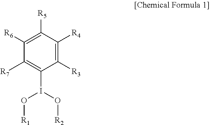
- a resist composition may include a hypervalent iodine compound of Chemical Formula 1 below.
- R 1 may be hydrogen, R 8 CO 2 ⁇ , or R 9 SO 2 ⁇ .
- R 2 may be R 10 CO 2 ⁇ or R 11 SO 2 ⁇ .
- R 3 , R 4 , R 5 , R 6 , and R 7 may each independently be a hydrogen, a halogen, a halogen-substituted C1 or C2 alkyl group, or a halogen-substituted C6 to C20 aryl group.
- R 8 , R 9 , R 10 , and R 11 may each independently be a substituted or unsubstituted C1 or C2 alkyl group or a substituted or unsubstituted C6 to C20 aryl group.
- a semiconductor device fabrication method may include: coating on a substrate a composition to form a resist layer; and patterning the resist layer.
- the composition may include a hypervalent iodine compound of Chemical Formula 1 below.
- R 1 may be a hydrogen, R 8 CO 2 ⁇ , or R 9 SO 2 ⁇ .
- R 2 may be R 10 CO 2 ⁇ or R 11 SO 2 ⁇ .
- R 3 , R 4 , R 5 , R 6 , and R 7 may each be hydrogen.
- R 8 and R 9 may each be independently a halogen-substituted or halogen-unsubstituted C1 or C2 alkyl group or a halogen-substituted or halogen-unsubstituted C6 to C20 aryl group.
- R 10 may be an unsubstituted C1 or C2 alkyl group or an unsubstituted C6 to C20 aryl group.
- R 11 may be a halogen-substituted or halogen-unsubstituted C1 or C2 alkyl group or a halogen-substituted or halogen-unsubstituted C6 to C20 aryl group.
- FIG. 1 illustrates a graph showing EUV absorption intensity of compounds of Chemical Formulae M1 to M5 and Comparative Examples.
- FIG. 2 illustrates a graph showing dissociation energy of compounds of Chemical Formulae M1 to M5 and Comparative Examples.
- FIG. 3 illustrates a graph showing electron-trap decomposition energy of compounds of Chemical Formulae M1 to M5 and Comparative Examples.
- FIG. 4 illustrates a plan view showing a resist pattern according to some example embodiments of the present inventive concepts.
- FIGS. 5 to 8 illustrate cross-sectional views showing a semiconductor device fabrication method according to some example embodiments of the present inventive concepts.
- FIGS. 9 and 10 illustrate cross-sectional views showing a semiconductor device fabrication method according to some example embodiments of the present inventive concepts.
- the language “unsubstituted or substituted” may mean “unsubstituted or substituted with at least one substituent selected from deuterium atoms, halogen atoms, hydroxyl group, alkoxy group, ether group, halogenated alkyl group, halogenated alkoxy group, halogenated ether group, alkyl group, alkenyl group, aryl group, cyclic hydrocarbon group, and heterocyclic group.
- each substituent mentioned above may be substituted or unsubstituted.
- a halogenated alkyl group may be referred to as an alkyl group.
- a halogen element may be fluorine, chlorine, iodine, or bromine.
- an alkyl group may be a straight, branched, or cyclic alkyl group.
- the number of carbon atoms in an alkyl group may be 1 or 2 (also referred to herein as a C1 or C2 alkyl group), but the present inventive concepts are not limited thereto.
- Examples of an alkyl group may be a methyl group and an ethyl group, but the present inventive concepts are not limited thereto.
- an aryl group may include a substituted or unsubstituted aryl group.
- the number of carbon atoms in an aryl group may be 6 to 20 (also referred to herein as a C6 to C20 aryl group).
- composition a composition, a pattern formation method using the composition, and a semiconductor device fabrication method using the composition.
- the composition may be a resist composition.
- the composition may be used to form patterns or to fabricate semiconductor devices.
- the resist composition may be used in patterning processes for semiconductor device fabrication.
- the resist composition may be an extreme ultraviolet (EUV) resist composition or an electron-beam resist composition.
- EUV may refer to an ultraviolet ray whose wavelength falls within a range of about 10 nm to about 124 nm, more narrowly of about 13.0 nm to about 13.9 nm, much more narrowly of about 13.4 nm to about 13.6 nm.
- the EUV may refer to light whose energy ranges from about 6.21 eV to about 124 eV, more narrowly about 90 eV to about 95 eV.
- the resist composition according to some embodiments may be a chemical amplified resist (CAR) type composition.
- the resist composition may include a polymer and a hypervalent iodine compound.
- the resist composition may further include a quencher.
- the hypervalent iodine compound may be a compound of Chemical Formula 1 below.
- R 1 may be hydrogen, R 8 CO 2 ⁇ , or R 9 SO 2 ⁇ ;
- R 2 may be R 10 CO 2 ⁇ or R 11 SO 2 ⁇ ;
- R 3 , R 4 , R 5 , R 6 , and R 7 may each independently be a hydrogen, a halogen, a halogen-substituted C1 or C2 alkyl group, or a halogen-substituted C6 to C20 aryl group; and
- R 8 , R 9 , R 10 , and R 11 may each independently be a substituted or unsubstituted C1 or C2 alkyl group or a substituted or unsubstituted C6 to C20 aryl group.
- the substituted alkyl group may include a halogen-substituted alkyl group
- the substituted aryl group may include a halogen-substituted aryl group
- R 1 and R 2 may include no hydrogen.
- R 1 may include R 8 CO 2 ⁇ or R 9 SO 2 ⁇
- R 2 may include R 10 CO 2 ⁇ or R 11 SO 2 ⁇
- R 8 , R 9 , R 10 , and R 11 may be the same as those defined above.
- the polymer may be a photoresist material.
- the polymer may include a compound of Chemical Formula 2A below, but the present inventive concepts are not limited thereto.
- R 20 , R 21 , and R 22 may each independently be hydrogen or a substituted or unsubstituted C1 to C15 alkyl group, and m may be an integer between 10 and 1,000,000.
- the polymer may include a compound of Chemical Formula 2B below.
- n may be an integer of from 10 to 1,000.
- the resist composition may further include a photo-acid generator.
- the photo-acid generator may generate hydrogen ions in a subsequent exposure process.
- the photo-acid generator may include one or more of a compound of Chemical Formula 3A below and a compound of Chemical Formula 3B below.
- the material represented by Chemical Formula 3A may be referred to as diphenyliodonium triflate (DPT-Tf), and the material represented by Chemical Formula 3B may be referred to as triphenylsulfonium triflate (TPS-Tf).
- the resist composition may further include the photo-acid generator.
- the resist composition may include no additional photo-acid generator.
- the resist composition may further include the compound of Chemical Formula 3A and/or the compound of Chemical Formula 3B.
- the quencher may be, for example, a photo-decomposable quencher (PDQ).
- the quencher may include a base material.
- the quencher may include an amine, for example, a tertiary amine.
- the tertiary amine may include 10 to 100 carbon atoms, but the present inventive concepts are not limited thereto.
- the quencher may include, for example, one or more of a compound of Chemical Formula 4A below and a compound of Chemical Formula 4B below.
- the compound of Chemical Formula 4A may be tri (n-octyl) amine.
- the compound of Chemical Formula 4B may be 1,8-diazabicyclo[5.4.0]undec-7-ene (DBU).
- R 1 may be hydrogen, R 8 CO 2 ⁇ or R 9 SO 2 ⁇
- R 2 may be R 10 CO 2 ⁇ or R 11 SO 2 ⁇
- R 3 , R 4 , R 5 , R 6 , and R 7 may each independently be hydrogen
- R 8 and R 9 may each independently be a halogen-substituted or halogen-unsubstituted C1 or C2 alkyl group or a halogen-substituted or halogen-unsubstituted C6 to C20 aryl group
- R 10 may be an unsubstituted C1 or C2 alkyl group or an unsubstituted C6 to C20 aryl group
- R 11 may be a halogen-substituted or halogen-unsubstituted C1 or C2 alkyl group or a halogen-substituted or halogen-unsubstituted C6 to C20 aryl group.
- the hypervalent iodine compound of Chemical Formula 1 may serve as an additive.
- the hypervalent iodine compound may have a high LUMO (lowest unoccupied molecular orbital) energy level.
- the polymer may absorb light to emit secondary electrons. The light may be an extreme ultraviolet ray.
- One or more of the secondary electrons may be transferred and trapped by the photo-acid generator.
- the photo-acid generator may decompose the transferred secondary electrons and may generate hydrogen ions (H + ). Under the presence of the secondary electron and the photo-acid generator, the hypervalent iodine compound may act as an acid to accelerate the generation of hydrogen ions.
- An exposure process of a resist layer may mainly depend on transfer efficiency of the secondary electron. For example, an increase in the transfer efficiency of the secondary electron may improve patterning precision and accuracy.
- the hypervalent iodine compound may cause an enhancement in transfer efficiency of the secondary electron.
- an increase in generation of the secondary electron may improve efficiency and accuracy of the exposure process. Because the hypervalent iodine compound has high light absorption, the hypervalent iodine compound may absorb light to increase generation of the secondary electron.
- the compound of Chemical Formula 1 may be one of compounds of Chemical Formulae M1, M2, and M3 below.
- Each of the hypervalent iodine compounds of Chemical Formulae M1, M2, and M3 may serve as an additive.
- Table 1 lists LUMO energy levels of the compound of Chemical Formula M1, the compound of Chemical Formula M2, the compound of Chemical Formula M3, and the photo-acid generator.
- Embodiment Chemical Formula M1 ⁇ 1.03 Chemical Formula M2 ⁇ 0.89 Chemical Formula M3 ⁇ 0.89 Photo-acid diphenyliodonium triflate (DPT-Tf) ⁇ 1.31 generator triphenylsulfonium triflate (TPS-Tf) ⁇ 1.13
- the hypervalent iodine compound may have a high LUMO energy level.
- Each of the compounds of Chemical Formulae M1, M2, and M3 may have an LUMO energy level higher than that of the photo-acid generator.
- the hypervalent iodine compound may have the LUMO energy level higher than that of diphenyliodonium triflate and that of triphenylsulfonium triflate.
- the LUMO energy level of the hypervalent iodine compound may be equal to or greater than about ⁇ 1.12 eV. Therefore, the hypervalent iodine compound may accelerate transfer of the secondary electron toward the photo-acid generator.
- the hypervalent iodine compound When the hypervalent iodine compound has a LUMO energy level (e.g., less than about ⁇ 1.12 eV) lower than that of the photo-acid generator, the hypervalent iodine compound may not assist the transfer of the secondary electron.
- a LUMO energy level e.g., less than about ⁇ 1.12 eV
- the hypervalent iodine compound may have electron-trap decomposition properties, and thus may be decomposed to generate hydrogen ions under secondary-electron trap condition.
- the hypervalent iodine compound may have stability against heat and chemicals in performing an exposure process on a resist layer.
- the hypervalent iodine compound may have a conjugation structure. Therefore, the hypervalent iodine compound may have excellent interaction with one or more of the polymer and the photo-acid generator.
- Table 2 shows binding energies between the hypervalent iodine compound and the photo-acid generator.
- the binding energy may be intermolecular interaction energy between the hypervalent iodine compound and the photo-acid generator.
- the binding energy may not be covalent bond energy.
- the binding energy between the hypervalent iodine compound and the photo-acid generator may be equal to or greater than about 15.4 Kcal/mol.
- the hypervalent iodine compound When the binding energy between the hypervalent iodine compound and the photo-acid generator satisfies the condition above, the hypervalent iodine compound may have excellent interaction with the photo-acid generator, and the secondary electron may be effectively transferred through the hypervalent iodine compound toward the photo-acid generator.
- the binding energy satisfies the condition above, although the resist composition includes the hypervalent iodine compound and the photo-acid generator, no phase separation may occur between the hypervalent iodine compound and iodine.
- R 1 may be R 8 CO 2 — or R 9 SO 2 —
- R 2 may be R 10 CO 2 ⁇ or R 11 SO 2 ⁇
- R 3 , R 4 , R 5 , R 6 , and R 7 may each independently be hydrogen, halogen, a halogen-substituted C1 or C2 alkyl group, or a halogen-substituted C6 to C20 aryl group
- R 8 , R 9 , R 10 , and R 11 may each independently be a halogen-substituted or unsubstituted C1 or C2 alkyl group or a halogen-substituted or unsubstituted C6 to C20 aryl group.
- the hypervalent iodine compound of Chemical Formula 1 may serve as a photo-acid generator, and thus may generate hydrogen ions in performing an exposure process on a resist layer.
- a hypervalent iodine compound of Chemical Formula M4 below and a hypervalent iodine compound of Chemical Formula M5 below may each serve as a photo-acid generator.
- the hypervalent iodine compound may have a low LUMO energy level.
- the compound of Chemical Formula 1 may have the LUMO energy level lower than that of diphenyliodonium triflate and that of triphenylsulfonium triflate.
- the hypervalent iodine compound may have dissociation energy properties. Therefore, in performing an exposure process on a resist layer, the hypervalent iodine compound may be decomposed by the secondary electron, thereby generating hydrogen ions.
- the compound represented by Chemical Formula 1 may include a compound of Chemical Formula M4 or Chemical Formula M5.
- the hypervalent iodine compound of Chemical Formula M4 and the hypervalent iodine compound of Chemical Formula M5 may each serve as a photo-acid generator.
- Table 3 lists LUMO energy levels of the compound of Chemical Formula M4, of the compound of Chemical Formula M5, and of the photo-acid generator.
- the hypervalent iodine compound may have an LUMO energy level lower than that of diphenyliodonium triflate and that of triphenylsulfonium triflate.
- the compound of Chemical Formula M4 and the compound of Chemical Formula M5 may each have the LUMO energy level equal to or less than about ⁇ 1.14 eV. Therefore, in comparison with diphenyliodonium triflate and triphenylsulfonium triflate, the hypervalent iodine compound may readily receive the secondary electron.
- the hypervalent iodine compound When the hypervalent iodine compound has a LUMO energy level (e.g., greater than about ⁇ 1.14 eV) higher than that of the photo-acid generator, the hypervalent iodine compound may not act as a photo-acid generator.
- a LUMO energy level e.g., greater than about ⁇ 1.14 eV
- the following will describe detailed properties of the hypervalent iodine compound according to some example embodiments.
- the below-described properties of the hypervalent iodine compound may be applicable when the hypervalent iodine compound serves as an additive in a composition and when the hypervalent iodine compound serves as a photo-acid generator.
- the below-described properties of the hypervalent iodine compound may indicate properties of each of the compounds of Chemical Formulae M1 to M5.
- an increase in generation of the secondary electron may improve efficiency and accuracy of the exposure process.
- the hypervalent iodine compound may have improved EUV absorption properties.
- the EUV absorption properties may be evaluated with EUV absorption coefficient.
- FIG. 1 illustrates a graph showing EUV absorption intensity of compounds of Chemical Formulae M1 to M5 and Comparative Examples.
- the symbols M1, M2, M3, M4, and M5 refer to the compounds of Chemical Formulae M1, M2, M3, M4, and M5, respectively, and Comparative Examples may include diphenyliodonium triflate represented as R1, triphenylsulfonium triflate represented as R2, and phenol represented as R3.
- the compounds M1 to M5 of Chemical Formulae M1 to M5 may have their EUV absorption intensity greater than that of R3 (i.e., phenol).
- the compounds M4 and M5 of Chemical Formulae M4 and M5 may have their EUV absorption intensity greater than that of R1 (i.e., diphenyliodonium triflate) and that of R2 (i.e., triphenylsulfonium triflate). Because the compounds M4 and M5 of Chemical Formulae M4 and M5 have their high EUV absorption intensity, the resist composition may excellently absorb light in an EUV wavelength range during an exposure process.
- the hypervalent iodine compound may be stable in the chemical environment.
- the phrase “is stable in the chemical environment” may mean that there is no or extremely low reactivity with respect to the atmosphere, a dimethyl sulfoxide (DMSO) solution, an amine-containing material such as a trimethyl amine solution, and a cresol solution.
- DMSO dimethyl sulfoxide
- the language “atmosphere” may be defined to include about 80% nitrogen (N 2 ) and about 20% oxygen (O 2 ).
- the reactivity may be evaluated with dissociation energy.
- a dissociation reaction may cause the hypervalent iodine compound to produce cations and anions.
- the dissociation reaction of the hypervalent iodine compound may be shown as Equation 1 below.
- dissociation reaction energy may be defined as the dissociation energy.
- R 1 to R 7 may be the same as those defined herein in Chemical Formula 1.
- Equation 1A the dissociation reaction of the compound of Chemical Formula M2 may be shown as Equation 1A below.
- FIG. 2 illustrates a graph showing dissociation energies of compounds of Chemical Formulae M1 to M5 and Comparative Examples.
- the symbols M1, M2, M3, M4, and M5 may refer to the compounds of Chemical Formulae M1, M2, M3, M4, and M5, respectively, and Comparative Examples may include diphenyliodonium triflate represented as R1 and triphenylsulfonium triflate represented as R2.
- the dissociation energy may be a result obtained by subtracting energy of a starting material from a sum of energies of the produced cations and anions.
- the compounds M1 to M5 of Chemical Formulae M1 to M5 may have their dissociation energy greater than that of R1 (i.e., diphenyliodonium triflate) and that of R2 (i.e., triphenylsulfonium triflate).
- R1 i.e., diphenyliodonium triflate
- R2 i.e., triphenylsulfonium triflate
- This property that the compounds M1 to M5 of Chemical Formulae M1 to M5 have their large dissociation energy may be found in the atmosphere, a dimethyl sulfoxide (DMSO) solution, an amine-containing material such as a trimethyl amine solution, and a cresol solution.
- DMSO dimethyl sulfoxide
- amine-containing material such as a trimethyl amine solution
- cresol solution a cresol solution.
- Each of the compounds M1 to M5 of Chemical Formulae M1 to M5 may be dissociated to produce
- the compounds M1 to M5 of Chemical Formulae M1 to M5 may have their relatively large dissociation energy. It may be ascertained that the compounds M1 to M5 of Chemical Formulae M1 to M5 may have their superior stability in various chemical environments.
- the hypervalent iodine compound may be thermally stable.
- Table 4 lists melting points of the compounds of Chemical Formulae M1 to M5.
- the hypervalent iodine compound may have a relatively high melting point.
- the hypervalent iodine compound may have a solid or crystalline state at room temperature (e.g., about 25° C.).
- the hypervalent iodine compound may have a melting point of, for example, greater than about 100° C. Therefore, the hypervalent iodine compound may be thermally stable.
- the hypervalent iodine compound may react with the polymer or the photo-acid generator under secondary-electron trap condition, thereby producing hydrogen ions.
- the hypervalent iodine compound may serve to produce acid.
- Equation 2 a reaction for the hydrogen ion generation from the hypervalent iodine compound may be shown in Equation 2 below.
- R 1 to R 7 may be the same as those defined herein in Chemical Formula 1, e ⁇ may be the secondary electron, RH may be one of the polymer of Chemical Formula 2A, the polymer of Chemical Formula 2B, diphenyliodonium triflate, and triphenylsulfonium triflate.
- Equation 2A a reaction for the hydrogen ion generation from the compound of Chemical Formula M2 may be shown as Equation 2A below.
- Equation 2A e ⁇ may be the secondary electron, and RH may be one of the polymer of Chemical Formula 2A, the polymer of Chemical Formula 2B, diphenyliodonium triflate, and triphenylsulfonium triflate.
- FIG. 3 illustrates a graph showing electron-trap decomposition energy E ETD of compounds of Chemical Formulae M1 to M5 and Comparative Examples.
- the symbols M1, M2, M3, M4, and M5 may refer to the compounds of Chemical Formulae M1, M2, M3, M4, and M5, respectively, and Comparative Examples may include R1 (i.e., diphenyliodonium triflate) and R2 (i.e., triphenylsulfonium triflate).
- the electron-trap decomposition energy may be a result obtained by subtracting energy of a target material at its excited state from a total sum of energies of materials produced after decomposition.
- the compounds M1 to M5 of Chemical Formulae M1 to M5 may have their electron-trap decomposition energy of about ⁇ 25 Kcal/mol or less.
- the compounds M1 to M5 of Chemical Formulae M1 to M5 may have their hydrogen-trap decomposition energy whose negative value is less than that of hydrogen-trap energy.
- the compounds M1 to M5 of Chemical Formulae M1 to M5 may have their electron-trap decomposition energy whose negative value is less than that of electron-trap decomposition energy of R1 (i.e., diphenyliodonium triflate).
- an increase in transfer efficiency of the secondary electron may improve patterning precision and accuracy.
- the compounds M1 to M5 of Chemical Formulae M1 to M5 may be promptly decomposed due to their reaction with the secondary electron, thereby producing hydrogen ions. Because the compounds M1 to M5 of Chemical Formulae M1 to M5 promptly react with the secondary electron, the secondary electron may increase in transfer efficiency.
- FIG. 4 illustrates a plan view showing a resist pattern according to some example embodiments of the present inventive concepts.
- FIGS. 5 to 8 illustrate cross-sectional views taken along line I-II of FIG. 4 , showing a semiconductor device fabrication method according to some example embodiments of the present inventive concepts.
- a substrate 100 may be prepared.
- a lower layer 200 and a resist layer 300 may be sequentially formed on the substrate 100 .
- the lower layer 200 may be an etching target.
- the lower layer 200 may include a semiconductor material, a conductive material, a dielectric material, or any combination thereof.
- the lower layer 200 may be formed of a single layer or a plurality of stacked layers. Although not shown, one or more layers may further be provided between the substrate 100 and the lower layer 200 .
- a resist composition (or a resist compound) may be coated on the lower layer 200 , thereby forming the resist layer 300 .
- a spin coating process may be performed to coat the resist composition.
- An annealing process may be further performed on the coated resist compound. The annealing process may correspond to a baking process of the resist layer 300 .
- the resist layer 300 may be exposed to light 500 .
- the light 500 may be an electron beam or an extreme ultraviolet ray.
- a photomask 400 may be disposed on the resist layer 300 .
- the resist layer 300 may have a first portion 310 exposed by the photomask 400 , and the light 500 may be irradiated on the first portion 310 of the resist layer 300 .
- a polymer may absorb the light 500 to emit secondary electrons.
- An efficiency increase in generation and transfer of the secondary electron may result in a precise formation of the first portion 310 and an increase in efficiency of the exposure process.
- a hypervalent iodine compound may include an iodine atom and may exhibit high extreme ultraviolet (EUV) adsorption.
- the secondary electrons may be transferred and trapped by a photo-acid generator.
- the photo-acid generator may decompose the transferred second electrons and may generate hydrogen ions (H + ).
- the hypervalent iodine compound may react with the secondary electron, thereby generating the hydrogen ion.
- the hypervalent iodine compound may enhance transfer efficiency of the secondary electron. Because the resist composition includes the hypervalent iodine compound, the first portion 310 of the resist layer 300 may be promptly formed and may have a fine width.
- a second portion 320 of the resist layer 300 may not be exposed to the light 500 .
- the resist compound contained in the second portion 320 of the resist layer 300 may have an unchanged chemical structure. Therefore, after the irradiation of the light 500 , the first portion 310 of the resist layer 300 may have a chemical structure different from that of the second portion 320 . Thereafter, the photomask 400 may be removed.
- a developer may remove the second portion 320 of the resist layer 300 , thereby forming a resist pattern 300 P.
- the resist pattern 300 P may be formed by a patterning process that includes exposure and development processes.
- the resist pattern 300 P may correspond to the first portion 310 of the resist layer 300 .
- the resist pattern 300 P may be formed to have a fine width W and pitch.
- the resist pattern 300 P may have a linear shape when viewed in plan as shown in FIG. 4 .
- the resist pattern 300 P may include extensions elongated in one direction.
- the resist pattern 300 P may have various shapes such as a zigzag shape, a honeycomb shape, or a circular shape, when viewed in plan.
- the resist pattern 300 P may expose the lower layer 200 .
- the lower layer 200 exposed by the resist pattern 300 P may be removed to form a lower pattern 200 P.
- An etching process may be performed to remove portions of the lower layer 200 .
- the lower layer 200 may have an etch selectivity with respect to the resist pattern 300 P.
- the lower pattern 200 P may expose the substrate 100 .
- the lower pattern 200 P may expose a layer interposed between the substrate 100 and the lower pattern 200 P.
- the resist pattern 300 P may be removed. Accordingly, the formation of a pattern may be completed.
- the pattern may indicate the lower pattern 200 P.
- the lower pattern 200 P may have a width that corresponds to the width W of the resist pattern 300 P. Because the resist pattern 300 P has the small width W, the lower pattern 200 P may be formed to have a small width.
- the processes mentioned above may complete the patterning of the lower layer 200 and the formation of the lower pattern 200 P.
- the lower pattern 200 P may be a component of a semiconductor device.
- the lower pattern 200 P may be a semiconductor pattern, a conductive pattern, or a dielectric pattern of the semiconductor device.
- FIGS. 9 and 10 illustrate cross-sectional views showing a semiconductor device fabrication method according to some example embodiments of the present inventive concepts.
- a resist layer 300 and a lower layer 200 may be formed on a substrate 100 .
- the substrate 100 , the lower layer 200 , and the resist layer 300 may be substantially the same as those discussed above with reference to FIG. 5 .
- the resist layer 300 may be irradiated with light 500 on a first portion 310 thereof.
- a material of the first portion 310 may have a different chemical structure from that of a material of a second portion 320 of the resist layer 300 .
- a developer may remove the first portion 310 of the resist layer 300 , thereby forming a resist pattern 300 P′.
- the developer may not remove the second portion 320 of the resist layer 300 .
- the resist pattern 300 P′ may correspond to the second portion 320 of the resist layer 300 .
- the lower layer 200 may be etched to form a lower pattern 200 P′.
- the lower pattern 200 P′ may be formed on a position that corresponds to that of the second portion 320 of the resist pattern 300 P′.
- the etching of the lower layer 200 may be substantially the same as that discussed above with reference to FIG. 8 .
- the resist pattern 300 P′ may be removed.
- a CAS Registry Number of the material represented by Chemical Formula M1 is 3240-34-4
- a CAS Registry Number of the material represented by Chemical Formula M2 is 27126-76-7
- a CAS Registry Number of the material represented by Chemical Formula M3 is 105551-42-6
- a CAS Registry Number of the material represented by Chemical Formula M4 is 2712-78-9
- a CAS Registry Number of the material represented by Chemical Formula M5 is 14353-88-9.
- a composition may include a hypervalent iodine compound.
- the composition may be used to form a resist pattern.
- the resist pattern may increase precision and/or accuracy.
- the resist pattern may also improve in formation efficiency.
Landscapes
- Physics & Mathematics (AREA)
- General Physics & Mathematics (AREA)
- Spectroscopy & Molecular Physics (AREA)
- Chemical & Material Sciences (AREA)
- Organic Chemistry (AREA)
- Health & Medical Sciences (AREA)
- Toxicology (AREA)
- Engineering & Computer Science (AREA)
- Plasma & Fusion (AREA)
- Inorganic Chemistry (AREA)
- Materials For Photolithography (AREA)
- Exposure And Positioning Against Photoresist Photosensitive Materials (AREA)
Abstract
Description


| TABLE 1 | ||
| LUMO energy | ||
| Compound | level (eV) | |
| Embodiment | Chemical Formula M1 | −1.03 |
| Chemical Formula M2 | −0.89 | |
| Chemical Formula M3 | −0.89 | |
| Photo-acid | diphenyliodonium triflate (DPT-Tf) | −1.31 |
| generator | triphenylsulfonium triflate (TPS-Tf) | −1.13 |
| TABLE 2 | |
| Binding Energy | |
| (Kcal/mol) | |
| Chemical Formula M1 and diphenyliodonium triflate | 15.4 |
| Chemical Formula M1 and triphenylsulfonium triflate | 16.9 |
| Chemical Formula M3 and diphenyliodonium triflate | 17.5 |
| Chemical Formula M3 and triphenylsulfonium triflate | 18.7 |

| TABLE 3 | ||
| LUMO energy | ||
| Compound | level (eV) | |
| Embodiment | Chemical Formula M4 | −1.73 |
| Chemical Formula M5 | −2.18 | |
| Comparative | diphenyliodonium triflate (DPT-Tf) | −1.31 |
| triphenylsulfonium triflate (TPS-Tf) | −1.13 | |


| TABLE 4 | ||
| Compound | Melting Point (° C.) | |
| Embodiment | Chemical Formula M1 | 163-165 |
| Chemical Formula M2 | 131-137 | |
| Chemical Formula M3 | 120-124 | |
| Chemical Formula M4 | 121-125 | |
| Chemical Formula M5 | 117-119 | |


Claims (22)


Applications Claiming Priority (2)
| Application Number | Priority Date | Filing Date | Title |
|---|---|---|---|
| KR1020190168997A KR102848811B1 (en) | 2019-12-17 | 2019-12-17 | Resist composition and Method of manufacturing semiconductor device using the same |
| KR10-2019-0168997 | 2019-12-17 |
Publications (2)
| Publication Number | Publication Date |
|---|---|
| US20210181628A1 US20210181628A1 (en) | 2021-06-17 |
| US12181799B2 true US12181799B2 (en) | 2024-12-31 |
Family
ID=76317842
Family Applications (1)
| Application Number | Title | Priority Date | Filing Date |
|---|---|---|---|
| US16/947,515 Active 2043-01-11 US12181799B2 (en) | 2019-12-17 | 2020-08-05 | Resist compositions and semiconductor fabrication methods using the same |
Country Status (2)
| Country | Link |
|---|---|
| US (1) | US12181799B2 (en) |
| KR (1) | KR102848811B1 (en) |
Families Citing this family (3)
| Publication number | Priority date | Publication date | Assignee | Title |
|---|---|---|---|---|
| US12566374B2 (en) * | 2020-03-30 | 2026-03-03 | Taiwan Semiconductor Manufacturing Company, Ltd. | Photoresist composition and method of manufacturing semiconductor device |
| JP7683539B2 (en) * | 2022-05-12 | 2025-05-27 | 信越化学工業株式会社 | Resist composition and pattern forming method |
| JP2024092963A (en) * | 2022-12-26 | 2024-07-08 | 信越化学工業株式会社 | Resist composition and pattern forming method |
Citations (14)
| Publication number | Priority date | Publication date | Assignee | Title |
|---|---|---|---|---|
| US6258507B1 (en) * | 1998-03-26 | 2001-07-10 | Sumitomo Chemical Company, Limited | Photoresist compositions |
| US6991888B2 (en) | 2002-06-13 | 2006-01-31 | Az Electronic Materials Usa Corp. | Photoresist composition for deep ultraviolet lithography comprising a mixture of photoactive compounds |
| JP2014148494A (en) | 2013-01-30 | 2014-08-21 | Tokyo Kasei Kogyo Kk | Novel hypervalent iodine compound possessing a 5-nitro-1,2-benziodoxol-3(1h)-one site |
| US9063414B2 (en) | 2010-07-28 | 2015-06-23 | Sumitomo Chemical Company, Limited | Photoresist composition |
| US9372402B2 (en) | 2013-09-13 | 2016-06-21 | The Research Foundation For The State University Of New York | Molecular organometallic resists for EUV |
| US9389506B2 (en) | 2011-02-24 | 2016-07-12 | Taiwan Semiconductor Manufacturing Company, Ltd. | Photoresist having improved extreme-ultraviolet lithography imaging performance |
| US9448475B2 (en) | 2014-02-21 | 2016-09-20 | Sumitomo Chemical Company, Limited | Photoresist composition, compound and process of producing photoresist pattern |
| US20180136558A1 (en) | 2016-11-14 | 2018-05-17 | Shin-Etsu Chemical Co., Ltd. | Chemically Amplified Resist Composition and Patterning Process |
| US10040812B2 (en) | 2014-08-07 | 2018-08-07 | Eth Zurich | Hypervalent iodine CF2CF2X reagents and their use |
| WO2018147094A1 (en) * | 2017-02-08 | 2018-08-16 | 住友化学株式会社 | Compound, resin, resist composition and method for producing resist pattern |
| US20190155152A1 (en) | 2017-11-20 | 2019-05-23 | Rohm And Haas Electronic Materials Llc | Iodine-containing photoacid generators and compositions comprising the same |
| US20190204743A1 (en) * | 2017-12-31 | 2019-07-04 | Rohm And Haas Electronic Materials Llc | Photoresist compositions and methods |
| US20200010594A1 (en) * | 2016-12-14 | 2020-01-09 | Sumitomo Chemical Company, Limited | Resin, resist composition and method for producing resist pattern |
| JP2020098332A (en) * | 2018-12-14 | 2020-06-25 | 住友化学株式会社 | Resist composition and resist pattern manufacturing method |
-
2019
- 2019-12-17 KR KR1020190168997A patent/KR102848811B1/en active Active
-
2020
- 2020-08-05 US US16/947,515 patent/US12181799B2/en active Active
Patent Citations (17)
| Publication number | Priority date | Publication date | Assignee | Title |
|---|---|---|---|---|
| US6258507B1 (en) * | 1998-03-26 | 2001-07-10 | Sumitomo Chemical Company, Limited | Photoresist compositions |
| US6991888B2 (en) | 2002-06-13 | 2006-01-31 | Az Electronic Materials Usa Corp. | Photoresist composition for deep ultraviolet lithography comprising a mixture of photoactive compounds |
| US9063414B2 (en) | 2010-07-28 | 2015-06-23 | Sumitomo Chemical Company, Limited | Photoresist composition |
| US9389506B2 (en) | 2011-02-24 | 2016-07-12 | Taiwan Semiconductor Manufacturing Company, Ltd. | Photoresist having improved extreme-ultraviolet lithography imaging performance |
| JP2014148494A (en) | 2013-01-30 | 2014-08-21 | Tokyo Kasei Kogyo Kk | Novel hypervalent iodine compound possessing a 5-nitro-1,2-benziodoxol-3(1h)-one site |
| US9372402B2 (en) | 2013-09-13 | 2016-06-21 | The Research Foundation For The State University Of New York | Molecular organometallic resists for EUV |
| US9448475B2 (en) | 2014-02-21 | 2016-09-20 | Sumitomo Chemical Company, Limited | Photoresist composition, compound and process of producing photoresist pattern |
| US10040812B2 (en) | 2014-08-07 | 2018-08-07 | Eth Zurich | Hypervalent iodine CF2CF2X reagents and their use |
| US20180136558A1 (en) | 2016-11-14 | 2018-05-17 | Shin-Etsu Chemical Co., Ltd. | Chemically Amplified Resist Composition and Patterning Process |
| US20200010594A1 (en) * | 2016-12-14 | 2020-01-09 | Sumitomo Chemical Company, Limited | Resin, resist composition and method for producing resist pattern |
| WO2018147094A1 (en) * | 2017-02-08 | 2018-08-16 | 住友化学株式会社 | Compound, resin, resist composition and method for producing resist pattern |
| US20200231720A1 (en) * | 2017-02-08 | 2020-07-23 | Sumitomo Chemical Company, Limited | Compound, resin, resist composition and method for producing resist pattern |
| US20190155152A1 (en) | 2017-11-20 | 2019-05-23 | Rohm And Haas Electronic Materials Llc | Iodine-containing photoacid generators and compositions comprising the same |
| US20190204743A1 (en) * | 2017-12-31 | 2019-07-04 | Rohm And Haas Electronic Materials Llc | Photoresist compositions and methods |
| KR20190082672A (en) | 2017-12-31 | 2019-07-10 | 롬 앤드 하스 일렉트로닉 머트어리얼즈 엘엘씨 | Photoresist compositions and methods |
| US11829069B2 (en) | 2017-12-31 | 2023-11-28 | Rohm And Haas Electronic Materials Llc | Photoresist compositions and methods |
| JP2020098332A (en) * | 2018-12-14 | 2020-06-25 | 住友化学株式会社 | Resist composition and resist pattern manufacturing method |
Non-Patent Citations (13)
| Title |
|---|
| Biafore et al. "Statistical simulation of resist at EUV and ArF" Advances in Resist Materials and Processing Technology XXVI, 7273: 727343, 11 pages (2009). |
| Closser et al. "The importance of inner-shell electronic structure for enhancing the EUV absorption of photoresist materials" J. Chem. Phys., 146(16): 164106, 14 pages (2017). |
| De Bisschop et al. "Stochastic effects in EUV Lithography" Proc. SPIE 10583, Extreme Ultraviolet (EUV) Lithography IX, 105831K, 18 pages (2018). |
| De Bisschop, P. "Stochastic effects in EUV lithography: random, local CD variability, and printing failures" J. Micro/Nanolith, 16(4): 041013, 18 pages (2017). |
| English Translation of Japanese Patent Publication No. 2020098332-A (Year: 2020). * |
| Fujii et al. "Patterning performance of chemically amplified resist in EUV lithography" Extreme Ultraviolet (EUV) Lithography VII, Proc. Of SPIE vol. 9776, 97760Y, 7 pages (2016). |
| Georgiadou et al. "Effect of triphenylsulfonium triflate addition in wide band-gap polymer light-emitting diodes: improved charge injection, transport and electroplex-induced emission tuning" RSC Advances, 2: 11786-11792 (2012). |
| Grzeskowiak et al. "Polymer effects on PAG acid yiel in EUV resists" Proc. SPIE 10586, Advances in Patterning Materials and Processes XXXV, 105860D, 8 pages (2018). |
| Henke et al. "X-Ray X-Ray Interactions: Photoabsorption, Scattering, Transmission and Reflection E=50-30,000 eV, Z=1-92" Atomic Data and Nuclear Data Tables, 54: 181-342 (1993). |
| Higgins et al. "Resolution, Line-Edge Roughness, Sensitivity Tradeoff, and Quantum Yield of High Photo Acid Generator Resists for Extreme Ultraviolet Lithography" Japanese Journal of Applied Physics, 50(3R): 036504, 9 pages (2011). |
| Kostko et al. "Fundamental understanding of chemical processes in extreme ultraviolet resist materials" J. Chem Phy., 149(15): 154305, 10 pages (2018). |
| Kozawa et a. "Radiation Chemistry in Chemically Amplified Resists" Japanese Journal of Applied Physics, 49(3R): 030001, 20 pages (2010). |
| Narasimhan et al. "Mechanisms of EUV Exposure: Electrons and Holes" Proc. of SPIE vol. 10143, 101430W, 10 pages (2017). |
Also Published As
| Publication number | Publication date |
|---|---|
| KR20210077852A (en) | 2021-06-28 |
| KR102848811B1 (en) | 2025-08-22 |
| US20210181628A1 (en) | 2021-06-17 |
Similar Documents
| Publication | Publication Date | Title |
|---|---|---|
| US12181799B2 (en) | Resist compositions and semiconductor fabrication methods using the same | |
| US10437143B2 (en) | Pellicle for exposure to extreme ultraviolet light, photomask assembly, and method of manufacturing the pellicle | |
| US8883405B2 (en) | Method for forming pattern | |
| KR101742855B1 (en) | Resist composition and patterning process | |
| JP5171422B2 (en) | Photosensitive composition, pattern forming method using the same, and method for producing semiconductor element | |
| US20140011133A1 (en) | Materials and methods for improved photoresist performance | |
| KR101894181B1 (en) | Photosensitive composition and pattern forming method | |
| Chen et al. | Effect of free radicals on irradiation chemistry of a double-coordination organotin (Sn4) photoresist by adjusting alkyl ligands | |
| US12216402B2 (en) | Photoacid generator | |
| KR102861297B1 (en) | Resist composition for high-energy rays, method for producing a resist composition for high-energy rays, method for forming a resist pattern, and method for producing a semiconductor device | |
| Chen et al. | Hybrid alkyl-ligand tin-oxo clusters for enhanced lithographic patterning performance via intramolecular interactions | |
| JP5663526B2 (en) | Chemically amplified resist composition, and resist film, mask blank, and resist pattern forming method using the same | |
| US6521393B1 (en) | Pattern formation method | |
| KR19990007371A (en) | Pattern Formation Method | |
| US20240288768A1 (en) | Photoresist composition, method for forming resist pattern, method for manufacturing semiconductor device, and substrate processing device | |
| KR20250142134A (en) | Semiconductor photoresist composition and method of forming patterns using the composition | |
| KR102927084B1 (en) | Resist underlayer film forming composition comprising a reaction product of a trifunctional compound | |
| KR20210099692A (en) | Photoresist composition, photolithography method using the same, and method of manufacturing semiconductor device using the same | |
| KR20230170786A (en) | High quantum efficiency dry resist for low exposure doses of EUV radiation | |
| US20230123035A1 (en) | Polymers for photoresist and photoresist compositions including the same | |
| US6177229B1 (en) | Photosensitive composition | |
| KR20220115398A (en) | Photoresist composition and method of manufacturing integrated circuit device using the same | |
| Gong et al. | Tert‐Butyl–Engineered Trinuclear Tin Complexes for High‐Sensitivity Sub‐10 Nm Patterning | |
| US20260118757A1 (en) | Radiation-sensitive resist composition and pattern formation method using the same | |
| US20250334883A1 (en) | Resist underlayer compositions, and methods of forming patterns using the compositions |
Legal Events
| Date | Code | Title | Description |
|---|---|---|---|
| AS | Assignment |
Owner name: SAMSUNG ELECTRONICS CO., LTD., KOREA, REPUBLIC OF Free format text: ASSIGNMENT OF ASSIGNORS INTEREST;ASSIGNORS:NGUYEN, THANH CUONG;KIM, DAEKEON;NISHI, TSUNEHIRO;AND OTHERS;SIGNING DATES FROM 20200703 TO 20200709;REEL/FRAME:053402/0519 |
|
| FEPP | Fee payment procedure |
Free format text: ENTITY STATUS SET TO UNDISCOUNTED (ORIGINAL EVENT CODE: BIG.); ENTITY STATUS OF PATENT OWNER: LARGE ENTITY |
|
| STPP | Information on status: patent application and granting procedure in general |
Free format text: DOCKETED NEW CASE - READY FOR EXAMINATION |
|
| STPP | Information on status: patent application and granting procedure in general |
Free format text: RESPONSE TO NON-FINAL OFFICE ACTION ENTERED AND FORWARDED TO EXAMINER |
|
| STPP | Information on status: patent application and granting procedure in general |
Free format text: NON FINAL ACTION MAILED |
|
| STPP | Information on status: patent application and granting procedure in general |
Free format text: RESPONSE TO NON-FINAL OFFICE ACTION ENTERED AND FORWARDED TO EXAMINER |
|
| STPP | Information on status: patent application and granting procedure in general |
Free format text: FINAL REJECTION MAILED |
|
| STPP | Information on status: patent application and granting procedure in general |
Free format text: DOCKETED NEW CASE - READY FOR EXAMINATION |
|
| STPP | Information on status: patent application and granting procedure in general |
Free format text: NON FINAL ACTION MAILED |
|
| STPP | Information on status: patent application and granting procedure in general |
Free format text: RESPONSE TO NON-FINAL OFFICE ACTION ENTERED AND FORWARDED TO EXAMINER |
|
| STPP | Information on status: patent application and granting procedure in general |
Free format text: NOTICE OF ALLOWANCE MAILED -- APPLICATION RECEIVED IN OFFICE OF PUBLICATIONS |
|
| ZAAB | Notice of allowance mailed |
Free format text: ORIGINAL CODE: MN/=. |
|
| STPP | Information on status: patent application and granting procedure in general |
Free format text: AWAITING TC RESP., ISSUE FEE NOT PAID |
|
| STPP | Information on status: patent application and granting procedure in general |
Free format text: NOTICE OF ALLOWANCE MAILED -- APPLICATION RECEIVED IN OFFICE OF PUBLICATIONS |
|
| STPP | Information on status: patent application and granting procedure in general |
Free format text: PUBLICATIONS -- ISSUE FEE PAYMENT VERIFIED |
|
| STCF | Information on status: patent grant |
Free format text: PATENTED CASE |