US12125627B2 - Multilayer inductor component - Google Patents
Multilayer inductor component Download PDFInfo
- Publication number
- US12125627B2 US12125627B2 US17/337,985 US202117337985A US12125627B2 US 12125627 B2 US12125627 B2 US 12125627B2 US 202117337985 A US202117337985 A US 202117337985A US 12125627 B2 US12125627 B2 US 12125627B2
- Authority
- US
- United States
- Prior art keywords
- main surface
- pair
- side surfaces
- ridge portions
- electrode length
- Prior art date
- Legal status (The legal status is an assumption and is not a legal conclusion. Google has not performed a legal analysis and makes no representation as to the accuracy of the status listed.)
- Active, expires
Links
- 239000004020 conductor Substances 0.000 claims abstract description 112
- 239000002184 metal Substances 0.000 claims abstract description 40
- 229910052751 metal Inorganic materials 0.000 claims abstract description 40
- 229910000859 α-Fe Inorganic materials 0.000 claims description 12
- 238000007747 plating Methods 0.000 description 30
- 239000012212 insulator Substances 0.000 description 9
- 238000010304 firing Methods 0.000 description 6
- 239000000843 powder Substances 0.000 description 6
- 229910000679 solder Inorganic materials 0.000 description 6
- 239000000463 material Substances 0.000 description 5
- 230000000994 depressogenic effect Effects 0.000 description 4
- 230000035939 shock Effects 0.000 description 4
- 239000000919 ceramic Substances 0.000 description 3
- 229910052709 silver Inorganic materials 0.000 description 3
- 239000012141 concentrate Substances 0.000 description 2
- 230000007423 decrease Effects 0.000 description 2
- 238000000034 method Methods 0.000 description 2
- 229910052763 palladium Inorganic materials 0.000 description 2
- 238000005498 polishing Methods 0.000 description 2
- 239000011347 resin Substances 0.000 description 2
- 229920005989 resin Polymers 0.000 description 2
- 238000005476 soldering Methods 0.000 description 2
- 239000000758 substrate Substances 0.000 description 2
- 229910017518 Cu Zn Inorganic materials 0.000 description 1
- 229910017752 Cu-Zn Inorganic materials 0.000 description 1
- 229910017943 Cu—Zn Inorganic materials 0.000 description 1
- YCKRFDGAMUMZLT-UHFFFAOYSA-N Fluorine atom Chemical compound [F] YCKRFDGAMUMZLT-UHFFFAOYSA-N 0.000 description 1
- 229910018054 Ni-Cu Inorganic materials 0.000 description 1
- 229910018481 Ni—Cu Inorganic materials 0.000 description 1
- 229910009369 Zn Mg Inorganic materials 0.000 description 1
- 229910007573 Zn-Mg Inorganic materials 0.000 description 1
- 239000011324 bead Substances 0.000 description 1
- 239000011230 binding agent Substances 0.000 description 1
- 239000000470 constituent Substances 0.000 description 1
- 229910052802 copper Inorganic materials 0.000 description 1
- 238000010586 diagram Methods 0.000 description 1
- 238000007598 dipping method Methods 0.000 description 1
- 229910052731 fluorine Inorganic materials 0.000 description 1
- 239000011737 fluorine Substances 0.000 description 1
- 239000011521 glass Substances 0.000 description 1
- 230000002209 hydrophobic effect Effects 0.000 description 1
- 238000003475 lamination Methods 0.000 description 1
- 238000004519 manufacturing process Methods 0.000 description 1
- 239000000203 mixture Substances 0.000 description 1
- 239000003960 organic solvent Substances 0.000 description 1
Images


Classifications
-
- H—ELECTRICITY
- H01—ELECTRIC ELEMENTS
- H01F—MAGNETS; INDUCTANCES; TRANSFORMERS; SELECTION OF MATERIALS FOR THEIR MAGNETIC PROPERTIES
- H01F17/00—Fixed inductances of the signal type
- H01F17/04—Fixed inductances of the signal type with magnetic core
-
- H—ELECTRICITY
- H01—ELECTRIC ELEMENTS
- H01F—MAGNETS; INDUCTANCES; TRANSFORMERS; SELECTION OF MATERIALS FOR THEIR MAGNETIC PROPERTIES
- H01F27/00—Details of transformers or inductances, in general
- H01F27/28—Coils; Windings; Conductive connections
- H01F27/29—Terminals; Tapping arrangements for signal inductances
- H01F27/292—Surface mounted devices
-
- H—ELECTRICITY
- H01—ELECTRIC ELEMENTS
- H01F—MAGNETS; INDUCTANCES; TRANSFORMERS; SELECTION OF MATERIALS FOR THEIR MAGNETIC PROPERTIES
- H01F27/00—Details of transformers or inductances, in general
- H01F27/28—Coils; Windings; Conductive connections
- H01F27/2804—Printed windings
-
- H—ELECTRICITY
- H01—ELECTRIC ELEMENTS
- H01F—MAGNETS; INDUCTANCES; TRANSFORMERS; SELECTION OF MATERIALS FOR THEIR MAGNETIC PROPERTIES
- H01F17/00—Fixed inductances of the signal type
- H01F17/0006—Printed inductances
- H01F17/0013—Printed inductances with stacked layers
-
- H—ELECTRICITY
- H01—ELECTRIC ELEMENTS
- H01F—MAGNETS; INDUCTANCES; TRANSFORMERS; SELECTION OF MATERIALS FOR THEIR MAGNETIC PROPERTIES
- H01F27/00—Details of transformers or inductances, in general
- H01F27/02—Casings
- H01F27/04—Leading of conductors or axles through casings, e.g. for tap-changing arrangements
-
- H—ELECTRICITY
- H01—ELECTRIC ELEMENTS
- H01F—MAGNETS; INDUCTANCES; TRANSFORMERS; SELECTION OF MATERIALS FOR THEIR MAGNETIC PROPERTIES
- H01F27/00—Details of transformers or inductances, in general
- H01F27/28—Coils; Windings; Conductive connections
- H01F27/29—Terminals; Tapping arrangements for signal inductances
-
- H—ELECTRICITY
- H01—ELECTRIC ELEMENTS
- H01F—MAGNETS; INDUCTANCES; TRANSFORMERS; SELECTION OF MATERIALS FOR THEIR MAGNETIC PROPERTIES
- H01F41/00—Apparatus or processes specially adapted for manufacturing or assembling magnets, inductances or transformers; Apparatus or processes specially adapted for manufacturing materials characterised by their magnetic properties
- H01F41/02—Apparatus or processes specially adapted for manufacturing or assembling magnets, inductances or transformers; Apparatus or processes specially adapted for manufacturing materials characterised by their magnetic properties for manufacturing cores, coils, or magnets
- H01F41/04—Apparatus or processes specially adapted for manufacturing or assembling magnets, inductances or transformers; Apparatus or processes specially adapted for manufacturing materials characterised by their magnetic properties for manufacturing cores, coils, or magnets for manufacturing coils
- H01F41/041—Printed circuit coils
-
- H—ELECTRICITY
- H01—ELECTRIC ELEMENTS
- H01F—MAGNETS; INDUCTANCES; TRANSFORMERS; SELECTION OF MATERIALS FOR THEIR MAGNETIC PROPERTIES
- H01F17/00—Fixed inductances of the signal type
- H01F17/04—Fixed inductances of the signal type with magnetic core
- H01F2017/048—Fixed inductances of the signal type with magnetic core with encapsulating core, e.g. made of resin and magnetic powder
-
- H—ELECTRICITY
- H01—ELECTRIC ELEMENTS
- H01F—MAGNETS; INDUCTANCES; TRANSFORMERS; SELECTION OF MATERIALS FOR THEIR MAGNETIC PROPERTIES
- H01F27/00—Details of transformers or inductances, in general
- H01F27/28—Coils; Windings; Conductive connections
- H01F27/2804—Printed windings
- H01F2027/2809—Printed windings on stacked layers
Definitions
- One aspect of the present disclosure relates to a multilayer inductor component.
- Japanese Unexamined Patent Publication No. 2019-9299 discloses a multilayer inductor including a stack, a coil disposed in the stack, and an external electrode disposed on a surface of the stack and electrically connected to the coil.
- an external electrode is disposed over an end surface and four side surfaces of the stack. An edge of the external electrode is continuous over the four side surfaces.
- An object of the present disclosure is to provide a multilayer inductor component capable of suppressing an occurrence of cracks in an element body.
- a multilayer conductor component includes an element body having a rectangular parallelepiped shape, an internal conductor, and an external electrode.
- the element body includes a pair of end surfaces opposed to each other in a first direction; a first main surface constituting a mounting surface; a second main surface opposed to the first main surface in a second direction orthogonal to the first direction; and a pair of side surfaces opposed to each other in a third direction orthogonal to the first direction and the second direction.
- the internal conductor is disposed in the element body.
- the external electrode includes a sintered metal layer. The sintered metal layer is disposed on the end surface, the pair of side surfaces, the first main surface, and the second main surface. The sintered metal layer is electrically connected to the internal conductor.
- the element body includes four ridge portions disposed between each of the pair of side surfaces and each of the first main surface and the second main surface.
- An edge of the sintered metal layer is continuous over the pair of side surfaces, the first main surface, the second main surface, and the ridge portions.
- An electrode length which is a length in the first direction from the edge to a reference plane including the end surface, at a central portion of the first main surface in the third direction, is shorter than the electrode length at each of the ridge portions located on both sides of the first main surface in the third direction.
- the electrode length at a central portion of each of the pair of side surfaces in the second direction is equal to or less than the electrode length at each of the ridge portions located on both sides of each of the pair of side surfaces in the second direction.
- the edge of the sintered metal layer is continuous over the pair of side surfaces, the first main surface, the second main surface, and the ridge portions of the element body.
- the electrode length at the central portion of the first main surface in the third direction is shorter than the electrode length at each ridge portion located on both sides of the first main surface in the third direction. Therefore, the stress due to thermal shock or the like can be dispersed from the central portion of the first main surface to the ridge portions located on both sides of the first main surface.
- the electrode length at the central portion of each of the pair of side surfaces in the second direction is equal to or less than the electrode length at each of the ridge portions located on both sides of each of the pair of side surfaces in the second direction. Therefore, it is possible to suppress the concentration of the stress at the central portion of each of the pair of side surfaces. From the above, the occurrence of cracks in the element body can be suppressed.
- the electrode length may monotonically increase from the central portion of the first main surface in the third direction toward the ridge portions located on both sides of the first main surface in the third direction. In this case, the stress can be reliably dispersed from the central portion of the first main surface to the ridge portions located on both sides of the first main surface.
- the electrode length at the central portion of each of the pair of side surfaces in the second direction may be shorter than the electrode length at each of the ridge portions located on both sides of each of the pair of side surfaces in the second direction.
- the stress can be dispersed from the central portion of each of the pair of side surfaces to each ridge portion located on both sides of each of the pair of side surfaces.
- a multilayer conductor component includes an element body having a rectangular parallelepiped shape, an internal conductor, and an external electrode.
- the element body includes a pair of end surfaces opposed to each other in a first direction; a first main surface constituting a mounting surface; a second main surface opposed to the first main surface in a second direction orthogonal to the first direction; and a pair of side surfaces opposed to each other in a third direction orthogonal to the first direction and the second direction.
- the internal conductor is disposed in the element body.
- the external electrode includes a sintered metal layer. The sintered metal layer is disposed on the end surface, the pair of side surfaces, the first main surface, and the second main surface. The sintered metal layer is electrically connected to the internal conductor.
- the element body includes four ridge portions disposed between each of the pair of side surfaces and each of the first main surface and the second main surface.
- An edge of the sintered metal layer is continuous over the pair of side surfaces, the first main surface, the second main surface, and the ridge portions.
- An electrode length which is a length in the first direction from the edge to a reference plane including the end surface, at a central portion of the first main surface in the third direction, is equal to or less than the electrode length at each of the ridge portions located on both sides of the first main surface in the third direction.
- the electrode length at a central portion of each of the pair of side surfaces in the second direction is shorter than the electrode length at each of the ridge portions located on both sides of each of the pair of side surfaces in the second direction.
- the edge of the sintered metal layer is continuous over the pair of side surfaces, the first main surface, the second main surface, and the ridge portions of the element body.
- the electrode length at the central portion of each of the pair of side surfaces in the second direction is shorter than the electrode length at each of the ridge portions located on both sides of each of the pair of side surfaces in the second direction. Therefore, the stress due to thermal shock or the like can be dispersed from the central portion of each of the pair of side surfaces to each of the ridge portions located on both sides of each of the pair of side surfaces.
- the electrode length at the central portion of the first main surface in the third direction is equal to or less than the electrode length at each of the ridge portions located on both sides of the first main surface in the third direction. Therefore, it is possible to suppress the concentration of the stress at the central portion of the first main surface. From the above, the occurrence of cracks in the element body can be suppressed.
- the electrode length may monotonically increase from the central portion of each of the pair of side surfaces in the second direction toward the ridge portions located on both sides of each of the pair of side surfaces in the second direction. In this case, the stress can be reliably dispersed from the central portion of each of the pair of side surfaces to each ridge portion located on both sides of each of the pair of side surfaces.
- Sinterabilities of the ridge portions may be greater than sinterabilities of other portions of the element body. In this case, since the strength of the ridge portion is improved, the occurrence of cracks in the element body is further suppressed.
- the element body may include a ferrite sintered body.
- the element body since the element body includes a ferrite whose firing temperature is lower than that of dielectric ceramic or the like and whose strength is difficult to improve, it is more important to suppress the occurrence of cracks.
- the electrode length may be 5% or more and 15% or less of a length of the element body in the first direction.
- the mounting strength of the multilayer conductor component can be increased when the electrode length is 5% or more.
- the stress applied to the element body can be suppressed when the electrode length is 15% or less.
- the electrode length at a central portion of the second main surface in the third direction may shorter than the electrode length at each of the ridge portions located on both sides of the second main surface in the third direction.
- the stress can be dispersed from the central portion of the second main surface to the ridge portions located on both sides of the second main surface.
- the electrode length may monotonically increase from the central portion of the second main surface in the third direction toward the ridge portions located on both sides of the second main surface in the third direction. In this case, the stress can be reliably dispersed from the second main surface to the ridge portions located on both sides of the second main surface.
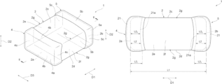
- FIG. 1 is a perspective view showing a multilayer conductor component according to an embodiment.
- FIG. 2 is a diagram for explaining a cross-sectional configuration of the multilayer conductor component of FIG. 1 .
- FIG. 3 is an exploded perspective view showing the configuration of the internal conductor.
- FIG. 4 is a bottom view showing the multilayer conductor component of FIG. 1 .
- FIG. 5 is a side surface view showing the multilayer conductor component of FIG. 1 .
- a multilayer conductor component 1 includes an element body 2 having a rectangular parallelepiped shape, and a pair of external electrodes 4 and 5 disposed on the surface of the element body 2 .
- the pair of external electrodes 4 and 5 are disposed at both ends of the element body 2 and are spaced from each other.
- the rectangular parallelepiped shape includes a rectangular parallelepiped shape in which corner portions and ridge portions are chamfered and a rectangular parallelepiped shape in which corner portions and ridge portions are rounded.
- the multilayer inductor component 1 can be applied to, for example, a bead inductor or a power inductor.
- the element body 2 has a rectangular parallelepiped shape.
- the element body 2 has, as its surface, a pair of end surfaces 2 a and 2 b , a pair of main surfaces 2 c and 2 d , and a pair of side surfaces 2 e and 2 f .
- the end surfaces 2 a and 2 b are opposed to each other.
- the main surfaces 2 c and 2 d are opposed to each other.
- the side surfaces 2 e and 2 f are opposed to each other.
- Each of the pair of end surfaces 2 a and 2 b is adjacent to each of the pair of main surfaces 2 c and 2 d and the pair of side surfaces 2 e and 2 f .
- the main surface 2 d constitutes a mounting surface.
- the mounting surface is defined as a surface facing other electronic devices when the multilayer conductor component 1 is mounted on the other electronic devices (for example, a circuit substrate or an electronic component), not shown.
- the direction in which the pair of end surfaces 2 a and 2 b opposed to each other is the length direction of the element body 2 .
- the direction in which the pair of main surfaces 2 c and 2 d opposed to each other is the height direction of the element body 2 .
- the direction in which the pair of side surfaces 2 e and 2 f opposed to each other is the width direction of the element body 2 .
- the first direction D 1 , the second direction D 2 , and the third direction D 3 are orthogonal to each other.
- a length L 1 (see FIGS. 4 and 5 ) of the element body 2 in the first direction D 1 is longer than the length of the element body 2 in the second direction D 2 and the length of the element body 2 in the third direction D 3 .
- the length of the element body 2 in the second direction D 2 is shorter than the length of the element body 2 in the third direction D 3 . That is, in this embodiment, the pair of end surfaces 2 a and 2 b , the pair of main surfaces 2 c and 2 d , and the pair of side surfaces 2 e and 2 f have rectangular shapes.
- the length L 1 of the element body 2 in the first direction D 1 is, for example, 2 mm.
- the length of the element body 2 in the second direction D 2 is, for example, 0.85 mm.
- the length of the element body 2 in the third direction D 3 is, for example, 1.6 mm.
- the length L 1 of the element body 2 in the first direction D 1 may be equal to the length of the element body 2 in the second direction D 2 and the length of the element body 2 in the third direction D 3 .
- the length of the element body 2 in the second direction D 2 and the length of the element body 2 in the third direction D 3 may be equal to each other.
- values including a slight difference within a preset range, a manufacturing error, or the like may be “equal”. For example, when a plurality of values is included in a range of ⁇ 5% of an average value of the plurality of values, the plurality of values is defined to be equal.
- the end surfaces 2 a and 2 b extend in the second direction D 2 in such a way to connect the pair of main surfaces 2 c and 2 d . That is, the end surfaces 2 a and 2 b extend in a direction intersecting the main surfaces 2 c and 2 d .
- the end surfaces 2 a and 2 b also extend in the third direction D 3 .
- the pair of main surfaces 2 c and 2 d extend in the first direction D 1 in such a way to connect the pair of end surfaces 2 a and 2 b .
- the pair of main surfaces 2 c and 2 d also extend in the third direction D 3 .
- the pair of side surfaces 2 e and 2 f extend in the second direction D 2 in such a way to connect the pair of main surfaces 2 c and 2 d .
- the pair of side surfaces 2 e and 2 f also extend in the first direction D 1 .
- the element body 2 includes four ridge portions 2 g extending along the first direction D 1 and eight ridge portions 2 h extending along the outer edges of the pair of end surfaces 2 a and 2 b .
- Each ridge portion 2 g is located between each of the pair of main surfaces 2 c and 2 d and each of the pair of side surfaces 2 e and 2 f adjacent to each other. That is, four ridge portions 2 g are located between the main surface 2 c and the side surface 2 e , between the side surface 2 e and the main surface 2 d , between the main surface 2 d and the side surface 2 f , and between the side surface 2 f and the main surface 2 c.
- the eight ridge portions 2 h are located between each of the pair of end surfaces 2 a and 2 b and each of the pair of main surfaces 2 c and 2 d and the pair of side surfaces 2 e and 2 f adjacent to each other. That is, eight ridge portions 2 h are located between the end surface 2 a and the main surface 2 c , between the end surface 2 a and the main surface 2 d , between the end surface 2 a and the side surface 2 e , between the end surface 2 a and the side surface 2 f , between the end surface 2 b and the main surface 2 c , between the end surface 2 b and the main surface 2 d , and between the end surface 2 b and the side surface 2 e , and between the end surface 2 b and the side surface 2 f.
- the ridge portions 2 g and 2 h are rounded in such a way that their surfaces are curved.
- the radii of curvature of the ridge portions 2 g and 2 h are, for example, 10% or more and 15% or less of the length of the element body 2 in the second direction D 2 .
- the radii of curvature of the ridge portions 2 g and 2 h are, for example, 90 ⁇ m.
- the radii of curvature of the ridge portions 2 g and 2 h may be different from each other.
- Sinterabilities of the ridge portions 2 g and 2 h are greater than sinterabilities of portions of the element body 2 other than the ridge portions 2 g and 2 h .
- the sinterabilities can be determined, for example, on the basis of a cross-sectional photograph of the element body 2 .
- the sinterabilities of the ridge portions 2 g and 2 h can be enhanced, for example, by performing barrel polishing on the green chips before firing when the element body 2 is manufactured.
- the ridge portion can be rounded in such a way that its surface is curved, the holes in the ridge portion can be reduced, and the density of the ridge portion can be increased compared to other portions of the green chip. As a result, the sinterabilities of the ridge portions 2 g and 2 h after firing can be improved.
- the element body 2 is formed by stacking a plurality of insulator layers 6 .
- the element body 2 includes a plurality of laminated insulator layers 6 .
- the plurality of insulator layers 6 are stacked in a direction in which the main surface 2 c and the main surface 2 d (See FIGS. 1 and 2 ) are opposed to each other. That is, the stacking direction of the plurality of insulator layers 6 coincides with the direction in which the main surface 2 c and the main surface 2 d are opposed to each other.
- the direction in which the main surface 2 c and the main surface 2 d are opposed to each other is also referred to as a “stacking direction”.
- Each insulator layer 6 has a substantially rectangular shape. In the actual element body 2 , the insulator layers 6 are integrated in such a way that boundaries between the layers 6 cannot be visually recognized.
- Each insulator layer 6 is formed of a sintered body of a ceramic green sheet containing a ferrite material (for example, a Ni—Cu—Zn-based ferrite material, a Ni—Cu—Zn—Mg-based ferrite material, or a Ni—Cu-based ferrite material). That is, the element body 2 is made of a ferrite sintered body.
- a ferrite material for example, a Ni—Cu—Zn-based ferrite material, a Ni—Cu—Zn—Mg-based ferrite material, or a Ni—Cu-based ferrite material.
- the multilayer inductor component 1 further includes, as internal conductors disposed inside the element body 2 , a plurality of coil conductors 16 a , 16 b , 16 c , 16 d , 16 e , and 16 f , a pair of connection conductors 17 , 18 and, and a plurality of through-hole conductors 19 a , 19 b , 19 c , 19 d , and 19 e .
- the coil conductors 16 a to 16 f constitute the coil 15 inside the element body 2 .
- the coil conductors 16 a to 16 f include a conductive material (for example, Ag or Pd).
- the coil conductors 16 a to 16 f are formed as sintered bodies of a conductive paste containing a conductive material (for example, Ag powder or Pd powder).
- connection conductor 17 is connected to the coil conductor 16 a .
- the connection conductor 17 is disposed on the end surface 2 b side of the element body 2 .
- the connection conductor 17 has an end portion 17 a exposed on the end surface 2 b .
- the end portion 17 a is exposed at a position closer to the main surface 2 c than the central portion of the end surface 2 b when viewed from the direction orthogonal to the end surface 2 b .
- the end portion 17 a is connected to the external electrode 5 . That is, the coil conductor 16 a is electrically connected to the external electrode 5 through the connection conductor 17 .
- the conductor pattern of the coil conductor 16 a and the conductor pattern of the connection conductor 17 are formed integrally and continuously.
- connection conductor 18 is connected to the coil conductor 16 f .
- the connection conductor 18 is disposed on the end surface 2 a side of the element body 2 .
- the connection conductor 18 has an end portion 18 a exposed on the end surface 2 a .
- the end portion 18 a is exposed at a position closer to the main surface 2 d than the central portion of the end surface 2 a when viewed from the direction orthogonal to the end surface 2 a .
- the end portion 18 a is connected to the external electrode 4 . That is, the coil conductor 16 f is electrically connected to the external electrode 4 through the connection conductor 18 .
- the conductor pattern of the coil conductor 16 f and the conductor pattern of the connection conductor 18 are formed integrally and continuously.
- the coil conductors 16 a to 16 f are arranged side by side in the lamination direction of the insulator layers 6 in the element body 2 .
- the coil conductors 16 a to 16 f are arranged in the order of the coil conductor 16 a , the coil conductor 16 b , the coil conductor 16 c , the coil conductor 16 d , the coil conductor 16 e , and the coil conductor 16 f from the side closer to the main surface 2 c.
- the through-hole conductors 19 a to 19 e connect ends of the coil conductors 16 a to 16 f to each other.
- the coil conductors 16 a to 16 f are electrically connected to each other by through-hole conductors 19 a to 19 e .
- the coil 15 is configured by electrically connecting a plurality of coil conductors 16 a to 16 f .
- Each of the through-hole conductors 19 a to 19 e contains a conductive material (for example, Ag or Pd).
- each of the through-hole conductors 19 a to 19 e is configured as a sintered body of a conductive paste containing a conductive material (for example, Ag powder or Pd powder).
- the through-hole conductors 19 a to 19 e are arranged side by side in the stacking direction of the insulator layers 6 in the element body 2 .
- the plurality of through-hole conductors 19 a to 19 e are arranged in the order of the through-hole conductor 19 a , the through-hole conductor 19 b , the through-hole conductor 19 c , the through-hole conductor 19 d , and the through-hole conductor 19 e from the side closer to the main surface 2 c.
- the external electrode 4 is located at an end portion on the end surface 2 a side of the element body 2 when viewed from the first direction D 1 .
- the external electrode 4 includes an electrode portion 4 a located on the end surface 2 a , electrode portions 4 b located on the main surfaces 2 c and 2 d , and electrode portions 4 c located on the side surfaces 2 e and 2 f . That is, the external electrode 4 is formed on the five surfaces 2 a , 2 c , 2 d , 2 e , and 2 f .
- the external electrode 4 is disposed over the end surface 2 a , the main surfaces 2 c and 2 d , and the side surfaces 2 e , and 2 f.
- the electrode portions 4 a , 4 b , and 4 c adjacent to each other are connected and electrically connected to each other at the ridge portions 2 g and 2 h of the element body 2 .
- the electrode portion 4 a and each of the electrode portions 4 b are connected at the ridge portion 2 h between the end surface 2 a and each of the main surfaces 2 c and 2 d .
- the electrode portion 4 a and each of the electrode portions 4 c are connected at the ridge portion 2 h between the end surface 2 a and each of the side surfaces 2 e and 2 f .
- Each of the electrode portion 4 b and each of the electrode portion 4 c are connected at the ridge portion 2 g between each of the main surfaces 2 c and 2 d and each of the side surfaces 2 e and 2 f.
- the electrode portion 4 a is disposed in such a way to entirely cover the end portion 18 a of the connection conductor 18 exposed at the end surface 2 a , and the connection conductor 18 is directly connected to the external electrode 4 . That is, the connection conductor 18 connects the coil conductor 16 a (one end of the coil 15 ) and the electrode portion 4 a . Thus, the coil 15 is electrically connected to the external electrode 4 .
- the external electrode 5 is located at an end portion on the end surface 2 b side of the element body 2 when viewed from the first direction D 1 .
- the external electrode 5 includes an electrode portion 5 a located on the end surface 2 b , an electrode portions 5 b located on the main surfaces 2 c and 2 d , and an electrode portions 5 c located on the side surfaces 2 e and 2 f . That is, the external electrodes 5 are formed on the five surfaces 2 b , 2 c , 2 d , 2 e , and 2 f .
- the external electrode 5 is disposed over the end surface 2 b , the main surfaces 2 c and 2 d , and the side surfaces 2 e and 2 f.
- the electrode portions 5 a , 5 b , and 5 c adjacent to each other are connected and electrically connected to each other at the ridge portions 2 g and 2 h of the element body 2 .
- the electrode portion 5 a and each of the electrode portions 5 b are connected at the ridge portion 2 h between the end surface 2 b and each of the main surfaces 2 c and 2 d .
- the electrode portion 5 a and each of the electrode portions 5 c are connected at the ridge portion 2 h between the end surface 2 b and each of the side surfaces 2 e and 2 f .
- Each of the electrode portion 5 b and each of the electrode portion 5 c are connected at the ridge portion 2 g between each of the main surfaces 2 c and 2 d and each of the side surfaces 2 e and 2 f.
- the electrode portion 5 a is disposed in such a way to entirely cover the end portion 17 a of the connection conductor 17 exposed at the end surface 2 b , and the connection conductor 17 is directly connected to the external electrode 5 . That is, the connection conductor 17 connects the coil conductor 16 f (the other end of the coil 15 ) and the electrode portion 5 a . Thus, the coil 15 is electrically connected to the external electrode 5 .
- Each of the external electrodes 4 and 5 includes a sintered metal layer 21 , a first plating layer 23 , and a second plating layer 25 . That is, the electrode portions 4 a , 4 b , and 4 c and the electrode portions 5 a , 5 b , and 5 c include the sintered metal layer 21 , the first plating layer 23 , and the second plating layer 25 , respectively.
- the second plating layer 25 constitutes the outermost layer of the external electrode 4 and 5 . None of the external electrode 4 and 5 includes a resin electrode layer containing resin.
- the sintered metal layer 21 is disposed on the surface of the element body 2 .
- the sintered metal layer 21 of the external electrode 4 is disposed over the pair of main surfaces 2 c and 2 d , the pair of side surfaces 2 e and 2 f , and the end surface 2 a .
- the sintered metal layer 21 of the external electrode 5 is disposed over the pair of main surfaces 2 c and 2 d , the pair of side surfaces 2 e and 2 f , and the end surface 2 b.
- the sintered metal layer 21 is formed by applying a conductive paste to the surface of the element body 2 and baking it.
- the conductive paste is applied to the surface of the element body 2 by, for example, a dipping method.
- a conductive paste for example, a mixture of a conductor component, a glass component, an organic binder, and an organic solvent is used.
- the conductor component is, for example, a metal powder such as Ag or Cu. In the present embodiment, the conductor component is Ag powder.
- the thickness of the portion disposed on the end surfaces 2 a and 2 b decreases toward the ridge portions 2 h and increases toward the central portions of the end surfaces 2 a and 2 b .
- the maximum thickness of the electrode portions 4 a and 5 a is, for example, 40 ⁇ m or more and 50 ⁇ m or more.
- the maximum thickness of the electrode portions 4 b and 5 b is, for example, 20 ⁇ m.
- the maximum thickness of the electrode portions 4 c and 5 c is, for example, 20 ⁇ m.
- the thicknesses of the electrode portions 4 a , 4 b and 4 c can be controlled by, for example, the thickness of the conductive paste applied to the element body 2 .
- FIG. 4 shows a plan view of the multilayer conductor component 1 as viewed from the main surface 2 d side.
- a plan view of the multilayer conductor component 1 as viewed from the main surface 2 c side is omitted since it is equivalent to the plan view of the multilayer conductor component 1 as viewed from the main surface 2 d side shown in FIG. 4 .
- FIG. 5 shows a plan view of the multilayer conductor component 1 as viewed from the side surface 2 f side.
- the plan view of the multilayer conductor component 1 as viewed from the side surface 2 e side is omitted since it is equivalent to the plan view of the multilayer conductor component 1 as viewed from the side surface 2 f side shown in FIG. 5 .
- each sintered metal layer 21 is continuous over the pair of main surfaces 2 c , 2 d , the pair of side surfaces 2 e , 2 f , and the four ridge portions 2 g in such a way as to surround the element body 2 .
- the edge 21 a has an entirely curved shape in such a way that the central portion of each of the pair of main surfaces 2 c and 2 d and the pair of side surfaces 2 e and 2 f is depressed toward a reference plane.
- the reference plane is defined as an imaginary plane including the end surface 2 a on which the external electrode 4 is provided, with respect to the edge 21 a of the external electrode 4 .
- the reference plane is defined as an imaginary plane including the end surface 2 b on which the external electrode 5 is provided, with respect to the edge 21 a of the external electrode 5 .
- the shape of the edge 21 a can be controlled, for example, by appropriately adjusting the constituent materials of the conductive paste applied to the surface of the element body 2 .
- the shape of the edge 21 a can also be controlled, for example, by applying a fluorine hydrophobic treatment to the surface of the element body 2 when applying the conductive paste.
- the distance from the edge 21 a to the reference plane in the first direction D 1 is defined as an electrode length L 2 .
- the edge 21 a is continuous over the pair of main surfaces 2 c and 2 d , the pair of side surfaces 2 e and 2 f , and the four ridge portions 2 g while varying the electrode length L 2 .
- the electrode length L 2 is 5% or more and 15% or less of the length L 1 of the element body 2 in the first direction D 1 .
- the electrode length L 2 varies in a range of 5% or more and 15% or less of the length L 1 of the element body 2 in the first direction D 1 .
- the electrodes length L 2 1 in the four ridge portions 2 g are equivalent to each other.
- the electrode length L 2 2 at the central portion of the main surface 2 d in the third direction D 3 is shorter than the electrode lengths L 2 1 at the ridge portions 2 g located on both sides of the main surface 2 d in the third direction D 3 .
- the electrode length L 2 monotonically increases from the central portion of the main surface 2 d in the third direction D 3 toward the ridge portions 2 g located on both sides of the main surface 2 d in the third direction D 3 .
- the term “monotonic increase” means that there is no tendency to decrease and means a broad monotonic increase.
- the electrode length L 2 changes with the electrode length L 2 2 as the minimum value and the electrode lengths L 2 1 as the maximum value. It can also be said that the edge 21 a does not have an inflection point between the central portion of the main surface 2 d in the third direction D 3 and the ridge portions 2 g.
- the electrode length at the central portion of the main surface 2 c in the third direction D 3 is shorter than the electrode lengths L 2 1 at the ridge portions 2 g located on both sides of the main surface 2 c in the third direction D 3 .
- the electrode length at the central portion of the main surface 2 c in the third direction D 3 is equal to the electrode length L 2 2 .
- the electrode length L 2 monotonically increases from the central portion of the main surface 2 c in the third direction D 3 toward the ridge portions 2 g located on both sides of the main surface 2 c in the third direction D 3 .
- the electrode length L 2 changes with the electrode length L 2 2 as the minimum value and the electrode lengths
- edge 21 a does not have an inflection point between the central portion of the main surface 2 c in the third direction D 3 and the ridge portions 2 g.
- the electrode length L 2 3 at the central portion of the side surface 2 f in the second direction D 2 is shorter than the electrode lengths L 2 1 at the ridge portions 2 g located on both sides of the side surface 2 f in the second direction D 2 .
- the electrode length L 2 3 is longer than the electrode length L 2 2 .
- the electrode length L 2 monotonically increases from the central portion of the side surface 2 f in the second direction D 2 toward the ridge portions 2 g located on both sides of the side surface 2 f in the second direction D 2 .
- the electrode length L 2 changes with the electrode length L 2 3 as the minimum value and the electrode length L 2 1 as the maximum value. It can also be said that the edge 21 a does not have an inflection point from the central portion of the side surface 2 f in the second direction D 2 to the ridge portions 2 g.
- the electrode length at the central portion of the side surface 2 e in the second direction D 2 is shorter than the electrode lengths L 2 1 at the ridge portions 2 g located on both sides of the side surface 2 e in the second direction D 2 .
- the electrode length at the central portion of the side surface 2 e in the second direction D 2 is equal to the electrode length L 2 2 .
- the electrode length L 2 monotonically increases from the central portion of the side surface 2 e in the second direction D 2 toward the ridge portions 2 g located on both sides of the side surface 2 e in the second direction D 2 . 2 2 .
- the electrode length L 2 changes with the electrode length L 2 3 as the minimum value and the electrode length L 2 1 as the maximum value. It can also be said that the edge 21 a does not have an inflection point from the central portion of the side surface 2 e in the second direction D 2 to the ridge portions 2 g.
- the first plating layer 23 covers the sintered metal layer 21 .
- the first plating layer 23 covers the sintered metal layer 21 with a substantially uniform thickness.
- the thickness of the first plating layer 23 is, for example, 0.5 ⁇ m or more and 6.5 ⁇ m or less.
- the first plating layer 23 is formed on the sintered metal layer 21 by plating method.
- the first plating layer 23 is, for example, an Ni plating layer and includes Ni.
- the second plating layer 25 covers the first plating layer 23 .
- the second plating layer 25 covers the first plating layer 23 with a substantially uniform thickness.
- the thickness of the second plating layer 25 is, for example, 1.5 ⁇ m or more and 8.0 ⁇ m or less.
- the second plating layer 25 is formed on the first plating layer 23 by plating method.
- the second plating layer 25 is, for example, an Sn plating layer and includes Sn.
- the multilayer conductor component 1 may further include a third plating layer (not shown) overlying the second plating layer 25 .
- the first plating layer 23 may be a Cu plating layer
- the second plating layer 25 may be a Ni plating layer
- the third plating layer may be a Sn plating layer.
- the edge 21 a of the sintered metal layer 21 is continuous over the pair of side surfaces 2 e and 2 f , the pair of main surfaces 2 c and 2 d , and the ridge portions 2 g .
- the stress due to thermal shock or the like is likely to be concentrated in a portion of the edge 21 a where the electrode length L 2 is long.
- the stress tends to concentrate on the edge 21 a via the solder.
- the electrode length L 2 2 at the central portion of the main surface 2 d in the third direction D 3 is shorter than the electrode length L 2 1 at each ridge portion 2 g located on both sides of the main surface 2 d in the third direction D 3 . Therefore, in the multilayer conductor component 1 , the stress can be dispersed from the central portion of the main surface 2 d to the ridge portions 2 g located on both sides of the main surface 2 d .
- the electrode length L 2 3 at the central portion of each of the pair of side surfaces 2 e and 2 f in the second direction D 2 is shorter than the electrode length L 2 1 at each of the ridge portions 2 g located on both sides of each of the pair of side surfaces 2 e and 2 f in the second direction D 2 . Therefore, the stress can be dispersed from the central portion of each of the pair of side surfaces 2 e and 2 f to each of the ridge portions 2 g located on both sides of each of the pair of side surfaces 2 e and 2 f . From the above, the occurrence of cracks in the element body 2 can be suppressed.
- the electrode length L 2 monotonically increases from the central portion of the main surface 2 d in the third direction D 3 toward each of the ridge portion 2 g located on both sides of the main surface 2 d in the third direction D 3 . If the edge 21 a has an inflection point between the central portion of the main surface 2 d in the third direction D 3 and the ridge portion 2 g , and a part of the edge 21 a protrudes or is depressed in the first direction D 1 , stress may be concentrated in the part or the vicinity thereof.
- the multilayer conductor component 1 can suppress such stress concentration. Therefore, the stress can be reliably dispersed from the central portion of the main surface 2 d to each of the ridge portions 2 g located on both sides of the main surface 2 d.
- the electrode length L 2 monotonically increases from the central portion of each of side surfaces 2 e and 2 f in the second direction D 2 toward each of the ridge portions 2 g located on both sides of each of side surfaces 2 e and 2 f in the second direction D 2 . If the edge 21 a has an inflection point between the central portion of each of the side surfaces 2 e and 2 f in the second direction D 2 and the ridge portions 2 g , and a part of the edge 21 a protrudes or is depressed in the first direction D 1 , stress may be concentrated in the part or the vicinity thereof.
- the multilayer conductor component 1 can suppress such stress concentration. Therefore, the stress can be reliably dispersed from the central portion of each of the side surfaces 2 e and 2 f to each of the ridge portions 2 g located on both sides of each of the side surfaces 2 e and 2 f.
- the sinterabilities of the ridge portions 2 g are greater than the sinterabilities of the other portions of the element body 2 . As a result, the strengths of the ridge portions 2 g are improved, and the occurrence of cracks in the element body 2 is further suppressed.
- the element body 2 includes the sintered ferrite body.
- the firing temperature of the dielectric ceramic or the like is about 1000° C., while the firing temperature of the ferrite is about 900° C.
- the element body 2 since the element body 2 includes the ferrite sintered body having a low firing temperature and having difficulty in improving the strength, it is more important to suppress the occurrence of cracks.
- the electrode length L 2 is 5% or more and 15% or less of the length L 1 of the element body 2 in the first direction D 1 .
- the electrode length L 2 is 5% or more, the mounting strength of the multilayer conductor component 1 can be increased.
- the electrode length L 2 is 15% or less, the main surfaces 2 c and 2 d and the side surfaces 2 e and 2 f are prevented from being pulled via the solder starting from the central portion side in the first direction D 1 . Thus, the stress applied to the element body 2 can be suppressed.
- the electrode length at the central portion of the main surface 2 c in the third direction D 3 is shorter than the electrode length L 2 1 at each of the ridge portions 2 g located on both sides of the main surface 2 c in the third direction D 3 . Therefore, the stress can be dispersed from the central portion of the main surface 2 c to the ridge portions 2 g located on both sides of the main surface 2 c .
- the amount of solder provided on the main surface 2 c is smaller than the amount of solder provided on the main surface 2 d or the pair of side surfaces 2 e and 2 f , stress may be concentrated on the edge 21 a via the solder on the main surface 2 c .
- the occurrence of cracks in the element body 2 is further suppressed by dispersing the stress in the ridge portions 2 g.
- the electrode length L 2 monotonically increases from the central portion of the main surface 2 c in the third direction D 3 toward the ridge portions 2 g located on both sides of the main surface 2 c in the third direction D 3 . If the edge 21 a has an inflection point between the central portion of the main surface 2 c in the third direction D 3 and the ridge portion 2 g , and a part of the edge 21 a protrudes or is depressed in the first direction D 1 , stress may be concentrated in the part or the vicinity thereof.
- the multilayer conductor component 1 can suppress such stress concentration. Therefore, the stress can be reliably dispersed from the main surface 2 c to the ridge portions 2 g located on both sides of the main surface 2 c.
- Each ridge portion 2 g is rounded in such a way that its surface is curved. If a corner exists in the ridge portion 2 g , stress may be concentrated in the corner. The rounded ridge portion 2 g suppresses concentration of stress. As a result, the occurrence of cracks in the element body 2 is further suppressed.
- both the electrode length L 2 2 and the electrode length L 2 3 are shorter than the electrode length L 2 1 , but one of the electrode length L 2 2 and the electrode length L 2 3 may be shorter than the electrode length L 2 1 and the other may be equal to or less than the electrode length L 2 1 .
- the electrode length L 2 2 is shorter than the electrode length L 2 1 and the electrode length L 2 3 is equal to or less than the electrode length L 2 1 , it is possible to suppress the concentration of the stress at the central portions of the side surfaces 2 e and 2 f while dispersing the stress from the central portion of the main surface 2 d to the ridge portions 2 g located on both sides of the main surface 2 d .
- the electrode length L 2 2 is equal to or less than the electrode length L 2 1 , it is possible to suppress the concentration of the stress at the central portion of the main surface 2 d while dispersing the stress from the central portions of the side surfaces 2 e and 2 f to the ridge portions 2 g located on both sides of the side surfaces 2 e and 2 f.
- the electrodes length L 2 1 at the four ridge portions 2 g may be different from each other. Even in this case, if the electrode length L 2 2 is shorter than the electrode length L 2 1 , the stress can be dispersed from the central portion of the main surface 2 d to the ridge portions 2 g located on both sides of the main surface 2 d . If the electrode length L 2 3 is shorter than the electrode length L 2 1 , the stress can be dispersed from the central portion of each of the side surfaces 2 e and 2 f to the ridge portions 2 g located on both sides of each of the side surfaces 2 e and 2 f.
- the external electrodes 4 and 5 have the same shape, but the external electrodes 4 and 5 may have different shapes.
- the electrode length L 2 2 may be shorter than the electrode length L 2 1
- the electrode length L 2 3 may be the electrode length L 2 1 or less.
- the electrode length L 2 2 may be the electrode length L 2 1 or less
- the electrode length L 2 3 may be shorter than the electrode length L 2 1 . In this case, it is possible to suppress the cracks of the element body 2 caused by at least one of the external electrodes 4 and 5 .
- the multilayer conductor component 1 may have a linear conductor instead of the coil conductors 16 a to 16 f as the internal conductor.
Landscapes
- Engineering & Computer Science (AREA)
- Power Engineering (AREA)
- Microelectronics & Electronic Packaging (AREA)
- Manufacturing & Machinery (AREA)
- Coils Or Transformers For Communication (AREA)
Abstract
Description
Claims (19)
Applications Claiming Priority (2)
| Application Number | Priority Date | Filing Date | Title |
|---|---|---|---|
| JP2020-098412 | 2020-06-05 | ||
| JP2020098412A JP2021192404A (en) | 2020-06-05 | 2020-06-05 | Multilayer inductor component |
Publications (2)
| Publication Number | Publication Date |
|---|---|
| US20210383960A1 US20210383960A1 (en) | 2021-12-09 |
| US12125627B2 true US12125627B2 (en) | 2024-10-22 |
Family
ID=78787138
Family Applications (1)
| Application Number | Title | Priority Date | Filing Date |
|---|---|---|---|
| US17/337,985 Active 2043-05-19 US12125627B2 (en) | 2020-06-05 | 2021-06-03 | Multilayer inductor component |
Country Status (3)
| Country | Link |
|---|---|
| US (1) | US12125627B2 (en) |
| JP (1) | JP2021192404A (en) |
| CN (1) | CN113764154A (en) |
Families Citing this family (2)
| Publication number | Priority date | Publication date | Assignee | Title |
|---|---|---|---|---|
| JP7545295B2 (en) * | 2020-11-02 | 2024-09-04 | Tdk株式会社 | Multilayer coil component and mounting structure of multilayer coil component |
| JP2023120050A (en) * | 2022-02-17 | 2023-08-29 | 太陽誘電株式会社 | Coil component, circuit board, electronic device, and method for manufacturing coil component |
Citations (15)
| Publication number | Priority date | Publication date | Assignee | Title |
|---|---|---|---|---|
| JPH03229407A (en) | 1990-02-03 | 1991-10-11 | Taiyo Yuden Co Ltd | Laminated electronic component and manufacture thereof |
| JP2000331832A (en) | 1999-05-18 | 2000-11-30 | Tokin Corp | Laminate type impedance element |
| US20030169556A1 (en) | 2002-03-07 | 2003-09-11 | Tdk Corporation | Ceramic electronic device, paste coating method, and paste coating apparatus |
| JP2006310700A (en) | 2005-05-02 | 2006-11-09 | Tdk Corp | Electronic components |
| US20110287176A1 (en) | 2010-05-19 | 2011-11-24 | Murata Manufacturing Co., Ltd. | Method for producing ceramic electronic component |
| US20140192453A1 (en) * | 2013-01-09 | 2014-07-10 | Samsung Electro-Mechanics Co., Ltd. | Conductive resin composition, multilayer ceramic capacitor having the same, and method of manufacturing the multilayer ceramic capacitor |
| JP2015053495A (en) | 2014-10-07 | 2015-03-19 | 株式会社村田製作所 | Ceramic electronic component and method for manufacturing the same |
| JP2016115918A (en) | 2014-12-11 | 2016-06-23 | 株式会社村田製作所 | Laminated ceramic electronic component |
| US20170345553A1 (en) * | 2016-05-30 | 2017-11-30 | Tdk Corporation | Multilayer coil component |
| US20180033540A1 (en) * | 2016-07-26 | 2018-02-01 | Samsung Electro-Mechanics Co., Ltd. | Coil component and method of manufacturing the same |
| US20180137964A1 (en) | 2016-11-16 | 2018-05-17 | Tdk Corporation | Electronic component |
| JP2018125455A (en) | 2017-02-02 | 2018-08-09 | Tdk株式会社 | Laminate coil component |
| US20180374628A1 (en) | 2017-06-26 | 2018-12-27 | Murata Manufacturing Co., Ltd. | Multilayer inductor |
| US20190148075A1 (en) * | 2017-11-14 | 2019-05-16 | Taiyo Yuden Co., Ltd. | Ceramic electronic device and manufacturing method of ceramic electronic device |
| US20200118755A1 (en) | 2018-10-12 | 2020-04-16 | Taiyo Yuden Co., Ltd. | Ceramic electronic component, ceramic electronic component manufacturing method, and ceramic electronic component-mounting circuit board |
Family Cites Families (8)
| Publication number | Priority date | Publication date | Assignee | Title |
|---|---|---|---|---|
| JPH0669062A (en) * | 1992-08-12 | 1994-03-11 | Murata Mfg Co Ltd | Laminated capacitor |
| JP2007305830A (en) * | 2006-05-12 | 2007-11-22 | Murata Mfg Co Ltd | Method for manufacturig electronic component, electronic component, and electronic equipment |
| JP4479747B2 (en) * | 2007-05-30 | 2010-06-09 | Tdk株式会社 | Multilayer capacitor |
| JP4849123B2 (en) * | 2008-12-22 | 2012-01-11 | Tdk株式会社 | Manufacturing method of multilayer capacitor |
| JP6809865B2 (en) * | 2016-10-17 | 2021-01-06 | 太陽誘電株式会社 | Ceramic electronic components and their manufacturing methods |
| JP6575537B2 (en) * | 2017-01-10 | 2019-09-18 | 株式会社村田製作所 | Inductor parts |
| JP6708162B2 (en) * | 2017-04-25 | 2020-06-10 | 株式会社村田製作所 | Inductor |
| JP6946876B2 (en) * | 2017-09-08 | 2021-10-13 | Tdk株式会社 | Electronic components and electronic component equipment |
-
2020
- 2020-06-05 JP JP2020098412A patent/JP2021192404A/en active Pending
-
2021
- 2021-05-18 CN CN202110550777.5A patent/CN113764154A/en active Pending
- 2021-06-03 US US17/337,985 patent/US12125627B2/en active Active
Patent Citations (31)
| Publication number | Priority date | Publication date | Assignee | Title |
|---|---|---|---|---|
| JPH03229407A (en) | 1990-02-03 | 1991-10-11 | Taiyo Yuden Co Ltd | Laminated electronic component and manufacture thereof |
| JP2000331832A (en) | 1999-05-18 | 2000-11-30 | Tokin Corp | Laminate type impedance element |
| US20030169556A1 (en) | 2002-03-07 | 2003-09-11 | Tdk Corporation | Ceramic electronic device, paste coating method, and paste coating apparatus |
| JP2003264117A (en) | 2002-03-07 | 2003-09-19 | Tdk Corp | Ceramic electronic component, paste coating method and paster coater |
| US20040208987A1 (en) | 2002-03-07 | 2004-10-21 | Tdk Corporation | Ceramic electronic device, paste coating method, and paste coating apparatus |
| US20070000439A1 (en) | 2002-03-07 | 2007-01-04 | Tdk Corporation | Paste coating method |
| JP2006310700A (en) | 2005-05-02 | 2006-11-09 | Tdk Corp | Electronic components |
| US20110287176A1 (en) | 2010-05-19 | 2011-11-24 | Murata Manufacturing Co., Ltd. | Method for producing ceramic electronic component |
| JP2012004544A (en) | 2010-05-19 | 2012-01-05 | Murata Mfg Co Ltd | Method of manufacturing ceramic electronic component |
| US20130141836A1 (en) | 2010-05-19 | 2013-06-06 | Murata Manufacturing Co., Ltd. | Method for producing ceramic electronic component |
| US20140192453A1 (en) * | 2013-01-09 | 2014-07-10 | Samsung Electro-Mechanics Co., Ltd. | Conductive resin composition, multilayer ceramic capacitor having the same, and method of manufacturing the multilayer ceramic capacitor |
| US20170186549A1 (en) | 2014-10-07 | 2017-06-29 | Murata Manufacturing Co., Ltd. | Ceramic electronic component |
| US20160099106A1 (en) | 2014-10-07 | 2016-04-07 | Murata Manufacturing Co., Ltd. | Ceramic electronic component |
| JP2015053495A (en) | 2014-10-07 | 2015-03-19 | 株式会社村田製作所 | Ceramic electronic component and method for manufacturing the same |
| US20170186550A1 (en) | 2014-10-07 | 2017-06-29 | Murata Manufacturing Co., Ltd. | Ceramic electronic component |
| US20170263382A1 (en) | 2014-10-07 | 2017-09-14 | Murata Manufacturing Co., Ltd. | Ceramic electronic component |
| US20170287644A1 (en) | 2014-10-07 | 2017-10-05 | Murata Manufacturing Co., Ltd. | Ceramic electronic component |
| US20170365413A1 (en) | 2014-10-07 | 2017-12-21 | Murata Manufacturing Co., Ltd. | Ceramic electronic component |
| JP2016115918A (en) | 2014-12-11 | 2016-06-23 | 株式会社村田製作所 | Laminated ceramic electronic component |
| US20170345553A1 (en) * | 2016-05-30 | 2017-11-30 | Tdk Corporation | Multilayer coil component |
| US20180033540A1 (en) * | 2016-07-26 | 2018-02-01 | Samsung Electro-Mechanics Co., Ltd. | Coil component and method of manufacturing the same |
| US20180137964A1 (en) | 2016-11-16 | 2018-05-17 | Tdk Corporation | Electronic component |
| JP2018082039A (en) | 2016-11-16 | 2018-05-24 | Tdk株式会社 | Electronic components |
| JP2018125455A (en) | 2017-02-02 | 2018-08-09 | Tdk株式会社 | Laminate coil component |
| US20180374628A1 (en) | 2017-06-26 | 2018-12-27 | Murata Manufacturing Co., Ltd. | Multilayer inductor |
| JP2019009299A (en) | 2017-06-26 | 2019-01-17 | 株式会社村田製作所 | Multilayer inductor |
| US20190148075A1 (en) * | 2017-11-14 | 2019-05-16 | Taiyo Yuden Co., Ltd. | Ceramic electronic device and manufacturing method of ceramic electronic device |
| CN109786106A (en) | 2017-11-14 | 2019-05-21 | 太阳诱电株式会社 | The manufacturing method of ceramic electronic component and ceramic electronic component |
| US20220122775A1 (en) | 2017-11-14 | 2022-04-21 | Taiyo Yuden Co., Ltd. | Ceramic electronic device and manufacturing method of ceramic electronic device |
| US20200118755A1 (en) | 2018-10-12 | 2020-04-16 | Taiyo Yuden Co., Ltd. | Ceramic electronic component, ceramic electronic component manufacturing method, and ceramic electronic component-mounting circuit board |
| CN111048311A (en) | 2018-10-12 | 2020-04-21 | 太阳诱电株式会社 | Ceramic electronic component, method for manufacturing the same, and ceramic electronic component mounting circuit board |
Also Published As
| Publication number | Publication date |
|---|---|
| JP2021192404A (en) | 2021-12-16 |
| US20210383960A1 (en) | 2021-12-09 |
| CN113764154A (en) | 2021-12-07 |
Similar Documents
| Publication | Publication Date | Title |
|---|---|---|
| US11817263B2 (en) | Electronic component, circuit board, and method of mounting electronic component on circuit board | |
| US7106161B2 (en) | Coil component | |
| US11217391B2 (en) | Electronic component | |
| US11152154B2 (en) | Electronic component | |
| US10614946B2 (en) | Electronic component | |
| US11189413B2 (en) | Multilayer coil component and method for producing the same | |
| US11264171B2 (en) | Electronic component | |
| US12249467B2 (en) | Electronic component | |
| US10650972B2 (en) | Electronic component | |
| CN113393997B (en) | Laminated coil component | |
| US12125627B2 (en) | Multilayer inductor component | |
| US12094642B2 (en) | Multilayer inductor component | |
| US11289271B2 (en) | Electronic component | |
| JP2025072622A (en) | Multilayer coil parts | |
| US12525381B2 (en) | Multilayer coil component | |
| US12488936B2 (en) | Multilayer coil component | |
| US11551846B2 (en) | Multilayer coil component | |
| US20240258036A1 (en) | Electronic component and electronic component device | |
| US20250029784A1 (en) | Multilayer ceramic electronic component | |
| US20240120142A1 (en) | Electronic component | |
| US20240242861A1 (en) | Electronic component and chip varistor | |
| US20240212942A1 (en) | Electronic component |
Legal Events
| Date | Code | Title | Description |
|---|---|---|---|
| FEPP | Fee payment procedure |
Free format text: ENTITY STATUS SET TO UNDISCOUNTED (ORIGINAL EVENT CODE: BIG.); ENTITY STATUS OF PATENT OWNER: LARGE ENTITY |
|
| AS | Assignment |
Owner name: TDK CORPORATION, JAPAN Free format text: ASSIGNMENT OF ASSIGNORS INTEREST;ASSIGNORS:KATO, DAIKI;SHIMOYASU, MASASHI;TOZAWA, YOJI;AND OTHERS;REEL/FRAME:057023/0195 Effective date: 20210617 |
|
| STPP | Information on status: patent application and granting procedure in general |
Free format text: DOCKETED NEW CASE - READY FOR EXAMINATION |
|
| STPP | Information on status: patent application and granting procedure in general |
Free format text: NON FINAL ACTION MAILED |
|
| STPP | Information on status: patent application and granting procedure in general |
Free format text: RESPONSE TO NON-FINAL OFFICE ACTION ENTERED AND FORWARDED TO EXAMINER |
|
| STPP | Information on status: patent application and granting procedure in general |
Free format text: NOTICE OF ALLOWANCE MAILED -- APPLICATION RECEIVED IN OFFICE OF PUBLICATIONS |
|
| ZAAB | Notice of allowance mailed |
Free format text: ORIGINAL CODE: MN/=. |
|
| STPP | Information on status: patent application and granting procedure in general |
Free format text: AWAITING TC RESP., ISSUE FEE NOT PAID |
|
| STPP | Information on status: patent application and granting procedure in general |
Free format text: NOTICE OF ALLOWANCE MAILED -- APPLICATION RECEIVED IN OFFICE OF PUBLICATIONS |
|
| STPP | Information on status: patent application and granting procedure in general |
Free format text: PUBLICATIONS -- ISSUE FEE PAYMENT VERIFIED |
|
| STCF | Information on status: patent grant |
Free format text: PATENTED CASE |