US12117572B2 - Radiography apparatus - Google Patents
Radiography apparatus Download PDFInfo
- Publication number
- US12117572B2 US12117572B2 US17/412,758 US202117412758A US12117572B2 US 12117572 B2 US12117572 B2 US 12117572B2 US 202117412758 A US202117412758 A US 202117412758A US 12117572 B2 US12117572 B2 US 12117572B2
- Authority
- US
- United States
- Prior art keywords
- blocks
- radiation detector
- signal processing
- radiography apparatus
- block
- Prior art date
- Legal status (The legal status is an assumption and is not a legal conclusion. Google has not performed a legal analysis and makes no representation as to the accuracy of the status listed.)
- Active, expires
Links
- 238000002601 radiography Methods 0.000 title claims abstract description 56
- 239000000758 substrate Substances 0.000 claims abstract description 41
- 238000006243 chemical reaction Methods 0.000 claims abstract description 19
- 238000003384 imaging method Methods 0.000 abstract description 20
- 230000005855 radiation Effects 0.000 description 135
- 238000005516 engineering process Methods 0.000 description 31
- 238000000926 separation method Methods 0.000 description 24
- 239000000463 material Substances 0.000 description 11
- 238000009659 non-destructive testing Methods 0.000 description 9
- 238000004891 communication Methods 0.000 description 6
- 238000010586 diagram Methods 0.000 description 6
- 230000003321 amplification Effects 0.000 description 4
- 238000003199 nucleic acid amplification method Methods 0.000 description 4
- 238000005192 partition Methods 0.000 description 4
- 239000011347 resin Substances 0.000 description 4
- 229920005989 resin Polymers 0.000 description 4
- 229920002379 silicone rubber Polymers 0.000 description 4
- 239000004945 silicone rubber Substances 0.000 description 4
- 239000004642 Polyimide Substances 0.000 description 2
- 239000011159 matrix material Substances 0.000 description 2
- 229920001721 polyimide Polymers 0.000 description 2
- 238000012360 testing method Methods 0.000 description 2
- BQCADISMDOOEFD-UHFFFAOYSA-N Silver Chemical compound [Ag] BQCADISMDOOEFD-UHFFFAOYSA-N 0.000 description 1
- MCVAAHQLXUXWLC-UHFFFAOYSA-N [O-2].[O-2].[S-2].[Gd+3].[Gd+3] Chemical compound [O-2].[O-2].[S-2].[Gd+3].[Gd+3] MCVAAHQLXUXWLC-UHFFFAOYSA-N 0.000 description 1
- 229910021417 amorphous silicon Inorganic materials 0.000 description 1
- 230000005540 biological transmission Effects 0.000 description 1
- 239000000470 constituent Substances 0.000 description 1
- 238000001514 detection method Methods 0.000 description 1
- 239000010419 fine particle Substances 0.000 description 1
- 239000004033 plastic Substances 0.000 description 1
- 239000000843 powder Substances 0.000 description 1
- 229910052709 silver Inorganic materials 0.000 description 1
- 239000004332 silver Substances 0.000 description 1
- 239000010409 thin film Substances 0.000 description 1
- 238000002834 transmittance Methods 0.000 description 1
- 238000004804 winding Methods 0.000 description 1
Images


Classifications
-
- G—PHYSICS
- G01—MEASURING; TESTING
- G01T—MEASUREMENT OF NUCLEAR OR X-RADIATION
- G01T1/00—Measuring X-radiation, gamma radiation, corpuscular radiation, or cosmic radiation
- G01T1/16—Measuring radiation intensity
- G01T1/20—Measuring radiation intensity with scintillation detectors
- G01T1/2018—Scintillation-photodiode combinations
- G01T1/20182—Modular detectors, e.g. tiled scintillators or tiled photodiodes
-
- G—PHYSICS
- G01—MEASURING; TESTING
- G01T—MEASUREMENT OF NUCLEAR OR X-RADIATION
- G01T1/00—Measuring X-radiation, gamma radiation, corpuscular radiation, or cosmic radiation
- G01T1/16—Measuring radiation intensity
- G01T1/20—Measuring radiation intensity with scintillation detectors
- G01T1/208—Circuits specially adapted for scintillation detectors, e.g. for the photo-multiplier section
-
- G—PHYSICS
- G01—MEASURING; TESTING
- G01T—MEASUREMENT OF NUCLEAR OR X-RADIATION
- G01T1/00—Measuring X-radiation, gamma radiation, corpuscular radiation, or cosmic radiation
- G01T1/16—Measuring radiation intensity
- G01T1/20—Measuring radiation intensity with scintillation detectors
- G01T1/2002—Optical details, e.g. reflecting or diffusing layers
-
- G—PHYSICS
- G01—MEASURING; TESTING
- G01T—MEASUREMENT OF NUCLEAR OR X-RADIATION
- G01T1/00—Measuring X-radiation, gamma radiation, corpuscular radiation, or cosmic radiation
- G01T1/16—Measuring radiation intensity
- G01T1/20—Measuring radiation intensity with scintillation detectors
- G01T1/2018—Scintillation-photodiode combinations
- G01T1/20184—Detector read-out circuitry, e.g. for clearing of traps, compensating for traps or compensating for direct hits
Definitions
- the disclosed technology relates to a radiography apparatus.
- Non-destructive testing using radiation has been conventionally performed.
- JP2014-102202A discloses that a fluoroscopic image generated from an imaging plate as a radiation detection medium is acquired by emitting radiation from radiation source while the imaging plate is disposed on an outer periphery of a welded portion of a pipe to be tested and a radiation source is disposed on a central axis of the pipe.
- WO2016/017305A discloses a radiation measuring device in which a pixel array unit is logically divided into regions of 1 mm square corresponding to a scintillator divided into a plurality of partitions, and scintillation light generated by the scintillator is selectively emitted to the corresponding partition in the pixel array unit.
- an imaging plate In non-destructive testing of a pipe welded portion using radiation, an imaging plate is used as disclosed in JP2014-102202A.
- In order to display a latent image recorded on the imaging plate as an image it is necessary to irradiate a surface of the imaging plate exposed by radiation with a laser beam and measure light emission according to an exposure amount of the radiation. Therefore, in the non-destructive testing using the imaging plate, it is difficult to immediately display an image. That is, in the non-destructive testing using the imaging plate, it is difficult to acquire a test result at a site and immediately take measures according to the test result at the site.
- a digital detector array comprising a scintillator and a photoelectric conversion element
- a flexible DDA that can be wound around a surface of a pipe such as an imaging plate has not yet been put into practical use.
- the shape and size of the DDA are defined by the standard, and the shape and size are not suitable for use by winding the DDA around the surface of the pipe. In the non-destructive testing of the pipe welded portion, the optimum shape and size of the DDA change depending on, for example, the diameter and shape of the pipe.
- an object of the present invention is to provide a radiography apparatus capable of changing the shape and size at an imaging site.
- a radiography apparatus comprises a scintillator, and a substrate that is laminated on the scintillator and has a plurality of photoelectric conversion elements converting light emitted from the scintillator into electric charges, in which a laminate including the scintillator and the substrate is partitioned into a plurality of blocks, and the blocks are separable from each other.
- the shape and size of the laminate can be changed at an imaging site.
- Each of the plurality of blocks may have a connector provided in a boundary portion with another block. As a result, it is possible to reconnect the separated blocks.
- the laminate including the scintillator and the substrate may have flexibility. As a result, since the laminate can be curved, the radiography apparatus can be used for non-destructive testing of a welded portion of a pipe.
- the radiography apparatus may further comprise a plurality of switching elements provided on the substrate and provided corresponding to the plurality of photoelectric conversion elements, a plurality of gate lines provided on the substrate and transmitting drive signals for driving each of the plurality of switching elements, a plurality of signal lines provided on the substrate and transmitting electric signals based on the electric charges generated by the plurality of photoelectric conversion elements, a plurality of drive circuits connected to a part of different gate lines among the plurality of gate lines and outputting the drive signals, respectively, and a plurality of signal processing circuits connected to a part of different signal lines among the plurality of signal lines and processing the electric signals, respectively.
- each of the gate lines included in the block is connected to one of the plurality of drive circuits, and each of the signal lines included in the block is connected to one of the plurality of signal processing circuits.
- the plurality of drive circuits and the plurality of signal processing circuits are provided along one side of the laminate. As a result, it is possible to suppress the complication of leading of wiring connected to the drive circuit and the signal processing circuit.
- the plurality of drive circuits and the plurality of signal processing circuits may be provided along two sides of the laminate opposite to each other. In this case, the plurality of drive circuits are electrically connected to each other, and the plurality of signal processing circuits are electrically connected to each other.
- a radiography apparatus capable of changing the shape and size at an imaging site.
- FIG. 1 is a plan view showing an example of a configuration of a radiography apparatus according to an embodiment of the disclosed technology.
- FIG. 2 is a cross-sectional view taken along line 2 - 2 in FIG. 1 .
- FIG. 3 is a diagram showing an example of an electric configuration of the radiography apparatus according to the embodiment of the disclosed technology.
- FIG. 4 is a diagram showing an example of a configuration of a plurality of pixels constituting a radiation detector according to the embodiment of the disclosed technology.
- FIG. 5 A is a diagram showing an example of a configuration of a connector that connects blocks of the radiation detector according to the embodiment of the disclosed technology to each other.
- FIG. 5 B is a diagram showing an example of the configuration of the connector that connects the blocks of the radiation detector according to the embodiment of the disclosed technology to each other.
- FIG. 6 A is a plan view illustrating an aspect of separation of blocks of the radiation detector according to the embodiment of the disclosed technology.
- FIG. 6 B is a plan view illustrating an aspect of separation of the blocks of the radiation detector according to the embodiment of the disclosed technology.
- FIG. 6 C is a plan view illustrating an aspect of separation of the blocks of the radiation detector according to the embodiment of the disclosed technology.
- FIG. 6 D is a plan view illustrating an aspect of separation of the blocks of the radiation detector according to the embodiment of the disclosed technology.
- FIG. 6 E is a plan view illustrating an aspect of separation of the blocks of the radiation detector according to the embodiment of the disclosed technology.
- FIG. 7 is a plan view showing an example of a configuration of a radiography apparatus according to another embodiment of the disclosed technology.
- FIG. 8 A is a plan view illustrating an aspect of separation of blocks of a radiation detector according to another embodiment of the disclosed technology.
- FIG. 8 B is a plan view illustrating an aspect of separation of the blocks of the radiation detector according to another embodiment of the disclosed technology.
- FIG. 9 is a plan view showing an example of a configuration of a radiography apparatus according to another embodiment of the disclosed technology.
- FIG. 10 A is a plan view illustrating an aspect of separation of blocks of a radiation detector according to another embodiment of the disclosed technology.
- FIG. 10 B is a plan view illustrating an aspect of separation of the blocks of the radiation detector according to another embodiment of the disclosed technology.
- FIG. 11 is a plan view showing an example of a configuration of a radiography apparatus according to another embodiment of the disclosed technology.
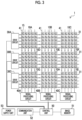
- FIG. 1 is a plan view showing an example of a configuration of a radiography apparatus 1 according to an embodiment of the disclosed technology.
- FIG. 2 is a cross-sectional view taken along line 2 - 2 in FIG. 1 .
- the radiography apparatus 1 has a radiation detector 10 having a so-called DDA configuration.
- the radiation detector 10 is partitioned into a plurality of blocks 10 A to 10 I.
- the plurality of blocks 10 A to 10 I are arranged in a matrix.
- Each of the blocks 10 A to 10 I is electrically and mechanically connected to an adjacent block via a connector 20 .
- the block 10 A is connected to the block 10 B adjacent in a horizontal direction in the drawing via the connector 20 , and is connected to the block 10 D adjacent in a vertical direction in the drawing via the connector 20 .
- FIG. 1 illustrates a case where the radiation detector 10 is partitioned into nine blocks 10 A to 10 I, the number of partitions (number of blocks) of the radiation detector 10 can be changed as appropriate.
- each of the blocks 10 A to 10 I of the radiation detector 10 has a substrate 11 provided with a plurality of pixels 15 (see FIG. 3 ), a scintillator 12 laminated on the substrate 11 , the connector 20 mounted on the substrate 11 , and a housing 13 accommodating the substrate 11 and the scintillator 12 therein. That is, the blocks 10 A to 10 I have separate substrates 11 and scintillators 12 .
- the substrate 11 is a flexible substrate having flexibility.
- a resin sheet containing a plastic such as polyimide (PI) can be used as a material of the substrate 11 .
- a thickness of the substrate 11 need only be such as to obtain desired flexibility depending on the hardness of the material, the size of the substrate 11 , and the like.
- a thickness of the resin sheet need only be, for example, 5 ⁇ m to 125 ⁇ m, and more preferably 20 ⁇ m to 50 ⁇ m.
- Specific examples of the resin sheet include XENOMAX (registered trademark).
- the scintillator 12 and the housing 13 each have flexibility, similarly to the substrate 11 .
- Gd 2 O 2 S: Tb (terbium-doped gadolinium oxysulfide) can be used as a material of the scintillator 12 .
- the housing 13 is made of a flexible resin having a relatively high transmittance for X-rays.
- the scintillator 12 side is an incident side of radiation.
- Each of the blocks 10 A to 10 I of the radiation detector 10 has the plurality of pixels 15 arranged in a matrix on the substrate 11 .
- Each of the plurality of pixels 15 includes a photoelectric conversion element 17 that generates an electric charge based on light emitted from the scintillator 12 , and a thin film transistor (TFT) 16 as a switching element which is turned on in a case where the electric charge generated in the photoelectric conversion elements 17 is read out.
- the photoelectric conversion element 17 may be, for example, a photodiode formed of amorphous silicon.
- a gate line 31 extending in one direction (row direction) along the arrangement of the pixels 15 and a signal line 41 extending in a direction (column direction) intersecting the extending direction of the gate line 31 are provided.
- Each of the pixels 15 is provided corresponding to each intersection part of the gate line 31 and the signal line 41 .
- the connection of the gate line 31 and the signal line 41 between the blocks of the radiation detector 10 is performed by the connector 20 .
- the gate line 31 of the block 10 A and the gate line 31 of the block 10 B are connected by the connector 20 that connects these blocks to each other.
- the signal line 41 of the block 10 A and the signal line 41 of the block 10 D are connected by the connector 20 that connects these blocks to each other.
- Each of the gate lines 31 extending over the blocks 10 A, 10 B, and 10 C of the radiation detector 10 is connected to a drive circuit 30 A.
- Each of the gate lines 31 extending over the blocks 10 D, 10 E, and 10 F of the radiation detector 10 is connected to a drive circuit 30 B.
- Each of the gate lines 31 extending over the blocks 10 G, 10 H, and 10 I of the radiation detector 10 is connected to a drive circuit 30 C. The connection between the blocks 10 A to 10 I of the radiation detector 10 and the drive circuits 30 A to 30 C will be described in detail below.
- Each of the signal lines 41 extending over the blocks 10 A, 10 D, and 10 G of the radiation detector 10 is connected to a signal processing circuit 40 A.
- Each of the signal lines 41 extending over the blocks 10 B, 10 E, and 10 H of the radiation detector 10 is connected to a signal processing circuit 40 B.
- Each of the signal lines 41 extending over the blocks 10 C, 10 F, and 10 I of the radiation detector 10 is connected to a signal processing circuit 40 C.
- the drive circuits 30 A, 30 B, and 30 C each output a drive signal based on a control signal supplied from a control unit 50 to read out the electric charge accumulated in the pixel 15 .
- the signal processing circuits 40 A, 40 B, and 40 C each generate image data by performing predetermined processing on an electric signal due to the electric charge read out from the pixel 15 based on the control signal supplied from the control unit 50 .
- the signal processing circuits 40 A, 40 B, and 40 C each comprise an amplification circuit that amplifies an input electric signal and a sample-and-hold circuit (neither shown) for each signal line 41 .
- the signal processing circuits 40 A, 40 B, and 40 C each have a multiplexer and an analog-to-digital (AD) converter (neither shown) provided in a subsequent stage of the sample-and-hold circuit.
- AD analog-to-digital
- the electric signals transmitted to the individual signal lines 41 are amplified by the amplification circuits and then held by the sample-and-hold circuits.
- the electric signals held by the individual sample-and-hold circuits are input (serially) in sequence to the multiplexer.
- the electric signals sequentially selected by the multiplexer are converted into digital image data by the AD converter.
- the pieces of image data generated by the signal processing circuits 40 A, 40 B, and 40 C are sequentially output to the control unit 50 and sequentially stored in an image memory 51 .
- the image memory 51 has a storage capacity capable of storing a predetermined number of image data, and each time a radiation image is captured, image data obtained by imaging is stored in the image memory 51 .
- the control unit 50 controls the operation of the radiography apparatus 1 by controlling the drive circuits 30 A, 30 B, and 30 C, the signal processing circuits 40 A, 40 B, and 40 C, and the image memory 51 .
- the control unit 50 may include a microcomputer comprising a central processing unit (CPU), a memory including a read only memory (ROM) and a random access memory (RAM), and a non-volatile storage unit such as a flash memory.
- a communication unit 52 is connected to the control unit 50 and transmits and receives various kinds of information to and from an external device by wireless communication.
- the communication unit 52 transmits the radiation image stored in the image memory 51 to an external device such as a personal computer.
- a power supply unit 53 supplies electric power to the drive circuits 30 A, 30 B, and 30 C, the signal processing circuits 40 A, 40 B, and 40 C, the image memory 51 , the control unit 50 , and the communication unit 52 .
- FIG. 3 in order to avoid the complexity of the drawing, wiring connecting the power supply unit 53 and various circuits is not shown.
- the drive circuits 30 A, 30 B, and 30 C are mounted on separate circuit boards 32 , respectively.
- the signal processing circuits 40 A, 40 B, and 40 C are mounted on separate circuit boards 42 , respectively.
- the circuit boards 32 and 42 are accommodated in a common case 60 , respectively.
- the case 60 accommodating the drive circuits 30 A, 30 B, and 30 C and the signal processing circuits 40 A, 40 B, and 40 C therein is provided along one side of the radiation detector 10 having the laminate including the scintillator 12 and the substrate 11 .
- the control unit 50 , the image memory 51 , the communication unit 52 , and the power supply unit 53 may be accommodated in the case 60 .
- Connectors 33 A, 33 B, and 33 C respectively corresponding to the drive circuits 30 A, 30 B, and 30 C are provided on a surface of the case 60 . Output terminals of the drive circuits 30 A, 30 B, and 30 C are led out to the corresponding connectors 33 A, 33 B, and 33 C, respectively, via flexible cables 34 .
- connectors 43 A, 43 B, and 43 C respectively corresponding to the signal processing circuits 40 A, 40 B, and 40 C are provided on the surface of the case 60 . Output terminals of the signal processing circuits 40 A, 40 B, and 40 C are led out to the corresponding connectors 43 A, 43 B, and 43 C, respectively, via flexible cables 44 .
- the gate lines 31 extending over the blocks 10 A, 10 B, and 10 C of the radiation detector 10 are led out to a connector 36 A at an end part of the block 10 A via a flexible cable 35 connected to the gate lines 31 .
- the drive signal output from the drive circuit 30 A is supplied to the gate lines 31 extending over the blocks 10 A, 10 B, and 10 C of the radiation detector 10 .
- the gate lines 31 extending over the blocks 10 D, 10 E, and 10 F of the radiation detector 10 are led out to a connector 36 B at an end part of the block 10 D via a flexible cable 35 connected to the gate lines 31 .
- the drive signal output from the drive circuit 30 B is supplied to the gate lines 31 extending over the blocks 10 D, 10 E, and 10 F of the radiation detector 10 .
- the gate lines 31 extending over the blocks 10 G, 10 H, and 10 I of the radiation detector 10 are led out to a connector 36 C at an end part of the block 10 G via a flexible cable 35 connected to the gate lines 31 .
- the drive signal output from the drive circuit 30 C is supplied to the gate lines 31 extending over the blocks 10 G, 10 H, and 10 I of the radiation detector 10 .
- the signal lines 41 extending over the blocks 10 A, 10 D, and 10 G of the radiation detector 10 are led out to a connector 46 A at an end part of the block 10 A via a flexible cable 45 connected to the signal lines 41 .
- the connector 46 A led out from the radiation detector 10 and the connector 43 A led out from the signal processing circuit 40 A are connected to each other, the electric signals transmitted to the signal lines 41 extending over the blocks 10 A, 10 D, and 10 G of the radiation detector 10 are supplied to the signal processing circuit 40 A.
- the signal lines 41 extending over the blocks 10 B, 10 E, and 10 H of the radiation detector 10 are led out to a connector 46 B at an end part of the block 10 B via a flexible cable 45 connected to the signal lines 41 .
- the connector 46 B led out from the radiation detector 10 and the connector 43 B led out from the signal processing circuit 40 B are connected to each other, the electric signals transmitted to the signal lines 41 extending over the blocks 10 B, 10 E, and 10 H of the radiation detector 10 are supplied to the signal processing circuit 40 B.
- the signal lines 41 extending over the blocks 10 C, 10 F, and 10 I of the radiation detector 10 are led out to a connector 46 C at an end part of the block 10 C via a flexible cable 45 connected to the signal lines 41 .
- the connector 46 C led out from the radiation detector 10 and the connector 43 C led out from the signal processing circuit 40 C are connected to each other, the electric signals transmitted to the signal lines 41 extending over the blocks 10 C, 10 F, and 10 I of the radiation detector 10 are supplied to the signal processing circuit 40 C.
- the scintillator 12 absorbs the radiation and emits visible light.
- the photoelectric conversion element 17 constituting the pixel 15 converts the light emitted from the scintillator 12 into an electric charge.
- the electric charge generated by the photoelectric conversion element 17 is accumulated in the corresponding pixel 15 .
- the amount of electric charge generated by the photoelectric conversion element 17 is reflected in a pixel value of the corresponding pixel 15 .
- the drive circuits 30 A, 30 B, and 30 C supply the drive signal to the TFT 16 via the gate lines 31 based on the control signal supplied from the control unit 50 .
- the TFT 16 is turned on in units of rows by the drive signal. In a case where the TFT 16 is turned on, the electric charge accumulated in the pixel 15 is read out to the signal line 41 and supplied to the signal processing circuits 40 A, 40 B, and 40 C.
- Each of the signal processing circuits 40 A to 40 C includes an amplification circuit, a sample-and-hold circuit, a multiplexer, and an AD converter (not shown).
- the electric signals transmitted to the individual signal lines 41 are amplified by the amplification circuits and then held by the sample-and-hold circuits.
- the electric signals held by the individual sample-and-hold circuits are input (serially) in sequence to the multiplexer.
- the electric signals sequentially selected by the multiplexer are converted into digital signals by the AD converter.
- the signal processing circuits 40 A, 40 B, and 40 C generate data in which the digital signal is associated with position information of the pixel 15 as image data.
- the image memory 51 stores the image data generated by the signal processing circuits 40 A, 40 B, and 40 C.
- FIGS. 5 A and 5 B are diagram showing an example of the configuration of the connector 20 that connects the blocks of the radiation detector 10 to each other.
- FIGS. 5 A and 5 B show, as an example, a connector for connecting the block 10 A and the block 10 B of the radiation detector 10 to each other.
- a reference numeral 20 A is given to the connector provided in the block 10 A
- a reference numeral 20 B is given to the connector provided in the block 10 B.
- the connector 20 A provided in the block 10 A of the radiation detector 10 has a conductive portion 21 A connected to the gate line 31 on the substrate 11 constituting the block 10 A.
- a plurality of the conductive portions 21 A are provided corresponding to each of a plurality of the gate lines on the substrate 11 constituting the block 10 A.
- a periphery of the conductive portion 21 A is covered with an insulating portion 22 A.
- the plurality of conductive portions 21 A are insulated from each other by the insulating portion 22 A.
- a material of the conductive portion 21 A for example, a silicone rubber in which conductive fine particles such as silver-based fine powder are dispersed can be used.
- As a material of the insulating portion 22 A for example, an insulating silicone rubber can be used. Since both the conductive portion 21 A and the insulating portion 22 A are made of a flexible material such as a silicone rubber, the connector 20 A has flexibility as a whole.
- the connector 20 B provided in the block 10 B of the radiation detector 10 has a conductive portion 21 B connected to the gate line 31 on the substrate 11 constituting the block 10 B.
- a plurality of the conductive portions 21 B are provided corresponding to each of a plurality of the gate lines on the substrate 11 constituting the block 10 B.
- a periphery of the conductive portion 21 B is covered with an insulating portion 22 B.
- the plurality of conductive portions 21 B are insulated from each other by the insulating portion 22 B.
- As a material of the conductive portion 21 B the same material as that of the conductive portion 21 A can be used.
- As a material of the insulating portion 22 B the same material as that of the insulating portion 22 A can be used. Since both the conductive portion 21 B and the insulating portion 22 B are made of a flexible material such as a silicone rubber, the connector 20 B has flexibility as a whole.
- the conductive portion 21 A of the connector 20 A has a concave portion 23
- the conductive portion 21 B of the connector 20 B has a convex portion 24 .
- the convex portion 24 of the conductive portion 21 B is fitted into the concave portion 23 of the conductive portion 21 A
- the conductive portion 21 A and the conductive portion 21 B are connected to each other
- the block 10 A and the block 10 B of the radiation detector 10 are electrically and mechanically connected to each other. That is, each of the gate lines 31 of the block 10 A is connected to each of the corresponding gate lines 31 of the block 10 B.
- the joining between the connector 20 A and the connector 20 B can be released by applying a force in a direction in which the connector 20 A and the connector 20 B are separated from each other.
- the block 10 B of the radiation detector 10 can be separated from the block 10 A. That is, after the connector 20 A and the connector 20 B are joined together, the state shown in FIG. 5 A can be achieved. Thereafter, the state (that is, the state shown in FIG. 5 B ) in which the connector 20 A and the connector 20 B are joined together can also be achieved.
- the radiography apparatus 1 includes the scintillator 12 and the substrate 11 that is laminated on the scintillator 12 and has a plurality of the photoelectric conversion elements 17 converting light emitted from the scintillator 12 into the electric charges.
- the radiation detector 10 comprising the laminate including the scintillator 12 and the substrate 11 is partitioned into the plurality of blocks 10 A to 10 I.
- Each of the plurality of blocks 10 A to 10 I has the connector 20 provided in a boundary portion with another block, and the blocks are separable from each other.
- the radiography apparatus 1 has, in each of the blocks 10 A to 10 I, a plurality of the TFTs 16 as the switching elements provided on the substrate 11 and provided corresponding to the plurality of photoelectric conversion elements 17 , a plurality of the gate lines 31 provided on the substrate 11 and transmitting the drive signals for driving the plurality of TFTs 16 , and a plurality of the signal lines 41 provided on the substrate 11 and transmitting the electric signals based on the electric charges generated by the plurality of photoelectric conversion elements 17 .
- the radiography apparatus 1 has a plurality of the drive circuits 30 A, 30 B, and 30 C connected to some different gate lines 31 among the plurality of gate lines 31 and outputting the drive signals for driving the TFTs 16 , respectively, and a plurality of the signal processing circuits 40 A, 40 B, and 40 C connected to some different signal lines 41 among the plurality of signal lines 41 and processing the electric signals transmitted to the signal lines 41 , respectively.
- the gate lines 31 included in the block are connected to one of the plurality of drive circuits 30 A, 30 B, and 30 C. That is, the gate lines 31 included in one block are not connected across a plurality of different drive circuits. For example, each of the gate lines 31 extending over the blocks 10 A, 10 B, and 10 C is connected only to the drive circuit 30 A and not to the other drive circuits 30 B and 30 C.
- each of the plurality of blocks 10 A to 10 I the signal lines 41 included in the block are connected to one of the plurality of signal processing circuits 40 A, 40 B, and 40 C. That is, the signal lines 41 included in one block are not connected across a plurality of different signal processing circuits.
- each of the signal lines 41 extending over the blocks 10 A, 10 D, and 10 G is connected only to the signal processing circuit 40 A and not to the other signal processing circuits 40 B and 40 C.
- the partition of the radiation detector 10 is defined by the drive circuits 30 A to 30 C and the signal processing circuits 40 A to 40 C.
- the radiation detector 10 since the substrate 11 , the scintillator 12 , and the housing 13 constituting each of the blocks 10 A to 10 I of the radiation detector 10 have flexibility, the radiation detector 10 has flexibility as a whole. Therefore, the radiation detector 10 can be wound around the surface of the pipe. Accordingly, the radiography apparatus 1 can be used for non-destructive testing of the welded portion of the pipe. Since there is a gap in the boundary portion between the blocks 10 A to 10 I of the radiation detector 10 , an image of the gap is missed.
- FIGS. 6 A to 6 E is a plan view illustrating an aspect of separation of the blocks of the radiation detector 10 .
- FIG. 6 A shows a state of separation of the blocks 10 G, 10 H, and 10 I of the radiation detector 10
- FIG. 6 B shows a state of separation of the blocks 10 D, 10 E, 10 F, 10 G, 10 H, and 10 I of the radiation detector 10
- FIG. 6 C shows a state of separation of the blocks 10 C, 10 F, and 10 I of the radiation detector 10
- FIG. 6 D shows a state of separation of the blocks 10 B, 10 E, 10 H, 10 C, 10 F, and 10 I of the radiation detector 10
- FIG. 6 E shows a state of separation of the blocks 10 E, 10 F, 10 H, and 10 I of the radiation detector 10 .
- the supply of the drive signal via the gate line 31 and the transmission of the electric signal via the signal line 41 to each block other than the separated blocks are not interrupted, and the capturing of the radiation image can be properly performed in each block other than the separated blocks.
- the shape and size of the radiation detector 10 can be changed at the imaging site.
- the shape and size of the radiation detector 10 is adapted to the shape and size of the pipe by appropriately separating the blocks of the radiation detector 10 in accordance with the shape and size of the pipe. In addition, it is possible to reconnect the separated blocks.
- the use of the radiation detector 10 is enabled by replacing only the some blocks in which the failure or damage occurs. As a result, it is possible to suppress the repair cost of the radiation detector 10 .
- the blocks 10 A to 10 I of the radiation detector 10 correspond to the drive circuits 30 A to 30 C and the signal processing circuits 40 A to 40 C. Therefore, the design of the radiography apparatus in the structural and control aspects is facilitated.
- each of the gate lines 31 included in one block is connected to one of the plurality of drive circuits 30 A to 30 C, and each of the signal lines 41 included in one block is connected to one of the plurality of signal processing circuits 40 A to 40 C.
- the size of one block can be reduced as compared with a case where each of the gate lines 31 included in one block is connected to any two or more of the plurality of drive circuits 30 A to 30 C, and each of the signal lines 41 included in one block is connected to any two or more of the plurality of signal processing circuits 40 A to 40 C.
- the shape and size of the radiation detector 10 can be changed more flexibly.
- the drive circuits 30 A, 30 B, and 30 C and the signal processing circuits 40 A, 40 B, and 40 C are provided along one side of the radiation detector 10 .
- the drive circuits 30 A, 30 B, and 30 C are provided along a first side of the radiation detector 10 , and the signal processing circuits 40 A, 40 B, and 40 C are provided along a second side intersecting the first side, it may be difficult to use the radiation detector 10 in a bent manner.
- the drive circuits 30 A, 30 B, and 30 C are provided along the first side of the radiation detector 10 , and the signal processing circuits 40 A, 40 B, and 40 C are provided along the second side opposite to the first side, the drive circuits 30 A, 30 B, and 30 C are separated from the signal processing circuits 40 A, 40 B, and 40 C. Therefore, the leading of wiring from the control unit 50 is complicated.
- the drive circuits 30 A, 30 B, and 30 C and the signal processing circuits 40 A, 40 B, and 40 C are provided along one side of the radiation detector 10 . Therefore, the radiation detector 10 can be used in a bent manner, and the complication of the leading of the wiring from the control unit 50 can be suppressed.
- FIG. 7 is a plan view showing an example of a configuration of a radiography apparatus 1 A according to a second embodiment of the disclosed technology.
- the radiography apparatus 1 A is different from the radiography apparatus 1 according to the first embodiment in the block configuration of the radiation detector 10 . That is, the radiation detector 10 according to the present embodiment is partitioned into three blocks 10 J, 10 K, and 10 L.
- the block 10 J is an integrated block of the blocks 10 A, 10 B, and 10 C according to the first embodiment. That is, the block 10 J includes the entire gate line 31 through which the drive signal output from the drive circuit 30 A is transmitted.
- the block 10 K is an integrated block of the blocks 10 D, 10 E, and 10 F according to the first embodiment. That is, the block 10 K includes the entire gate line 31 through which the drive signal output from the drive circuit 30 B is transmitted.
- the block 10 L is an integrated block of the blocks 10 G, 10 H, and 10 I according to the first embodiment. That is, the block 10 L includes the entire gate line 31 through which the drive signal output from the drive circuit 30 C is transmitted.
- FIGS. 8 A and 8 B is a plan view illustrating an aspect of separation of the blocks of the radiation detector 10 .
- FIG. 8 A shows a state of separation of the block 10 L of the radiation detector 10
- FIG. 8 B shows a state of separation of the blocks 10 K and 10 L of the radiation detector 10 .
- the shape and size of the radiation detector 10 can be changed at the imaging site.
- FIG. 9 is a plan view showing an example of a configuration of a radiography apparatus 1 B according to a third embodiment of the disclosed technology.
- the radiography apparatus 1 B is different from the radiography apparatus 1 according to the first embodiment in the block configuration of the radiation detector 10 . That is, the radiation detector 10 according to the present embodiment is partitioned into three blocks 10 M, 10 N, and 10 O.
- the block 10 M is an integrated block of the blocks 10 A, 10 D, and 10 G according to the first embodiment. That is, the block 10 M includes the entire signal line 41 through which the electric signal supplied to the signal processing circuit 40 A is transmitted.
- the block 10 N is an integrated block of the blocks 10 B, 10 E, and 10 H according to the first embodiment. That is, the block 10 N includes the entire signal line 41 through which the electric signal supplied to the signal processing circuit 40 B is transmitted.
- the block 10 O is an integrated block of the blocks 10 C, 10 F, and 10 I according to the first embodiment. That is, the block 10 O includes the entire signal line 41 through which the electric signal supplied to the signal processing circuit 40 C is transmitted.
- FIGS. 10 A and 10 B is a plan view illustrating an aspect of separation of the blocks of the radiation detector 10 .
- FIG. 10 A shows a state of separation of the block 10 O of the radiation detector 10
- FIG. 10 B shows a state of separation of the blocks 10 N and 10 O of the radiation detector 10 .
- the shape and size of the radiation detector 10 can be changed at the imaging site.
- FIG. 11 is a plan view showing an example of a configuration of a radiography apparatus 1 C according to a fourth embodiment of the disclosed technology.
- the radiation detector 10 is partitioned into a plurality of blocks 10 A to 10 P.
- the radiography apparatus 1 C has drive circuits 30 A, 30 B, 30 C, and 30 D and signal processing circuits 40 A, 40 B, 40 C, and 40 D.
- a case 60 L accommodating the drive circuits 30 A and 30 B and the signal processing circuits 40 A and 40 B therein is provided along the first side of the radiation detector 10 .
- a case 60 R accommodating the drive circuits 30 C and 30 D and the signal processing circuits 40 C and 40 D therein is provided along the second side of the radiation detector 10 opposite to the first side.
- the drive circuits 30 A and 30 B and the signal processing circuits 40 A and 40 B are provided on one end side of the radiation detector 10
- the drive circuits 30 C and 30 D and the signal processing circuits 40 C and 40 D are provided on the other end side of the radiation detector 10 .
- Each of the gate lines 31 extending over the blocks 10 A, 10 B, 10 C, and 10 D of the radiation detector 10 is connected to the drive circuit 30 A.
- Each of the gate lines 31 extending over the blocks 10 E, 10 F, 10 G, and 10 H of the radiation detector 10 is connected to the drive circuit 30 B.
- Each of the gate lines 31 extending over the blocks 10 I, 10 J, 10 K, and 10 L of the radiation detector 10 is connected to the drive circuit 30 C.
- Each of the gate lines 31 extending over the blocks 10 M, 10 N, 10 O, and 10 P of the radiation detector 10 is connected to the drive circuit 30 D.
- Each of the signal lines 41 extending over the blocks 10 A, 10 E, 10 I, and 10 M of the radiation detector 10 is connected to the signal processing circuit 40 A.
- Each of the signal lines 41 extending over the blocks 10 B, 10 F, 10 J, and 10 N of the radiation detector 10 is connected to the signal processing circuit 40 B.
- Each of the signal lines 41 extending over the blocks 10 C, 10 G, 10 K, and 10 O of the radiation detector 10 is connected to the signal processing circuit 40 C.
- Each of the signal lines 41 extending over the blocks 10 D, 10 H, 10 L, and 10 P of the radiation detector 10 is connected to the signal processing circuit 40 D.
- the drive circuits 30 A, 30 B, 30 C, and 30 D each output the drive signal based on the control signal supplied from the control unit 50 to read out the electric charge accumulated in the pixel 15 .
- the drive circuits 30 A, 30 B, 30 C, and 30 D are electrically connected to each other, and the drive circuits can operate in cooperation with each other.
- the drive circuits 30 A, 30 B, 30 C, and 30 D can operate in cooperation with each other such that the drive signals are sequentially output from the drive circuits 30 A, 30 B, 30 C, and 30 D.
- the drive circuits 30 A, 30 B, 30 C, and 30 D may operate independently without cooperating with each other.
- the electrical connection among the drive circuits 30 A, 30 B, 30 C, and 30 D can be realized by wire or wireless.
- the signal processing circuits 40 A, 40 B, 40 C, and 40 D each generate image data by performing predetermined processing on an electric signal due to the electric charge read out from the pixel 15 based on the control signal supplied from the control unit 50 .
- the signal processing circuits 40 A, 40 B, 40 C, and 40 D are electrically connected to each other, and the signal processing circuits can operate in cooperation with each other.
- the signal processing circuits 40 A, 40 B, 40 C, and 40 D can operate in cooperation with each other such that the pieces of image data are sequentially output from the signal processing circuits 40 A, 40 B, 40 C, and 40 D.
- the signal processing circuits 40 A, 40 B, 40 C, and 40 D may operate independently without cooperating with each other.
- the electrical connection among the signal processing circuits 40 A, 40 B, 40 C, and 40 D can be realized by wire or wireless.
- each block of the radiation detector 10 may be separated in an aspect in which reconnection is not possible.
Landscapes
- Physics & Mathematics (AREA)
- Health & Medical Sciences (AREA)
- Life Sciences & Earth Sciences (AREA)
- General Physics & Mathematics (AREA)
- High Energy & Nuclear Physics (AREA)
- Molecular Biology (AREA)
- Spectroscopy & Molecular Physics (AREA)
- Measurement Of Radiation (AREA)
- Apparatus For Radiation Diagnosis (AREA)
Abstract
Description
-
- 1A, 1B: radiography apparatus
- 10: radiation detector
- 10A to 10O: block
- 11: substrate
- 12: scintillator
- 13: housing
- 15: pixel
- 16: TFT
- 17: photoelectric conversion element
- 20, 20A, 20B: connector
- 21A, 21B: conductive portion
- 22A, 22B: insulating portion
- 23: concave portion
- 24: convex portion
- 30: drive circuit
- 30A, 30B, 30C: drive circuit
- 31: gate line
- 32: circuit board
- 33A, 33B, 33C: connector
- 34, 35: flexible cable
- 36A, 36B, 36C: connector
- 40A, 40B, 40C: signal processing circuit
- 41: signal line
- 42: circuit board
- 43A, 43B, 43C: connector
- 44, 45: flexible cable
- 46A, 46B, 46C: connector
- 50: control unit
- 51: image memory
- 52: communication unit
- 53: power supply unit
- 60: case
Claims (7)
Applications Claiming Priority (3)
| Application Number | Priority Date | Filing Date | Title |
|---|---|---|---|
| JP2019046327 | 2019-03-13 | ||
| JP2019-046327 | 2019-03-13 | ||
| PCT/JP2019/042940 WO2020183778A1 (en) | 2019-03-13 | 2019-10-31 | Radiographic imaging device |
Related Parent Applications (1)
| Application Number | Title | Priority Date | Filing Date |
|---|---|---|---|
| PCT/JP2019/042940 Continuation-In-Part WO2020183778A1 (en) | 2019-03-13 | 2019-10-31 | Radiographic imaging device |
Publications (2)
| Publication Number | Publication Date |
|---|---|
| US20210389480A1 US20210389480A1 (en) | 2021-12-16 |
| US12117572B2 true US12117572B2 (en) | 2024-10-15 |
Family
ID=72426655
Family Applications (1)
| Application Number | Title | Priority Date | Filing Date |
|---|---|---|---|
| US17/412,758 Active 2039-12-17 US12117572B2 (en) | 2019-03-13 | 2021-08-26 | Radiography apparatus |
Country Status (4)
| Country | Link |
|---|---|
| US (1) | US12117572B2 (en) |
| JP (1) | JP7102605B2 (en) |
| CN (1) | CN113574416B (en) |
| WO (1) | WO2020183778A1 (en) |
Families Citing this family (1)
| Publication number | Priority date | Publication date | Assignee | Title |
|---|---|---|---|---|
| US12352709B2 (en) * | 2022-03-01 | 2025-07-08 | Baker Hughes Holdings Llc | Flexible digital detector array |
Citations (14)
| Publication number | Priority date | Publication date | Assignee | Title |
|---|---|---|---|---|
| JP2010078543A (en) | 2008-09-29 | 2010-04-08 | Fujifilm Corp | Radiation detector |
| JP2011227047A (en) | 2010-03-29 | 2011-11-10 | Fujifilm Corp | Radiation imaging apparatus and radiation imaging system |
| US20120126128A1 (en) | 2010-11-22 | 2012-05-24 | Canon Kabushiki Kaisha | Radiation detection apparatus and radiation detection system |
| CN102918419A (en) | 2010-05-31 | 2013-02-06 | 富士胶片株式会社 | Radiographic imaging device |
| US20130048866A1 (en) | 2011-08-26 | 2013-02-28 | Fujifilm Corporation | Radiation detector and radiological image radiographing apparatus |
| US20130306875A1 (en) * | 2012-05-18 | 2013-11-21 | General Electric Company | Tiled x-ray imager panel and method of forming the same |
| JP2014102202A (en) | 2012-11-21 | 2014-06-05 | Fujifilm Corp | Perspective image density correction method, nondestructive inspection method, and image processing apparatus |
| WO2016017305A1 (en) | 2014-07-31 | 2016-02-04 | ソニー株式会社 | Pixel circuit, semiconductor light detection device, and radiation measuring device |
| US20160220217A1 (en) | 2015-01-30 | 2016-08-04 | Canon Kabushiki Kaisha | Radiographing apparatus, control apparatus, control method, and storage medium |
| JP2016140511A (en) | 2015-01-30 | 2016-08-08 | キヤノン株式会社 | Radiographing system, radiographing apparatus, control device, control method, and program |
| CN106549277A (en) | 2015-09-22 | 2017-03-29 | 泰科电子(上海)有限公司 | Board to board connector |
| JP2017062210A (en) | 2015-09-25 | 2017-03-30 | 株式会社ブイ・テクノロジー | Radiation image imaging apparatus |
| WO2017202738A1 (en) | 2016-05-26 | 2017-11-30 | Koninklijke Philips N.V. | Multifunctional radiation detector |
| US20180333121A1 (en) | 2017-05-18 | 2018-11-22 | Fujifilm Corporation | Radiography system, radiography method, radiography program, and body thickness estimation apparatus |
-
2019
- 2019-10-31 CN CN201980093970.1A patent/CN113574416B/en active Active
- 2019-10-31 WO PCT/JP2019/042940 patent/WO2020183778A1/en not_active Ceased
- 2019-10-31 JP JP2021505496A patent/JP7102605B2/en active Active
-
2021
- 2021-08-26 US US17/412,758 patent/US12117572B2/en active Active
Patent Citations (22)
| Publication number | Priority date | Publication date | Assignee | Title |
|---|---|---|---|---|
| JP2010078543A (en) | 2008-09-29 | 2010-04-08 | Fujifilm Corp | Radiation detector |
| JP2011227047A (en) | 2010-03-29 | 2011-11-10 | Fujifilm Corp | Radiation imaging apparatus and radiation imaging system |
| CN102918419A (en) | 2010-05-31 | 2013-02-06 | 富士胶片株式会社 | Radiographic imaging device |
| US20130082184A1 (en) | 2010-05-31 | 2013-04-04 | Fujifilm Corporation | Radiographic imaging device |
| US20120126128A1 (en) | 2010-11-22 | 2012-05-24 | Canon Kabushiki Kaisha | Radiation detection apparatus and radiation detection system |
| CN102540235A (en) | 2010-11-22 | 2012-07-04 | 佳能株式会社 | Radiation detection apparatus and radiation detection system |
| US20130048866A1 (en) | 2011-08-26 | 2013-02-28 | Fujifilm Corporation | Radiation detector and radiological image radiographing apparatus |
| CN102949197A (en) | 2011-08-26 | 2013-03-06 | 富士胶片株式会社 | Radiation detector and radiological image radiographing apparatus |
| US20130306875A1 (en) * | 2012-05-18 | 2013-11-21 | General Electric Company | Tiled x-ray imager panel and method of forming the same |
| US20150235357A1 (en) | 2012-11-21 | 2015-08-20 | Fujifilm Corporation | Fluoroscopic image density correction method, non-destructive inspection method, and image processing device |
| JP2014102202A (en) | 2012-11-21 | 2014-06-05 | Fujifilm Corp | Perspective image density correction method, nondestructive inspection method, and image processing apparatus |
| WO2016017305A1 (en) | 2014-07-31 | 2016-02-04 | ソニー株式会社 | Pixel circuit, semiconductor light detection device, and radiation measuring device |
| US20170207257A1 (en) | 2014-07-31 | 2017-07-20 | Sony Semiconductor Solutions Corporation | Pixel circuit, semiconductor photodetection device, and radiation counting device |
| US20160220217A1 (en) | 2015-01-30 | 2016-08-04 | Canon Kabushiki Kaisha | Radiographing apparatus, control apparatus, control method, and storage medium |
| JP2016140511A (en) | 2015-01-30 | 2016-08-08 | キヤノン株式会社 | Radiographing system, radiographing apparatus, control device, control method, and program |
| CN106549277A (en) | 2015-09-22 | 2017-03-29 | 泰科电子(上海)有限公司 | Board to board connector |
| JP2017062210A (en) | 2015-09-25 | 2017-03-30 | 株式会社ブイ・テクノロジー | Radiation image imaging apparatus |
| WO2017202738A1 (en) | 2016-05-26 | 2017-11-30 | Koninklijke Philips N.V. | Multifunctional radiation detector |
| CN109196385A (en) | 2016-05-26 | 2019-01-11 | 皇家飞利浦有限公司 | Multifunctional radiation detector |
| US20190120977A1 (en) * | 2016-05-26 | 2019-04-25 | Koninklijke Philips N.V. | Multifunctional radiation detector |
| US20180333121A1 (en) | 2017-05-18 | 2018-11-22 | Fujifilm Corporation | Radiography system, radiography method, radiography program, and body thickness estimation apparatus |
| CN108937982A (en) | 2017-05-18 | 2018-12-07 | 富士胶片株式会社 | Radiation image picking-up system, radiation image photography method, program storage medium and body thickness apparatus for predicting |
Non-Patent Citations (6)
| Title |
|---|
| Chinese Office Action dated Apr. 17, 2024 in Application No. 201980093970.1. |
| Chinese Office Action issued Nov. 9, 2023 in Application No. 201980093970.1. |
| International Preliminary Report on Patentability dated Aug. 25, 2021 with a Translation of the Written Opinion of the International Searching Authority in Application No. PCT/JP2019/042940. |
| International Search Report dated Jan. 21, 2020 in Application No. PCT/JP2019/042940. |
| Notice of Reasons for Refusal dated Mar. 29, 2022 from the Japanese Patent Office in JP Application No. 2021-505496. |
| Written Opinion of the International Searching Authority dated Jan. 21, 2020 in Application No. PCT/JP2019/042940. |
Also Published As
| Publication number | Publication date |
|---|---|
| JPWO2020183778A1 (en) | 2021-10-14 |
| JP7102605B2 (en) | 2022-07-19 |
| WO2020183778A1 (en) | 2020-09-17 |
| CN113574416B (en) | 2024-09-17 |
| CN113574416A (en) | 2021-10-29 |
| US20210389480A1 (en) | 2021-12-16 |
Similar Documents
| Publication | Publication Date | Title |
|---|---|---|
| US8067743B2 (en) | Imaging apparatus and radiation imaging apparatus | |
| US9306108B2 (en) | Radiation detector | |
| CN104350737B (en) | X-ray imaging apparatus and radiation detector | |
| US11415715B2 (en) | Radiation image capturing apparatus | |
| US11520057B2 (en) | Radiation image capturing apparatus | |
| JP6505973B2 (en) | Portable radiography system | |
| US12117572B2 (en) | Radiography apparatus | |
| US20180275292A1 (en) | Radiographic imaging apparatus | |
| CN109073766A (en) | Chip-on-chip film repair on flexible substrates | |
| US10317540B2 (en) | Radiation detector and radiographic imaging apparatus | |
| JP6719324B2 (en) | Radiation imaging apparatus and radiation imaging system | |
| JP6731757B2 (en) | Radiation imaging apparatus and radiation imaging system | |
| KR102747067B1 (en) | X-ray detector | |
| US12239475B2 (en) | Radiation image detector comprising a plurality of gate control circuits, a plurality of readout control circuits, and a power supply circuit | |
| TWI802655B (en) | Radiographic imaging device | |
| JP2021049204A (en) | Radiation imaging device and radiation imaging system |
Legal Events
| Date | Code | Title | Description |
|---|---|---|---|
| AS | Assignment |
Owner name: FUJIFILM CORPORATION, JAPAN Free format text: ASSIGNMENT OF ASSIGNORS INTEREST;ASSIGNORS:NOMURA, KENGO;NARUKAWA, YASUNORI;REEL/FRAME:057301/0076 Effective date: 20210616 |
|
| FEPP | Fee payment procedure |
Free format text: ENTITY STATUS SET TO UNDISCOUNTED (ORIGINAL EVENT CODE: BIG.); ENTITY STATUS OF PATENT OWNER: LARGE ENTITY |
|
| STPP | Information on status: patent application and granting procedure in general |
Free format text: DOCKETED NEW CASE - READY FOR EXAMINATION |
|
| STPP | Information on status: patent application and granting procedure in general |
Free format text: RESPONSE TO NON-FINAL OFFICE ACTION ENTERED AND FORWARDED TO EXAMINER |
|
| STPP | Information on status: patent application and granting procedure in general |
Free format text: FINAL REJECTION MAILED |
|
| STPP | Information on status: patent application and granting procedure in general |
Free format text: ADVISORY ACTION MAILED |
|
| STPP | Information on status: patent application and granting procedure in general |
Free format text: DOCKETED NEW CASE - READY FOR EXAMINATION |
|
| STPP | Information on status: patent application and granting procedure in general |
Free format text: NON FINAL ACTION MAILED |
|
| STPP | Information on status: patent application and granting procedure in general |
Free format text: RESPONSE TO NON-FINAL OFFICE ACTION ENTERED AND FORWARDED TO EXAMINER |
|
| STPP | Information on status: patent application and granting procedure in general |
Free format text: NOTICE OF ALLOWANCE MAILED -- APPLICATION RECEIVED IN OFFICE OF PUBLICATIONS |
|
| ZAAA | Notice of allowance and fees due |
Free format text: ORIGINAL CODE: NOA |
|
| ZAAB | Notice of allowance mailed |
Free format text: ORIGINAL CODE: MN/=. |
|
| STPP | Information on status: patent application and granting procedure in general |
Free format text: AWAITING TC RESP., ISSUE FEE NOT PAID |
|
| STPP | Information on status: patent application and granting procedure in general |
Free format text: NOTICE OF ALLOWANCE MAILED -- APPLICATION RECEIVED IN OFFICE OF PUBLICATIONS |
|
| STPP | Information on status: patent application and granting procedure in general |
Free format text: PUBLICATIONS -- ISSUE FEE PAYMENT VERIFIED |
|
| STCF | Information on status: patent grant |
Free format text: PATENTED CASE |