US12102004B2 - Compound for organic electronic element, organic electronic element using the same, and an electronic device thereof - Google Patents

Compound for organic electronic element, organic electronic element using the same, and an electronic device thereof Download PDF

Info

Publication number
US12102004B2
US12102004B2 US18/413,635 US202418413635A US12102004B2 US 12102004 B2 US12102004 B2 US 12102004B2 US 202418413635 A US202418413635 A US 202418413635A US 12102004 B2 US12102004 B2 US 12102004B2
Authority
US
United States
Prior art keywords
group
ring
organic
compound
electronic element
Prior art date
Legal status (The legal status is an assumption and is not a legal conclusion. Google has not performed a legal analysis and makes no representation as to the accuracy of the status listed.)
Active
Application number
US18/413,635
Other versions
US20240206334A1 (en
Inventor
Hyun Ju Song
Hyo Min Jin
Junggeun LEE
Current Assignee (The listed assignees may be inaccurate. Google has not performed a legal analysis and makes no representation or warranty as to the accuracy of the list.)
DukSan Neolux Co Ltd
Original Assignee
DukSan Neolux Co Ltd
Priority date (The priority date is an assumption and is not a legal conclusion. Google has not performed a legal analysis and makes no representation as to the accuracy of the date listed.)
Filing date
Publication date
Priority claimed from US17/096,790 external-priority patent/US11063226B1/en
Priority claimed from US18/180,625 external-priority patent/US20230225206A1/en
Application filed by DukSan Neolux Co Ltd filed Critical DukSan Neolux Co Ltd
Priority to US18/413,635 priority Critical patent/US12102004B2/en
Assigned to DUK SAN NEOLUX CO., LTD. reassignment DUK SAN NEOLUX CO., LTD. ASSIGNMENT OF ASSIGNORS INTEREST (SEE DOCUMENT FOR DETAILS). Assignors: JIN, HYO MIN, LEE, Junggeun, SONG, HYUN JU
Publication of US20240206334A1 publication Critical patent/US20240206334A1/en
Application granted granted Critical
Publication of US12102004B2 publication Critical patent/US12102004B2/en
Active legal-status Critical Current
Anticipated expiration legal-status Critical

Links

Images

Classifications

    • CCHEMISTRY; METALLURGY
    • C07ORGANIC CHEMISTRY
    • C07DHETEROCYCLIC COMPOUNDS
    • C07D251/00Heterocyclic compounds containing 1,3,5-triazine rings
    • C07D251/02Heterocyclic compounds containing 1,3,5-triazine rings not condensed with other rings
    • C07D251/12Heterocyclic compounds containing 1,3,5-triazine rings not condensed with other rings having three double bonds between ring members or between ring members and non-ring members
    • C07D251/14Heterocyclic compounds containing 1,3,5-triazine rings not condensed with other rings having three double bonds between ring members or between ring members and non-ring members with hydrogen or carbon atoms directly attached to at least one ring carbon atom
    • C07D251/24Heterocyclic compounds containing 1,3,5-triazine rings not condensed with other rings having three double bonds between ring members or between ring members and non-ring members with hydrogen or carbon atoms directly attached to at least one ring carbon atom to three ring carbon atoms
    • CCHEMISTRY; METALLURGY
    • C07ORGANIC CHEMISTRY
    • C07DHETEROCYCLIC COMPOUNDS
    • C07D307/00Heterocyclic compounds containing five-membered rings having one oxygen atom as the only ring hetero atom
    • C07D307/77Heterocyclic compounds containing five-membered rings having one oxygen atom as the only ring hetero atom ortho- or peri-condensed with carbocyclic rings or ring systems
    • C07D307/91Dibenzofurans; Hydrogenated dibenzofurans
    • CCHEMISTRY; METALLURGY
    • C07ORGANIC CHEMISTRY
    • C07DHETEROCYCLIC COMPOUNDS
    • C07D333/00Heterocyclic compounds containing five-membered rings having one sulfur atom as the only ring hetero atom
    • C07D333/50Heterocyclic compounds containing five-membered rings having one sulfur atom as the only ring hetero atom condensed with carbocyclic rings or ring systems
    • C07D333/76Dibenzothiophenes
    • CCHEMISTRY; METALLURGY
    • C07ORGANIC CHEMISTRY
    • C07DHETEROCYCLIC COMPOUNDS
    • C07D409/00Heterocyclic compounds containing two or more hetero rings, at least one ring having sulfur atoms as the only ring hetero atoms
    • C07D409/02Heterocyclic compounds containing two or more hetero rings, at least one ring having sulfur atoms as the only ring hetero atoms containing two hetero rings
    • C07D409/12Heterocyclic compounds containing two or more hetero rings, at least one ring having sulfur atoms as the only ring hetero atoms containing two hetero rings linked by a chain containing hetero atoms as chain links
    • CCHEMISTRY; METALLURGY
    • C09DYES; PAINTS; POLISHES; NATURAL RESINS; ADHESIVES; COMPOSITIONS NOT OTHERWISE PROVIDED FOR; APPLICATIONS OF MATERIALS NOT OTHERWISE PROVIDED FOR
    • C09KMATERIALS FOR MISCELLANEOUS APPLICATIONS, NOT PROVIDED FOR ELSEWHERE
    • C09K11/00Luminescent, e.g. electroluminescent, chemiluminescent materials
    • C09K11/06Luminescent, e.g. electroluminescent, chemiluminescent materials containing organic luminescent materials
    • HELECTRICITY
    • H10SEMICONDUCTOR DEVICES; ELECTRIC SOLID-STATE DEVICES NOT OTHERWISE PROVIDED FOR
    • H10KORGANIC ELECTRIC SOLID-STATE DEVICES
    • H10K85/00Organic materials used in the body or electrodes of devices covered by this subclass
    • H10K85/60Organic compounds having low molecular weight
    • H10K85/615Polycyclic condensed aromatic hydrocarbons, e.g. anthracene
    • H10K85/626Polycyclic condensed aromatic hydrocarbons, e.g. anthracene containing more than one polycyclic condensed aromatic rings, e.g. bis-anthracene
    • HELECTRICITY
    • H10SEMICONDUCTOR DEVICES; ELECTRIC SOLID-STATE DEVICES NOT OTHERWISE PROVIDED FOR
    • H10KORGANIC ELECTRIC SOLID-STATE DEVICES
    • H10K85/00Organic materials used in the body or electrodes of devices covered by this subclass
    • H10K85/60Organic compounds having low molecular weight
    • H10K85/631Amine compounds having at least two aryl rest on at least one amine-nitrogen atom, e.g. triphenylamine
    • H10K85/633Amine compounds having at least two aryl rest on at least one amine-nitrogen atom, e.g. triphenylamine comprising polycyclic condensed aromatic hydrocarbons as substituents on the nitrogen atom
    • HELECTRICITY
    • H10SEMICONDUCTOR DEVICES; ELECTRIC SOLID-STATE DEVICES NOT OTHERWISE PROVIDED FOR
    • H10KORGANIC ELECTRIC SOLID-STATE DEVICES
    • H10K85/00Organic materials used in the body or electrodes of devices covered by this subclass
    • H10K85/60Organic compounds having low molecular weight
    • H10K85/631Amine compounds having at least two aryl rest on at least one amine-nitrogen atom, e.g. triphenylamine
    • H10K85/636Amine compounds having at least two aryl rest on at least one amine-nitrogen atom, e.g. triphenylamine comprising heteroaromatic hydrocarbons as substituents on the nitrogen atom
    • HELECTRICITY
    • H10SEMICONDUCTOR DEVICES; ELECTRIC SOLID-STATE DEVICES NOT OTHERWISE PROVIDED FOR
    • H10KORGANIC ELECTRIC SOLID-STATE DEVICES
    • H10K85/00Organic materials used in the body or electrodes of devices covered by this subclass
    • H10K85/60Organic compounds having low molecular weight
    • H10K85/649Aromatic compounds comprising a hetero atom
    • H10K85/653Aromatic compounds comprising a hetero atom comprising only oxygen as heteroatom
    • HELECTRICITY
    • H10SEMICONDUCTOR DEVICES; ELECTRIC SOLID-STATE DEVICES NOT OTHERWISE PROVIDED FOR
    • H10KORGANIC ELECTRIC SOLID-STATE DEVICES
    • H10K85/00Organic materials used in the body or electrodes of devices covered by this subclass
    • H10K85/60Organic compounds having low molecular weight
    • H10K85/649Aromatic compounds comprising a hetero atom
    • H10K85/654Aromatic compounds comprising a hetero atom comprising only nitrogen as heteroatom
    • HELECTRICITY
    • H10SEMICONDUCTOR DEVICES; ELECTRIC SOLID-STATE DEVICES NOT OTHERWISE PROVIDED FOR
    • H10KORGANIC ELECTRIC SOLID-STATE DEVICES
    • H10K85/00Organic materials used in the body or electrodes of devices covered by this subclass
    • H10K85/60Organic compounds having low molecular weight
    • H10K85/649Aromatic compounds comprising a hetero atom
    • H10K85/657Polycyclic condensed heteroaromatic hydrocarbons
    • H10K85/6572Polycyclic condensed heteroaromatic hydrocarbons comprising only nitrogen in the heteroaromatic polycondensed ring system, e.g. phenanthroline or carbazole
    • HELECTRICITY
    • H10SEMICONDUCTOR DEVICES; ELECTRIC SOLID-STATE DEVICES NOT OTHERWISE PROVIDED FOR
    • H10KORGANIC ELECTRIC SOLID-STATE DEVICES
    • H10K85/00Organic materials used in the body or electrodes of devices covered by this subclass
    • H10K85/60Organic compounds having low molecular weight
    • H10K85/649Aromatic compounds comprising a hetero atom
    • H10K85/657Polycyclic condensed heteroaromatic hydrocarbons
    • H10K85/6574Polycyclic condensed heteroaromatic hydrocarbons comprising only oxygen in the heteroaromatic polycondensed ring system, e.g. cumarine dyes
    • HELECTRICITY
    • H10SEMICONDUCTOR DEVICES; ELECTRIC SOLID-STATE DEVICES NOT OTHERWISE PROVIDED FOR
    • H10KORGANIC ELECTRIC SOLID-STATE DEVICES
    • H10K85/00Organic materials used in the body or electrodes of devices covered by this subclass
    • H10K85/60Organic compounds having low molecular weight
    • H10K85/649Aromatic compounds comprising a hetero atom
    • H10K85/657Polycyclic condensed heteroaromatic hydrocarbons
    • H10K85/6576Polycyclic condensed heteroaromatic hydrocarbons comprising only sulfur in the heteroaromatic polycondensed ring system, e.g. benzothiophene
    • CCHEMISTRY; METALLURGY
    • C07ORGANIC CHEMISTRY
    • C07BGENERAL METHODS OF ORGANIC CHEMISTRY; APPARATUS THEREFOR
    • C07B2200/00Indexing scheme relating to specific properties of organic compounds
    • C07B2200/05Isotopically modified compounds, e.g. labelled
    • CCHEMISTRY; METALLURGY
    • C09DYES; PAINTS; POLISHES; NATURAL RESINS; ADHESIVES; COMPOSITIONS NOT OTHERWISE PROVIDED FOR; APPLICATIONS OF MATERIALS NOT OTHERWISE PROVIDED FOR
    • C09KMATERIALS FOR MISCELLANEOUS APPLICATIONS, NOT PROVIDED FOR ELSEWHERE
    • C09K2211/00Chemical nature of organic luminescent or tenebrescent compounds
    • C09K2211/10Non-macromolecular compounds
    • C09K2211/1018Heterocyclic compounds
    • HELECTRICITY
    • H10SEMICONDUCTOR DEVICES; ELECTRIC SOLID-STATE DEVICES NOT OTHERWISE PROVIDED FOR
    • H10KORGANIC ELECTRIC SOLID-STATE DEVICES
    • H10K2101/00Properties of the organic materials covered by group H10K85/00
    • H10K2101/10Triplet emission
    • HELECTRICITY
    • H10SEMICONDUCTOR DEVICES; ELECTRIC SOLID-STATE DEVICES NOT OTHERWISE PROVIDED FOR
    • H10KORGANIC ELECTRIC SOLID-STATE DEVICES
    • H10K2101/00Properties of the organic materials covered by group H10K85/00
    • H10K2101/90Multiple hosts in the emissive layer
    • HELECTRICITY
    • H10SEMICONDUCTOR DEVICES; ELECTRIC SOLID-STATE DEVICES NOT OTHERWISE PROVIDED FOR
    • H10KORGANIC ELECTRIC SOLID-STATE DEVICES
    • H10K50/00Organic light-emitting devices
    • H10K50/10OLEDs or polymer light-emitting diodes [PLED]
    • H10K50/11OLEDs or polymer light-emitting diodes [PLED] characterised by the electroluminescent [EL] layers
    • HELECTRICITY
    • H10SEMICONDUCTOR DEVICES; ELECTRIC SOLID-STATE DEVICES NOT OTHERWISE PROVIDED FOR
    • H10KORGANIC ELECTRIC SOLID-STATE DEVICES
    • H10K50/00Organic light-emitting devices
    • H10K50/10OLEDs or polymer light-emitting diodes [PLED]
    • H10K50/14Carrier transporting layers
    • H10K50/15Hole transporting layers
    • HELECTRICITY
    • H10SEMICONDUCTOR DEVICES; ELECTRIC SOLID-STATE DEVICES NOT OTHERWISE PROVIDED FOR
    • H10KORGANIC ELECTRIC SOLID-STATE DEVICES
    • H10K50/00Organic light-emitting devices
    • H10K50/10OLEDs or polymer light-emitting diodes [PLED]
    • H10K50/14Carrier transporting layers
    • H10K50/16Electron transporting layers
    • HELECTRICITY
    • H10SEMICONDUCTOR DEVICES; ELECTRIC SOLID-STATE DEVICES NOT OTHERWISE PROVIDED FOR
    • H10KORGANIC ELECTRIC SOLID-STATE DEVICES
    • H10K50/00Organic light-emitting devices
    • H10K50/10OLEDs or polymer light-emitting diodes [PLED]
    • H10K50/18Carrier blocking layers
    • YGENERAL TAGGING OF NEW TECHNOLOGICAL DEVELOPMENTS; GENERAL TAGGING OF CROSS-SECTIONAL TECHNOLOGIES SPANNING OVER SEVERAL SECTIONS OF THE IPC; TECHNICAL SUBJECTS COVERED BY FORMER USPC CROSS-REFERENCE ART COLLECTIONS [XRACs] AND DIGESTS
    • Y02TECHNOLOGIES OR APPLICATIONS FOR MITIGATION OR ADAPTATION AGAINST CLIMATE CHANGE
    • Y02EREDUCTION OF GREENHOUSE GAS [GHG] EMISSIONS, RELATED TO ENERGY GENERATION, TRANSMISSION OR DISTRIBUTION
    • Y02E10/00Energy generation through renewable energy sources
    • Y02E10/50Photovoltaic [PV] energy
    • Y02E10/549Organic PV cells

Definitions

  • the present invention relates to a compound for an organic electronic element, an organic electronic element using the same, and an electronic device thereof.
  • organic light emitting phenomenon refers to a phenomenon that converts electric energy into light energy by using an organic material.
  • An organic electronic element using an organic light emitting phenomenon usually has a structure including an anode, a cathode, and an organic material layer interposed therebetween.
  • the organic material layer is often composed of a multi-layered structure composed of different materials, and for example, may include a hole injection layer, a hole transport layer, an emitting layer, an electron transport layer, an electron injection layer and the like.
  • a material used as an organic material layer in an organic electronic element may be classified into a light emitting material and a charge transport material, such as a hole injection material, a hole transport material, an electron transport material, an electron injection material and the like depending on its function.
  • the light emitting material can be classified into a high molecular weight type and a low molecular weight type according to the molecular weight, and it can be classified into a fluorescent material derived from a singlet excited state of an electron and a phosphorescent material derived from a triplet excited state of an electron according to the light emission mechanism.
  • the light emitting material may be divided into blue, green, and red light emitting materials and yellow and orange light emitting materials necessary for realizing a better natural color according to the emission color.
  • a host/dopant system may be used as a light emitting material.
  • the principle is that when a small amount of a dopant having a smaller energy band gap than that of the host forming the emitting layer is mixed in the emitting layer, excitons generated in the emitting layer are transported to the dopant to emit light with high efficiency.
  • the wavelength of the host moves to the wavelength band of the dopant, light having a desired wavelength can be obtained according to the type of dopant used.
  • the portable display market is a large-area display, and the size thereof is increasing, and thus, more power consumption than the power consumption required for the existing portable display is required. Therefore, power consumption has become a very important factor for a portable display having a limited power supply such as a battery, and the problem of efficiency and lifespan must also be solved.
  • Efficiency, lifespan, and driving voltage are related to each other, and when the efficiency is increased, the driving voltage is relatively decreased, and as the driving voltage is decreased, crystallization of organic materials due to Joule heating generated during driving decreases, and consequently, the lifespan tends to increase.
  • the efficiency cannot be maximized simply by improving the organic material layer. This is because, when the energy level and T 1 value between each organic material layer, and the intrinsic properties (mobility, interfacial properties, etc.) of materials are optimally combined, long lifespan and high efficiency can be achieved at the same time.
  • the material constituting the organic material layer in the device such as a hole injection material, a hole transport material, a light emitting material, an electron transport material, an electron injection material, etc.
  • a stable and efficient material is supported by a stable and efficient material.
  • the development of a stable and efficient organic material layer material for an organic electronic element has not yet been sufficiently made. Therefore, the development of new materials is continuously required, and in particular, the development of a host material for the emitting layer is urgently required.
  • the present invention has discovered a compound with a novel structure, and also discovered that when the compound is applied to an organic electronic element, the luminous efficiency, stability, and lifespan of the element can be greatly improved.
  • the purpose of the present invention is to provide a novel compound, an organic electronic element using the same, and an electronic device thereof.
  • the present invention provides a compound represented by Formula (1).
  • the present invention provides a composition for an organic electronic element comprising a mixture of a compound represented by Formula (1) and a compound represented by Formula 4 or Formula 5.
  • the present invention provides an organic electronic element comprising the compound represented by Formula (1) or the composition for an organic electronic element and an electronic device thereof.
  • FIG. 1 to FIG. 3 are exemplary views of an organic electroluminescent device according to the present invention.
  • FIG. 4 shows a Formula according to one aspect of the present invention.
  • first, second, A, B, (a), (b) or the like may be used herein when describing components of the present invention.
  • Each of these terminologies is not used to define an essence, order or sequence of a corresponding component but used merely to distinguish the corresponding component from other component(s). It should be noted that if a component is described as being “connected”, “coupled”, or “connected” to another component, the component may be directly connected or connected to the other component, but another component may be “connected “,” coupled” or “connected” between each component.
  • halo or halogen, as used herein, includes fluorine, bromine, chlorine, or iodine.
  • alkyl or “alkyl group”, as used herein, has a single bond of 1 to 60 carbon atoms, and means saturated aliphatic functional radicals including a linear alkyl group, a branched chain alkyl group, a cycloalkyl group (alicyclic), an cycloalkyl group substituted with a alkyl or an alkyl group substituted with a cycloalkyl.
  • alkenyl or “alkynyl”, as used herein, has double or triple bonds of 2 to 60 carbon atoms, but is not limited thereto, and includes a linear or a branched chain group.
  • cycloalkyl means alkyl forming a ring having 3 to 60 carbon atoms, but is not limited thereto.
  • alkoxyl group means an alkyl group bonded to oxygen radical, but is not limited thereto, and has 1 to 60 carbon atoms.
  • aryloxyl group or “aryloxy group”, as used herein, means an aryl group bonded to oxygen radical, but is not limited thereto, and has 6 to 60 carbon atoms.
  • aryl group and arylene group used in the present invention have 6 to 60 carbon atoms, respectively, unless otherwise specified, but are not limited thereto.
  • an aryl group or an arylene group means a single ring or multiple ring aromatic, and includes an aromatic ring formed by an adjacent substituent joining or participating in a reaction.
  • the aryl group may be a phenyl group, a biphenyl group, a fluorene group, or a spirofluorene group.
  • aryl or “ar” means a radical substituted with an aryl group.
  • an arylalkyl may be an alkyl substituted with an aryl
  • an arylalkenyl may be an alkenyl substituted with aryl
  • a radical substituted with an aryl has a number of carbon atoms as defined herein.
  • an arylalkoxy means an alkoxy substituted with an aryl
  • an alkoxylcarbonyl means a carbonyl substituted with an alkoxyl
  • an arylcarbonylalkenyl also means an alkenyl substituted with an arylcarbonyl, wherein the arylcarbonyl may be a carbonyl substituted with an aryl.
  • heterocyclic group contains one or more heteroatoms, but is not limited thereto, has 2 to 60 carbon atoms, includes any one of a single ring or multiple ring, and may include heteroaliphadic ring and heteroaromatic ring. Also, the heterocyclic group may also be formed in conjunction with an adjacent group.
  • heteroatom represents at least one of N, O, S, P, or Si.
  • heterocyclic group may include a ring including SO 2 instead of carbon consisting of cycle.
  • heterocyclic group includes the following compound.
  • fluorenyl group or “fluorenylene group”, as used herein, means a monovalent or divalent functional group, in which R, R′ and R′′ are all hydrogen in the following structures
  • substituted fluorenyl group or “substituted fluorenylene group” means that at least one of the substituents R, R′, R′′ is a substituent other than hydrogen, and include those in which R and R′ are bonded to each other to form a spiro compound together with the carbon to which they are bonded.
  • spiro compound has a ‘spiro union’, and a spiro union means a connection in which two rings share only one atom. At this time, atoms shared in the two rings are called ‘spiro atoms’, and these compounds are called ‘monospiro-’, ‘di-spiro’ and ‘tri-spiro-’, respectively, depending on the number of spiro atoms in a compound.
  • aliphatic means an aliphatic hydrocarbon having 1 to 60 carbon atoms
  • aliphatic ring means an aliphatic hydrocarbon ring having 3 to 60 carbon atoms.
  • ring means an aliphatic ring having 3 to 60 carbon atoms, or an aromatic ring having 6 to 60 carbon atoms, or a hetero ring having 2 to 60 carbon atoms, or a fused ring formed by the combination of them, and includes a saturated or unsaturated ring.
  • hetero compounds or hetero radicals other than the above-mentioned hetero compounds include, but are not limited thereto, one or more heteroatoms.
  • substituted in the term “substituted or unsubstituted” means substituted with one or more substituents selected from the group consisting of deuterium, halogen, an amino group, a nitrile group, a nitro group, a C 1 -C 20 alkyl group, a C 1 -C 20 alkoxyl group, a C 1 -C 20 alkylamine group, a C 1 -C 20 alkylthiopen group, a C 6 -C 20 arylthiopen group, a C 2 -C 20 alkenyl group, a C 2 -C 20 alkynyl group, a C 3 -C 20 cycloalkyl group, a C 6 -C 20 aryl group, a C 6 -C 20 aryl group substituted by deuterium, a C 8 -C 20 arylalkenyl group, a silane group, a boro
  • the substituent R 1 when a is an integer of 0, the substituent R 1 is absent, when a is an integer of 1, the sole substituent R 1 is linked to any one of the carbon constituting the benzene ring, when a is an integer of 2 or 3, each is combined as follows, where R 1 may be the same or different from each other, when a is an integer of 4 to 6, it is bonded to the carbon of the benzene ring in a similar manner, while the indication of the hydrogen bonded to the carbon forming the benzene ring is omitted.
  • composition is intended to be interpreted broadly, comprising compounds as well as solutions, dispersions, liquids and solid mixtures (mixture, admixture).
  • the composition of the present invention may contain the compound of the present invention alone, or the compounds are contained in a combination of 2 or more different types, or the compounds may be contained in combinations of 2 or more types with other compounds.
  • the composition may contain a compound corresponding to Formula (1) alone, a mixture of 2 or more compounds of Formula (1), and a mixture of a compound of Formula (1) and a compound not correspond to the present invention.
  • the compound not correspond to the present invention may be a single compound, or may be 2 or more types of compounds.
  • the other compounds when the compound is contained in a combination of 2 or more types of other compounds, the other compounds may be already known compounds of each organic layer, or may be compounds to be developed in the future.
  • the compound contained in the organic layer may consist of only the same type of compound, but may also be a mixture of 2 or more types of heterogeneous compounds represented by Formula (1).
  • the present invention provides a compound represented by Formula (1).
  • L 1 and L 2 are a heterocyclic group, it is preferably a C 2 -C 30 heterocyclic group, and more preferably a C 2 -C 24 heterocyclic group, for example, it may be pyrazine, thiophene, pyridine, pyrimidoindole, 5-phenyl-5H-pyrimido[5,4-b]indole, quinazoline, benzoquinazoline, carbazole, dibenzoquinazoline, dibenzofuran, dibenzothiophene, benzothienopyrimidine, benzofuropyrimidine, phenothiazine, phenylphenothiazine, benzocarbazole, naphthobenzofuran, naphthobenzothiophene, etc.
  • Ar 1 and Ar 2 are each independently selected from the group consisting of an C 6 -C 60 aryl group; a fluorenyl group; a C 2 -C 60 heterocyclic group including at least one heteroatom of O, N, S, Si or P; a C 3 -C 60 aliphatic ring; and a fused ring group of a C 3 -C 60 aliphatic ring and a C 6 -C 60 aromatic ring;
  • Ar 1 and Ar 2 are an aryl group, it is preferably an C 6 -C 30 aryl group, more preferably an C 6 -C 25 aryl group, for example, it may be phenyl, biphenyl, terphenyl, naphthalene, phenanthrene, triphenylene, and the like.
  • Ar 1 and Ar 2 are a heterocyclic group, it is preferably a C 2 -C 30 heterocyclic group, and more preferably a C 2 -C 24 heterocyclic group, for example, it may be pyrazine, thiophene, pyridine, pyrimidoindole, 5-phenyl-5H-pyrimido[5,4-b]indole, quinazoline, benzoquinazoline, carbazole, dibenzoquinazoline, dibenzofuran, dibenzothiophene, benzothienopyrimidine, benzofuropyrimidine, phenothiazine, phenylphenothiazine, naphthobenzofuran, naphthobenzothiophene, etc.
  • Ar 1 and Ar 2 are an aliphatic ring group, preferably a C 3 -C 30 aliphatic ring group, more preferably a C 3 -C 24 aliphatic ring group.
  • Ar 1 and Ar 2 are a fused ring group, it is preferably a fused ring group of a C 3 -C 30 aliphatic ring and an C 6 -C 30 aromatic ring, and more preferably a fused ring group of an C 3 -C 24 aliphatic ring and an C 6 -C 24 aromatic ring.
  • aryl group, arylene group, heterocyclic group, fluorenyl group, fluorenylene group, aliphatic ring group and fused ring group may be substituted with one or more substituents selected from the group consisting of deuterium; halogen; silane group; siloxane group; boron group; germanium group; cyano group; nitro group; C 1 -C 20 alkylthio group; C 1 -C 20 alkoxyl group; C 1 -C 20 alkyl group; C 2 -C 20 alkenyl group; C 2 -C 20 alkynyl group; C 6 -C 20 aryl group; C 6 -C 20 aryl group substituted with deuterium; a fluorenyl group; C 2 ⁇ C 20 heterocyclic group; C 3 -C 20 cycloalkyl group; C 7 -C 20 arylalkyl group; and C 8 -C 20 arylalkenyl group; also the hydrogen
  • L 1 and L 2 are a single bond or represented by any of the following formulas L-1 to L-20.
  • Ar 1 and Ar 2 are represented by any one of Formulas Ar-1 to Ar-12.
  • the compound represented by Formula (1) may be a compound represented by any one of the following compounds P-1 to P-96, but is not limited thereto.
  • the present invention provides a composition for an organic electronic element comprising a mixture of a compound represented by Formula (1) and a compound represented by Formula 4 or Formula 5.
  • L 12 , L 13 , L 14 and L 15 are a heterocyclic group, it is preferably a C 2 -C 30 heterocyclic group, and more preferably a C 2 -C 24 heterocyclic group, for example, it may be pyrazine, thiophene, pyridine, pyridazine, pyrimidoindole, 5-phenyl-5H-pyrimido[5,4-b]indole, quinazoline, benzoquinazoline, carbazole, dibenzoquinazoline, dibenzofuran, dibenzothiophene, benzothienopyrimidine, benzofuropyrimidine, phenothiazine, phenylphenothiazine, benzocarbazole, naphthobenzofuran, naphthobenzothiophene, etc.
  • L 12 , L 13 , L 14 and L 15 are a fused ring group, it is preferably a fused ring group of an C 3 -C 30 aliphatic ring and an C 6 -C 30 aromatic ring, and more preferably a fused ring group of an C 3 -C 24 aliphatic ring and an C 6 -C 24 aromatic ring.
  • Ar 12 , Ar 13 and Ar 14 are each independently selected from the group consisting of an C 6 -C 60 aryl group; a fluorenyl group; a C 2 -C 60 heterocyclic group including at least one heteroatom of O, N, S, Si or P; and a fused ring group of a C 3 -C 60 aliphatic ring and a C 6 -C 60 aromatic ring; a C 3 -C 60 aliphatic ring; a C 1 -C 50 alkyl group; a C 2 -C 20 alkenyl group; a C 2 -C 20 alkynyl group; a C 1 -C 30 alkoxyl group; and a C 6 -C 30 aryloxy group;
  • Ar 12 , Ar 13 and Ar 14 are an aryl group, it is preferably an C 6 -C 30 aryl group, more preferably an C 6 -C 25 aryl group, for example, it may be phenyl, biphenyl, terphenyl, naphthalene, phenanthrene, triphenylene, and the like.
  • Ar 12 , Ar 13 and Ar 14 are a heterocyclic group, it is preferably a C 2 -C 30 heterocyclic group, and more preferably a C 2 -C 24 heterocyclic group, for example, it may be pyrazine, thiophene, pyridine, pyrimidoindole, 5-phenyl-5H-pyrimido[5,4-b]indole, quinazoline, benzoquinazoline, carbazole, dibenzoquinazoline, dibenzofuran, dibenzothiophene, benzothienopyrimidine, benzofuropyrimidine, phenothiazine, phenylphenothiazine, naphthobenzofuran, naphthobenzothiophene, etc.
  • Ar 12 , Ar 13 and Ar 14 are a fused ring group, it is preferably a fused ring group of a C 3 -C 30 aliphatic ring and an C 6 -C 30 aromatic ring, and more preferably a fused ring group of an C 3 -C 24 aliphatic ring and an C 6 -C 24 aromatic ring.
  • Ar 12 , Ar 13 and Ar 14 are an alkyl group, it is preferably a C 1 -C 30 alkyl group, and more preferably a C 1 -C 24 alkyl group.
  • Ar 12 , Ar 13 and Ar 14 are an alkoxyl group, it is preferably a C 1 -C 24 alkoxyl group.
  • Ar 12 , Ar 13 and Ar 14 are an aryloxy group, it is preferably a C 6 -C 24 aryloxy group.
  • Ar 15 is each independently selected from the group consisting of an C 6 -C 60 aryl group; a fluorenyl group; a C 2 -C 60 heterocyclic group including at least one heteroatom of O, N, S, Si or P; and a fused ring group of a C 3 -C 60 aliphatic ring and a C 6 -C 60 aromatic ring; and —L′—NR′R′′;
  • Ar 15 is an aryl group, it is preferably an C 6 -C 30 aryl group, more preferably an C 6 -C 25 aryl group, for example, it may be phenyl, biphenyl, terphenyl, naphthalene, phenanthrene and the like.
  • Ar 15 is a heterocyclic group, it is preferably a C 2 -C 30 heterocyclic group, and more preferably a C 2 -C 24 heterocyclic group, for example, it may be pyrazine, thiophene, pyridine, pyrimidoindole, 5-phenyl-5H-pyrimido[5,4-b]indole, quinazoline, benzoquinazoline, carbazole, dibenzoquinazoline, dibenzofuran, dibenzothiophene, benzothienopyrimidine, benzofuropyrimidine, phenothiazine, phenylphenothiazine, naphthobenzofuran, naphthobenzothiophene, etc.
  • Ar 15 is a fused ring group, it is preferably a fused ring group of a C 3 -C 30 aliphatic ring and an C 6 -C 30 aromatic ring, and more preferably a fused ring group of an C 3 -C 24 aliphatic ring and an C 6 -C 24 aromatic ring.
  • Y 10 is O, S, CR 51 R 52 or NR 53 ,
  • L′ is an arylene group
  • it is preferably an C 6 -C 30 arylene group, more preferably an C 6 -C 26 arylene group, for example, it may be phenylene, biphenylene, naphthylene, terphenylene, anthracenylene, phenanthrenylene, and the like.
  • L′ is a heterocyclic group, it is preferably a C 2 -C 30 heterocyclic group, and more preferably a C 2 -C 24 heterocyclic group, for example, it may be pyrazine, thiophene, pyridine, pyridazine, pyrimidoindole, 5-phenyl-5H-pyrimido[5,4-b]indole, quinazoline, benzoquinazoline, carbazole, dibenzoquinazoline, dibenzofuran, dibenzothiophene, benzothienopyrimidine, benzofuropyrimidine, phenothiazine, phenylphenothiazine, benzocarbazole, naphthobenzofuran, naphthobenzothiophene, etc.
  • L′ is an aliphatic ring group, preferably a C 3 -C 30 aliphatic ring group, more preferably a C 3 -C 24 aliphatic ring group.
  • R 51 , R 52 , R 53 , R′ and R′′ are the same as the definition of Ar 12 , or R 51 and R 52 are bonded to each other to form a spiro,
  • R 31 and R 32 are an aryl group, it is preferably an C 6 -C 30 aryl group, more preferably an C 6 -C 25 aryl group, for example, it may be phenyl, biphenyl, terphenyl, naphthalene, phenanthrene, and the like.
  • R 31 and R 32 are a heterocyclic group, it is preferably a C 2 -C 30 heterocyclic group, and more preferably a C 2 -C 24 heterocyclic group, for example, it may be pyrazine, thiophene, pyridine, pyrimidoindole, 5-phenyl-5H-pyrimido[5,4-b]indole, quinazoline, benzoquinazoline, carbazole, dibenzoquinazoline, dibenzofuran, dibenzothiophene, benzothienopyrimidine, benzofuropyrimidine, phenothiazine, phenylphenothiazine, naphthobenzofuran, naphthobenzothiophene, etc.
  • R 31 and R 32 are a fused ring group, it is preferably a fused ring group of a C 3 -C 30 aliphatic ring and an C 6 -C 30 aromatic ring, and more preferably a fused ring group of an C 3 -C 24 aliphatic ring and an C 6 -C 24 aromatic ring.
  • R 31 and R 32 are an alkyl group, it is preferably a C 1 -C 30 alkyl group, and more preferably a C 1 -C 24 alkyl group.
  • R 31 and R 32 are an alkoxyl group, it is preferably a C 1 -C 24 alkoxyl group.
  • R 31 and R 32 are an aryloxy group, it is preferably a C 6 -C 24 aryloxy group.
  • ba and bb are each independently an integer of 0 to 4,
  • aryl group, arylene group, heterocyclic group, fluorenyl group, fluorenylene group, fused ring group, aliphatic ring group, alkyl group, alkenyl group, alkynyl group, alkoxy group and aryloxy group may be substituted with one or more substituents selected from the group consisting of deuterium; halogen; silane group; siloxane group; boron group; germanium group; cyano group; nitro group; C 1 -C 20 alkylthio group; C 1 -C 20 alkoxyl group; C 1 -C 20 alkyl group; C 2 -C 20 alkenyl group; C 2 -C 20 alkynyl group; C 6 -C 20 aryl group; C 6 -C 20 aryl group substituted with deuterium; a fluorenyl group; C 2 ⁇ C 20 heterocyclic group; C 3 -C 20 cycloalkyl group; C 7 -
  • the composition for an organic electronic element may be used as a host for an emitting layer.
  • Formula 4 is represented by any one of the following Formulas 4-1 to 4-3.
  • bc, be and bg are each independently an integer from 0 to 4
  • bd, bf and bh are each independently an integer from 0 to 3.
  • Formula 5 is represented by any one of the following Formulas 5-1 to 5-6:
  • bi is an integer from 0 to 2.
  • Formula 5 is represented by any one of Formulas 5-7 to 5-9.
  • bj is an integer from 0 to 6.
  • Formula 5 is represented by any one of Formulas 5-10 to 5-12.
  • R 41 is the same as the definition of R 31 , or adjacent plurality of R 41 may be bonded to each other to form a ring,
  • bk is an integer from 0 to 6.
  • Formula 5 is represented by any one of Formulas 5-13 to 5-18.
  • bi is an integer from 0 to 2
  • bj and bk are each independently an integer from 0 to 6.
  • Formula 5 is represented by Formula 5-19.
  • bi is an integer from 0 to 2
  • bj is an integer from 0 to 6.
  • the compound represented by Formula 4 may be a compound represented by any one of the following compounds H-1 to H-124, but is not limited thereto.
  • the compound represented by Formula 5 may be represented by any one of the following compounds S-1 to S-116, but is not limited thereto.
  • the present invention provides an organic electronic element comprising a first electrode; a second electrode; and an organic material layer formed between the first electrode and the second electrode; wherein the organic material layer comprises a compound represented by Formula (1) or the composition for the organic electronic element.
  • the present invention provides a method for reusing a compound of Formula (1) comprising:
  • the step of removing impurities from the crude organic light emitting material recovered from the deposition apparatus may preferably comprise performing a pre-purification process to obtain a purity of 98% or more by recrystallization in a recrystallization solvent.
  • the recrystallization solvent may be preferably a polar solvent having a polarity index (PI) of 5.5 to 7.2.
  • the recrystallization solvent may preferably be used by mixing a polar solvent having a polarity value of 5.5 to 7.2 and a non-polar solvent having a polarity value of 2.0 to 4.7.
  • the recrystallization solvent may be used in an amount of 15% (v/v) or less of the non-polar solvent compared to the polar solvent.
  • the recrystallization solvent may preferably be used by mixing N-Methylpyrrolidone (NMP) single solvent; or a polar solvent mixed any one selected from the group consisting of 1,3-Dimethyl-2-imidazolidinone, 2-pyrrolidone, N,N-Dimethyl formamide, Dimethyl acetamide, and Dimethyl sulfoxide to the N-Methylpyrrolidone; or alone; or mixed non-polar solvents; selected from the group consisting of Toluene, Dichloromethane (DCM), Dichloroethane (DCE), Tetrahydrofuran (THF), Chloroform, Ethyl acetate and Butanone; or a polar solvent and a non-polar solvent.
  • NMP N-Methylpyrrolidone
  • a polar solvent any one selected from the group consisting of 1,3-Dimethyl-2-imidazolidinone, 2-pyrrolidone, N,N-Dimethyl formamide
  • the pre-purification process may comprise a step of precipitating crystals of by cooling to 0° C. to 5° C. after dissolving the crude organic light emitting material recovered from the deposition apparatus in a polar solvent at 90° C. to 120° C.
  • the pre-purification process may comprise a step of precipitating crystals by cooling to 35° C. to 40° C., adding a non-polar solvent, and then cooling to 0° C. to 5° C. after dissolving the crude organic light emitting material recovered from the deposition apparatus in a polar solvent at 90° C. to 120° C.
  • the pre-purification process may comprise a step of precipitating crystals while concentrating the solvent and removing the non-polar solvent, after dissolving the crude organic light emitting material recovered from the deposition apparatus in a non-polar solvent.
  • the pre-purification process may comprise a step of recrystallizing again with a non-polar solvent after recrystallizing first with a polar solvent.
  • the step of purifying the recovered impurities to a purity of 99.9% or higher may comprise performing an adsorption separation process to adsorb and remove impurities by adsorbing on the adsorbent.
  • the adsorbent may be activated carbon, silica gel, alumina, or a material for known adsorption purposes.
  • the step of purifying the recovered impurities to a purity of 99.9% or higher may comprise performing sublimation purification.
  • the organic electronic element ( 100 ) comprises a first electrode ( 110 ), a second electrode ( 170 ), an organic material layer comprising single compound or 2 or more compounds represented by Formula (1) between the first electrode ( 110 ) and the second electrode ( 170 ).
  • the first electrode ( 110 ) may be an anode or a positive electrode
  • the second electrode ( 170 ) may be a cathode or a negative electrode.
  • the first electrode may be a cathode
  • the second electrode may be an anode.
  • the organic material layer may sequentially comprise a hole injection layer ( 120 ), a hole transport layer ( 130 ), an emitting layer ( 140 ), an electron transport layer( 150 ), and an electron injection layer ( 160 ) formed in sequence on the first electrode( 110 ).
  • the remaining layers except the emitting layer ( 140 ) may not be formed.
  • the organic material layer may further comprise a hole blocking layer, an electron blocking layer, an emitting-auxiliary layer ( 220 ), a buffer layer ( 210 ), etc., and the electron transport layer ( 150 ) and the like may serve as a hole blocking layer (see FIG. 2 ).
  • the organic electronic element according to an embodiment of the present invention may further include a protective layer or a light efficiency enhancing layer ( 180 ).
  • the light efficiency enhancing layer may be formed on a surface not in contact with the organic material layer among both surfaces of the first electrode or on a surface not in contact with the organic material layer among both surfaces of the second electrode.
  • the compound or materials for organic electronic element according to an embodiment of the present invention applied to the organic material layer may be used as a material for a hole injection layer ( 120 ), a hole transport layer ( 130 ), an emitting-auxiliary layer ( 220 ), an electron transport auxiliary layer, an electron transport layer ( 150 ), an electron injection layer ( 160 ), a host or dopant of an emitting layer ( 140 ), or the light efficiency enhancing layer.
  • the composition for an organic electronic element comprising a compound represented by Formula (1) of the present invention, or a mixture of a compound represented by Formula (1) and a compound represented by Formula 4 or Formula 5 can be used as a host material for the emitting layer.
  • the organic material layer may include 2 or more stacks comprising a hole transport layer, an emitting layer, and an electron transport layer sequentially formed on the anode, and may further comprise a charge generation layer formed between the 2 or more stacks (see FIG. 3 ).
  • the band gap, the electrical characteristics, the interface characteristics, and the like may vary depending on which substituent is bonded at which position, therefore the choice of core and the combination of sub-substituents associated therewith is also very important, and in particular, when the optimal combination of energy levels and T1 values and unique properties of materials(mobility, interfacial characteristics, etc.) of each organic material layer is achieved, a long life span and high efficiency can be achieved at the same time.
  • the organic electroluminescent device may be manufactured using a PVD (physical vapor deposition) method.
  • a metal or a metal oxide having conductivity or an alloy thereof is deposited on a substrate to form a cathode, and the organic material layer including the hole injection layer( 120 ), the hole transport layer( 130 ), the emitting layer( 140 ), the electron transport layer( 150 ), and the electron injection layer( 160 ) is formed thereon, and then depositing a material usable as a cathode thereon can manufacture an organic electroluminescent device according to an embodiment of the present invention.
  • the present invention provides the organic electronic element wherein the organic material layer is formed by one of a spin coating process, a nozzle printing process, an inkjet printing process, a slot coating process, a dip coating process or a roll-to-roll process, and the organic material layer provides an organic electronic element comprising the compound as an electron transport material.
  • the present invention provides an organic electronic element that is used by mixing the same or different compounds of the compound represented by Formula (1) to the organic material layer.
  • the organic material layer comprises an emitting layer, wherein the emitting layer comprises a composition for an organic electronic element comprising a compound represented by Formula (1) or a mixture of a compound represented by Formula (1) and a compound represented by Formula 4 or Formula 5.
  • the present invention provides a composition for an organic electronic element comprising a compound represented by Formula (1), or a mixture of a compound represented by Formula (1) and a compound represented by Formula 4 or Formula 5, and provides an organic electronic element comprising the composition.
  • the present invention also provides an electronic device comprising a display device comprising the organic electronic element; and a control unit for driving the display device.
  • the present invention provides an electronic device wherein the organic electronic element is at least one of an OLED, an organic solar cell, an organic photo conductor, an organic transistor (organic TFT) and an element for monochromic or white illumination.
  • the electronic device may be a wired/wireless communication terminal which is currently used or will be used in the future, and covers all kinds of electronic devices including a mobile communication terminal such as a cellular phone, a personal digital assistant(PDA), an electronic dictionary, a point-to-multipoint(PMP), a remote controller, a navigation unit, a game player, various kinds of TVs, and various kinds of computers.
  • a mobile communication terminal such as a cellular phone, a personal digital assistant(PDA), an electronic dictionary, a point-to-multipoint(PMP), a remote controller, a navigation unit, a game player, various kinds of TVs, and various kinds of computers.
  • the compound (final products) represented by Formula (1) according to the present invention is synthesized by reacting Sub1 and Sub 2 as shown in Reaction Scheme 1, but is not limited thereto.
  • R 1 , R 2 , R 3 , L 1 , L 2 , Ar 1 , Ar 2 , a, b and c are the same as defined in Formula 1.
  • Sub1-1 (20.00 g, 49.22 mmol), Sub2-1 (22.05 g, 49.22 mmol), Pd(PPh 3 ) 4 (1.71 g, 1.48 mmol), NaOH (3.94 g, 98.44 mmol), THF (164 mL) and water (55 mL) were added to the round bottom flask, and reacted at 75° C. for 8 hours.
  • the temperature of the reactant is cooled to room temperature and the reaction solvent is removed.
  • the concentrated reactant was recrystallized using a silicagel column to obtain 26.56 g (78%) of product P-1.
  • Sub1-4a (19.83 g, 123.60 mmol), Sub1-4b (35.00 g, 123.60 mmol), Pd(PPh 3 ) 4 (4.29 g, 3.71 mmol), K 2 CO 3 (34.17 g, 247.20 mmol) were added to a round bottom flask, dissolved in anhydrous THF (412 mL) and water (137 mL), and then refluxed for 12 hours. When the reaction was completed, the temperature of the reactant was cooled to room temperature, extracted with CH 2 Cl 2 and water, and then treated with MgSO 4 . The product produced by concentrating the organic solvent was recrystallized using a silicagel column to obtain 34.68 g (88%) of Sub1-4c.
  • Sub1-1 (16.00 g, 39.38 mmol), Sub2-21 (15.71 g, 39.38 mmol), Pd(PPh 3 ) 4 (1.37 g, 1.18 mmol), NaOH (3.15 g, 78.75 mmol) and THF (132 mL) and water (44 mL) were added to the round bottom flask, and reacted at 75° C. for 8 hours.
  • the temperature of the reactant is cooled to room temperature and the reaction solvent is removed.
  • the concentrated reactant was recrystallized using a silicagel column to obtain 18.22 g (72%) of product P-73.
  • Sub 1 in Reaction Scheme 1 may be the following compound, but is not limited thereto, and the FD-MS (Field Desorption-Mass Spectrometry) values of the compounds belonging to Sub 1 are shown in Table 1.
  • Sub 2 in Reaction Scheme 1 may be the following compound, but is not limited thereto, and the FD-MS (Field Desorption-Mass Spectrometry) values of the compounds belonging to Sub 2 are shown in Table 2.
  • Compounds represented by Formula 4 or Formula 5 may be prepared by referring to known synthetic methods (named reactions) or published patent publications, for example, Korean Patent Registration No. 10-2395819, U.S. Patent Publication No. 2023-0129535, etc., but are not limited thereto.
  • Compound A and Compound B were used on the ITO layer (anode) formed on a glass substrate, and a hole injection layer with a thickness of 10 nm was formed by doping Compound B at a weight ratio of 98:2, and then Compound A was vacuum deposited on the hole injection layer to a thickness of 110 nm to form a hole transport layer. Next, Compound C-R was vacuum deposited to a thickness of 10 nm on the hole transport layer to form an emitting-auxiliary layer.
  • the host material of the emitting layer uses Compound P-1, a compound of the present invention, as the first host, and Compound H-20, a compound of the present invention, as the second host, and a mixture of the first host and the second host in a weight ratio of 5:5 is used, and bis-(1-phenylisoquinolyl)iridium(III)acetylacetonate (hereinafter abbreviated as ‘(piq) 2 Ir(acac)’) was used as a dopant material, and an emitting layer with a thickness of 30 nm was formed by doping the dopant so that the weight ratio of the host and the dopant was 95:5.
  • (piq) 2 Ir(acac) bis-(1-phenylisoquinolyl)iridium(III)acetylacetonate
  • Compound E is vacuum deposited on the emitting layer to form a hole blocking layer with a thickness of 10 nm, and an electron transport layer with a thickness of 30 nm was formed on the hole blocking layer using a mixture of Compound F and Compound G at a weight ratio of 5:5.
  • Compound G was deposited on the electron transport layer to form an electron injection layer with a thickness of 0.2 nm, and then Al was deposited to form a cathode with a thickness of 150 nm.
  • Compound B 4,4′,4′′-((1E,1′E,1′′E)-cyclopropane-1,2,3-triylidenetris(cyanomethaneylylidene))tris(2,3,5,6-tetrafluorobenzonitrile)
  • Compound F 2,7-bis(4-(4,6-diphenyl-1,3,5-triazin-2-yl)phenyl)naphthalene
  • An organic light emitting device was manufactured in the same manner as in Example 1, except that the compound of the present invention described in Table 6 was used as the host material of the emitting layer.
  • An organic light emitting device was manufactured in the same manner as in Example 1, except that Comparative Compound A and Comparative Compound B were used as the first host as the host material of the emitting layer.
  • Electroluminescence (EL) characteristics were measured with a PR-650 of Photoresearch Co., by applying a forward bias DC voltage.
  • T95 life was measured at a standard luminance of 2,500 cd/m 2 through life measuring apparatus manufactured by McScience. Table 6 shows the results of element fabrication and evaluation.
  • the measuring apparatus can evaluate the performance of new materials compared to comparative compounds under identical conditions, without being affected by possible daily fluctuations in deposition rate, vacuum quality or other parameters.
  • one batch contains 4 identically prepared OLEDs including a comparative compound, and the performance of a total of 12 OLEDs is evaluated in 3 batches, so the value of the experimental results obtained in this way indicates statistical significance.
  • Comparative Compound A and Comparative Compound B comprise a skeleton similar to that of the compound of the present invention, there is a difference in that the skeleton of the compound of the present invention is further substituted with an additional substituent.
  • the HOMO energy levels of the compounds of the present invention and the comparative compounds are different.
  • the compound of the present invention When the compound of the present invention is applied as the first host of the emitting layer in an organic electronic element, it serves as an electron transport host that transfers electrons from the electron transport region.
  • Comparative Compound A and Comparative Compound B despite containing a triazine structure with strong electron transport characteristics in the structure, as additional substituents other than hydrogen or deuterium are further substituted at the positions corresponding to R 1 to R 3 of Compound 1 of the present invention, the HOMO energy level becomes shallower than that of the compound of the present invention.
  • Comparative Compound A and Comparative Compound B are applied as the first host of the emitting layer, holes are more easily injected from the hole transport region, and the electron transport characteristics of the compounds themselves are weakened, so that the electron transport role, which is the purpose of the first host, is not performed properly, the charge balance of the element is broken.
  • the compound of the present invention has a deeper HOMO energy level than the comparative compounds, so it has excellent energy transfer characteristics by receiving electrons from the electron transport region to the dopant, and is believed to significantly increase the driving voltage, efficiency, and lifespan of the device because the charge balance of the device is maximized by balancing the hole transport characteristics of the second host.
  • Comparative Compound A or Comparative Compound B which has additional substituents, has a more distorted structure than the compound of the present invention, so the packing density is significantly lower when deposited on the element.
  • the packing density is higher than that of the comparative compound, so charge injection is significantly improved, and charge balance is maximized because rapid electron transfer is also achieved through the hopping mechanism, accordingly, the driving voltage, efficiency, and lifespan are judged to increase significantly.

Landscapes

  • Chemical & Material Sciences (AREA)
  • Engineering & Computer Science (AREA)
  • Materials Engineering (AREA)
  • Physics & Mathematics (AREA)
  • Spectroscopy & Molecular Physics (AREA)
  • Organic Chemistry (AREA)
  • Electroluminescent Light Sources (AREA)

Abstract

Provided are a compound of Formula (1) that improves the luminous efficiency, stability, and lifespan of an organic electronic element using the same, the element, and an electronic device thereof,
Figure US12102004-20240924-C00001

Description

BACKGROUND Technical Field
The present invention relates to a compound for an organic electronic element, an organic electronic element using the same, and an electronic device thereof.
Background Art
In general, organic light emitting phenomenon refers to a phenomenon that converts electric energy into light energy by using an organic material. An organic electronic element using an organic light emitting phenomenon usually has a structure including an anode, a cathode, and an organic material layer interposed therebetween. Here, in order to increase the efficiency and stability of the organic electronic element, the organic material layer is often composed of a multi-layered structure composed of different materials, and for example, may include a hole injection layer, a hole transport layer, an emitting layer, an electron transport layer, an electron injection layer and the like.
A material used as an organic material layer in an organic electronic element may be classified into a light emitting material and a charge transport material, such as a hole injection material, a hole transport material, an electron transport material, an electron injection material and the like depending on its function. And the light emitting material can be classified into a high molecular weight type and a low molecular weight type according to the molecular weight, and it can be classified into a fluorescent material derived from a singlet excited state of an electron and a phosphorescent material derived from a triplet excited state of an electron according to the light emission mechanism. Also, the light emitting material may be divided into blue, green, and red light emitting materials and yellow and orange light emitting materials necessary for realizing a better natural color according to the emission color.
However, when only one material is used as a light emitting material, due to intermolecular interaction, the maximum emission wavelength shifts to a longer wavelength, and there are problems in that the color purity is lowered or the device efficiency is reduced due to the emission attenuation effect, therefore in order to increase color purity and increase luminous efficiency through energy transfer, a host/dopant system may be used as a light emitting material. The principle is that when a small amount of a dopant having a smaller energy band gap than that of the host forming the emitting layer is mixed in the emitting layer, excitons generated in the emitting layer are transported to the dopant to emit light with high efficiency. Here, since the wavelength of the host moves to the wavelength band of the dopant, light having a desired wavelength can be obtained according to the type of dopant used.
Currently, the portable display market is a large-area display, and the size thereof is increasing, and thus, more power consumption than the power consumption required for the existing portable display is required. Therefore, power consumption has become a very important factor for a portable display having a limited power supply such as a battery, and the problem of efficiency and lifespan must also be solved.
Efficiency, lifespan, and driving voltage are related to each other, and when the efficiency is increased, the driving voltage is relatively decreased, and as the driving voltage is decreased, crystallization of organic materials due to Joule heating generated during driving decreases, and consequently, the lifespan tends to increase. However, the efficiency cannot be maximized simply by improving the organic material layer. This is because, when the energy level and T1 value between each organic material layer, and the intrinsic properties (mobility, interfacial properties, etc.) of materials are optimally combined, long lifespan and high efficiency can be achieved at the same time.
Therefore, while delaying the penetration and diffusion of metal oxide from the anode electrode (ITO) into the organic layer, which is one of the causes of shortening the lifespan of the organic electronic element, it should have stable characteristics against Joule heating generated during device driving, and OLED devices are mainly formed by a deposition method, and it is necessary to develop a material that can withstand a long time during deposition, that is, a material with strong heat resistance.
That is, in order to fully exhibit the excellent characteristics of an organic electronic element, it should be preceded that the material constituting the organic material layer in the device, such as a hole injection material, a hole transport material, a light emitting material, an electron transport material, an electron injection material, etc., is supported by a stable and efficient material. But the development of a stable and efficient organic material layer material for an organic electronic element has not yet been sufficiently made. Therefore, the development of new materials is continuously required, and in particular, the development of a host material for the emitting layer is urgently required.
DETAILED DESCRIPTION OF THE INVENTION Summary
In order to solve the problems of the above-mentioned background technology, the present invention has discovered a compound with a novel structure, and also discovered that when the compound is applied to an organic electronic element, the luminous efficiency, stability, and lifespan of the element can be greatly improved.
Accordingly, the purpose of the present invention is to provide a novel compound, an organic electronic element using the same, and an electronic device thereof.
Technical Solution
The present invention provides a compound represented by Formula (1).
Figure US12102004-20240924-C00002
In another aspect, the present invention provides a composition for an organic electronic element comprising a mixture of a compound represented by Formula (1) and a compound represented by Formula 4 or Formula 5.
Figure US12102004-20240924-C00003
In another aspect, the present invention provides an organic electronic element comprising the compound represented by Formula (1) or the composition for an organic electronic element and an electronic device thereof.
Effects of the Invention
By using the compound according to the present invention, high luminous efficiency, low driving voltage and high heat resistance of the element can be achieved, and color purity and lifespan of the element can be greatly improved.
BRIEF DESCRIPTION OF THE DRAWINGS
FIG. 1 to FIG. 3 are exemplary views of an organic electroluminescent device according to the present invention.
FIG. 4 shows a Formula according to one aspect of the present invention.
Description of the numerals:
100, 200, 300: organic electronic 110: the first electrode
element
120: hole injection layer 130: hole transport layer
140: emitting layer 150: electron transport layer
160: electron injection layer 170: second electrode
180: light efficiency enhancing Layer 210: buffer layer
220: emitting auxiliary layer 320: first hole injection layer
330: first hole transport layer 340: first emitting layer
350: first electron transport layer 360: first charge generation layer
361: second charge generation layer 420: second hole injection layer
430: second hole transport layer 440: second emitting layer
450: second electron transport layer CGL: charge generation layer
ST1: first stack ST2: second stack
DETAILED DESCRIPTION
Hereinafter, some embodiments of the present invention will be described in detail. Further, in the following description of the present invention, a detailed description of known functions and configurations incorporated herein will be omitted when it may make the subject matter of the present invention rather unclear.
In addition, terms, such as first, second, A, B, (a), (b) or the like may be used herein when describing components of the present invention. Each of these terminologies is not used to define an essence, order or sequence of a corresponding component but used merely to distinguish the corresponding component from other component(s). It should be noted that if a component is described as being “connected”, “coupled”, or “connected” to another component, the component may be directly connected or connected to the other component, but another component may be “connected “,” coupled” or “connected” between each component.
As used in the specification and the accompanying claims, unless otherwise stated, the following is the meaning of the term as follows.
Unless otherwise stated, the term “halo” or “halogen”, as used herein, includes fluorine, bromine, chlorine, or iodine.
Unless otherwise stated, the term “alkyl” or “alkyl group”, as used herein, has a single bond of 1 to 60 carbon atoms, and means saturated aliphatic functional radicals including a linear alkyl group, a branched chain alkyl group, a cycloalkyl group (alicyclic), an cycloalkyl group substituted with a alkyl or an alkyl group substituted with a cycloalkyl.
Unless otherwise stated, the term “alkenyl” or “alkynyl”, as used herein, has double or triple bonds of 2 to 60 carbon atoms, but is not limited thereto, and includes a linear or a branched chain group.
Unless otherwise stated, the term “cycloalkyl”, as used herein, means alkyl forming a ring having 3 to 60 carbon atoms, but is not limited thereto.
Unless otherwise stated, the term “alkoxyl group”, “alkoxy group” or “alkyloxy group”, as used herein, means an alkyl group bonded to oxygen radical, but is not limited thereto, and has 1 to 60 carbon atoms.
Unless otherwise stated, the term “aryloxyl group” or “aryloxy group”, as used herein, means an aryl group bonded to oxygen radical, but is not limited thereto, and has 6 to 60 carbon atoms.
The terms “aryl group” and “arylene group” used in the present invention have 6 to 60 carbon atoms, respectively, unless otherwise specified, but are not limited thereto. In the present invention, an aryl group or an arylene group means a single ring or multiple ring aromatic, and includes an aromatic ring formed by an adjacent substituent joining or participating in a reaction.
For example, the aryl group may be a phenyl group, a biphenyl group, a fluorene group, or a spirofluorene group.
The prefix “aryl” or “ar” means a radical substituted with an aryl group. For example, an arylalkyl may be an alkyl substituted with an aryl, and an arylalkenyl may be an alkenyl substituted with aryl, and a radical substituted with an aryl has a number of carbon atoms as defined herein.
Also, when prefixes are named subsequently, it means that substituents are listed in the order described first. For example, an arylalkoxy means an alkoxy substituted with an aryl, an alkoxylcarbonyl means a carbonyl substituted with an alkoxyl, and an arylcarbonylalkenyl also means an alkenyl substituted with an arylcarbonyl, wherein the arylcarbonyl may be a carbonyl substituted with an aryl.
Unless otherwise stated, the term “heterocyclic group”, as used herein, contains one or more heteroatoms, but is not limited thereto, has 2 to 60 carbon atoms, includes any one of a single ring or multiple ring, and may include heteroaliphadic ring and heteroaromatic ring. Also, the heterocyclic group may also be formed in conjunction with an adjacent group.
Unless otherwise stated, the term “heteroatom”, as used herein, represents at least one of N, O, S, P, or Si.
Also, the term “heterocyclic group” may include a ring including SO2 instead of carbon consisting of cycle. For example, “heterocyclic group” includes the following compound.
Figure US12102004-20240924-C00004
Unless otherwise stated, the term “fluorenyl group” or “fluorenylene group”, as used herein, means a monovalent or divalent functional group, in which R, R′ and R″ are all hydrogen in the following structures, and the term “substituted fluorenyl group” or “substituted fluorenylene group” means that at least one of the substituents R, R′, R″ is a substituent other than hydrogen, and include those in which R and R′ are bonded to each other to form a spiro compound together with the carbon to which they are bonded.
Figure US12102004-20240924-C00005
The term “spiro compound”, as used herein, has a ‘spiro union’, and a spiro union means a connection in which two rings share only one atom. At this time, atoms shared in the two rings are called ‘spiro atoms’, and these compounds are called ‘monospiro-’, ‘di-spiro’ and ‘tri-spiro-’, respectively, depending on the number of spiro atoms in a compound.
Unless otherwise stated, the term “aliphatic”, as used herein, means an aliphatic hydrocarbon having 1 to 60 carbon atoms, and the term “aliphatic ring”, as used herein, means an aliphatic hydrocarbon ring having 3 to 60 carbon atoms.
Unless otherwise stated, the term “ring”, as used herein, means an aliphatic ring having 3 to 60 carbon atoms, or an aromatic ring having 6 to 60 carbon atoms, or a hetero ring having 2 to 60 carbon atoms, or a fused ring formed by the combination of them, and includes a saturated or unsaturated ring.
Other hetero compounds or hetero radicals other than the above-mentioned hetero compounds include, but are not limited thereto, one or more heteroatoms.
Also, unless expressly stated, as used herein, “substituted” in the term “substituted or unsubstituted” means substituted with one or more substituents selected from the group consisting of deuterium, halogen, an amino group, a nitrile group, a nitro group, a C1-C20 alkyl group, a C1-C20 alkoxyl group, a C1-C20 alkylamine group, a C1-C20 alkylthiopen group, a C6-C20 arylthiopen group, a C2-C20 alkenyl group, a C2-C20 alkynyl group, a C3-C20 cycloalkyl group, a C6-C20 aryl group, a C6-C20 aryl group substituted by deuterium, a C8-C20 arylalkenyl group, a silane group, a boron group, a germanium group, and a C2-C20 heterocyclic group, but is not limited to these substituents.
Also, unless there is an explicit explanation, the formula used in the present invention is the same as the definition of the substituent by the exponent definition of the following formula.
Figure US12102004-20240924-C00006
Here, when a is an integer of 0, the substituent R1 is absent, when a is an integer of 1, the sole substituent R1 is linked to any one of the carbon constituting the benzene ring, when a is an integer of 2 or 3, each is combined as follows, where R1 may be the same or different from each other, when a is an integer of 4 to 6, it is bonded to the carbon of the benzene ring in a similar manner, while the indication of the hydrogen bonded to the carbon forming the benzene ring is omitted.
Figure US12102004-20240924-C00007
As used herein, the term “composition” is intended to be interpreted broadly, comprising compounds as well as solutions, dispersions, liquids and solid mixtures (mixture, admixture). The composition of the present invention may contain the compound of the present invention alone, or the compounds are contained in a combination of 2 or more different types, or the compounds may be contained in combinations of 2 or more types with other compounds. In other words, the composition may contain a compound corresponding to Formula (1) alone, a mixture of 2 or more compounds of Formula (1), and a mixture of a compound of Formula (1) and a compound not correspond to the present invention. Wherein, the compound not correspond to the present invention may be a single compound, or may be 2 or more types of compounds. Wherein, when the compound is contained in a combination of 2 or more types of other compounds, the other compounds may be already known compounds of each organic layer, or may be compounds to be developed in the future. Wherein, the compound contained in the organic layer may consist of only the same type of compound, but may also be a mixture of 2 or more types of heterogeneous compounds represented by Formula (1).
Hereinafter, a compound according to an aspect of the present invention, a composition for an organic electronic element, and an organic electronic element comprising the same will be described.
The present invention provides a compound represented by Formula (1).
Figure US12102004-20240924-C00008
    • Wherein:
    • R1, R2 and R3 are each the same or different, and each independently hydrogen; or deuterium;
    • a is an integer of 0 to 5, b is an integer of 0 to 6, c is an integer of 0 to 4,
    • L1 and L2 are each independently selected from the group consisting of single bond; a C6-C60 arylene group; and a C2-C60 heterocyclic group including at least one heteroatom of O, N, S, Si or
    • When L1 and L2 are an arylene group, it is preferably an C6-C30 arylene group, more preferably an C6-C25 arylene group, for example, it may be phenylene, biphenylene, naphthylene, terphenylene, anthracenylene, and the like.
When L1 and L2 are a heterocyclic group, it is preferably a C2-C30 heterocyclic group, and more preferably a C2-C24 heterocyclic group, for example, it may be pyrazine, thiophene, pyridine, pyrimidoindole, 5-phenyl-5H-pyrimido[5,4-b]indole, quinazoline, benzoquinazoline, carbazole, dibenzoquinazoline, dibenzofuran, dibenzothiophene, benzothienopyrimidine, benzofuropyrimidine, phenothiazine, phenylphenothiazine, benzocarbazole, naphthobenzofuran, naphthobenzothiophene, etc.
Ar1 and Ar2 are each independently selected from the group consisting of an C6-C60 aryl group; a fluorenyl group; a C2-C60 heterocyclic group including at least one heteroatom of O, N, S, Si or P; a C3-C60 aliphatic ring; and a fused ring group of a C3-C60 aliphatic ring and a C6-C60 aromatic ring;
When Ar1 and Ar2 are an aryl group, it is preferably an C6-C30 aryl group, more preferably an C6-C25 aryl group, for example, it may be phenyl, biphenyl, terphenyl, naphthalene, phenanthrene, triphenylene, and the like.
When Ar1 and Ar2 are a heterocyclic group, it is preferably a C2-C30 heterocyclic group, and more preferably a C2-C24 heterocyclic group, for example, it may be pyrazine, thiophene, pyridine, pyrimidoindole, 5-phenyl-5H-pyrimido[5,4-b]indole, quinazoline, benzoquinazoline, carbazole, dibenzoquinazoline, dibenzofuran, dibenzothiophene, benzothienopyrimidine, benzofuropyrimidine, phenothiazine, phenylphenothiazine, naphthobenzofuran, naphthobenzothiophene, etc.
When Ar1 and Ar2 are an aliphatic ring group, preferably a C3-C30 aliphatic ring group, more preferably a C3-C24 aliphatic ring group.
When Ar1 and Ar2 are a fused ring group, it is preferably a fused ring group of a C3-C30 aliphatic ring and an C6-C30 aromatic ring, and more preferably a fused ring group of an C3-C24 aliphatic ring and an C6-C24 aromatic ring.
wherein the aryl group, arylene group, heterocyclic group, fluorenyl group, fluorenylene group, aliphatic ring group and fused ring group may be substituted with one or more substituents selected from the group consisting of deuterium; halogen; silane group; siloxane group; boron group; germanium group; cyano group; nitro group; C1-C20 alkylthio group; C1-C20 alkoxyl group; C1-C20 alkyl group; C2-C20 alkenyl group; C2-C20 alkynyl group; C6-C20 aryl group; C6-C20 aryl group substituted with deuterium; a fluorenyl group; C2˜C20 heterocyclic group; C3-C20 cycloalkyl group; C7-C20 arylalkyl group; and C8-C20 arylalkenyl group; also the hydrogen of these substituents may be further substituted with one or more deuteriums, and also the substituents may be bonded to each other to form a saturated or unsaturated ring, wherein the term ‘ring’ means a C3-C60 aliphatic ring or a C6-C60 aromatic ring or a C2-C60 heterocyclic group or a fused ring formed by the combination thereof.
Also, L1 and L2 are a single bond or represented by any of the following formulas L-1 to L-20.
Figure US12102004-20240924-C00009
Figure US12102004-20240924-C00010
Figure US12102004-20240924-C00011
    • Wherein:
    • Z is O, S, C(R23)(R24) or N—Ar3,
    • R4, R5, R6, R7, R8, R9, R23, R24 and Ar3 are each the same or different, and each independently selected from the group consisting of hydrogen; deuterium; halogen; cyano group; nitro group; a C6-C20 aryl group; an C6-C20 aryl group substituted with deuterium; a fluorenyl group; a C2-C20 heterocyclic group including at least one hetero atom of O, N, S, Si or a C3-C20 cycloalkyl group; a C1-C20 alkyl group; a C2-C20 alkenyl group; a C2-C20 alkynyl group; a C1-C20 alkoxyl group; or an adjacent plurality of R4 or plurality of R5 or plurality of R6 or plurality of R7 or plurality of R8 or plurality of R9 may be bonded to each other to form a ring,
    • d, f, g, h and i are each independently an integer of 0 to 4, e is an integer of 0 to 6,
    • * means the position to be bonded.
Also, Ar1 and Ar2 are represented by any one of Formulas Ar-1 to Ar-12.
Figure US12102004-20240924-C00012
Figure US12102004-20240924-C00013
    • Wherein:
    • X is O, S, CRaRb or NIRb,
    • Ra, Rb, Rc, R10, R11, R12, R13, R14, R15 and R16 are the same as the definition of R4, or adjacent groups may be bonded to each other to form a ring,
    • j is an integer of o to 5, k is an integer of 0 to 7, l is an integer of 0 to 9, m, n and p are each independently an integer of 0 to 4, o is an integer of 0 to 2,
    • * means the position to be bonded.
Specifically, the compound represented by Formula (1) may be a compound represented by any one of the following compounds P-1 to P-96, but is not limited thereto.
Figure US12102004-20240924-C00014
Figure US12102004-20240924-C00015
Figure US12102004-20240924-C00016
Figure US12102004-20240924-C00017
Figure US12102004-20240924-C00018
Figure US12102004-20240924-C00019
Figure US12102004-20240924-C00020
Figure US12102004-20240924-C00021
Figure US12102004-20240924-C00022
Figure US12102004-20240924-C00023
Figure US12102004-20240924-C00024
Figure US12102004-20240924-C00025
Figure US12102004-20240924-C00026
Figure US12102004-20240924-C00027
Figure US12102004-20240924-C00028
Figure US12102004-20240924-C00029
Figure US12102004-20240924-C00030
Figure US12102004-20240924-C00031
Figure US12102004-20240924-C00032
Figure US12102004-20240924-C00033
Figure US12102004-20240924-C00034
Figure US12102004-20240924-C00035
Figure US12102004-20240924-C00036
Figure US12102004-20240924-C00037
In another aspect, the present invention provides a composition for an organic electronic element comprising a mixture of a compound represented by Formula (1) and a compound represented by Formula 4 or Formula 5.
Figure US12102004-20240924-C00038
    • Wherein:
    • L12, L13, L14 and L15 are each independently selected from the group consisting of single bond; a C6-C60 arylene group; a fluorenylene group; a C2-C60 heterocyclic group including at least one heteroatom of O, N, S, Si or P; and a fused ring group of a C3-C60 aliphatic ring and a C6-C60 aromatic ring;
    • When L12, L13, L14 and L15 are an arylene group, it is preferably an C6-C30 arylene group, more preferably an C6-C25 arylene group, for example, it may be phenylene, biphenylene, naphthylene, terphenylene, anthracenylene, phenanthrenylene, and the like.
When L12, L13, L14 and L15 are a heterocyclic group, it is preferably a C2-C30 heterocyclic group, and more preferably a C2-C24 heterocyclic group, for example, it may be pyrazine, thiophene, pyridine, pyridazine, pyrimidoindole, 5-phenyl-5H-pyrimido[5,4-b]indole, quinazoline, benzoquinazoline, carbazole, dibenzoquinazoline, dibenzofuran, dibenzothiophene, benzothienopyrimidine, benzofuropyrimidine, phenothiazine, phenylphenothiazine, benzocarbazole, naphthobenzofuran, naphthobenzothiophene, etc.
When L12, L13, L14 and L15 are a fused ring group, it is preferably a fused ring group of an C3-C30 aliphatic ring and an C6-C30 aromatic ring, and more preferably a fused ring group of an C3-C24 aliphatic ring and an C6-C24 aromatic ring.
Ar12, Ar13 and Ar14 are each independently selected from the group consisting of an C6-C60 aryl group; a fluorenyl group; a C2-C60 heterocyclic group including at least one heteroatom of O, N, S, Si or P; and a fused ring group of a C3-C60 aliphatic ring and a C6-C60 aromatic ring; a C3-C60 aliphatic ring; a C1-C50 alkyl group; a C2-C20 alkenyl group; a C2-C20 alkynyl group; a C1-C30 alkoxyl group; and a C6-C30 aryloxy group;
When Ar12, Ar13 and Ar14 are an aryl group, it is preferably an C6-C30 aryl group, more preferably an C6-C25 aryl group, for example, it may be phenyl, biphenyl, terphenyl, naphthalene, phenanthrene, triphenylene, and the like.
When Ar12, Ar13 and Ar14 are a heterocyclic group, it is preferably a C2-C30 heterocyclic group, and more preferably a C2-C24 heterocyclic group, for example, it may be pyrazine, thiophene, pyridine, pyrimidoindole, 5-phenyl-5H-pyrimido[5,4-b]indole, quinazoline, benzoquinazoline, carbazole, dibenzoquinazoline, dibenzofuran, dibenzothiophene, benzothienopyrimidine, benzofuropyrimidine, phenothiazine, phenylphenothiazine, naphthobenzofuran, naphthobenzothiophene, etc.
When Ar12, Ar13 and Ar14 are a fused ring group, it is preferably a fused ring group of a C3-C30 aliphatic ring and an C6-C30 aromatic ring, and more preferably a fused ring group of an C3-C24 aliphatic ring and an C6-C24 aromatic ring.
When Ar12, Ar13 and Ar14 are an alkyl group, it is preferably a C1-C30 alkyl group, and more preferably a C1-C24 alkyl group.
When Ar12, Ar13 and Ar14 are an alkoxyl group, it is preferably a C1-C24 alkoxyl group.
When Ar12, Ar13 and Ar14 are an aryloxy group, it is preferably a C6-C24 aryloxy group.
Ar15 is each independently selected from the group consisting of an C6-C60 aryl group; a fluorenyl group; a C2-C60 heterocyclic group including at least one heteroatom of O, N, S, Si or P; and a fused ring group of a C3-C60 aliphatic ring and a C6-C60 aromatic ring; and —L′—NR′R″;
When Ar15 is an aryl group, it is preferably an C6-C30 aryl group, more preferably an C6-C25 aryl group, for example, it may be phenyl, biphenyl, terphenyl, naphthalene, phenanthrene and the like.
When Ar15 is a heterocyclic group, it is preferably a C2-C30 heterocyclic group, and more preferably a C2-C24 heterocyclic group, for example, it may be pyrazine, thiophene, pyridine, pyrimidoindole, 5-phenyl-5H-pyrimido[5,4-b]indole, quinazoline, benzoquinazoline, carbazole, dibenzoquinazoline, dibenzofuran, dibenzothiophene, benzothienopyrimidine, benzofuropyrimidine, phenothiazine, phenylphenothiazine, naphthobenzofuran, naphthobenzothiophene, etc.
When Ar15 is a fused ring group, it is preferably a fused ring group of a C3-C30 aliphatic ring and an C6-C30 aromatic ring, and more preferably a fused ring group of an C3-C24 aliphatic ring and an C6-C24 aromatic ring.
Y10 is O, S, CR51R52 or NR53,
    • Ring B is an C6-C20 aryl group,
    • L′ is selected from the group consisting of single bond; a C6-C60 arylene group; a fluorenylene group; a C2-C60 heterocyclic group including at least one heteroatom of O, N, S, Si or P; and a C3-C60 aliphatic ring;
When L′ is an arylene group, it is preferably an C6-C30 arylene group, more preferably an C6-C26 arylene group, for example, it may be phenylene, biphenylene, naphthylene, terphenylene, anthracenylene, phenanthrenylene, and the like.
When L′ is a heterocyclic group, it is preferably a C2-C30 heterocyclic group, and more preferably a C2-C24 heterocyclic group, for example, it may be pyrazine, thiophene, pyridine, pyridazine, pyrimidoindole, 5-phenyl-5H-pyrimido[5,4-b]indole, quinazoline, benzoquinazoline, carbazole, dibenzoquinazoline, dibenzofuran, dibenzothiophene, benzothienopyrimidine, benzofuropyrimidine, phenothiazine, phenylphenothiazine, benzocarbazole, naphthobenzofuran, naphthobenzothiophene, etc.
When L′ is an aliphatic ring group, preferably a C3-C30 aliphatic ring group, more preferably a C3-C24 aliphatic ring group.
R51, R52, R53, R′ and R″ are the same as the definition of Ar12, or R51 and R52 are bonded to each other to form a spiro,
    • R31 and R32 are each the same or different, and each independently selected from the group consisting of hydrogen; deuterium; halogen; cyano group; a C6-C60 aryl group; a fluorenyl group; a C2-C60 heterocyclic group including at least one hetero atom of O, N, S, Si or P; a fused ring group of a C3-C60 aliphatic ring and a C6-C60 aromatic ring; a C1-C50 alkyl group; a C2-C20 alkenyl group; a C2-C20 alkynyl group; a C1-C30 alkoxyl group; and a C6-C30 aryloxy group; or an adjacent plurality of R31 or plurality of R32 may be bonded to each other to form a ring,
When R31 and R32 are an aryl group, it is preferably an C6-C30 aryl group, more preferably an C6-C25 aryl group, for example, it may be phenyl, biphenyl, terphenyl, naphthalene, phenanthrene, and the like.
When R31 and R32 are a heterocyclic group, it is preferably a C2-C30 heterocyclic group, and more preferably a C2-C24 heterocyclic group, for example, it may be pyrazine, thiophene, pyridine, pyrimidoindole, 5-phenyl-5H-pyrimido[5,4-b]indole, quinazoline, benzoquinazoline, carbazole, dibenzoquinazoline, dibenzofuran, dibenzothiophene, benzothienopyrimidine, benzofuropyrimidine, phenothiazine, phenylphenothiazine, naphthobenzofuran, naphthobenzothiophene, etc.
When R31 and R32 are a fused ring group, it is preferably a fused ring group of a C3-C30 aliphatic ring and an C6-C30 aromatic ring, and more preferably a fused ring group of an C3-C24 aliphatic ring and an C6-C24 aromatic ring.
When R31 and R32 are an alkyl group, it is preferably a C1-C30 alkyl group, and more preferably a C1-C24 alkyl group.
When R31 and R32 are an alkoxyl group, it is preferably a C1-C24 alkoxyl group.
When R31 and R32 are an aryloxy group, it is preferably a C6-C24 aryloxy group.
ba and bb are each independently an integer of 0 to 4,
wherein the aryl group, arylene group, heterocyclic group, fluorenyl group, fluorenylene group, fused ring group, aliphatic ring group, alkyl group, alkenyl group, alkynyl group, alkoxy group and aryloxy group may be substituted with one or more substituents selected from the group consisting of deuterium; halogen; silane group; siloxane group; boron group; germanium group; cyano group; nitro group; C1-C20 alkylthio group; C1-C20 alkoxyl group; C1-C20 alkyl group; C2-C20 alkenyl group; C2-C20 alkynyl group; C6-C20 aryl group; C6-C20 aryl group substituted with deuterium; a fluorenyl group; C2˜C20 heterocyclic group; C3-C20 cycloalkyl group; C7-C20 arylalkyl group; and C8-C20 arylalkenyl group; and —L′—NR′R″; also the hydrogen of these substituents may be further substituted with one or more deuteriums, and the substituents may be bonded to each other to form a saturated or unsaturated ring, wherein the term ‘ring’ means a C3-C60 aliphatic ring or a C6-C60 aromatic ring or a C2-C60 heterocyclic group or a fused ring formed by the combination thereof.
Preferably, the composition for an organic electronic element may be used as a host for an emitting layer.
Formula 4 is represented by any one of the following Formulas 4-1 to 4-3.
Figure US12102004-20240924-C00039
    • Wherein:
    • Ar13, Ar14, L12, L13 and L14 are the same as the defined in Formula 4,
    • X11, X12 and X13 are the same as the definition of Y10 in Formula 5,
    • R33, R34, R35, R36, R37 and R38 are each independently same or different, and each independently selected from the group consisting of a hydrogen; deuterium; halogen; silane group; siloxane group; boron group; germanium group; cyano group; nitro group; C1-C20 alkylthio group; C1-C20 alkoxyl group; C1-C20 alkyl group; C2-C20 alkenyl group; C2-C20 alkynyl group; C6-C20 aryl group; C6-C20 aryl group substituted with deuterium; a fluorenyl group; C2˜C20 heterocyclic group; C3-C20 cycloalkyl group; C7-C20 arylalkyl group; and C8-C20 arylalkenyl group; or an adjacent plurality of R33 or plurality of R34 or plurality of R35 or plurality of R36 or plurality of R37 or plurality of R38 may be bonded to each other to form a ring,
bc, be and bg are each independently an integer from 0 to 4, bd, bf and bh are each independently an integer from 0 to 3.
Formula 5 is represented by any one of the following Formulas 5-1 to 5-6:
Figure US12102004-20240924-C00040
Figure US12102004-20240924-C00041
    • Wherein:
    • Y10, Ar15, L15, R31, R32, ba and bb are the same as defined in Formula 5,
    • R39 is the same as the definition of R31, or adjacent plurality of R39 may be bonded to each other to form a ring,
bi is an integer from 0 to 2.
Formula 5 is represented by any one of Formulas 5-7 to 5-9.
Figure US12102004-20240924-C00042
    • Wherein:
    • Y10, Ring B, Ar15, L15, R32 and bb are the same as defined in Formula 5,
    • R40 is the same as the definition of R31, or adjacent plurality of R40 may be bonded to each other to form a ring,
bj is an integer from 0 to 6.
Formula 5 is represented by any one of Formulas 5-10 to 5-12.
Figure US12102004-20240924-C00043
    • Wherein:
    • Y10, Ring B, Ar15, L15, R31 and ba are the same as defined in Formula 5,
R41 is the same as the definition of R31, or adjacent plurality of R41 may be bonded to each other to form a ring,
bk is an integer from 0 to 6.
Also, Formula 5 is represented by any one of Formulas 5-13 to 5-18.
Figure US12102004-20240924-C00044
Figure US12102004-20240924-C00045
    • Wherein:
    • Y10, Ar15, L15, R31, R32, ba and bb are the same as defined in Formula 5,
    • R39, R40 and R41 are the same as the definition of R31, or adjacent plurality of R39 or plurality of R40 or plurality of R41 may be bonded to each other to form a ring,
bi is an integer from 0 to 2, bj and bk are each independently an integer from 0 to 6.
Formula 5 is represented by Formula 5-19.
Figure US12102004-20240924-C00046
    • Wherein:
    • Ar15, L15, R53, R32 and bb are the same as defined in Formula 5,
    • R39 and R49 are the same as the definition of R31, adjacent plurality of R39 or plurality of R49 may be bonded to each other to form a ring,
bi is an integer from 0 to 2, bj is an integer from 0 to 6.
Specifically, the compound represented by Formula 4 may be a compound represented by any one of the following compounds H-1 to H-124, but is not limited thereto.
Figure US12102004-20240924-C00047
Figure US12102004-20240924-C00048
Figure US12102004-20240924-C00049
Figure US12102004-20240924-C00050
Figure US12102004-20240924-C00051
Figure US12102004-20240924-C00052
Figure US12102004-20240924-C00053
Figure US12102004-20240924-C00054
Figure US12102004-20240924-C00055
Figure US12102004-20240924-C00056
Figure US12102004-20240924-C00057
Figure US12102004-20240924-C00058
Figure US12102004-20240924-C00059
Figure US12102004-20240924-C00060
Figure US12102004-20240924-C00061
Figure US12102004-20240924-C00062
Figure US12102004-20240924-C00063
Figure US12102004-20240924-C00064
Figure US12102004-20240924-C00065
Figure US12102004-20240924-C00066
Figure US12102004-20240924-C00067
Figure US12102004-20240924-C00068
Figure US12102004-20240924-C00069
Figure US12102004-20240924-C00070
Figure US12102004-20240924-C00071
Figure US12102004-20240924-C00072
Figure US12102004-20240924-C00073
Figure US12102004-20240924-C00074
Figure US12102004-20240924-C00075
Figure US12102004-20240924-C00076
Figure US12102004-20240924-C00077
Figure US12102004-20240924-C00078
Figure US12102004-20240924-C00079
Figure US12102004-20240924-C00080
Figure US12102004-20240924-C00081
Figure US12102004-20240924-C00082
Figure US12102004-20240924-C00083
Figure US12102004-20240924-C00084
Figure US12102004-20240924-C00085
Figure US12102004-20240924-C00086
Figure US12102004-20240924-C00087
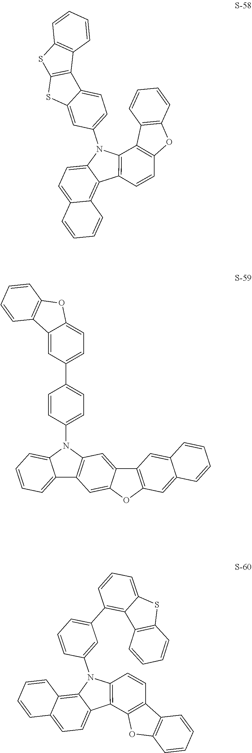
Specifically, the compound represented by Formula 5 may be represented by any one of the following compounds S-1 to S-116, but is not limited thereto.
Figure US12102004-20240924-C00088
Figure US12102004-20240924-C00089
Figure US12102004-20240924-C00090
Figure US12102004-20240924-C00091
Figure US12102004-20240924-C00092
Figure US12102004-20240924-C00093
Figure US12102004-20240924-C00094
Figure US12102004-20240924-C00095
Figure US12102004-20240924-C00096
Figure US12102004-20240924-C00097
Figure US12102004-20240924-C00098
Figure US12102004-20240924-C00099
Figure US12102004-20240924-C00100
Figure US12102004-20240924-C00101
Figure US12102004-20240924-C00102
Figure US12102004-20240924-C00103
Figure US12102004-20240924-C00104
Figure US12102004-20240924-C00105
Figure US12102004-20240924-C00106
Figure US12102004-20240924-C00107
Figure US12102004-20240924-C00108
Figure US12102004-20240924-C00109
Figure US12102004-20240924-C00110
Figure US12102004-20240924-C00111
Figure US12102004-20240924-C00112
Figure US12102004-20240924-C00113
Figure US12102004-20240924-C00114
Figure US12102004-20240924-C00115
Figure US12102004-20240924-C00116
Figure US12102004-20240924-C00117
Figure US12102004-20240924-C00118
Figure US12102004-20240924-C00119
Figure US12102004-20240924-C00120
Figure US12102004-20240924-C00121
Figure US12102004-20240924-C00122
Also, in another aspect, the present invention provides an organic electronic element comprising a first electrode; a second electrode; and an organic material layer formed between the first electrode and the second electrode; wherein the organic material layer comprises a compound represented by Formula (1) or the composition for the organic electronic element.
In another aspect, the present invention provides a method for reusing a compound of Formula (1) comprising:
    • recovering a crude organic light emitting material comprising the compound of Formula (1) of claim 1 from a deposition apparatus used in the process for depositing the organic emitting material to prepare an organic light emitting device;
    • removing impurities from the crude organic light emitting material;
    • recovering the organic light emitting material after the impurities are removed; and
    • purifying the recovered organic light emitting material to have a purity of 99.9% or higher.
The step of removing impurities from the crude organic light emitting material recovered from the deposition apparatus may preferably comprise performing a pre-purification process to obtain a purity of 98% or more by recrystallization in a recrystallization solvent.
The recrystallization solvent may be preferably a polar solvent having a polarity index (PI) of 5.5 to 7.2.
The recrystallization solvent may preferably be used by mixing a polar solvent having a polarity value of 5.5 to 7.2 and a non-polar solvent having a polarity value of 2.0 to 4.7.
When a mixture of a polar solvent and a non-polar solvent is used, the recrystallization solvent may be used in an amount of 15% (v/v) or less of the non-polar solvent compared to the polar solvent.
The recrystallization solvent may preferably be used by mixing N-Methylpyrrolidone (NMP) single solvent; or a polar solvent mixed any one selected from the group consisting of 1,3-Dimethyl-2-imidazolidinone, 2-pyrrolidone, N,N-Dimethyl formamide, Dimethyl acetamide, and Dimethyl sulfoxide to the N-Methylpyrrolidone; or alone; or mixed non-polar solvents; selected from the group consisting of Toluene, Dichloromethane (DCM), Dichloroethane (DCE), Tetrahydrofuran (THF), Chloroform, Ethyl acetate and Butanone; or a polar solvent and a non-polar solvent.
The pre-purification process may comprise a step of precipitating crystals of by cooling to 0° C. to 5° C. after dissolving the crude organic light emitting material recovered from the deposition apparatus in a polar solvent at 90° C. to 120° C.
The pre-purification process may comprise a step of precipitating crystals by cooling to 35° C. to 40° C., adding a non-polar solvent, and then cooling to 0° C. to 5° C. after dissolving the crude organic light emitting material recovered from the deposition apparatus in a polar solvent at 90° C. to 120° C.
The pre-purification process may comprise a step of precipitating crystals while concentrating the solvent and removing the non-polar solvent, after dissolving the crude organic light emitting material recovered from the deposition apparatus in a non-polar solvent.
The pre-purification process may comprise a step of recrystallizing again with a non-polar solvent after recrystallizing first with a polar solvent.
The step of purifying the recovered impurities to a purity of 99.9% or higher may comprise performing an adsorption separation process to adsorb and remove impurities by adsorbing on the adsorbent.
The adsorbent may be activated carbon, silica gel, alumina, or a material for known adsorption purposes.
The step of purifying the recovered impurities to a purity of 99.9% or higher may comprise performing sublimation purification.
Referring to FIG. 1 , the organic electronic element (100) according to the present invention comprises a first electrode (110), a second electrode (170), an organic material layer comprising single compound or 2 or more compounds represented by Formula (1) between the first electrode (110) and the second electrode (170). Wherein, the first electrode (110) may be an anode or a positive electrode, and the second electrode (170) may be a cathode or a negative electrode. In the case of an inverted organic electronic element, the first electrode may be a cathode, and the second electrode may be an anode.
The organic material layer may sequentially comprise a hole injection layer (120), a hole transport layer (130), an emitting layer (140), an electron transport layer(150), and an electron injection layer (160) formed in sequence on the first electrode(110). Here, the remaining layers except the emitting layer (140) may not be formed. The organic material layer may further comprise a hole blocking layer, an electron blocking layer, an emitting-auxiliary layer (220), a buffer layer (210), etc., and the electron transport layer (150) and the like may serve as a hole blocking layer (see FIG. 2 ).
Also, the organic electronic element according to an embodiment of the present invention may further include a protective layer or a light efficiency enhancing layer (180). The light efficiency enhancing layer may be formed on a surface not in contact with the organic material layer among both surfaces of the first electrode or on a surface not in contact with the organic material layer among both surfaces of the second electrode. The compound or materials for organic electronic element according to an embodiment of the present invention applied to the organic material layer may be used as a material for a hole injection layer (120), a hole transport layer (130), an emitting-auxiliary layer (220), an electron transport auxiliary layer, an electron transport layer (150), an electron injection layer (160), a host or dopant of an emitting layer (140), or the light efficiency enhancing layer. Preferably, for example, the composition for an organic electronic element comprising a compound represented by Formula (1) of the present invention, or a mixture of a compound represented by Formula (1) and a compound represented by Formula 4 or Formula 5 can be used as a host material for the emitting layer.
The organic material layer may include 2 or more stacks comprising a hole transport layer, an emitting layer, and an electron transport layer sequentially formed on the anode, and may further comprise a charge generation layer formed between the 2 or more stacks (see FIG. 3 ).
Otherwise, even if the same core is used, the band gap, the electrical characteristics, the interface characteristics, and the like may vary depending on which substituent is bonded at which position, therefore the choice of core and the combination of sub-substituents associated therewith is also very important, and in particular, when the optimal combination of energy levels and T1 values and unique properties of materials(mobility, interfacial characteristics, etc.) of each organic material layer is achieved, a long life span and high efficiency can be achieved at the same time.
The organic electroluminescent device according to an embodiment of the present invention may be manufactured using a PVD (physical vapor deposition) method. For example, a metal or a metal oxide having conductivity or an alloy thereof is deposited on a substrate to form a cathode, and the organic material layer including the hole injection layer(120), the hole transport layer(130), the emitting layer(140), the electron transport layer(150), and the electron injection layer(160) is formed thereon, and then depositing a material usable as a cathode thereon can manufacture an organic electroluminescent device according to an embodiment of the present invention.
Also, the present invention provides the organic electronic element wherein the organic material layer is formed by one of a spin coating process, a nozzle printing process, an inkjet printing process, a slot coating process, a dip coating process or a roll-to-roll process, and the organic material layer provides an organic electronic element comprising the compound as an electron transport material.
As another specific example, the present invention provides an organic electronic element that is used by mixing the same or different compounds of the compound represented by Formula (1) to the organic material layer. Preferably, the organic material layer comprises an emitting layer, wherein the emitting layer comprises a composition for an organic electronic element comprising a compound represented by Formula (1) or a mixture of a compound represented by Formula (1) and a compound represented by Formula 4 or Formula 5.
Also, the present invention provides a composition for an organic electronic element comprising a compound represented by Formula (1), or a mixture of a compound represented by Formula (1) and a compound represented by Formula 4 or Formula 5, and provides an organic electronic element comprising the composition.
Also, the present invention also provides an electronic device comprising a display device comprising the organic electronic element; and a control unit for driving the display device.
According to another aspect, the present invention provides an electronic device wherein the organic electronic element is at least one of an OLED, an organic solar cell, an organic photo conductor, an organic transistor (organic TFT) and an element for monochromic or white illumination. Wherein, the electronic device may be a wired/wireless communication terminal which is currently used or will be used in the future, and covers all kinds of electronic devices including a mobile communication terminal such as a cellular phone, a personal digital assistant(PDA), an electronic dictionary, a point-to-multipoint(PMP), a remote controller, a navigation unit, a game player, various kinds of TVs, and various kinds of computers.
Hereinafter, Synthesis examples of the compound represented by Formula (1), Formula 4 and Formula 5 of the present invention and preparation examples of the organic electronic element of the present invention will be described in detail by way of example, but are not limited to the following examples.
SYNTHESIS EXAMPLE
The compound (final products) represented by Formula (1) according to the present invention is synthesized by reacting Sub1 and Sub 2 as shown in Reaction Scheme 1, but is not limited thereto.
Reaction Scheme 1
Figure US12102004-20240924-C00123
Wherein, R1, R2, R3, L1, L2, Ar1, Ar2, a, b and c are the same as defined in Formula 1.
I. Synthesis of Final Product
1. Synthesis Example of P-1
Figure US12102004-20240924-C00124
Sub1-1 (20.00 g, 49.22 mmol), Sub2-1 (22.05 g, 49.22 mmol), Pd(PPh3)4 (1.71 g, 1.48 mmol), NaOH (3.94 g, 98.44 mmol), THF (164 mL) and water (55 mL) were added to the round bottom flask, and reacted at 75° C. for 8 hours. When the reaction is completed, the temperature of the reactant is cooled to room temperature and the reaction solvent is removed. The concentrated reactant was recrystallized using a silicagel column to obtain 26.56 g (78%) of product P-1.
2. Synthesis Example of P-15
Figure US12102004-20240924-C00125
Sub1-1 (21.00 g, 51.68 mmol), Sub2-7 (23.25 g, 51.68 mmol), Pd(PPh3)4 (1.79 g, 1.55 mmol), NaOH (4.13 g, 103.36 mmol), THF (172 mL) and water (57 mL) were added to the round bottom flask, and reacted at 75° C. for 8 hours. When the reaction is completed, the temperature of the reactant is cooled to room temperature and the reaction solvent is removed. The concentrated reactant was recrystallized using a silicagel column to obtain 22.95 g (64%) of product P-15.
3. Synthesis Example of P-17
Figure US12102004-20240924-C00126
Sub1-2 (17.00 g, 41.33 mmol), Sub2-9 (17.93 g, 41.33 mmol), Pd(PPh3)4 (1.43 g, 1.24 mmol), NaOH (3.31 g, 82.65 mmol), and THF (138 mL) and water (46 mL) were added to the round bottom flask, and reacted at 75° C. for 8 hours. When the reaction is completed, the temperature of the reactant is cooled to room temperature and the reaction solvent is removed. The concentrated reactant was recrystallized using a silicagel column to obtain 20.60 g (73%) of product P-17.
4. Synthesis Example of P-27
Figure US12102004-20240924-C00127
Sub1-1 (19.00 g, 46.76 mmol), Sub2-11 (24.60 g, 46.76 mmol), Pd(PPh3)4 (1.62 g, 1.40 mmol), NaOH (3.74 g, 93.52 mmol), and THF (156 mL) and water (32 mL) were added to the round bottom flask, and reacted at 75° C. for 8 hours. When the reaction is completed, the temperature of the reactant is cooled to room temperature and the reaction solvent is removed. The concentrated reactant was recrystallized using a silicagel column to obtain 25.56 g (71%) of product P-27.
5. Synthesis Example of P-44
Figure US12102004-20240924-C00128
Sub1-1 (30.00 g, 73.83 mmol), Sub2-4 (32.33 g, 73.83 mmol), Pd(PPh3)4 (2.56 g, 2.21 mmol), NaOH (5.91 g, 147.66 mmol), THF (246 mL) and water (82 mL) were added to the round bottom flask, and reacted at 75° C. for 8 hours. When the reaction is completed, the temperature of the reactant is cooled to room temperature and the reaction solvent is removed. The concentrated reactant was recrystallized using a silicagel column to obtain 31.21 g (62%) of product P-44.
6. Synthesis Example of P-49
Figure US12102004-20240924-C00129
Sub1-2 (25.00 g, 60.77 mmol), Sub2-17 (22.78 g, 60.77 mmol), Pd(PPh3)4 (2.11 g, 1.82 mmol), NaOH (4.86 g, 121.55 mmol), THF (203 mL) and water (68 mL) were added to the round bottom flask, and reacted at 75° C. for 8 hours. When the reaction is completed, the temperature of the reactant is cooled to room temperature and the reaction solvent is removed. The concentrated reactant was recrystallized using a silicagel column to obtain 28.43 g (75%) of product P-49.
7. Synthesis Example of P-55
Figure US12102004-20240924-C00130

1) Synthesis of Sub 1-4c
Sub1-4a (19.83 g, 123.60 mmol), Sub1-4b (35.00 g, 123.60 mmol), Pd(PPh3)4 (4.29 g, 3.71 mmol), K2CO3 (34.17 g, 247.20 mmol) were added to a round bottom flask, dissolved in anhydrous THF (412 mL) and water (137 mL), and then refluxed for 12 hours. When the reaction was completed, the temperature of the reactant was cooled to room temperature, extracted with CH2Cl2 and water, and then treated with MgSO4. The product produced by concentrating the organic solvent was recrystallized using a silicagel column to obtain 34.68 g (88%) of Sub1-4c.
2) Synthesis of Sub 1-4
Sub1-4c (34.00 g, 106.64 mmol), 4,4,4′,4′,5,5,5′,5′-octamethyl-2,2′-bi(1,3,2-dioxaborolane) (35.20 g, 138.63 mmol), Pd2(dba)3 (2.93 g, 3.20 mmol), Xphos (3.05 g, 6.40 mmol), KOAc (20.93 g, 213.27 mmol) were added to Toluene (355 mL) and stirred at 120° C. for 2 hours. When the reaction was completed, the reaction solvent was removed and the concentrated organic material was recrystallized using a silicagel column to obtain 25.82 g (59%) of product Sub1-4.
3) Synthesis of P-55
Sub1-4 (15.00 g, 36.55 mmol), Sub2-14 (14.58 g, 36.55 mmol), Pd(PPh3)4 (1.27 g, 1.10 mmol), NaOH (2.92 g, 73.11 mmol) and THF (121 mL) and water (40 mL) were added to the round bottom flask, and reacted at 75° C. for 8 hours. When the reaction is completed, the temperature of the reactant is cooled to room temperature and the reaction solvent is removed. The concentrated reactant was recrystallized using a silicagel column to obtain 16.55 g (70%) of product P-55.
8. Synthesis Example of P-73
Figure US12102004-20240924-C00131
Sub1-1 (16.00 g, 39.38 mmol), Sub2-21 (15.71 g, 39.38 mmol), Pd(PPh3)4 (1.37 g, 1.18 mmol), NaOH (3.15 g, 78.75 mmol) and THF (132 mL) and water (44 mL) were added to the round bottom flask, and reacted at 75° C. for 8 hours. When the reaction is completed, the temperature of the reactant is cooled to room temperature and the reaction solvent is removed. The concentrated reactant was recrystallized using a silicagel column to obtain 18.22 g (72%) of product P-73.
9. Synthesis Example of P-91
Figure US12102004-20240924-C00132
Sub1-1 (21.00 g, 51.68 mmol), Sub2-20 (23.15 g, 51.68 mmol), Pd(PPh3)4 (1.79 g, 1.55 mmol), NaOH (4.13 g, 103.36 mmol) and THF (172 mL) and water (58 mL) were added to the round bottom flask, and reacted at 75° C. for 8 hours. When the reaction is completed, the temperature of the reactant is cooled to room temperature and the reaction solvent is removed. The concentrated reactant was recrystallized using a silicagel column to obtain 23.24 g (65%) of product P-91.
Sub 1 in Reaction Scheme 1 may be the following compound, but is not limited thereto, and the FD-MS (Field Desorption-Mass Spectrometry) values of the compounds belonging to Sub 1 are shown in Table 1.
Figure US12102004-20240924-C00133
Figure US12102004-20240924-C00134
TABLE 1
Compound FD-MS compound FD-MS
Sub1-1 m/z = 406.21(C28H27BO2 = 406.33) Sub1-2 m/z = 411.24(C28H22D5BO2 = 411.36)
Sub1-3 m/z = 412.25(C28H21D6BO2 = 412.37) Sub1-4 m/z = 410.24(C28H23D4BO2 = 410.36)
Sub1-5 m/z = 415.27(C28H18D9BO2 = 415.39) Sub1-6 m/z = 416.27(C28H17D10BO2 = 416.39)
Sub1-7 m/z = 417.28(C28H16D11BO2 = 417.4) Sub1-8 m/z = 421.3(C28H12D15BO2 = 421.42)
Sub 2 in Reaction Scheme 1 may be the following compound, but is not limited thereto, and the FD-MS (Field Desorption-Mass Spectrometry) values of the compounds belonging to Sub 2 are shown in Table 2.
Figure US12102004-20240924-C00135
Figure US12102004-20240924-C00136
Figure US12102004-20240924-C00137
Figure US12102004-20240924-C00138
Figure US12102004-20240924-C00139
Figure US12102004-20240924-C00140
TABLE 2
Compound FD-MS Compound FD-MS
Sub2-1 m/z = 447.08(C27H14ClN3O2 = 447.88) Sub2-2 m/z = 539.09(C33H18ClN3OS = 540.04)
Sub2-3 m/z = 490.16(C31H11D7ClN3O = 491) Sub2-4 m/z = 437.08(C26H16ClN3S = 437.95)
Sub2-5 m/z = 407.08(C25H14ClN3O = 407.86) Sub2-6 m/z = 509.13(C33H20ClN3O = 509.99)
Sub2-7 m/z = 449.08(C27H16ClN3S = 449.96) Sub2-8 m/z = 430.1(C25H7D7ClN3S = 430.96)
Sub2-9 m/z = 433.1(C27H16ClN3O = 433.9) Sub2-10 m/z = 509.13(C33H20ClN3O = 509.99)
Sub2-11 m/z = 525.11(C33H20ClN3S = 526.05) Sub2-12 m/z = 439.14(C27H10D6ClN3O = 439.93)
Sub2-13 m/z = 407.08(C25H14ClN3O = 407.86) Sub2-14 m/z = 398.13(C25H11D5ClN3 = 398.9)
Sub2-15 m/z = 398.13(C25H11D5ClN3 = 398.9) Sub2-16 m/z = 463.05(C27H14ClN3OS = 463.94)
Sub2-17 m/z = 374.13(C23H7D7ClN3 = 374.88) Sub2-18 m/z = 469.13(C31H20ClN3 = 469.97)
Sub2-19 m/z = 669.14(C43H25ClFN3S = 670.2) Sub2-20 m/z = 447.11(C28H18ClN3O = 447.92)
Sub2-21 m/z = 398.13(C25H11D5ClN3 = 398.9) Sub2-22 m/z = 367.09(C23H14ClN3 = 367.84)
Sub2-23 m/z = 367.09(C23H14ClN3 = 367.84) Sub2-24 m/z = 425.17(C27H24ClN3 = 425.96)
The FD-MS (Field Desorption-Mass Spectrometry) values of compounds P-1 to P-96 of the present invention prepared according to the above synthesis examples are shown in Table 3.
TABLE 3
Compound FD-MS Compound FD-MS
P-1 m/z = 691.23(C49H29N3O2 = 691.79) P-2 m/z = 783.23(C55H33N3OS = 783.95)
P-3 m/z = 707.2(C49H29N3OS = 707.85) P-4 m/z = 783.23(C55H33N3OS = 783.95)
P-5 m/z = 727.26(C53H33N3O = 727.87) P-6 m/z = 734.31(C53H26D7N3O = 734.91)
P-7 m/z = 757.3(C55H31D4N3O = 757.93) P-8 m/z = 707.2(C49H29N3OS = 707.85)
P-9 m/z = 601.22(C43H27N3O = 601.71) P-10 m/z = 657.27(C47H23D6N3O = 657.81)
P-11 m/z = 677.25(C49H31N3O = 677.81) P-12 m/z = 753.28(C55H35N3O = 753.9)
P-13 m/z = 617.19(C43H27N3S = 617.77) P-14 m/z = 728.29(C51H20D11N3S = 728.96)
P-15 m/z = 693.22(C49H31N3S = 693.87) P-16 m/z = 674.25(C47H22D7N3S = 674.87)
P-17 m/z = 682.28(C49H26D5N3O = 682.84) P-18 m/z = 727.26(C53H33N3O = 727.87)
P-19 m/z = 683.28(C49H25D6N3O = 683.84) P-20 m/z = 677.25(C49H31N3O = 677.81)
P-21 m/z = 698.26(C49H26D5N3S = 698.9) P-22 m/z = 743.24(C53H33N3S = 743.93)
P-23 m/z = 693.22(C49H31N3S = 693.87) P-24 m/z = 693.22(C49H31N3S = 693.87)
P-25 m/z = 753.28(C55H35N3O = 753.9) P-26 m/z = 727.26(C53H33N3O = 727.87)
P-27 m/z = 769.26(C55H35N3S = 769.97) P-28 m/z = 697.25(C49H27D4N3S = 697.89)
P-29 m/z = 727.26(C53H33N3O = 727.87) P-30 m/z = 733.3(C53H27D6N3O = 733.9)
P-31 m/z = 743.24(C53H33N3S = 743.93) P-32 m/z = 769.26(C55H35N3S = 769.97)
P-33 m/z = 667.21(C47H29N3S = 667.83) P-34 m/z = 660.29(C47H20D9N3O = 660.82)
P-35 m/z = 701.25(C51H31N3O = 701.83) P-36 m/z = 651.23(C47H29N3O = 651.77)
P-37 m/z = 677.25(C49H31N3O = 677.81) P-38 m/z = 727.26(C53H33N3O = 727.87)
P-39 m/z = 743.24(C53H33N3S = 743.93) P-40 m/z = 769.26(C55H35N3S = 769.97)
P-41 m/z = 651.23(C47H29N3O = 651.77) P-42 m/z = 743.24(C53H33N3S = 743.93)
P-43 m/z = 717.22(C51H31N3S = 717.89) P-44 m/z = 681.22(C48H31N3S = 681.86)
P-45 m/z = 511.2(C37H25N3 = 511.63) P-46 m/z = 561.22(C41H27N3 = 561.69)
P-47 m/z = 561.22(C41H27N3 = 561.69) P-48 m/z = 620.29(C45H20D9N3 = 620.8)
P-49 m/z = 623.31(C45H17D12N3 = 623.82) P-50 m/z = 626.33(C45H14D15N3 = 626.84)
P-51 m/z = 611.24(C45H29N3 = 611.75) P-52 m/z = 661.25(C49H31N3 = 661.81)
P-53 m/z = 663.27(C49H33N3 = 663.82) P-54 m/z = 646.31(C47H22D9N3 = 646.84)
P-55 m/z = 646.31(C47H22D9N3 = 646.84) P-56 m/z = 587.24(C43H29N3 = 587.73)
P-57 m/z = 637.25(C47H31N3 = 637.79) P-58 m/z = 642.28(C47H26D5N3 = 642.82)
P-59 m/z = 611.24(C45H29N3 = 611.75) P-60 m/z = 643.29(C47H25D6N3 = 643.82)
P-61 m/z = 713.28(C53H35N3 = 713.88) P-62 m/z = 687.27(C51H33N3 = 687.85)
P-63 m/z = 694.31(C51H26D7N3 = 694.89) P-64 m/z = 637.25(C47H31N3 = 637.79)
P-65 m/z = 687.27(C51H33N3 = 687.85) P-66 m/z = 611.24(C45H29N3 = 611.75)
P-67 m/z = 637.25(C47H31N3 = 637.79) P-68 m/z = 687.27(C51H33N3 = 687.85)
P-69 m/z = 637.25(C47H31N3 = 637.79) P-70 m/z = 642.28(C47H26D5N3 = 642.82)
P-71 m/z = 687.27(C51H33N3 = 687.85) P-72 m/z = 687.27(C51H33N3 = 687.85)
P-73 m/z = 642.28(C47H26D5N3 = 642.82) P-74 m/z = 637.25(C47H31N3 = 637.79)
P-75 m/z = 713.28(C53H35N3 = 713.88) P-76 m/z = 687.27(C51H33N3 = 687.85)
P-77 m/z = 687.27(C51H33N3 = 687.85) P-78 m/z = 687.27(C51H33N3 = 687.85)
P-79 m/z = 661.25(C49H31N3 = 661.81) P-80 m/z = 663.27(C49H33N3 = 663.82)
P-81 m/z = 713.28(C53H35N3 = 713.88) P-82 m/z = 713.28(C53H35N3 = 713.88)
P-83 m/z = 797.34(C58H43N3O = 798) P-84 m/z = 913.29(C65H40FN3S = 914.11)
P-85 m/z = 761.23(C53H32FN3S = 761.92) P-86 m/z = 795.36(C59H45N3 = 796.03)
P-87 m/z = 812.3(C58H32D5N3S = 813.05) P-88 m/z = 729.31(C54H39N3 = 729.93)
P-89 m/z = 845.29(C61H39N3S = 846.06) P-90 m/z = 673.34(C49H35D4N3 = 673.9)
P-91 m/z = 691.26(C50H33N3O = 691.83) P-92 m/z = 738.28(C54H34N4 = 738.89)
P-93 m/z = 713.28(C53H35N3 = 713.88) P-94 m/z = 795.36(C59H45N3 = 796.03)
P-95 m/z = 769.26(C55H35N3S = 769.97) P-96 m/z = 667.29(C49H29D4N3 = 667.85)
Compounds represented by Formula 4 or Formula 5 may be prepared by referring to known synthetic methods (named reactions) or published patent publications, for example, Korean Patent Registration No. 10-2395819, U.S. Patent Publication No. 2023-0129535, etc., but are not limited thereto.
Meanwhile, the FD-MS values of the compounds H-1 to H-124 and S-1 to S-116 of the present invention are shown in Tables 4 and 5.
TABLE 4
Compound FD-MS Compound FD-MS
H-1 m/z = 487.19(C36H25NO = 487.6) H-2 m/z = 553.19(C40H27NS = 553.72)
H-3 m/z = 563.26(C43H33N = 563.74) H-4 m/z = 602.27(C45H34N2 = 602.78)
H-5 m/z = 517.15(C36H23NOS = 517.65) H-6 m/z = 603.2(C44H29NS = 603.78)
H-7 m/z = 735.29(C57H37N = 735.93) H-8 m/z = 562.24(C42H30N2 = 562.72)
H-9 m/z = 565.17(C40H23NO3 = 565.63) H-10 m/z = 581.14(C40H23NO2S = 581.69)
H-11 m/z = 823.24(C59H37NS2 = 824.07) H-12 m/z = 727.3(C54H37N3 = 727.91)
H-13 m/z = 627.22(C46H29NO2 = 627.74) H-14 m/z = 633.16(C44H27NS2 = 633.83)
H-15 m/z = 675.29(C52H37N = 675.88) H-16 m/z = 678.3(C51H38N2 = 678.88)
H-17 m/z = 669.21(C48H31NOS = 669.84) H-18 m/z = 785.22(C56H35NS2 = 786.02)
H-19 m/z = 617.18(C44H27NOS = 617.77) H-20 m/z = 601.2(C44H27NO2 = 601.71)
H-21 m/z = 779.32(C59H41NO = 779.98) H-22 m/z = 583.23(C42H33NS = 583.79)
H-23 m/z = 679.32(C52H41N = 679.91) H-24 m/z = 726.27(C54H34N2O = 726.88)
H-25 m/z = 593.18(C42H27NOS = 593.74) H-26 m/z = 774.22(C54H34N2S2 = 775)
H-27 m/z = 557.24(C40H31NO2 = 557.69) H-28 m/z = 652.25(C48H32N2O = 652.8)
H-29 m/z = 619.29(C46H37NO = 619.81) H-30 m/z = 603.2(C44H29NS = 603.78)
H-31 m/z = 813.3(C62H39NO = 814) H-32 m/z = 784.29(C57H40N2S = 785.02)
H-33 m/z = 577.2(C42H27NO2 = 577.68) H-34 m/z = 607.14(C42H25NS2 = 607.79)
H-35 m/z = 801.34(C62H43N = 802.03) H-36 m/z = 575.24(C42H29N3 = 575.72)
H-37 m/z = 577.2(C42H27NO2 = 577.68) H-38 m/z = 607.14(C42H25NS2 = 607.79)
H-39 m/z = 801.34(C62H43N = 802.03) H-40 m/z = 575.24(C42H29N3 = 575.72)
H-41 m/z = 601.2(C44H27NO2 = 601.71) H-42 m/z = 471.11(C31H21NS2 = 471.64)
H-43 m/z = 675.29(C52H37N = 675.88) H-44 m/z = 727.3(C54H37N3 = 727.91)
H-45 m/z = 603.2(C44H29NS = 603.78) H-46 m/z = 561.16(C38H27NS2 = 561.76)
H-47 m/z = 799.32(C62H41N = 800.02) H-48 m/z = 702.27(C52H34N2O = 702.86)
H-49 m/z = 729.27(C54H35NO2 = 729.88) H-50 m/z = 785.22(C56H35NS2 = 786.02)
H-51 m/z = 812.32(C62H40N2 = 813.02) H-52 m/z = 681.22(C48H31N3S = 681.86)
H-53 m/z = 615.18(C44H25NO3 = 615.69) H-54 m/z = 763.15(C52H29NS3 = 763.99)
H-55 m/z = 593.31(C45H39N = 593.81) H-56 m/z = 840.33(C62H40N4 = 841.03)
H-57 m/z = 657.18(C46H27NO2S = 657.79) H-58 m/z = 824.23(C58H36N2S2 = 825.06)
H-59 m/z = 1195.42(C91H57NS = 1196.52) H-60 m/z = 656.19(C46H28N2OS = 656.8)
H-61 m/z = 607.16(C42H25NO2S = 607.73) H-62 m/z = 773.2(C54H31NO3S = 773.91)
H-63 m/z = 1013.4(C79H51N = 1014.28) H-64 m/z = 758.24(C54H34N2OS = 758.94)
H-65 m/z = 623.14(C42H25NOS2 = 623.79) H-66 m/z = 763.16(C52H29NO2S2 = 763.93)
H-67 m/z = 799.2(C56H33NOS2 = 800.01) H-68 m/z = 743.23(C54H33NOS = 743.92)
H-69 m/z = 872.25(C62H36N2O2S = 873.04) H-70 m/z = 772.22(C54H32N2O2S = 772.92)
H-71 m/z = 830.28(C61H38N2S = 831.05) H-72 m/z = 808.25(C58H33FN2O2 = 808.91)
H-73 m/z = 929.21(C64H35NO3S2 = 930.11) H-74 m/z = 963.27(C68H41N3S2 = 964.22)
H-75 m/z = 809.24(C58H35NO2S = 809.98) H-76 m/z = 893.29(C66H39NO3 = 894.04)
H-77 m/z = 794.28(C58H38N2S = 795.02) H-78 m/z = 900.26(C64H40N2S2 = 901.16)
H-79 m/z = 758.28(C55H38N2S = 758.98) H-80 m/z = 1082.37(C81H50N2S = 1083.37)
H-81 m/z = 573.25(C44H31N = 573.74) H-82 m/z = 649.28(C50H35N = 649.84)
H-83 m/z = 699.29(C54H37N = 699.9) H-84 m/z = 699.29(C54H37N = 699.9)
H-85 m/z = 673.28(C52H35N = 673.86) H-86 m/z = 649.28(C50H35N = 649.84)
H-87 m/z = 625.28(C48H35N = 625.82) H-88 m/z = 673.28(C52H35N = 673.86)
H-89 m/z = 773.31(C60H39N = 773.98) H-90 m/z = 749.31(C58H39N = 749.96)
H-91 m/z = 699.29(C54H37N = 699.9) H-92 m/z = 599.26(C46H33N = 599.78)
H-93 m/z = 639.26(C48H33NO = 639.8) H-94 m/z = 765.25(C57H35NS = 765.97)
H-95 m/z = 677.31(C52H39N = 677.89) H-96 m/z = 727.3(C54H37N3 = 727.91)
H-97 m/z = 552.18(C39H24N2O2 = 552.63) H-98 m/z = 628.22(C45H28N2O2 = 628.73)
H-99 m/z = 614.24(C45H30N2O = 614.75) H-100 m/z = 614.24(C45H30N2O = 614.75)
H-101 m/z = 691.21(C50H29NO3 = 691.79) H-102 m/z = 739.29(C56H37NO = 739.92)
H-103 m/z = 673.15(C46H27NOS2 = 673.85) H-104 m/z = 726.27(C54H34N2O = 726.88)
H-105 m/z = 617.18(C44H27NOS = 617.77) H-106 m/z = 611.22(C46H29NO = 611.74)
H-107 m/z = 769.24(C56H35NOS = 769.96) H-108 m/z = 701.28(C52H35N3 = 701.87)
H-109 m/z = 527.22(C39H29NO = 527.67) H-110 m/z = 643.2(C46H29NOS = 643.8)
H-111 m/z = 593.18(C42H27NOS = 593.74) H-112 m/z = 726.27(C54H34N2O = 726.88)
H-113 m/z = 726.27(C54H34N2O = 726.88) H-114 m/z = 558.14(C37H22N2O2S = 558.65)
H-115 m/z = 620.19(C43H28N2OS = 620.77) H-116 m/z = 686.27(C52H34N2 = 686.86)
H-117 m/z = 718.24(C52H34N2S = 718.92) H-118 m/z = 728.28(C54H36N2O = 728.89)
H-119 m/z = 592.2(C42H28N2S = 592.76) H-120 m/z = 756.22(C54H32N2OS = 756.92)
H-121 m/z = 547.70(C42H29N = 547.70) H-122 m/z = 672.28(C49H24D7NO2 = 672.83)
H-123 m/z = 626.28(C48H26D5N = 558.75) H-124 m/z = 558.22(C40H22D5NS = 558.75)
TABLE 5
Compound FD-MS Compound FD-MS
S-1 m/z = 408.16(C30H20N2 = 408.5) S-2 m/z = 534.21(C40H26N2 = 534.66)
S-3 m/z = 560.23(C42H28N2 = 560.7) S-4 m/z = 584.23(C44H28N2 = 584.72)
S-5 m/z = 560.23(C42H28N2 = 560.7) S-6 m/z = 634.24(C48H30N2 = 634.78)
S-7 m/z = 610.24(C46H30N2 = 610.76) S-8 m/z = 498.17(C36H22N2O = 498.59)
S-9 m/z = 574.2(C42H26N2O = 574.68) S-10 m/z = 660.26(C50H32N2 = 660.82)
S-11 m/z = 686.27(C52H34N2 = 686.86) S-12 m/z = 620.14(C42H24N2S2 = 620.79)
S-13 m/z = 640.2(C46H28N2S = 640.8) S-14 m/z = 560.23(C42H28N2 = 560.7)
S-15 m/z = 558.21(C42H26N2 = 558.68) S-16 m/z = 548.19(C40H24N2O = 548.65)
S-17 m/z = 573.22(C42H27N3 = 573.7) S-18 m/z = 564.17(C40H24N2S = 564.71)
S-19 m/z = 574.2(C42H26N2O = 574.68) S-20 m/z = 564.17(C40H24N2S = 564.71)
S-21 m/z = 564.17(C40H24N2S = 564.71) S-22 m/z = 813.31(C61H39N3 = 814)
S-23 m/z = 696.26(C53H32N2 = 696.85) S-24 m/z = 691.23(C49H29N3O2 = 691.79)
S-25 m/z = 710.27(C54H34N2 = 710.88) S-26 m/z = 610.24(C46H30N2 = 610.76)
S-27 m/z = 670.15(C46H26N2S2 = 670.85) S-28 m/z = 640.29(C48H36N2 = 640.83)
S-29 m/z = 598.2(C44H26N2O = 598.71) S-30 m/z = 623.24(C46H29N3 = 623.76)
S-31 m/z = 458.18(C34H22N2 = 458.56) S-32 m/z = 548.19(C40H24N2O = 548.65)
S-33 m/z = 508.19(C38H24N2 = 508.62) S-34 m/z = 508.19(C38H24N2 = 508.62)
S-35 m/z = 623.24(C46H29N3 = 623.76) S-36 m/z = 564.17(C40H24N2S = 564.71)
S-37 m/z = 627.2(C46H29NS = 627.81) S-38 m/z = 505.1(C34H19NS2 = 505.65)
S-39 m/z = 514.15(C36H22N2S = 514.65) S-40 m/z = 575.17(C42H25NS = 575.73)
S-41 m/z = 642.21(C46H30N2S = 642.82) S-42 m/z = 575.17(C42H25NS = 575.73)
S-43 m/z = 606.18(C42H26N2OS = 606.74) S-44 m/z = 575.17(C42H25NS = 575.73)
S-45 m/z = 551.17(C40H25NS = 551.71) S-46 m/z = 607.14(C42H25NS2 = 607.79)
S-47 m/z = 525.16(C38H23NS = 525.67) S-48 m/z = 642.21(C46H30N2S = 642.82)
S-49 m/z = 548.19(C40H24N2O = 548.65) S-50 m/z = 473.14(C34H19NO2 = 473.53)
S-51 m/z = 566.15(C39H22N2OS = 566.68) S-52 m/z = 459.16(C34H21NO = 459.55)
S-53 m/z = 473.14(C34H19NO2 = 473.53) S-54 m/z = 523.16(C38H21NO2 = 523.59)
S-55 m/z = 539.13(C38H21NOS = 539.65) S-56 m/z = 548.19(C40H24N2O = 548.65)
S-57 m/z = 489.12(C34H19NOS = 489.59) S-58 m/z = 545.09(C36H19NOS2 = 545.67)
S-59 m/z = 549.17(C40H23NO2 = 549.63) S-60 m/z = 565.15(C40H23NOS = 565.69)
S-61 m/z = 523.16(C38H21NO2 = 523.59) S-62 m/z = 598.2(C44H26N2O = 598.71)
S-63 m/z = 539.13(C38H21NOS = 539.65) S-64 m/z = 589.15(C42H23NOS = 589.71)
S-65 m/z = 498.17(C36H22N2O = 498.59) S-66 m/z = 509.18(C38H23NO = 509.61)
S-67 m/z = 548.19(C40H24N2O = 548.65) S-68 m/z = 549.17(C40H23NO2 = 549.63)
S-69 m/z = 449.12(C32H19NS = 449.57) S-70 m/z = 439.1(C30H17NOS = 439.53)
S-71 m/z = 647.22(C49H29NO = 647.78) S-72 m/z = 717.28(C52H35N3O = 717.87)
S-73 m/z = 459.16(C34H21NO = 459.55) S-74 m/z = 533.18(C40H23NO = 533.63)
S-75 m/z = 525.16(C38H23NS = 525.67) S-76 m/z = 564.17(C40H24N2S = 564.71)
S-77 m/z = 575.19(C42H25NO2 = 575.67) S-78 m/z = 663.22(C49H29NO2 = 663.78)
S-79 m/z = 647.22(C49H29NO = 647.78) S-80 m/z = 496.16(C36H20N2O = 496.57)
S-81 m/z = 565.15(C40H23NOS = 565.69) S-82 m/z = 505.1(C34H19NS2 = 505.65)
S-83 m/z = 765.25(C56H35NOSi = 765.99) S-84 m/z = 615.17(C44H25NOS = 615.75)
S-85 m/z = 603.17(C43H25NOS = 603.74) S-86 m/z = 772.29(C59H36N2 = 772.95)
S-87 m/z = 802.33(C61H42N2 = 803.02) S-88 m/z = 607.23(C47H29N = 607.76)
S-89 m/z = 524.23(C39H28N2 = 524.67) S-90 m/z = 665.22(C49H31NS = 665.85)
S-91 m/z = 633.25(C49H31N = 633.79) S-92 m/z = 775.29(C59H37NO = 775.95)
S-93 m/z = 535.23(C41H29N = 535.69) S-94 m/z = 623.22(C47H29NO = 623.76)
S-95 m/z = 687.2(C51H29NS = 687.86) S-96 m/z = 735.29(C57H37N = 735.93)
S-97 m/z = 611.26(C47H33N = 611.79) S-98 m/z = 679.23(C50H33NS = 679.88)
S-99 m/z = 787.32(C61H41N = 788.01) S-100 m/z = 743.33(C55H41N3 = 743.95)
S-101 m/z = 485.21(C37H27N = 485.63) S-102 m/z = 471.2(C36H25N = 471.6)
S-103 m/z = 571.19(C43H25NO = 571.68) S-104 m/z = 584.23(C44H28N2 = 584.72)
S-105 m/z = 539.24(C40H21D5N2 = 539.69) S-106 m/z = 453.15(C32H15NS = 471.6)
S-107 m/z = 563.26(C43H26D4NO = 563.74) S-108 m/z = 589.26(C44H23D5N2 = 584.72)
S-109 m/z = 589.26(C44H23D5N2 = 589.75) S-110 m/z = 562.23(C42H22D4N2 = 562.71)
S-111 m/z = 660.26(C50H32N2 = 660.82) S-112 m/z = 553.22(C40H19D5N2O = 553.68)
S-113 m/z = 634.24(C48H30N2 = 634.78) S-114 m/z = 589.26(C44H23D5N2 = 589.75)
S-115 m/z = 588.25(C44H24D4N2 = 588.75) S-116 m/z = 513.23(C38H19D5N2 = 513.65)
Meanwhile, exemplary synthesis examples of the present invention represented by Formula (1), Formula 4, and Formula 5 have been described, but these are all based on the Buchwald-Hartwig cross coupling reaction, Miyaura boration reaction, Suzuki cross-coupling reaction, Intramolecular acid-induced cyclization reaction (J. mater. Chem. 1999, 9, 2095.), Pd(II)-catalyzed oxidative cyclization reaction (Org. Lett. 2011, 13, 5504), and PPh3-mediated reductive cyclization reaction (J. Org. Chem. 2005, 70, 5014.), and it will be easily understood by those skilled in the art that the reaction proceeds even when other substituents defined in Formula (1), Formula 4, or Formula 5 are bonded in addition to the substituents specified in the specific synthesis examples.
Manufacturing Evaluation of Organic Electronic Elements
Example 1 Red Organic Light Emitting Device (Phosphorescent Host)
Compound A and Compound B were used on the ITO layer (anode) formed on a glass substrate, and a hole injection layer with a thickness of 10 nm was formed by doping Compound B at a weight ratio of 98:2, and then Compound A was vacuum deposited on the hole injection layer to a thickness of 110 nm to form a hole transport layer. Next, Compound C-R was vacuum deposited to a thickness of 10 nm on the hole transport layer to form an emitting-auxiliary layer. Thereafter, the host material of the emitting layer uses Compound P-1, a compound of the present invention, as the first host, and Compound H-20, a compound of the present invention, as the second host, and a mixture of the first host and the second host in a weight ratio of 5:5 is used, and bis-(1-phenylisoquinolyl)iridium(III)acetylacetonate (hereinafter abbreviated as ‘(piq)2Ir(acac)’) was used as a dopant material, and an emitting layer with a thickness of 30 nm was formed by doping the dopant so that the weight ratio of the host and the dopant was 95:5.
Next, Compound E is vacuum deposited on the emitting layer to form a hole blocking layer with a thickness of 10 nm, and an electron transport layer with a thickness of 30 nm was formed on the hole blocking layer using a mixture of Compound F and Compound G at a weight ratio of 5:5. Afterwards, Compound G was deposited on the electron transport layer to form an electron injection layer with a thickness of 0.2 nm, and then Al was deposited to form a cathode with a thickness of 150 nm.
Compound A: N-([1,1′-biphenyl]-4-yl)-9,9-dimethyl-N-(4-(9-phenyl-9H-carbazol-3-yl)phenyl)-9H-fluoren-2-amine
Compound B: 4,4′,4″-((1E,1′E,1″E)-cyclopropane-1,2,3-triylidenetris(cyanomethaneylylidene))tris(2,3,5,6-tetrafluorobenzonitrile)
Compound C-R: N7-(dibenzo[b,d]thiophen-2-yl)-N2,N2,N7-triphenyldibenzo[b,d]thiophene-2,7-diamine
Compound E: 2-(4′-(9,9-dimethyl-9H-fluoren-2-yl)-[1,1′-biphenyl]-3-yl)-4,6-diphenyl-1,3,5-triazine
Compound F: 2,7-bis(4-(4,6-diphenyl-1,3,5-triazin-2-yl)phenyl)naphthalene
Compound G: (8-quinolinolato)lithium
Example 2 to Example 36
An organic light emitting device was manufactured in the same manner as in Example 1, except that the compound of the present invention described in Table 6 was used as the host material of the emitting layer.
Comparative Example 1 and Comparative Example 2
An organic light emitting device was manufactured in the same manner as in Example 1, except that Comparative Compound A and Comparative Compound B were used as the first host as the host material of the emitting layer.
Figure US12102004-20240924-C00141
To the organic electroluminescent device manufactured by Examples 1 to 36, Comparative Example 1 and Comparative Example 2 of the present invention, Electroluminescence (EL) characteristics were measured with a PR-650 of Photoresearch Co., by applying a forward bias DC voltage. As a result of the measurement, T95 life was measured at a standard luminance of 2,500 cd/m2 through life measuring apparatus manufactured by McScience. Table 6 shows the results of element fabrication and evaluation.
The measuring apparatus can evaluate the performance of new materials compared to comparative compounds under identical conditions, without being affected by possible daily fluctuations in deposition rate, vacuum quality or other parameters.
During the evaluation, one batch contains 4 identically prepared OLEDs including a comparative compound, and the performance of a total of 12 OLEDs is evaluated in 3 batches, so the value of the experimental results obtained in this way indicates statistical significance.
TABLE 6
Current
Density Brightness Efficiency
Frist host Second host Voltage (mA/cm2) (cd/m2) (cd/A) T(95)
comparative comparative H-20 5.4 11.2 2500.0 22.3 95.8
example 1 compound A
comparative comparative H-20 5.3 11.5 2500.0 21.7 90.4
example 2 compound B
example1 P-1 H-20 4.2 6.9 2500.0 36.4 132.7
example2 P-5 H-20 4.2 6.4 2500.0 38.9 128.8
example3 P-14 H-20 4.3 6.3 2500.0 39.8 129.1
example4 P-17 H-20 4.2 6.4 2500.0 39.1 127.2
example5 P-25 H-20 4.3 6.1 2500.0 40.8 125.6
example6 P-34 H-20 4.2 6.9 2500.0 36.3 132.2
example7 P-45 H-20 4.1 6.1 2500.0 40.7 131.1
example8 P-52 H-20 4.1 6.4 2500.0 39.1 126.6
example9 P-56 H-20 4.2 5.8 2500.0 42.8 127.0
example10 P-60 H-20 4.1 7.0 2500.0 35.6 133.4
example11 P-72 H-20 4.1 6.4 2500.0 39.2 129.9
example12 P-81 H-20 4.3 6.1 2500.0 41.1 129.5
example13 P-1 H-104 4.2 5.6 2500.0 45.0 131.7
example14 P-17 H-104 4.1 6.9 2500.0 36.3 127.0
example15 P-34 H-104 4.3 5.7 2500.0 43.8 125.2
example16 P-45 H-104 4.3 6.0 2500.0 41.7 127.6
example17 P-56 H-104 4.2 7.0 2500.0 35.8 133.6
example18 P-60 H-104 4.1 6.6 2500.0 38.0 134.4
example19 P-72 H-104 4.1 6.0 2500.0 42.0 130.0
example20 P-81 H-104 4.3 6.4 2500.0 39.2 131.7
example21 P-5 S-55 4.5 6.4 2500.0 39.2 143.8
example22 P-14 S-55 4.4 6.8 2500.0 36.6 144.3
example23 P-34 S-55 4.4 5.7 2500.0 43.7 140.3
example24 P-45 S-55 4.5 6.3 2500.0 40.0 138.2
example25 P-52 S-55 4.5 6.8 2500.0 37.0 137.7
example26 P-56 S-55 4.5 6.6 2500.0 37.8 136.5
example27 P-60 S-55 4.5 6.2 2500.0 40.1 142.1
example28 P-72 S-55 4.4 6.3 2500.0 39.4 140.7
example29 P-1 S-109 4.5 6.8 2500.0 36.9 144.6
example30 P-14 S-109 4.4 6.5 2500.0 38.4 139.1
example31 P-34 S-109 4.5 5.7 2500.0 43.8 138.8
example32 P-45 S-109 4.5 5.6 2500.0 44.5 143.6
example33 P-52 S-109 4.4 6.5 2500.0 38.2 143.0
example34 P-56 S-109 4.4 6.3 2500.0 40.0 136.5
example35 P-60 S-109 4.5 6.2 2500.0 40.4 142.9
example36 P-72 S-109 4.5 5.8 2500.0 42.8 141.3
As can be seen from the results in Table 6, when a red organic electroluminescent device is manufactured using the material for an organic electroluminescent device of the present invention as a host material for the emitting layer, the driving voltage, luminous efficiency, and lifespan of the organic electroluminescent device can be improved compared to the comparative example using Comparative Compound A or Comparative Compound B, which has a similar basic structure to the compound of the present invention.
Although Comparative Compound A and Comparative Compound B comprise a skeleton similar to that of the compound of the present invention, there is a difference in that the skeleton of the compound of the present invention is further substituted with an additional substituent.
To check the energy level of the compound that changes due to these structural differences, the data measured using the DFT method (B3LYP/6-31g(D)) of the Gaussian program is shown in Table 7.
TABLE 7
Comparative Comparative
compound A compound B P-56 P-45
HOMO(eV) −5.5489 −5.3008 −5.5772 −5.6096
As can be seen from the results in Table 7, it can be seen that the HOMO energy levels of the compounds of the present invention and the comparative compounds are different. When the compound of the present invention is applied as the first host of the emitting layer in an organic electronic element, it serves as an electron transport host that transfers electrons from the electron transport region.
However, in the case of Comparative Compound A and Comparative Compound B, despite containing a triazine structure with strong electron transport characteristics in the structure, as additional substituents other than hydrogen or deuterium are further substituted at the positions corresponding to R1 to R3 of Compound 1 of the present invention, the HOMO energy level becomes shallower than that of the compound of the present invention. As a result, when Comparative Compound A and Comparative Compound B are applied as the first host of the emitting layer, holes are more easily injected from the hole transport region, and the electron transport characteristics of the compounds themselves are weakened, so that the electron transport role, which is the purpose of the first host, is not performed properly, the charge balance of the element is broken. On the contrary, the compound of the present invention has a deeper HOMO energy level than the comparative compounds, so it has excellent energy transfer characteristics by receiving electrons from the electron transport region to the dopant, and is believed to significantly increase the driving voltage, efficiency, and lifespan of the device because the charge balance of the device is maximized by balancing the hole transport characteristics of the second host.
In addition, compared to the compound of the present invention, Comparative Compound A or Comparative Compound B, which has additional substituents, has a more distorted structure than the compound of the present invention, so the packing density is significantly lower when deposited on the element. Whereas, when the compound of the present invention, which has relatively high planarity, is deposited on the element, the packing density is higher than that of the comparative compound, so charge injection is significantly improved, and charge balance is maximized because rapid electron transfer is also achieved through the hopping mechanism, accordingly, the driving voltage, efficiency, and lifespan are judged to increase significantly.
That is, as can be seen from the results in Table 6 and 7, even if the compound has a similar structure, it can be confirmed that the compound of the present invention, which satisfies all complex factors such as presence of a substituent, type of substituent, and substitution position of the substituent, shows a remarkable effect compared to other comparative compounds in organic electronic element, and through this, it can be seen that the compound of the present invention exhibits a more significant effect in organic electronic elements than simple structural isomers or compounds with similar compositions not described in this specification.
These results show that even in compounds with similar molecular components, depending on the type and substitution position of the substituent, the properties of compounds such as the hole characteristics, light efficiency characteristics, energy level, hole injection and mobility characteristics, charge balance of holes and electrons, volume density, and intermolecular distance of the molecule may vary significantly enough to be difficult to predict, additionally, it suggests that rather than one configuration affecting the overall results of the element, the performance of the element may vary due to complex factors.
Although exemplary embodiments of the present invention have been described for illustrative purposes, those skilled in the art will appreciate that various modifications, additions and substitutions are possible, without departing from the scope and spirit of the invention as disclosed in the accompanying claims. Therefore, the embodiment disclosed in the present invention is intended to illustrate the scope of the technical idea of the present invention, and the scope of the present invention is not limited by the embodiment. The scope of the present invention shall be construed on the basis of the accompanying claims, and it shall be construed that all of the technical ideas included within the scope equivalent to the claims belong to the present invention.

Claims (14)

What is claimed is:
1. A compound represented by Formula (1):
Figure US12102004-20240924-C00142
wherein:
R1, R2 and R3 are each the same or different, and each independently hydrogen or deuterium,
a is an integer of 0 to 5, b is an integer of 0 to 6, c is an integer of 0 to 4,
L1 and L2 are each independently selected from the group consisting of single bond; a C6-C60 arylene group; and a C2-C60 heterocyclic group including at least one heteroatom of O, N, S, Si or P;
Ar1 and Ar2 are each independently selected from the group consisting of a C6-C60 aryl group; a fluorenyl group; a C2-C60 heterocyclic group including at least one heteroatom of O, N, S, Si, or P; a C3-C60 aliphatic ring; and a fused ring group of a C3-C60 aliphatic ring and a C6-C60 aromatic ring; wherein the aryl group, arylene group, heterocyclic group, fluorenyl group, fluorenylene group, aliphatic ring group and fused ring group may be substituted with one or more substituents selected from the group consisting of deuterium; halogen; silane group; siloxane group; boron group; germanium group; cyano group; nitro group; C1-C20 alkylthio group; C1-C20 alkoxyl group; C1-C20 alkyl group; C2-C20 alkenyl group; C2-C20 alkynyl group; C6-C20 aryl group; C6-C20 aryl group substituted with deuterium; a fluorenyl group; C2˜C20 heterocyclic group; C3-C20 cycloalkyl group; C7-C20 arylalkyl group; and C8-C20 arylalkenyl group, and the hydrogen of these substituents may be further substituted with one or more deuterium, and the substituents may be bonded to each other to form a saturated or unsaturated ring, wherein the term ‘ring’ means a C3-C60 aliphatic ring or a C6-C60 aromatic ring or a C2-C60 heterocyclic group or a fused ring formed by the combination thereof.
2. The compound of claim 1, wherein L1 and L2 are a single bond or represented by any of Formulas L-1 to L-20:
Figure US12102004-20240924-C00143
Figure US12102004-20240924-C00144
Figure US12102004-20240924-C00145
wherein:
Z is O, S, C(R23)(R24) or N—Ar3,
R4, R5, R6, R7, R8, R9, R23, R24 and Ar3 are each the same or different, and each independently selected from the group consisting of hydrogen; deuterium; halogen; a cyano group; a nitro group; a C6-C20 aryl group; a C6-C20 aryl group substituted with deuterium; a fluorenyl group; a C2-C20 heterocyclic group including at least one hetero atom of O, N, S, Si or P; a C3-C20 cycloalkyl group; a C1-C20 alkyl group; a C2-C20 alkenyl group; a C2-C20 alkynyl group; a C1-C20 alkoxyl group; or an adjacent plurality of R4 or plurality of R5 or plurality of R6 or plurality of R7 or plurality of R8 or plurality of R9 may be bonded to each other to form a ring,
d, f, g, h and i are each independently an integer of 0 to 4, e is an integer of 0 to 6, and
* means the position to be bonded.
3. The compound of claim 1, wherein Ar1 and Ar2 are represented by any one of Formulas Ar-1 to Ar-12:
Figure US12102004-20240924-C00146
Figure US12102004-20240924-C00147
wherein:
X is O, S, CRaRb or NRc,
Ra, Rb, Rc, R10, R11, R12, R13, R14, R15 and R16 are each selected from the group consisting of hydrogen; deuterium; halogen; a cyano group; a nitro group; a C6-C20 aryl group; a C6-C20 aryl group substituted with deuterium; a fluorenyl group; a C2-C20 heterocyclic group including at least one hetero atom of O, N, S, Si or P; a C3-C20 cycloalkyl group; a C1-C20 alkyl group; a C2-C20 alkenyl group; a C2-C20 alkynyl group; and a C1-C20 alkoxyl group, and adjacent groups thereof may be bonded to each other to form a ring,
j is an integer of o to 5, k is an integer of 0 to 7, l is an integer of 0 to 9, m, n and p are each independently an integer of 0 to 4, o is an integer of 0 to 2, and
* means the position to be bonded.
4. A composition for an organic electronic element comprising a mixture of a compound represented by Formula (1) of claim 1, and a compound represented by Formula 4 or Formula 5:
Figure US12102004-20240924-C00148
wherein:
L12, L13, L14 and L15 are each independently selected from the group consisting of single bond; a C6-C60 arylene group; a fluorenylene group; a C2-C60 heterocyclic group including at least one heteroatom of O, N, S, Si or P; and a fused ring group of a C3-C60 aliphatic ring and a C6-C60 aromatic ring;
Ar12, Ar13 and Ar14 are each independently selected from the group consisting of a C6-C60 aryl group; a fluorenyl group; a C2-C60 heterocyclic group including at least one heteroatom of O, N, S, Si or P; and a fused ring group of a C3-C60 aliphatic ring and a C6-C60 aromatic ring; a C3-C60 aliphatic ring; a C1-C50 alkyl group; a C2-C20 alkenyl group; a C2-C20 alkynyl group; a C1-C30 alkoxyl group; and a C6-C30 aryloxy group;
Ar15 is each independently selected from the group consisting of a C6-C60 aryl group; a fluorenyl group; a C2-C60 heterocyclic group including at least one heteroatom of O, N, S, Si or P; and a fused ring group of a C3-C60 aliphatic ring and a C6-C60 aromatic ring; and —L′—NR′R″;
Y10 is O, S, CR51R52 or NR53,
Ring B is an C6˜C20 aryl group,
L′ is selected from the group consisting of a single bond; a C6-C60 arylene group; a fluorenylene group; a C2-C60 heterocyclic group including at least one heteroatom of O, N, S, Si or P; and a C3-C60 aliphatic ring,
R51, R52, R53, R′ and R″ are the same as the definition of Ar12, or R51 and R52 are bonded to each other to form a spiro,
R31 and R32 are each the same or different, and each independently selected from the group consisting of hydrogen; deuterium; a halogen; a cyano group; a C6-C60 aryl group; a fluorenyl group; a C2-C60 heterocyclic group including at least one hetero atom of O, N, S, Si or P; a fused ring group of a C3-C60 aliphatic ring and a C6-C60 aromatic ring; a C1-C50 alkyl group; a C2-C20 alkenyl group; a C2-C20 alkynyl group; a C1-C30 alkoxyl group; and a C6-C30 aryloxy group, and an adjacent plurality of R31 or plurality of R32 may be bonded to each other to form a ring,
ba and bb are each independently an integer of 0 to 4,
wherein the aryl group, arylene group, heterocyclic group, fluorenyl group, fluorenylene group, fused ring group, aliphatic ring group, alkyl group, alkenyl group, alkynyl group, alkoxy group and aryloxy group may be substituted with one or more substituents selected from the group consisting of deuterium; halogen; silane group; siloxane group; boron group; germanium group; cyano group; nitro group; C1-C20 alkylthio group; C1-C20 alkoxyl group; C1-C20 alkyl group; C2-C20 alkenyl group; C2-C20 alkynyl group; C6-C20 aryl group; C6-C20 aryl group substituted with deuterium; a fluorenyl group; C2˜C20 heterocyclic group; C3-C20 cycloalkyl group; C7-C20 arylalkyl group; and C8-C20 arylalkenyl group; and —L′—NR′R″, and the hydrogen of these substituents may be further substituted with one or more deuterium, and the substituents may be bonded to each other to form a saturated or unsaturated ring, wherein the term ‘ring’ means a C3-C60 aliphatic ring or a C6-C60 aromatic ring or a C2-C60 heterocyclic group or a fused ring formed by the combination thereof.
5. The composition for an organic electronic element according to claim 4, wherein the composition for an organic electronic element is for a host for an emitting layer.
6. The composition for an organic electronic element according to claim 4, wherein the compound of Formula 4 is any one of Compounds H-1 to H-124:
Figure US12102004-20240924-C00149
Figure US12102004-20240924-C00150
Figure US12102004-20240924-C00151
Figure US12102004-20240924-C00152
Figure US12102004-20240924-C00153
Figure US12102004-20240924-C00154
Figure US12102004-20240924-C00155
Figure US12102004-20240924-C00156
Figure US12102004-20240924-C00157
Figure US12102004-20240924-C00158
Figure US12102004-20240924-C00159
Figure US12102004-20240924-C00160
Figure US12102004-20240924-C00161
Figure US12102004-20240924-C00162
Figure US12102004-20240924-C00163
Figure US12102004-20240924-C00164
Figure US12102004-20240924-C00165
Figure US12102004-20240924-C00166
Figure US12102004-20240924-C00167
Figure US12102004-20240924-C00168
Figure US12102004-20240924-C00169
Figure US12102004-20240924-C00170
Figure US12102004-20240924-C00171
Figure US12102004-20240924-C00172
Figure US12102004-20240924-C00173
Figure US12102004-20240924-C00174
Figure US12102004-20240924-C00175
Figure US12102004-20240924-C00176
Figure US12102004-20240924-C00177
Figure US12102004-20240924-C00178
Figure US12102004-20240924-C00179
Figure US12102004-20240924-C00180
Figure US12102004-20240924-C00181
Figure US12102004-20240924-C00182
Figure US12102004-20240924-C00183
Figure US12102004-20240924-C00184
Figure US12102004-20240924-C00185
Figure US12102004-20240924-C00186
Figure US12102004-20240924-C00187
Figure US12102004-20240924-C00188
Figure US12102004-20240924-C00189
7. The composition for an organic electronic element according to claim 4, wherein the compound of Formula 5 is any one of Compounds S-1 to S-116:
Figure US12102004-20240924-C00190
Figure US12102004-20240924-C00191
Figure US12102004-20240924-C00192
Figure US12102004-20240924-C00193
Figure US12102004-20240924-C00194
Figure US12102004-20240924-C00195
Figure US12102004-20240924-C00196
Figure US12102004-20240924-C00197
Figure US12102004-20240924-C00198
Figure US12102004-20240924-C00199
Figure US12102004-20240924-C00200
Figure US12102004-20240924-C00201
Figure US12102004-20240924-C00202
Figure US12102004-20240924-C00203
Figure US12102004-20240924-C00204
Figure US12102004-20240924-C00205
Figure US12102004-20240924-C00206
Figure US12102004-20240924-C00207
Figure US12102004-20240924-C00208
Figure US12102004-20240924-C00209
Figure US12102004-20240924-C00210
Figure US12102004-20240924-C00211
Figure US12102004-20240924-C00212
Figure US12102004-20240924-C00213
Figure US12102004-20240924-C00214
Figure US12102004-20240924-C00215
Figure US12102004-20240924-C00216
Figure US12102004-20240924-C00217
Figure US12102004-20240924-C00218
Figure US12102004-20240924-C00219
Figure US12102004-20240924-C00220
Figure US12102004-20240924-C00221
Figure US12102004-20240924-C00222
Figure US12102004-20240924-C00223
Figure US12102004-20240924-C00224
8. An organic electronic element comprising a first electrode; a second electrode; and an organic material layer formed between the first electrode and the second electrode; wherein the organic material layer comprises the compound represented by Formula (1) of claim 1 or the composition for an organic electronic element of claim 4.
9. The organic electronic element according to claim 8, further comprising a light efficiency enhancing layer formed on at least one surface of the first electrode and the second electrode, the surface being opposite to the organic material layer.
10. The organic electronic element according to claim 8, wherein the organic material layer comprises 2 or more stacks comprising a hole transport layer, an emitting layer and an electron transport layer sequentially formed on the first electrode.
11. The organic electronic element according to claim 10, the organic material layer further comprise a charge generation layer formed between the 2 or more stacks.
12. An electronic device comprising a display device comprising the organic electronic element of claim 8; and a control unit for driving the display device.
13. The electronic device according to claim 12, wherein the organic electronic element is at least one of an OLED, an organic solar cell, an organic photo conductor(OPC), organic transistor (organic TFT) and an element for monochromic or white illumination.
14. A method for reusing a compound of Formula (1) of claim 1 comprising:
recovering a crude organic light emitting material comprising the compound of Formula (1) from a deposition apparatus used in a process for depositing the organic emitting material to prepare an organic light emitting device;
removing impurities from the crude organic light emitting material;
recovering the organic light emitting material after the impurities are removed; and
purifying the recovered organic light emitting material to have a purity of 99.9% or higher.
US18/413,635 2020-10-26 2024-01-16 Compound for organic electronic element, organic electronic element using the same, and an electronic device thereof Active US12102004B2 (en)

Priority Applications (1)

Application Number Priority Date Filing Date Title
US18/413,635 US12102004B2 (en) 2020-10-26 2024-01-16 Compound for organic electronic element, organic electronic element using the same, and an electronic device thereof

Applications Claiming Priority (6)

Application Number Priority Date Filing Date Title
KR10-2020-0139441 2020-10-26
KR1020200139441 2020-10-26
US17/096,790 US11063226B1 (en) 2020-10-26 2020-11-12 Organic electronic element comprising compound for organic electronic element and an electronic device thereof
US17/212,886 US11678577B2 (en) 2020-10-26 2021-03-25 Organic electronic element comprising compound for organic electronic element and an electronic device thereof
US18/180,625 US20230225206A1 (en) 2020-10-26 2023-03-08 Compound for organic electronic element, organic electronic element using the same, and an electronic device thereof
US18/413,635 US12102004B2 (en) 2020-10-26 2024-01-16 Compound for organic electronic element, organic electronic element using the same, and an electronic device thereof

Related Parent Applications (1)

Application Number Title Priority Date Filing Date
US18/180,625 Continuation-In-Part US20230225206A1 (en) 2020-10-26 2023-03-08 Compound for organic electronic element, organic electronic element using the same, and an electronic device thereof

Publications (2)

Publication Number Publication Date
US20240206334A1 US20240206334A1 (en) 2024-06-20
US12102004B2 true US12102004B2 (en) 2024-09-24

Family

ID=91472819

Family Applications (1)

Application Number Title Priority Date Filing Date
US18/413,635 Active US12102004B2 (en) 2020-10-26 2024-01-16 Compound for organic electronic element, organic electronic element using the same, and an electronic device thereof

Country Status (1)

Country Link
US (1) US12102004B2 (en)

Citations (13)

* Cited by examiner, † Cited by third party
Publication number Priority date Publication date Assignee Title
KR20090079134A (en) 2008-01-16 2009-07-21 주식회사 엘지화학 New imidazole derivatives and organic electronic devices using the same
US20140367654A1 (en) 2013-06-18 2014-12-18 Samsung Display Co., Ltd. Organic light-emitting device
US20150303379A1 (en) 2012-12-06 2015-10-22 Duk San Neolux Co., Ltd. Compound for organic electric element, organic electric element comprising the same and electronic device thereof
US20160133674A1 (en) 2014-11-07 2016-05-12 Samsung Display Co., Ltd. Organic light emitting diode display
KR20160111780A (en) 2015-03-17 2016-09-27 주식회사 엘지화학 Organic light emitting device
CN106831313A (en) * 2017-01-25 2017-06-13 上海道亦化工科技有限公司 A kind of compound and its organic electroluminescence device with triaryl naphthalene
WO2017171420A1 (en) 2016-03-30 2017-10-05 주식회사 엘지화학 Compound and organic light emitting element using same
US20180072695A1 (en) 2015-03-16 2018-03-15 Duk San Neolux Co., Ltd. Compound for organic electric element, organic electric element comprising the same and electronic device thereof
US20180123048A1 (en) 2015-04-13 2018-05-03 Duk San Neolux Co., Ltd. Compound for organic electric element, organic electric element comprising the same and electronic device thereof
US20180151806A2 (en) 2016-02-11 2018-05-31 Duk San Neolux Co., Ltd. Compound for organic electronic element, organic electronic element using the same, and an electronic device thereof
US20180261774A1 (en) 2016-06-28 2018-09-13 Duk San Neolux Co., Ltd. Compound for organic electronic element, organic electronic element using the same, and an electronic device thereof
KR101966306B1 (en) * 2018-06-18 2019-04-05 주식회사 엘지화학 Organic light emitting diode
WO2019124902A1 (en) 2017-12-18 2019-06-27 덕산네오룩스 주식회사 Organic electronic element using organic electronic element compound, and electronic device therefor

Patent Citations (15)

* Cited by examiner, † Cited by third party
Publication number Priority date Publication date Assignee Title
KR20090079134A (en) 2008-01-16 2009-07-21 주식회사 엘지화학 New imidazole derivatives and organic electronic devices using the same
US20150303379A1 (en) 2012-12-06 2015-10-22 Duk San Neolux Co., Ltd. Compound for organic electric element, organic electric element comprising the same and electronic device thereof
US20140367654A1 (en) 2013-06-18 2014-12-18 Samsung Display Co., Ltd. Organic light-emitting device
US20160133674A1 (en) 2014-11-07 2016-05-12 Samsung Display Co., Ltd. Organic light emitting diode display
US20180072695A1 (en) 2015-03-16 2018-03-15 Duk San Neolux Co., Ltd. Compound for organic electric element, organic electric element comprising the same and electronic device thereof
KR20160111780A (en) 2015-03-17 2016-09-27 주식회사 엘지화학 Organic light emitting device
US20180123048A1 (en) 2015-04-13 2018-05-03 Duk San Neolux Co., Ltd. Compound for organic electric element, organic electric element comprising the same and electronic device thereof
US20180151806A2 (en) 2016-02-11 2018-05-31 Duk San Neolux Co., Ltd. Compound for organic electronic element, organic electronic element using the same, and an electronic device thereof
WO2017171420A1 (en) 2016-03-30 2017-10-05 주식회사 엘지화학 Compound and organic light emitting element using same
US20180261774A1 (en) 2016-06-28 2018-09-13 Duk San Neolux Co., Ltd. Compound for organic electronic element, organic electronic element using the same, and an electronic device thereof
CN106831313A (en) * 2017-01-25 2017-06-13 上海道亦化工科技有限公司 A kind of compound and its organic electroluminescence device with triaryl naphthalene
WO2019124902A1 (en) 2017-12-18 2019-06-27 덕산네오룩스 주식회사 Organic electronic element using organic electronic element compound, and electronic device therefor
KR101966306B1 (en) * 2018-06-18 2019-04-05 주식회사 엘지화학 Organic light emitting diode
WO2019245160A1 (en) * 2018-06-18 2019-12-26 주식회사 엘지화학 Organic light-emitting device
US10950801B2 (en) * 2018-06-18 2021-03-16 Lg Chem, Ltd. Organic light-emitting device

Non-Patent Citations (2)

* Cited by examiner, † Cited by third party
Title
SciFinder Search, 4 pages, Apr. 7, 2021.
STN Search, 351 pages, Apr. 7, 2021.

Also Published As

Publication number Publication date
US20240206334A1 (en) 2024-06-20

Similar Documents

Publication Publication Date Title
US20250122142A1 (en) Compound for organic electric element, organic electric element using same, and electronic device thereof
US12268087B2 (en) Compound for organic electronic element, organic electronic element using same and electronic device thereof
KR102377494B1 (en) Compound for organic electric device, organic electric device using same, and electronic device thereof
US11133471B2 (en) Compound for organic electronic element, organic electronic element using same and electronic device therefor
US11980045B1 (en) Organic electric element including compound for organic electric element, and electronic device thereof
US11925116B2 (en) Compound for organic electronic element, organic electronic element using the same, and an electronic device thereof
KR102398180B1 (en) An organic electronic element comprising compound for organic electronic element and an electronic device thereof
US12317748B2 (en) Organic electronic element comprising compound for organic electronic element and an electronic device thereof
US11785847B2 (en) Compound for organic electronic element, organic electronic element using the same, and an electronic device thereof
US20230104183A1 (en) Compound for organic electrical element, organic electrical element using same, and electronic device thereof
US12102004B2 (en) Compound for organic electronic element, organic electronic element using the same, and an electronic device thereof
US12262637B2 (en) Compound for organic electronic element, organic electronic element using the same, and an electronic device thereof
KR20250085969A (en) Compound for organic electronic element, organic electronic element using the same, and an electronic device thereof
US20240180032A1 (en) Organic electronic element, organic electronic element using the same, and an electronic device thereof
US12268090B2 (en) Compound for organic electronic element, organic electronic element using the same, and an electronic device thereof
US12245505B2 (en) Compound for organic electronic element, organic electronic element using the same, and an electronic device thereof
US12295263B2 (en) Compound for organic electronic element, organic electronic element using the same, and an electronic device thereof
US20250089562A1 (en) Compound for organic electronic element, organic electronic element using the same, and an electronic device thereof
US20240206335A1 (en) Compound for organic electronic element, organic electronic element using the same, and an electronic device thereof
US11991929B2 (en) Compound for organic electronic element, organic electronic element using the same, and an electronic device thereof
US20240155943A1 (en) Compound for organic electronic element, organic electronic element using the same, and an electronic device thereof
US11985894B2 (en) Compound for organic electronic element, organic electronic element using the same, and an electronic device thereof
US12324352B1 (en) Compound for organic electronic element, organic electronic element using the same, and an electronic device thereof
US20200039993A1 (en) Compound for organic electronic element, organic electronic element using same, and electronic device therefor
KR20250117264A (en) Compound for organic electronic element, organic electronic element using the same, and an electronic device thereof

Legal Events

Date Code Title Description
AS Assignment

Owner name: DUK SAN NEOLUX CO., LTD., KOREA, REPUBLIC OF

Free format text: ASSIGNMENT OF ASSIGNORS INTEREST;ASSIGNORS:SONG, HYUN JU;JIN, HYO MIN;LEE, JUNGGEUN;REEL/FRAME:066137/0355

Effective date: 20240102

FEPP Fee payment procedure

Free format text: ENTITY STATUS SET TO UNDISCOUNTED (ORIGINAL EVENT CODE: BIG.); ENTITY STATUS OF PATENT OWNER: SMALL ENTITY

FEPP Fee payment procedure

Free format text: ENTITY STATUS SET TO SMALL (ORIGINAL EVENT CODE: SMAL); ENTITY STATUS OF PATENT OWNER: SMALL ENTITY

STPP Information on status: patent application and granting procedure in general

Free format text: NOTICE OF ALLOWANCE MAILED -- APPLICATION RECEIVED IN OFFICE OF PUBLICATIONS

STPP Information on status: patent application and granting procedure in general

Free format text: PUBLICATIONS -- ISSUE FEE PAYMENT VERIFIED

STCF Information on status: patent grant

Free format text: PATENTED CASE