US12082336B2 - Differential circuit board and semiconductor light emitting device - Google Patents
Differential circuit board and semiconductor light emitting device Download PDFInfo
- Publication number
- US12082336B2 US12082336B2 US17/216,118 US202117216118A US12082336B2 US 12082336 B2 US12082336 B2 US 12082336B2 US 202117216118 A US202117216118 A US 202117216118A US 12082336 B2 US12082336 B2 US 12082336B2
- Authority
- US
- United States
- Prior art keywords
- conductor line
- conductor
- line
- circuit board
- differential circuit
- Prior art date
- Legal status (The legal status is an assumption and is not a legal conclusion. Google has not performed a legal analysis and makes no representation as to the accuracy of the status listed.)
- Active, expires
Links
- 239000004065 semiconductor Substances 0.000 title claims description 63
- 239000004020 conductor Substances 0.000 claims abstract description 179
- 230000005540 biological transmission Effects 0.000 claims abstract description 11
- 238000010521 absorption reaction Methods 0.000 claims description 21
- 230000003287 optical effect Effects 0.000 claims description 16
- 230000000149 penetrating effect Effects 0.000 claims description 5
- 239000010410 layer Substances 0.000 description 29
- 239000000758 substrate Substances 0.000 description 7
- 238000010586 diagram Methods 0.000 description 6
- 238000004088 simulation Methods 0.000 description 6
- 239000000463 material Substances 0.000 description 5
- 238000005253 cladding Methods 0.000 description 4
- 239000002648 laminated material Substances 0.000 description 3
- 230000001419 dependent effect Effects 0.000 description 2
- 230000005684 electric field Effects 0.000 description 2
- PCHJSUWPFVWCPO-UHFFFAOYSA-N gold Chemical compound [Au] PCHJSUWPFVWCPO-UHFFFAOYSA-N 0.000 description 2
- 239000010931 gold Substances 0.000 description 2
- 229910052737 gold Inorganic materials 0.000 description 2
- 230000008054 signal transmission Effects 0.000 description 2
- PMHQVHHXPFUNSP-UHFFFAOYSA-M copper(1+);methylsulfanylmethane;bromide Chemical compound Br[Cu].CSC PMHQVHHXPFUNSP-UHFFFAOYSA-M 0.000 description 1
- 230000006866 deterioration Effects 0.000 description 1
- 230000000694 effects Effects 0.000 description 1
- 238000004519 manufacturing process Methods 0.000 description 1
- 238000012986 modification Methods 0.000 description 1
- 230000004048 modification Effects 0.000 description 1
- 238000000059 patterning Methods 0.000 description 1
- 230000003252 repetitive effect Effects 0.000 description 1
- 239000002356 single layer Substances 0.000 description 1
Images


Classifications
-
- H—ELECTRICITY
- H01—ELECTRIC ELEMENTS
- H01P—WAVEGUIDES; RESONATORS, LINES, OR OTHER DEVICES OF THE WAVEGUIDE TYPE
- H01P3/00—Waveguides; Transmission lines of the waveguide type
- H01P3/02—Waveguides; Transmission lines of the waveguide type with two longitudinal conductors
- H01P3/026—Coplanar striplines [CPS]
-
- H—ELECTRICITY
- H01—ELECTRIC ELEMENTS
- H01P—WAVEGUIDES; RESONATORS, LINES, OR OTHER DEVICES OF THE WAVEGUIDE TYPE
- H01P3/00—Waveguides; Transmission lines of the waveguide type
- H01P3/02—Waveguides; Transmission lines of the waveguide type with two longitudinal conductors
- H01P3/08—Microstrips; Strip lines
- H01P3/081—Microstriplines
-
- H—ELECTRICITY
- H01—ELECTRIC ELEMENTS
- H01S—DEVICES USING THE PROCESS OF LIGHT AMPLIFICATION BY STIMULATED EMISSION OF RADIATION [LASER] TO AMPLIFY OR GENERATE LIGHT; DEVICES USING STIMULATED EMISSION OF ELECTROMAGNETIC RADIATION IN WAVE RANGES OTHER THAN OPTICAL
- H01S5/00—Semiconductor lasers
- H01S5/02—Structural details or components not essential to laser action
- H01S5/022—Mountings; Housings
- H01S5/0239—Combinations of electrical or optical elements
-
- H—ELECTRICITY
- H01—ELECTRIC ELEMENTS
- H01S—DEVICES USING THE PROCESS OF LIGHT AMPLIFICATION BY STIMULATED EMISSION OF RADIATION [LASER] TO AMPLIFY OR GENERATE LIGHT; DEVICES USING STIMULATED EMISSION OF ELECTROMAGNETIC RADIATION IN WAVE RANGES OTHER THAN OPTICAL
- H01S5/00—Semiconductor lasers
- H01S5/02—Structural details or components not essential to laser action
- H01S5/026—Monolithically integrated components, e.g. waveguides, monitoring photo-detectors, drivers
- H01S5/0265—Intensity modulators
-
- H—ELECTRICITY
- H05—ELECTRIC TECHNIQUES NOT OTHERWISE PROVIDED FOR
- H05K—PRINTED CIRCUITS; CASINGS OR CONSTRUCTIONAL DETAILS OF ELECTRIC APPARATUS; MANUFACTURE OF ASSEMBLAGES OF ELECTRICAL COMPONENTS
- H05K1/00—Printed circuits
- H05K1/02—Details
- H05K1/0213—Electrical arrangements not otherwise provided for
- H05K1/0216—Reduction of cross-talk, noise or electromagnetic interference
- H05K1/0218—Reduction of cross-talk, noise or electromagnetic interference by printed shielding conductors, ground planes or power plane
- H05K1/0219—Printed shielding conductors for shielding around or between signal conductors, e.g. coplanar or coaxial printed shielding conductors
-
- H—ELECTRICITY
- H05—ELECTRIC TECHNIQUES NOT OTHERWISE PROVIDED FOR
- H05K—PRINTED CIRCUITS; CASINGS OR CONSTRUCTIONAL DETAILS OF ELECTRIC APPARATUS; MANUFACTURE OF ASSEMBLAGES OF ELECTRICAL COMPONENTS
- H05K1/00—Printed circuits
- H05K1/02—Details
- H05K1/0213—Electrical arrangements not otherwise provided for
- H05K1/0237—High frequency adaptations
- H05K1/024—Dielectric details, e.g. changing the dielectric material around a transmission line
-
- H—ELECTRICITY
- H05—ELECTRIC TECHNIQUES NOT OTHERWISE PROVIDED FOR
- H05K—PRINTED CIRCUITS; CASINGS OR CONSTRUCTIONAL DETAILS OF ELECTRIC APPARATUS; MANUFACTURE OF ASSEMBLAGES OF ELECTRICAL COMPONENTS
- H05K1/00—Printed circuits
- H05K1/02—Details
- H05K1/0213—Electrical arrangements not otherwise provided for
- H05K1/0237—High frequency adaptations
- H05K1/0245—Lay-out of balanced signal pairs, e.g. differential lines or twisted lines
-
- H—ELECTRICITY
- H01—ELECTRIC ELEMENTS
- H01S—DEVICES USING THE PROCESS OF LIGHT AMPLIFICATION BY STIMULATED EMISSION OF RADIATION [LASER] TO AMPLIFY OR GENERATE LIGHT; DEVICES USING STIMULATED EMISSION OF ELECTROMAGNETIC RADIATION IN WAVE RANGES OTHER THAN OPTICAL
- H01S5/00—Semiconductor lasers
- H01S5/02—Structural details or components not essential to laser action
- H01S5/022—Mountings; Housings
- H01S5/023—Mount members, e.g. sub-mount members
- H01S5/02315—Support members, e.g. bases or carriers
-
- H—ELECTRICITY
- H01—ELECTRIC ELEMENTS
- H01S—DEVICES USING THE PROCESS OF LIGHT AMPLIFICATION BY STIMULATED EMISSION OF RADIATION [LASER] TO AMPLIFY OR GENERATE LIGHT; DEVICES USING STIMULATED EMISSION OF ELECTROMAGNETIC RADIATION IN WAVE RANGES OTHER THAN OPTICAL
- H01S5/00—Semiconductor lasers
- H01S5/02—Structural details or components not essential to laser action
- H01S5/022—Mountings; Housings
- H01S5/0233—Mounting configuration of laser chips
- H01S5/02345—Wire-bonding
-
- H—ELECTRICITY
- H01—ELECTRIC ELEMENTS
- H01S—DEVICES USING THE PROCESS OF LIGHT AMPLIFICATION BY STIMULATED EMISSION OF RADIATION [LASER] TO AMPLIFY OR GENERATE LIGHT; DEVICES USING STIMULATED EMISSION OF ELECTROMAGNETIC RADIATION IN WAVE RANGES OTHER THAN OPTICAL
- H01S5/00—Semiconductor lasers
- H01S5/10—Construction or shape of the optical resonator, e.g. extended or external cavity, coupled cavities, bent-guide, varying width, thickness or composition of the active region
- H01S5/12—Construction or shape of the optical resonator, e.g. extended or external cavity, coupled cavities, bent-guide, varying width, thickness or composition of the active region the resonator having a periodic structure, e.g. in distributed feedback [DFB] lasers
-
- H—ELECTRICITY
- H01—ELECTRIC ELEMENTS
- H01S—DEVICES USING THE PROCESS OF LIGHT AMPLIFICATION BY STIMULATED EMISSION OF RADIATION [LASER] TO AMPLIFY OR GENERATE LIGHT; DEVICES USING STIMULATED EMISSION OF ELECTROMAGNETIC RADIATION IN WAVE RANGES OTHER THAN OPTICAL
- H01S5/00—Semiconductor lasers
- H01S5/40—Arrangement of two or more semiconductor lasers, not provided for in groups H01S5/02 - H01S5/30
- H01S5/4025—Array arrangements, e.g. constituted by discrete laser diodes or laser bar
- H01S5/4031—Edge-emitting structures
-
- H—ELECTRICITY
- H05—ELECTRIC TECHNIQUES NOT OTHERWISE PROVIDED FOR
- H05K—PRINTED CIRCUITS; CASINGS OR CONSTRUCTIONAL DETAILS OF ELECTRIC APPARATUS; MANUFACTURE OF ASSEMBLAGES OF ELECTRICAL COMPONENTS
- H05K2201/00—Indexing scheme relating to printed circuits covered by H05K1/00
- H05K2201/01—Dielectrics
- H05K2201/0183—Dielectric layers
- H05K2201/0191—Dielectric layers wherein the thickness of the dielectric plays an important role
-
- H—ELECTRICITY
- H05—ELECTRIC TECHNIQUES NOT OTHERWISE PROVIDED FOR
- H05K—PRINTED CIRCUITS; CASINGS OR CONSTRUCTIONAL DETAILS OF ELECTRIC APPARATUS; MANUFACTURE OF ASSEMBLAGES OF ELECTRICAL COMPONENTS
- H05K2201/00—Indexing scheme relating to printed circuits covered by H05K1/00
- H05K2201/09—Shape and layout
- H05K2201/09209—Shape and layout details of conductors
- H05K2201/09218—Conductive traces
- H05K2201/09236—Parallel layout
-
- H—ELECTRICITY
- H05—ELECTRIC TECHNIQUES NOT OTHERWISE PROVIDED FOR
- H05K—PRINTED CIRCUITS; CASINGS OR CONSTRUCTIONAL DETAILS OF ELECTRIC APPARATUS; MANUFACTURE OF ASSEMBLAGES OF ELECTRICAL COMPONENTS
- H05K2201/00—Indexing scheme relating to printed circuits covered by H05K1/00
- H05K2201/09—Shape and layout
- H05K2201/09209—Shape and layout details of conductors
- H05K2201/09654—Shape and layout details of conductors covering at least two types of conductors provided for in H05K2201/09218 - H05K2201/095
- H05K2201/097—Alternating conductors, e.g. alternating different shaped pads, twisted pairs; Alternating components
-
- H—ELECTRICITY
- H05—ELECTRIC TECHNIQUES NOT OTHERWISE PROVIDED FOR
- H05K—PRINTED CIRCUITS; CASINGS OR CONSTRUCTIONAL DETAILS OF ELECTRIC APPARATUS; MANUFACTURE OF ASSEMBLAGES OF ELECTRICAL COMPONENTS
- H05K2201/00—Indexing scheme relating to printed circuits covered by H05K1/00
- H05K2201/09—Shape and layout
- H05K2201/09209—Shape and layout details of conductors
- H05K2201/09654—Shape and layout details of conductors covering at least two types of conductors provided for in H05K2201/09218 - H05K2201/095
- H05K2201/09727—Varying width along a single conductor; Conductors or pads having different widths
-
- H—ELECTRICITY
- H05—ELECTRIC TECHNIQUES NOT OTHERWISE PROVIDED FOR
- H05K—PRINTED CIRCUITS; CASINGS OR CONSTRUCTIONAL DETAILS OF ELECTRIC APPARATUS; MANUFACTURE OF ASSEMBLAGES OF ELECTRICAL COMPONENTS
- H05K2201/00—Indexing scheme relating to printed circuits covered by H05K1/00
- H05K2201/10—Details of components or other objects attached to or integrated in a printed circuit board
- H05K2201/10007—Types of components
- H05K2201/10121—Optical component, e.g. opto-electronic component
Definitions
- the disclosure relates to a differential circuit board and a semiconductor light-emitting device.
- a differential drive system for ensuring quality of electrical signals of a communication optical module, such as an electro-absorption modulator integrated laser (EML).
- EML electro-absorption modulator integrated laser
- a differential drive system has a pair of differential transmission lines in a same line-width to balance a pair of signals with inverted phases. In some cases, the line-width needs to be wide enough to mount the EML on one of the pair of differential transmission lines. In such cases, it is difficult to downsize the differential drive system as compared to a single-ended drive system.
- a differential circuit board may include: a dielectric layer having a first surface and a second surface, the dielectric layer having a first portion with a first thickness between the first surface and the second surface, the dielectric layer having a second portion with a second thickness less than the first thickness between the first surface and the second surface; a first conductor line with a first line-width, the first conductor line disposed on the first surface of the first portion; a second conductor line with a second line-width less than the first line-width, the second conductor line disposed on the first surface of the second portion; and a ground conductor disposed on the second surface of the first portion and the second surface of the second portion, the ground conductor overlapping with the first conductor line and the second conductor line.
- the first conductor line and the second conductor line may be differential transmission lines.
- a semiconductor light-emitting device may include: the differential circuit board; and an optical semiconductor device mounted on the differential circuit board.
- FIG. 1 is a plan view of an example differential circuit board described herein.
- FIG. 2 is a II-II cross-sectional view of the example differential circuit board shown in FIG. 1 .
- FIG. 3 is a diagram of a simulation model of an example differential circuit board described herein.
- FIG. 4 is a diagram of a simulation model of an example differential circuit board described herein.
- FIG. 5 is a diagram of frequency characteristics, related to example differential circuit boards described herein, obtained by simulation using a three-dimensional electric field analysis tool.
- FIG. 6 is a cross-sectional view of an example differential circuit board described herein.
- FIG. 7 is a cross-sectional view of an example differential circuit board described herein.
- FIG. 8 is a cross-sectional view of an example differential circuit described herein.
- FIG. 9 is a cross-sectional view of an example differential circuit board described herein.
- FIG. 10 is a plan view of an example differential circuit board described herein.
- FIG. 11 is an XI-XI cross-sectional view of the example differential circuit board shown in FIG. 10 .
- FIG. 12 is a cross-sectional view of an example differential circuit board described herein.
- FIG. 13 is a plan view of an example semiconductor light-emitting device described herein.
- FIG. 14 is a XIV-XIV cross-sectional view of the example semiconductor light-emitting device shown in FIG. 13 .
- FIG. 15 is a cross-sectional view of an example optical semiconductor device described herein.
- FIG. 16 is a plan view of an example semiconductor light-emitting device described herein.
- FIG. 17 is a plan view of an example semiconductor light-emitting device described herein.
- FIG. 18 is an XVIII-XVIII cross-sectional view of the example light-emitting device shown in FIG. 17 .
- FIG. 19 is a plan view of an example semiconductor light-emitting device described herein.
- FIG. 20 is a XX-XX cross-sectional view of the example semiconductor light-emitting device shown in FIG. 19 .
- FIG. 21 is a cross-sectional view of an example semiconductor light-emitting device described herein.
- FIG. 1 is a plan view of an example differential circuit board.
- FIG. 2 is a II-II cross-sectional view of the example differential circuit board shown in FIG. 1 .
- the differential circuit board has a dielectric layer 10 .
- the dielectric layer 10 comprises a dielectric, such as an aluminum nitride.
- the dielectric layer 10 is a single layer.
- the dielectric layer 10 has a first surface 12 and a second surface 14 .
- the dielectric layer 10 includes a first portion 16 .
- the first portion 16 has a first thickness h 1 between the first surface 12 and the second surface 14 .
- the dielectric layer 10 includes a second portion 18 .
- the second portion 18 has a second thickness h 2 , which is less than the first thickness h 1 , between the first surface 12 and the second surface 14 .
- the first portion 16 and the second portion 18 are flush on the first surface 12 .
- the second surface 14 has a step (height converting unit) 20 between the first portion 16 and the second portion 18 . That is, the difference in thickness between the first portion 16 and the second portion 18 appears on the second surface 14 .
- the example differential circuit board has a first conductor line 22 .
- the first conductor line 22 has a first line-width W 1 .
- the first conductor line 22 is disposed on the first surface 12 of the first portion 16 .
- the differential circuit board has a second conductor line 24 .
- the second conductor line 24 has a second line-width W 2 , which is less than the first line-width W 1 .
- the second conductor line 24 is disposed on the first surface 12 of the second portion 18 .
- the second conductor line 24 is located at the center of the second portion 18 in an alignment direction of the first conductor line 22 and the second conductor line 24 .
- the step 20 of the second surface 14 is just below the center of a space between the first conductor line 22 and the second conductor line 24 . That is, a distance d 1 from the first conductor line 22 to the center is equal to a distance d 2 from the second conductor line 24 to the center.
- the first conductor line 22 and the second conductor line 24 comprise a material such as gold, and a laminated material may be used.
- the first conductor line 22 and the second conductor line 24 constitute differential transmission lines.
- the first line-width W 1 , the second line-width W 2 , the first thickness h 1 , and the second thickness h 2 are designed to have the characteristic impedance of the differential transmission lines 100 ⁇ .
- the example differential circuit board has a ground conductor 26 .
- the ground conductor 26 comprises a material such as gold, and a laminated material may be used.
- the ground conductor 26 is disposed on the second surface 14 of the first portion 16 and the second surface 14 of the second portion 18 .
- the ground conductor 26 is continuous on the second surface 14 of the first portion 16 and on the second surface 14 of the second portion 18 .
- the ground conductor 26 is also formed on a side surface, adjacent to the second portion 18 , of the first portion 16 .
- the ground conductor 26 is integrally formed, and therefore eliminates patterning and simplifies manufacturing processes associated with the example differential circuit board.
- the ground conductor 26 overlaps with the first conductor line 22 and the second conductor line 24 .
- the first conductor line 22 and the ground conductor 26 constitute a high-frequency line with GND in a microstrip line type.
- the second conductor line 24 and the ground conductor 26 also constitute a high-frequency line with GND in a microstrip line type.
- the example differential circuit board may be downsized (e.g., as compared to a conventional differential circuit board).
- the second line-width W 2 is less than the first line-width W 1
- the second thickness h 2 is less than the first thickness h 1 , thereby balancing the pair of signals to be differentially transmitted and leading to no deterioration of the characteristic impedance.
- FIG. 3 is a diagram of a simulation model of an example differential circuit board.
- the first conductor line 22 , the second conductor line 24 , the first portion 16 , and the second portion 18 have the features described above in relation to FIGS. 1 and 2 . Specific dimensions are as shown.
- the differential impedance is set at 100 ⁇ .
- FIG. 4 is a diagram of a simulation model of an example differential circuit board.
- the widths of the pair of conductor lines are the same as shown in FIG. 3 , and also the thickness of the dielectric layer is uniform. Specific dimensions are as shown.
- the differential impedance is set at 100 ⁇ .
- FIG. 5 is a diagram of frequency characteristics, related to the example differential circuit board shown in FIG. 3 and the example differential circuit board shown in FIG. 4 , obtained by simulation using a three-dimensional electric field analysis tool.
- sufficient transmission characteristics (S 21 ) are obtained in the range of 0 GHz to 60 GHz for the FIG. 3 example differential circuit board and the FIG. 4 example differential circuit board.
- the FIG. 3 implementation of the example differential circuit board can obtain characteristics as good as a general differential circuit board, in applications up to at least 50 GHz, with the example differential circuit board smaller in size by 20%.
- the dimensions are merely an example and may be determined depending on conditions such as a desired differential impedance, a required frequency band, and a dielectric constant of the dielectric layer 10 .
- FIG. 6 is a cross-sectional view of an example differential circuit board.
- the example differential circuit board is different from the example differential circuit boards described herein in relation to FIGS. 1 - 5 in that the dielectric layer is a multilayer (e.g., layers 10 A, 10 B with different dielectric constants). What is described above in relation to FIGS. 1 - 5 is applicable hereto.
- FIG. 7 is a cross-sectional view of an example differential circuit board.
- the example differential circuit board is different from the example differential circuit boards described herein in relation to FIGS. 1 - 6 in that the ground conductor is divided.
- the ground conductor includes a first ground conductor 26 A on the second surface 14 of the first portion 16 .
- the ground conductor includes a second ground conductor 26 B disposed on the second surface 14 of the second portion 18 and separated from the first ground conductor 26 A.
- the ground conductor 26 is not formed on the side surface, which is adjacent to the second portion 18 , of the first portion 16 . What is described above in relation to FIGS. 1 - 6 is applicable hereto.
- FIG. 8 is a cross-sectional view of an example differential circuit board.
- the example differential circuit board is different from the example differential circuit boards described herein in relation to FIGS. 1 - 7 in that the step 20 B of the second surface 14 is not just below the center of the space between the first conductor line 22 and the second conductor line 24 . What is described above in relation to FIGS. 1 - 7 is applicable hereto.
- FIG. 9 is a cross-sectional view of an example differential circuit board.
- the dielectric layer 10 has a third portion 28 , which varies in thickness, between the first portion 16 and the second portion 18 .
- the third portion 28 overlaps with none of the first conductor line 22 and the second conductor line 24 .
- the second conductor line 24 is located at a center of the second portion 18 in an aligning direction of the first conductor line 22 and the second conductor line 24 .
- the third portion 28 is integrated with the first portion 16 in a first thickness h 1 and integrated with the second portion 18 in a second thickness h 2 .
- the second surface 14 of the first portion 16 and the second surface 14 of the second portion 18 are connected with an inclined surface of the third portion 28 .
- Such a shape is also free from a practically serious level difference in the high-frequency characteristics.
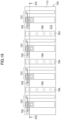
- FIG. 10 is a plan view of an example differential circuit board.
- FIG. 11 is an XI-XI cross-sectional view of the example differential circuit board shown in FIG. 10 .
- a dielectric layer 210 includes some first sections 216 .
- the dielectric layer 210 includes some second portions 218 .
- the first portions 216 and the second portions 218 are alternately arranged.
- a first conductor line 222 is disposed on a first surface 212 of each of the first portions 216 .
- a second conductor line 224 is disposed on the first surface 212 of each of the second portions 218 .
- the first conductor line 222 and the second conductor line 224 constitute differential transmission lines in each of multiple channels CH.
- Each of the first portions 216 , on the first surface 212 includes a routing area 230 in which the first conductor line 222 is formed.
- Each of the first portions 216 , on the first surface 212 includes a margin area 232 adjacent to the routing area 230 , with a margin width Wm in a direction against the second conductor line 224 .
- the first portions 216 are equal in the margin width Wm.
- a ground conductor 226 is continuous on a second surface 214 of the first portion 216 and on the second surface 214 of the second portion 218 .
- the second surface 214 has a step 220 between the first portion 216 and the second portion 218 .
- the step 220 of the second surface 214 is just below the center of the space between the first conductor line 222 and the second conductor line 224 .
- the second conductor line 224 is located at the center of the second portion 218 in the alignment direction of the first conductor line 222 and the second conductor line 224 . What is described above in relation to FIGS. 1 - 9 is applicable hereto.
- a second line-width W 2 is smaller than a first line-width W 1 in each channel CH, providing a small array-type differential circuit board.
- the distance between the adjacent channels CH may increase without changing the size of the array-type differential circuit board. This enables reduction of crosstalk.
- the distance between the adjacent channels CH may be larger, with the differential circuit board smaller.
- FIG. 12 is a cross-sectional view of an example differential circuit board.
- Each of first portions 316 on a first surface 312 , has a routing area 330 in which a first conductor line 322 is formed.
- Each of the first portions 316 on the first surface 312 , has no margin adjacent to the routing area 330 in the direction against a second conductor line 324 .
- a step 320 of a second surface 314 is just below the center of the space between the first conductor line 322 and the second conductor line 324 . What is described above in relation to FIGS. 10 - 11 is applicable hereto.
- FIG. 13 is a plan view of an example semiconductor light-emitting device.
- FIG. 14 is a XIV-XIV cross-sectional view of the example semiconductor light-emitting device shown in FIG. 13 .
- the semiconductor light-emitting device has a differential circuit board 400 . What is described above in relation to FIGS. 1 - 9 is applicable to the differential circuit board 400 .
- An optical semiconductor device 434 is mounted on the differential circuit board 400 .
- the optical semiconductor device 434 has a semiconductor laser 436 for emitting light.
- the optical semiconductor device 434 has an electro-absorption modulator 438 for modulating light by an electro-absorption effect.
- the optical semiconductor device 434 is an electro-absorption modulator integrated laser having the semiconductor laser 436 and the electro-absorption modulator 438 integrated therein.
- FIG. 15 is a cross-sectional view of an example optical semiconductor device 434 (e.g., of the example semiconductor light-emitting device described above in relation to FIGS. 13 - 14 ).
- the semiconductor laser 436 and the electro-absorption modulator 438 are built into a semiconductor substrate 440 .
- the semiconductor substrate 440 is an n-type InP substrate.
- the semiconductor laser 436 has a multi-quantum well 446 A interposed between a lower SCH (Separated Confinement Heterostructure) layer 442 A and an upper SCH layer 444 A, on the semiconductor substrate 440 .
- There is a diffraction grating layer 448 on the upper SCH layer 444 A, covered with a cladding layer 450 A.
- the laser 436 may be in a distributed bragg reflector (DBR) configuration or a distributed feedback (DFB) configuration.
- DBR distributed bragg reflector
- DFB distributed feedback
- the electro-absorption modulator 438 has a multi-quantum well 446 B interposed between a lower SCH layer 442 B and an upper SCH layer 444 B, above the semiconductor substrate 440 .
- the upper SCH layer 444 B is covered with a cladding layer 450 B.
- the cladding layer 450 A and the cladding layer 450 B may be the same material or different materials.
- the electro-absorption modulator 438 and the semiconductor laser 436 may not be integrated on the same semiconductor substrate 440 but may be formed on different semiconductor substrates 440 .
- the optical semiconductor device 434 has a lower electrode 452 (e.g., a cathode), common to the electro-absorption modulator 438 and the semiconductor laser 436 .
- the lower electrode 452 may be separately formed on each of the electro-absorption modulator 438 and the semiconductor laser 436 .
- the semiconductor laser 436 has an upper electrode 454 (e.g., anode) for applying a direct current voltage. The direct current voltage is applied between the upper electrode 454 and the lower electrode 452 .
- the optical semiconductor device 434 has an upper electrode 456 (e.g., anode) of the electro-absorption modulator 438 . An AC voltage is applied between the upper electrode 456 and the lower electrode 452 .
- the optical semiconductor device 434 (lower electrode 452 ) is opposed to a first conductor line 422 , without protrusion.
- a first line-width W 1 (e.g., as shown in FIG. 13 ) of the first conductor line 422 is set to a size enough to mount the optical semiconductor device 434 and is constant in the extending direction.
- the upper electrode 456 of the electro-absorption modulator 438 is connected to a second conductor line 424 with a wire 468 .
- the upper electrode 454 of the semiconductor laser 436 is electronically connected to the direct current source by a connection means such as a wire.
- the differential circuit board 400 has a pad 458 disposed on a first surface 412 and adjacent to the first conductor line 422 in a direction against the second conductor line 424 (e.g., as shown in FIG. 14 ).
- a pad 458 is disposed on a first portion 416 .
- the differential circuit board 400 has a matching resistor 460 connected in series between the pad 458 and the first conductor line 422 .
- the matching resistor 460 is connected for impedance matching.
- the semiconductor light-emitting device has a wire 470 configured to connect the upper electrode 456 of the electro-absorption modulator 438 and the pad 458 .
- the matching resistor 460 is connected in parallel to the electro-absorption modulator 438 .
- High-frequency signals for differential signal transmission are input to the first conductor line 422 and the second conductor line 424 .
- the high frequency signals are applied to the lower electrode 452 and the upper electrode 456 of the electro-absorption modulator 438 , respectively, for driving it by differential signals.
- FIG. 16 is a plan view of an example semiconductor light-emitting device.
- a second conductor line 524 has a stub 562 extending in a direction against a first conductor line 522 .
- the stub 562 comprises a same material or same laminated materials as the second conductor line 524 .
- the first conductor line 522 has a portion adjacent to the pad 558 and a portion, where the stub 562 extends, adjacent to the second conductor line 524 .
- the second conductor line 524 has the stub 562 , thereby being closer in electrical characteristics to the first conductor line 522 connected to the matching resistor 560 and the pad 558 .
- the high-frequency line of the first conductor line 522 and the second conductor line 524 become closer in high-frequency characteristics, improving the signal quality of a drive by differential signals. What is described above in relation to FIGS. 13 - 15 is applicable hereto.
- FIG. 17 is a plan view of an example semiconductor light-emitting device.
- FIG. 18 is an XVIII-XVIII cross-sectional view of the example light-emitting device shown in FIG. 17 .
- the example semiconductor light-emitting device has a differential circuit board 600 . What is described above in relation to FIG. 11 and FIG. 13 is applicable to the differential circuit board 600 .
- the semiconductor example light-emitting device has an optical semiconductor device 634 . What is described above in relation to FIG. 13 is applicable to the optical semiconductor device 634 .
- Each of first portions 616 , on a first surface 612 includes a routing area 630 in which a first conductor line 622 is formed.
- Each of the first portions 616 , on the first surface 612 includes a margin area 632 adjacent to the routing area 630 with a margin width Wm (e.g., as described above in relation to FIG. 11 ) in the direction against a second conductor line 624 .
- the first portions 616 are equal in the margin width Wm.
- a pad 658 is disposed on the first portion 616 .
- each channel CH high-frequency signals for differential signal transmission are input to the first conductor line 622 and the second conductor line 624 .
- the high frequency signals are applied to the lower electrode (not shown) and an upper electrode 656 of an electro-absorption modulator 638 , respectively, for the drive by differential signals.
- FIG. 19 is a plan view of an example semiconductor light-emitting device.
- FIG. 20 is a XX-XX cross-sectional view of the example semiconductor light-emitting device shown in FIG. 19 .
- a differential circuit board 700 between adjacent channels CH, has an inter-channel conductor 764 (e.g., a via, such as a filled via or a through-hole via) disposed on a first surface 712 .
- the differential circuit board 700 has a connecting conductor 766 connecting a ground conductor 726 and the inter-channel conductor 764 and penetrating a dielectric layer 710 .
- the connecting conductor 766 penetrates a first portion 716 , without penetrating a second portion 718 .
- a pad 758 is disposed on the first portion 716 .
- the inter-channel conductor 764 connected to the ground conductor 726 is disposed between the adjacent channels CH, thereby reducing the electrical crosstalk between the adjacent channels CH.
- FIG. 21 is a cross-sectional view of an example semiconductor light-emitting device.
- a differential circuit board 800 has an inter-channel conductor 864 disposed on a first surface 812 , between adjacent channels CH.
- the differential circuit board 800 penetrates a dielectric layer 810 and has a connecting conductor 866 connecting a ground conductor 826 and the inter-channel conductor 864 .
- a connecting conductor 866 penetrates a second portion 818 , without penetrating the first portion 816 .
- a pad 858 is disposed on the second portion 818 .
- the inter-channel conductor 864 is formed on the thin second portion 818 , making the through hole smaller. For example, small diameter vias can be formed. Therefore, a smaller semiconductor light-emitting device is provided.
- “at least one of: a, b, or c” is intended to cover a, b, c, a-b, a-c, b-c, and a-b-c, as well as any combination with multiple of the same item.
- the terms “has,” “have,” “having,” or the like are intended to be open-ended terms. Further, the phrase “based on” is intended to mean “based, at least in part, on” unless explicitly stated otherwise. Also, as used herein, the term “or” is intended to be inclusive when used in a series and may be used interchangeably with “and/or,” unless explicitly stated otherwise (e.g., if used in combination with “either” or “only one of”). Further, spatially relative terms, such as “below,” “lower,” “above,” “upper,” and the like, may be used herein for ease of description to describe one element or feature's relationship to another element(s) or feature(s) as illustrated in the figures.
- the spatially relative terms are intended to encompass different orientations of the apparatus, device, and/or element in use or operation in addition to the orientation depicted in the figures.
- the apparatus may be otherwise oriented (rotated 90 degrees or at other orientations) and the spatially relative descriptors used herein may likewise be interpreted accordingly.
Landscapes
- Physics & Mathematics (AREA)
- Engineering & Computer Science (AREA)
- Microelectronics & Electronic Packaging (AREA)
- Electromagnetism (AREA)
- Condensed Matter Physics & Semiconductors (AREA)
- General Physics & Mathematics (AREA)
- Optics & Photonics (AREA)
- Semiconductor Lasers (AREA)
Abstract
Description
Claims (20)
Priority Applications (2)
| Application Number | Priority Date | Filing Date | Title |
|---|---|---|---|
| TW110131284A TW202226688A (en) | 2020-09-14 | 2021-08-24 | Differential circuit board and semiconductor light-emitting device |
| CN202111067632.6A CN114189977A (en) | 2020-09-14 | 2021-09-13 | Differential circuit board and semiconductor light emitting device |
Applications Claiming Priority (4)
| Application Number | Priority Date | Filing Date | Title |
|---|---|---|---|
| JP2020153685 | 2020-09-14 | ||
| JP2020-153685 | 2020-09-14 | ||
| JP2020186989A JP7621092B2 (en) | 2020-09-14 | 2020-11-10 | Differential wiring board and semiconductor light emitting device |
| JP2020-186989 | 2020-11-10 |
Publications (2)
| Publication Number | Publication Date |
|---|---|
| US20220087007A1 US20220087007A1 (en) | 2022-03-17 |
| US12082336B2 true US12082336B2 (en) | 2024-09-03 |
Family
ID=80628038
Family Applications (1)
| Application Number | Title | Priority Date | Filing Date |
|---|---|---|---|
| US17/216,118 Active 2043-03-28 US12082336B2 (en) | 2020-09-14 | 2021-03-29 | Differential circuit board and semiconductor light emitting device |
Country Status (1)
| Country | Link |
|---|---|
| US (1) | US12082336B2 (en) |
Citations (24)
| Publication number | Priority date | Publication date | Assignee | Title |
|---|---|---|---|---|
| JPH01257355A (en) | 1987-12-14 | 1989-10-13 | Mitsubishi Electric Corp | Microwave monolithic ic |
| US5652557A (en) * | 1994-10-19 | 1997-07-29 | Mitsubishi Denki Kabushiki Kaisha | Transmission lines and fabricating method thereof |
| JPH09223851A (en) | 1996-02-14 | 1997-08-26 | Oki Electric Ind Co Ltd | Semiconductor integrated circuit board and method for forming it |
| JP2002100842A (en) | 2000-09-22 | 2002-04-05 | Sumitomo Wiring Syst Ltd | Flexible flat wiring board and method of adjusting its impedance |
| JP2003043437A (en) | 2001-08-01 | 2003-02-13 | Sumitomo Osaka Cement Co Ltd | Light modulator |
| JP2004140134A (en) | 2002-10-17 | 2004-05-13 | Toshiba Corp | Hybrid semiconductor device |
| US20060028305A1 (en) * | 2004-08-03 | 2006-02-09 | Banpil Photonics, Inc. | High-Speed Printed Circuit Boards (PCBs) and Manufacturing |
| US20070194434A1 (en) * | 2006-02-20 | 2007-08-23 | Chin-Sung Lin | Differential signal transmission structure, wiring board, and chip package |
| US20080023804A1 (en) * | 2004-11-24 | 2008-01-31 | Banpil Photonics, Inc. | High-speed electrical interconnects and method of manufacturing |
| US20080073747A1 (en) | 2006-09-22 | 2008-03-27 | Clinton Chao | Electromagnetic shielding using through-silicon vias |
| US20110019371A1 (en) * | 2009-07-24 | 2011-01-27 | Hon Hai Precision Industry Co., Ltd. | Flexible printed circuit board |
| CN102378488A (en) | 2010-08-23 | 2012-03-14 | 大唐移动通信设备有限公司 | Printed circuit board and design method thereof |
| US20140010495A1 (en) | 2012-07-09 | 2014-01-09 | Bae Systems Information And Electronic Systems Integration Inc. | Method for fabricating silicon photonic waveguides |
| US20150173256A1 (en) * | 2013-12-17 | 2015-06-18 | Lenovo Enterprise Solutions (Singapore) Pte. Ltd. | Emi suppression technique using a transmission line grating |
| US20160174361A1 (en) * | 2014-12-11 | 2016-06-16 | Intel Corporation | Signal routing |
| US20160174374A1 (en) * | 2014-12-12 | 2016-06-16 | Intel Corporation | Vertical trench routing in a substrate |
| WO2016152152A1 (en) | 2015-03-23 | 2016-09-29 | 日本電信電話株式会社 | High-frequency transmission line and optical circuit |
| US20170156203A1 (en) * | 2015-11-27 | 2017-06-01 | Chung Yuan Christian University | Circuit board |
| US20190044301A1 (en) | 2017-08-02 | 2019-02-07 | Oclaro Japan, Inc. | Semiconductor light-emitting device |
| JP2019029649A (en) | 2017-08-02 | 2019-02-21 | 日本オクラロ株式会社 | Semiconductor light emitting device |
| US20190069391A1 (en) * | 2018-10-25 | 2019-02-28 | Intel Corporation | High-density dual-embedded microstrip interconnects |
| US10849220B1 (en) * | 2020-01-23 | 2020-11-24 | Super Micro Computer, Inc. | Setting the impedance of signal traces of a circuit board using a reference trace |
| US20200395318A1 (en) * | 2019-06-12 | 2020-12-17 | Intel Corporation | 3d trench reference planes for integrated-circuit die packages |
| US10903543B2 (en) * | 2016-12-06 | 2021-01-26 | Hewlett Packard Enterprise Development Lp | PCB transmission lines having reduced loss |
-
2021
- 2021-03-29 US US17/216,118 patent/US12082336B2/en active Active
Patent Citations (27)
| Publication number | Priority date | Publication date | Assignee | Title |
|---|---|---|---|---|
| JPH01257355A (en) | 1987-12-14 | 1989-10-13 | Mitsubishi Electric Corp | Microwave monolithic ic |
| US4956697A (en) | 1987-12-14 | 1990-09-11 | Mitsubishi Denki Kabushiki Kaisha | Microwave monolithic integrated circuit with heat radiating electrode |
| US5652557A (en) * | 1994-10-19 | 1997-07-29 | Mitsubishi Denki Kabushiki Kaisha | Transmission lines and fabricating method thereof |
| JPH09223851A (en) | 1996-02-14 | 1997-08-26 | Oki Electric Ind Co Ltd | Semiconductor integrated circuit board and method for forming it |
| JP2002100842A (en) | 2000-09-22 | 2002-04-05 | Sumitomo Wiring Syst Ltd | Flexible flat wiring board and method of adjusting its impedance |
| JP2003043437A (en) | 2001-08-01 | 2003-02-13 | Sumitomo Osaka Cement Co Ltd | Light modulator |
| US7397974B2 (en) | 2001-08-01 | 2008-07-08 | Sumitomo Osaka Cement Co., Ltd. | Optical modulator |
| JP2004140134A (en) | 2002-10-17 | 2004-05-13 | Toshiba Corp | Hybrid semiconductor device |
| US20060028305A1 (en) * | 2004-08-03 | 2006-02-09 | Banpil Photonics, Inc. | High-Speed Printed Circuit Boards (PCBs) and Manufacturing |
| US20080023804A1 (en) * | 2004-11-24 | 2008-01-31 | Banpil Photonics, Inc. | High-speed electrical interconnects and method of manufacturing |
| US20070194434A1 (en) * | 2006-02-20 | 2007-08-23 | Chin-Sung Lin | Differential signal transmission structure, wiring board, and chip package |
| US20080073747A1 (en) | 2006-09-22 | 2008-03-27 | Clinton Chao | Electromagnetic shielding using through-silicon vias |
| US20110019371A1 (en) * | 2009-07-24 | 2011-01-27 | Hon Hai Precision Industry Co., Ltd. | Flexible printed circuit board |
| CN102378488A (en) | 2010-08-23 | 2012-03-14 | 大唐移动通信设备有限公司 | Printed circuit board and design method thereof |
| US20140010495A1 (en) | 2012-07-09 | 2014-01-09 | Bae Systems Information And Electronic Systems Integration Inc. | Method for fabricating silicon photonic waveguides |
| US20150173256A1 (en) * | 2013-12-17 | 2015-06-18 | Lenovo Enterprise Solutions (Singapore) Pte. Ltd. | Emi suppression technique using a transmission line grating |
| US20160174361A1 (en) * | 2014-12-11 | 2016-06-16 | Intel Corporation | Signal routing |
| US20160174374A1 (en) * | 2014-12-12 | 2016-06-16 | Intel Corporation | Vertical trench routing in a substrate |
| US10866439B2 (en) | 2015-03-23 | 2020-12-15 | Nippon Telegraph And Telephone Corporation | High-frequency transmission line and optical circuit |
| WO2016152152A1 (en) | 2015-03-23 | 2016-09-29 | 日本電信電話株式会社 | High-frequency transmission line and optical circuit |
| US20170156203A1 (en) * | 2015-11-27 | 2017-06-01 | Chung Yuan Christian University | Circuit board |
| US10903543B2 (en) * | 2016-12-06 | 2021-01-26 | Hewlett Packard Enterprise Development Lp | PCB transmission lines having reduced loss |
| JP2019029649A (en) | 2017-08-02 | 2019-02-21 | 日本オクラロ株式会社 | Semiconductor light emitting device |
| US20190044301A1 (en) | 2017-08-02 | 2019-02-07 | Oclaro Japan, Inc. | Semiconductor light-emitting device |
| US20190069391A1 (en) * | 2018-10-25 | 2019-02-28 | Intel Corporation | High-density dual-embedded microstrip interconnects |
| US20200395318A1 (en) * | 2019-06-12 | 2020-12-17 | Intel Corporation | 3d trench reference planes for integrated-circuit die packages |
| US10849220B1 (en) * | 2020-01-23 | 2020-11-24 | Super Micro Computer, Inc. | Setting the impedance of signal traces of a circuit board using a reference trace |
Non-Patent Citations (1)
| Title |
|---|
| H.R. Kaupp, "Characteristics of Microstrip Transmission Lines", IEEE Transactions on Electronic Computers, Apr. 1967, 9 pages, vol. EC-16, Issue No. 2. |
Also Published As
| Publication number | Publication date |
|---|---|
| US20220087007A1 (en) | 2022-03-17 |
Similar Documents
| Publication | Publication Date | Title |
|---|---|---|
| US6573600B2 (en) | Multilayer wiring substrate having differential signal wires and a general signal wire in different planes | |
| CA2351975C (en) | Vertical transition device for differential stripline paths and optical module | |
| US6807065B2 (en) | Multilayer printed circuit board | |
| CN107430293B (en) | Optical circuit | |
| US11206087B2 (en) | Optical module and optical transmitter | |
| US10299368B2 (en) | Surface integrated waveguides and circuit structures therefor | |
| SE522404C2 (en) | directional Couplers | |
| CN107072032B (en) | A flexible printed circuit board structure | |
| US20190182949A1 (en) | Flexible printed circuit board and optical module | |
| US20010040490A1 (en) | Transmission line and transmission line resonator | |
| US20060261465A1 (en) | Circuit board with trace configuration for high-speed digital differential signaling | |
| CN114189977A (en) | Differential circuit board and semiconductor light emitting device | |
| CN100568614C (en) | Triangular conformal transport structure | |
| JPH10200311A (en) | Coplanar waveguide line with back ground conductor | |
| US12082336B2 (en) | Differential circuit board and semiconductor light emitting device | |
| JP5207065B2 (en) | High frequency transmission line | |
| JP7126314B2 (en) | semiconductor light emitting device | |
| JPWO2018198197A1 (en) | Light modulator | |
| WO2023188450A1 (en) | Antenna substrate | |
| JP7621092B2 (en) | Differential wiring board and semiconductor light emitting device | |
| JP2006351647A (en) | Wiring board | |
| US10541510B2 (en) | Semiconductor light-emitting device | |
| JP2011130395A (en) | Signal combination and distribution circuit, power amplifier and method of manufacturing signal combination and distribution circuit | |
| US6433650B1 (en) | Electrical transmission arrangement | |
| US7064625B2 (en) | Transmission line structures |
Legal Events
| Date | Code | Title | Description |
|---|---|---|---|
| AS | Assignment |
Owner name: LUMENTUM JAPAN, INC., JAPAN Free format text: ASSIGNMENT OF ASSIGNORS INTEREST;ASSIGNOR:ADACHI, KOICHIRO;REEL/FRAME:055757/0938 Effective date: 20210127 |
|
| FEPP | Fee payment procedure |
Free format text: ENTITY STATUS SET TO UNDISCOUNTED (ORIGINAL EVENT CODE: BIG.); ENTITY STATUS OF PATENT OWNER: LARGE ENTITY |
|
| STPP | Information on status: patent application and granting procedure in general |
Free format text: DOCKETED NEW CASE - READY FOR EXAMINATION |
|
| STPP | Information on status: patent application and granting procedure in general |
Free format text: NOTICE OF ALLOWANCE MAILED -- APPLICATION RECEIVED IN OFFICE OF PUBLICATIONS |
|
| ZAAA | Notice of allowance and fees due |
Free format text: ORIGINAL CODE: NOA |
|
| ZAAB | Notice of allowance mailed |
Free format text: ORIGINAL CODE: MN/=. |
|
| STPP | Information on status: patent application and granting procedure in general |
Free format text: NOTICE OF ALLOWANCE MAILED -- APPLICATION RECEIVED IN OFFICE OF PUBLICATIONS |
|
| STPP | Information on status: patent application and granting procedure in general |
Free format text: NOTICE OF ALLOWANCE MAILED -- APPLICATION RECEIVED IN OFFICE OF PUBLICATIONS |
|
| ZAAA | Notice of allowance and fees due |
Free format text: ORIGINAL CODE: NOA |
|
| STPP | Information on status: patent application and granting procedure in general |
Free format text: PUBLICATIONS -- ISSUE FEE PAYMENT VERIFIED |
|
| STPP | Information on status: patent application and granting procedure in general |
Free format text: NOTICE OF ALLOWANCE MAILED -- APPLICATION RECEIVED IN OFFICE OF PUBLICATIONS |
|
| STPP | Information on status: patent application and granting procedure in general |
Free format text: PUBLICATIONS -- ISSUE FEE PAYMENT VERIFIED |
|
| STCF | Information on status: patent grant |
Free format text: PATENTED CASE |
|
| CC | Certificate of correction |