US12074152B2 - Display device - Google Patents
Display device Download PDFInfo
- Publication number
- US12074152B2 US12074152B2 US17/410,053 US202117410053A US12074152B2 US 12074152 B2 US12074152 B2 US 12074152B2 US 202117410053 A US202117410053 A US 202117410053A US 12074152 B2 US12074152 B2 US 12074152B2
- Authority
- US
- United States
- Prior art keywords
- test electrode
- test
- amd
- facing
- film
- Prior art date
- Legal status (The legal status is an assumption and is not a legal conclusion. Google has not performed a legal analysis and makes no representation as to the accuracy of the status listed.)
- Active, expires
Links
Images


Classifications
-
- H10W90/00—
-
- H—ELECTRICITY
- H01—ELECTRIC ELEMENTS
- H01L—SEMICONDUCTOR DEVICES NOT COVERED BY CLASS H10
- H01L25/00—Assemblies consisting of a plurality of semiconductor or other solid state devices
- H01L25/18—Assemblies consisting of a plurality of semiconductor or other solid state devices the devices being of the types provided for in two or more different main groups of the same subclass of H10B, H10D, H10F, H10H, H10K or H10N
-
- H—ELECTRICITY
- H10—SEMICONDUCTOR DEVICES; ELECTRIC SOLID-STATE DEVICES NOT OTHERWISE PROVIDED FOR
- H10K—ORGANIC ELECTRIC SOLID-STATE DEVICES
- H10K59/00—Integrated devices, or assemblies of multiple devices, comprising at least one organic light-emitting element covered by group H10K50/00
- H10K59/10—OLED displays
- H10K59/12—Active-matrix OLED [AMOLED] displays
- H10K59/131—Interconnections, e.g. wiring lines or terminals
-
- G—PHYSICS
- G09—EDUCATION; CRYPTOGRAPHY; DISPLAY; ADVERTISING; SEALS
- G09G—ARRANGEMENTS OR CIRCUITS FOR CONTROL OF INDICATING DEVICES USING STATIC MEANS TO PRESENT VARIABLE INFORMATION
- G09G3/00—Control arrangements or circuits, of interest only in connection with visual indicators other than cathode-ray tubes
- G09G3/006—Electronic inspection or testing of displays and display drivers, e.g. of LED or LCD displays
-
- H—ELECTRICITY
- H01—ELECTRIC ELEMENTS
- H01L—SEMICONDUCTOR DEVICES NOT COVERED BY CLASS H10
- H01L22/00—Testing or measuring during manufacture or treatment; Reliability measurements, i.e. testing of parts without further processing to modify the parts as such; Structural arrangements therefor
- H01L22/30—Structural arrangements specially adapted for testing or measuring during manufacture or treatment, or specially adapted for reliability measurements
- H01L22/32—Additional lead-in metallisation on a device or substrate, e.g. additional pads or pad portions, lines in the scribe line, sacrificed conductors
-
- H—ELECTRICITY
- H01—ELECTRIC ELEMENTS
- H01L—SEMICONDUCTOR DEVICES NOT COVERED BY CLASS H10
- H01L23/00—Details of semiconductor or other solid state devices
- H01L23/48—Arrangements for conducting electric current to or from the solid state body in operation, e.g. leads, terminal arrangements ; Selection of materials therefor
- H01L23/488—Arrangements for conducting electric current to or from the solid state body in operation, e.g. leads, terminal arrangements ; Selection of materials therefor consisting of soldered or bonded constructions
- H01L23/498—Leads, i.e. metallisations or lead-frames on insulating substrates, e.g. chip carriers
- H01L23/49838—Geometry or layout
-
- H—ELECTRICITY
- H01—ELECTRIC ELEMENTS
- H01L—SEMICONDUCTOR DEVICES NOT COVERED BY CLASS H10
- H01L24/00—Arrangements for connecting or disconnecting semiconductor or solid-state bodies; Methods or apparatus related thereto
- H01L24/01—Means for bonding being attached to, or being formed on, the surface to be connected, e.g. chip-to-package, die-attach, "first-level" interconnects; Manufacturing methods related thereto
- H01L24/02—Bonding areas ; Manufacturing methods related thereto
- H01L24/04—Structure, shape, material or disposition of the bonding areas prior to the connecting process
- H01L24/06—Structure, shape, material or disposition of the bonding areas prior to the connecting process of a plurality of bonding areas
-
- H—ELECTRICITY
- H01—ELECTRIC ELEMENTS
- H01L—SEMICONDUCTOR DEVICES NOT COVERED BY CLASS H10
- H01L24/00—Arrangements for connecting or disconnecting semiconductor or solid-state bodies; Methods or apparatus related thereto
- H01L24/01—Means for bonding being attached to, or being formed on, the surface to be connected, e.g. chip-to-package, die-attach, "first-level" interconnects; Manufacturing methods related thereto
- H01L24/26—Layer connectors, e.g. plate connectors, solder or adhesive layers; Manufacturing methods related thereto
- H01L24/31—Structure, shape, material or disposition of the layer connectors after the connecting process
- H01L24/32—Structure, shape, material or disposition of the layer connectors after the connecting process of an individual layer connector
-
- H—ELECTRICITY
- H01—ELECTRIC ELEMENTS
- H01L—SEMICONDUCTOR DEVICES NOT COVERED BY CLASS H10
- H01L24/00—Arrangements for connecting or disconnecting semiconductor or solid-state bodies; Methods or apparatus related thereto
- H01L24/80—Methods for connecting semiconductor or other solid state bodies using means for bonding being attached to, or being formed on, the surface to be connected
- H01L24/83—Methods for connecting semiconductor or other solid state bodies using means for bonding being attached to, or being formed on, the surface to be connected using a layer connector
-
- H—ELECTRICITY
- H05—ELECTRIC TECHNIQUES NOT OTHERWISE PROVIDED FOR
- H05K—PRINTED CIRCUITS; CASINGS OR CONSTRUCTIONAL DETAILS OF ELECTRIC APPARATUS; MANUFACTURE OF ASSEMBLAGES OF ELECTRICAL COMPONENTS
- H05K1/00—Printed circuits
- H05K1/02—Details
- H05K1/0266—Marks, test patterns or identification means
- H05K1/0268—Marks, test patterns or identification means for electrical inspection or testing
-
- H—ELECTRICITY
- H05—ELECTRIC TECHNIQUES NOT OTHERWISE PROVIDED FOR
- H05K—PRINTED CIRCUITS; CASINGS OR CONSTRUCTIONAL DETAILS OF ELECTRIC APPARATUS; MANUFACTURE OF ASSEMBLAGES OF ELECTRICAL COMPONENTS
- H05K1/00—Printed circuits
- H05K1/02—Details
- H05K1/11—Printed elements for providing electric connections to or between printed circuits
- H05K1/111—Pads for surface mounting, e.g. lay-out
-
- H—ELECTRICITY
- H05—ELECTRIC TECHNIQUES NOT OTHERWISE PROVIDED FOR
- H05K—PRINTED CIRCUITS; CASINGS OR CONSTRUCTIONAL DETAILS OF ELECTRIC APPARATUS; MANUFACTURE OF ASSEMBLAGES OF ELECTRICAL COMPONENTS
- H05K3/00—Apparatus or processes for manufacturing printed circuits
- H05K3/30—Assembling printed circuits with electric components, e.g. with resistor
- H05K3/32—Assembling printed circuits with electric components, e.g. with resistor electrically connecting electric components or wires to printed circuits
- H05K3/321—Assembling printed circuits with electric components, e.g. with resistor electrically connecting electric components or wires to printed circuits by conductive adhesives
-
- H10P72/50—
-
- H10P74/273—
-
- H10W46/00—
-
- H10W70/65—
-
- H—ELECTRICITY
- H01—ELECTRIC ELEMENTS
- H01L—SEMICONDUCTOR DEVICES NOT COVERED BY CLASS H10
- H01L2224/00—Indexing scheme for arrangements for connecting or disconnecting semiconductor or solid-state bodies and methods related thereto as covered by H01L24/00
- H01L2224/01—Means for bonding being attached to, or being formed on, the surface to be connected, e.g. chip-to-package, die-attach, "first-level" interconnects; Manufacturing methods related thereto
- H01L2224/02—Bonding areas; Manufacturing methods related thereto
- H01L2224/04—Structure, shape, material or disposition of the bonding areas prior to the connecting process
- H01L2224/06—Structure, shape, material or disposition of the bonding areas prior to the connecting process of a plurality of bonding areas
- H01L2224/061—Disposition
- H01L2224/0612—Layout
- H01L2224/0616—Random array, i.e. array with no symmetry
- H01L2224/06164—Random array, i.e. array with no symmetry covering only portions of the surface to be connected
- H01L2224/06165—Covering only the peripheral area of the surface to be connected, i.e. peripheral arrangements
-
- H—ELECTRICITY
- H01—ELECTRIC ELEMENTS
- H01L—SEMICONDUCTOR DEVICES NOT COVERED BY CLASS H10
- H01L2224/00—Indexing scheme for arrangements for connecting or disconnecting semiconductor or solid-state bodies and methods related thereto as covered by H01L24/00
- H01L2224/01—Means for bonding being attached to, or being formed on, the surface to be connected, e.g. chip-to-package, die-attach, "first-level" interconnects; Manufacturing methods related thereto
- H01L2224/26—Layer connectors, e.g. plate connectors, solder or adhesive layers; Manufacturing methods related thereto
- H01L2224/31—Structure, shape, material or disposition of the layer connectors after the connecting process
- H01L2224/32—Structure, shape, material or disposition of the layer connectors after the connecting process of an individual layer connector
- H01L2224/321—Disposition
- H01L2224/32151—Disposition the layer connector connecting between a semiconductor or solid-state body and an item not being a semiconductor or solid-state body, e.g. chip-to-substrate, chip-to-passive
- H01L2224/32221—Disposition the layer connector connecting between a semiconductor or solid-state body and an item not being a semiconductor or solid-state body, e.g. chip-to-substrate, chip-to-passive the body and the item being stacked
- H01L2224/32225—Disposition the layer connector connecting between a semiconductor or solid-state body and an item not being a semiconductor or solid-state body, e.g. chip-to-substrate, chip-to-passive the body and the item being stacked the item being non-metallic, e.g. insulating substrate with or without metallisation
- H01L2224/32227—Disposition the layer connector connecting between a semiconductor or solid-state body and an item not being a semiconductor or solid-state body, e.g. chip-to-substrate, chip-to-passive the body and the item being stacked the item being non-metallic, e.g. insulating substrate with or without metallisation the layer connector connecting to a bond pad of the item
-
- H—ELECTRICITY
- H01—ELECTRIC ELEMENTS
- H01L—SEMICONDUCTOR DEVICES NOT COVERED BY CLASS H10
- H01L2224/00—Indexing scheme for arrangements for connecting or disconnecting semiconductor or solid-state bodies and methods related thereto as covered by H01L24/00
- H01L2224/80—Methods for connecting semiconductor or other solid state bodies using means for bonding being attached to, or being formed on, the surface to be connected
- H01L2224/83—Methods for connecting semiconductor or other solid state bodies using means for bonding being attached to, or being formed on, the surface to be connected using a layer connector
- H01L2224/8312—Aligning
- H01L2224/83121—Active alignment, i.e. by apparatus steering, e.g. optical alignment using marks or sensors
- H01L2224/8313—Active alignment, i.e. by apparatus steering, e.g. optical alignment using marks or sensors using marks formed on the semiconductor or solid-state body
-
- H—ELECTRICITY
- H01—ELECTRIC ELEMENTS
- H01L—SEMICONDUCTOR DEVICES NOT COVERED BY CLASS H10
- H01L2224/00—Indexing scheme for arrangements for connecting or disconnecting semiconductor or solid-state bodies and methods related thereto as covered by H01L24/00
- H01L2224/80—Methods for connecting semiconductor or other solid state bodies using means for bonding being attached to, or being formed on, the surface to be connected
- H01L2224/83—Methods for connecting semiconductor or other solid state bodies using means for bonding being attached to, or being formed on, the surface to be connected using a layer connector
- H01L2224/8312—Aligning
- H01L2224/83121—Active alignment, i.e. by apparatus steering, e.g. optical alignment using marks or sensors
- H01L2224/83132—Active alignment, i.e. by apparatus steering, e.g. optical alignment using marks or sensors using marks formed outside the semiconductor or solid-state body, i.e. "off-chip"
-
- H—ELECTRICITY
- H01—ELECTRIC ELEMENTS
- H01L—SEMICONDUCTOR DEVICES NOT COVERED BY CLASS H10
- H01L2224/00—Indexing scheme for arrangements for connecting or disconnecting semiconductor or solid-state bodies and methods related thereto as covered by H01L24/00
- H01L2224/80—Methods for connecting semiconductor or other solid state bodies using means for bonding being attached to, or being formed on, the surface to be connected
- H01L2224/83—Methods for connecting semiconductor or other solid state bodies using means for bonding being attached to, or being formed on, the surface to be connected using a layer connector
- H01L2224/838—Bonding techniques
- H01L2224/8385—Bonding techniques using a polymer adhesive, e.g. an adhesive based on silicone, epoxy, polyimide, polyester
- H01L2224/83851—Bonding techniques using a polymer adhesive, e.g. an adhesive based on silicone, epoxy, polyimide, polyester being an anisotropic conductive adhesive
-
- H—ELECTRICITY
- H01—ELECTRIC ELEMENTS
- H01L—SEMICONDUCTOR DEVICES NOT COVERED BY CLASS H10
- H01L2224/00—Indexing scheme for arrangements for connecting or disconnecting semiconductor or solid-state bodies and methods related thereto as covered by H01L24/00
- H01L2224/80—Methods for connecting semiconductor or other solid state bodies using means for bonding being attached to, or being formed on, the surface to be connected
- H01L2224/83—Methods for connecting semiconductor or other solid state bodies using means for bonding being attached to, or being formed on, the surface to be connected using a layer connector
- H01L2224/83908—Methods for connecting semiconductor or other solid state bodies using means for bonding being attached to, or being formed on, the surface to be connected using a layer connector involving monitoring, e.g. feedback loop
-
- H—ELECTRICITY
- H05—ELECTRIC TECHNIQUES NOT OTHERWISE PROVIDED FOR
- H05K—PRINTED CIRCUITS; CASINGS OR CONSTRUCTIONAL DETAILS OF ELECTRIC APPARATUS; MANUFACTURE OF ASSEMBLAGES OF ELECTRICAL COMPONENTS
- H05K1/00—Printed circuits
- H05K1/02—Details
- H05K1/14—Structural association of two or more printed circuits
- H05K1/147—Structural association of two or more printed circuits at least one of the printed circuits being bent or folded, e.g. by using a flexible printed circuit
-
- H—ELECTRICITY
- H05—ELECTRIC TECHNIQUES NOT OTHERWISE PROVIDED FOR
- H05K—PRINTED CIRCUITS; CASINGS OR CONSTRUCTIONAL DETAILS OF ELECTRIC APPARATUS; MANUFACTURE OF ASSEMBLAGES OF ELECTRICAL COMPONENTS
- H05K1/00—Printed circuits
- H05K1/18—Printed circuits structurally associated with non-printed electric components
- H05K1/189—Printed circuits structurally associated with non-printed electric components characterised by the use of a flexible or folded printed circuit
-
- H—ELECTRICITY
- H05—ELECTRIC TECHNIQUES NOT OTHERWISE PROVIDED FOR
- H05K—PRINTED CIRCUITS; CASINGS OR CONSTRUCTIONAL DETAILS OF ELECTRIC APPARATUS; MANUFACTURE OF ASSEMBLAGES OF ELECTRICAL COMPONENTS
- H05K2201/00—Indexing scheme relating to printed circuits covered by H05K1/00
- H05K2201/10—Details of components or other objects attached to or integrated in a printed circuit board
- H05K2201/10007—Types of components
- H05K2201/10128—Display
-
- H—ELECTRICITY
- H05—ELECTRIC TECHNIQUES NOT OTHERWISE PROVIDED FOR
- H05K—PRINTED CIRCUITS; CASINGS OR CONSTRUCTIONAL DETAILS OF ELECTRIC APPARATUS; MANUFACTURE OF ASSEMBLAGES OF ELECTRICAL COMPONENTS
- H05K2201/00—Indexing scheme relating to printed circuits covered by H05K1/00
- H05K2201/10—Details of components or other objects attached to or integrated in a printed circuit board
- H05K2201/10227—Other objects, e.g. metallic pieces
- H05K2201/10378—Interposers
-
- H—ELECTRICITY
- H05—ELECTRIC TECHNIQUES NOT OTHERWISE PROVIDED FOR
- H05K—PRINTED CIRCUITS; CASINGS OR CONSTRUCTIONAL DETAILS OF ELECTRIC APPARATUS; MANUFACTURE OF ASSEMBLAGES OF ELECTRICAL COMPONENTS
- H05K3/00—Apparatus or processes for manufacturing printed circuits
- H05K3/30—Assembling printed circuits with electric components, e.g. with resistor
- H05K3/32—Assembling printed circuits with electric components, e.g. with resistor electrically connecting electric components or wires to printed circuits
- H05K3/321—Assembling printed circuits with electric components, e.g. with resistor electrically connecting electric components or wires to printed circuits by conductive adhesives
- H05K3/323—Assembling printed circuits with electric components, e.g. with resistor electrically connecting electric components or wires to printed circuits by conductive adhesives by applying an anisotropic conductive adhesive layer over an array of pads
-
- H10W46/301—
-
- H10W70/688—
-
- H10W72/07323—
-
- H10W72/07331—
-
- H10W72/074—
-
- H10W72/9445—
-
- H10W90/734—
Definitions
- the disclosure relates to a display device, and a method of fabricating the display device.
- Electronic devices that provide images to a user may include a display device for displaying images.
- a smart phone such as a smart phone, a tablet personal computer (“PC”), a digital camera, a laptop computer, a navigation device and a smart television (“TV”)
- PC personal computer
- TV smart television
- a display device includes a plurality of pads and alignment marks.
- a flexible film e.g., a chip-on-film (“COF”) having a driving circuit and the like mounted thereon is typically coupled to the plurality of pads, to transmit driving signals to pixels.
- the alignment marks may be used to align the substrate of the display device with the flexible film.
- the flexible film may include a plurality of leads coupled to the plurality of pads.
- the leads may be bonded to the pads separated from one another.
- Embodiments of the disclosure provide a display device that can measure an insulation resistance and an insulation gap, and a method for manufacturing a display device.
- An embodiment of a display device includes a display panel, a first film attached to the display panel, an adhesive member interposed between the display panel and the first film and extending in a first direction to attach the display panel to the first film, a first test electrode covered by the adhesive member: a second test electrode covered by the adhesive member and spaced apart from the first test electrode in a second direction perpendicular to the first direction, and test lines comprising a first test line electrically connected to the first test electrode and a second test line electrically connected to the second test electrode, where the adhesive member is disposed between the first test electrode and the second test electrode in the second direction.
- An embodiment of a display device includes a display panel, a first film attached to the display panel, a first alignment mark disposed on one of the display panel and the first film, and a second alignment mark disposed on the other of the display panel and the first film and facing the first alignment mark, where the first alignment mark comprises a first test electrode, a second test electrode and a third test electrode, which are separated from one another, where the first test electrode of the first alignment mark includes a first facing area facing the second test electrode, the second test electrode includes a second facing area facing the first test electrode and a third facing area facing the third test electrode, and the third test electrode includes a fourth facing area facing the second test electrode, and where the first facing area, the second facing area, the third facing area and the fourth facing area have a same width as one another.
- An embodiment of a method of fabricating a display device includes aligning a display panel with a first film by using a first alignment mark disposed on the display panel and a second alignment mark disposed on the first film, attaching the display panel to the first film by an adhesive member, and measuring an insulation resistance of the adhesive member through at least one of the first alignment mark and the second alignment mark, where the at least one of the first alignment mark and the second alignment mark includes a first test electrode and a second test electrode, which are separated from and insulated from each other, and where the measuring the insulation resistance of the adhesive member includes measuring the insulation resistance of the adhesive member disposed between the first test electrode and the second test electrode.
- an insulation resistance may be measured and an insulation gap may be determined.
- FIG. 1 is a plan view showing the layout of a display device according to an embodiment of the disclosure:
- FIG. 2 is a cross-sectional view showing a stack structure of a display device according to an embodiment of the disclosure:
- FIG. 3 is a schematic plan view showing a layout of a display panel, a first film and a second film of a display device according to an embodiment:
- FIG. 4 is a view showing the display panel, the first film and the second film of FIG. 3 , which are separated from one another:
- FIG. 5 is an enlarged plan view showing the first alignment mark and the second alignment mark overlapping in the display device according to an embodiment:
- FIG. 6 is a plan view showing the first alignment mark and the second alignment mark separated from each other in the display device according to an embodiment:
- FIG. 7 is a cross-sectional view taken along line VII-VII′ of FIG. 5 ;
- FIG. 8 is a view for illustrating a method of fabricating a display device according to an embodiment of the disclosure.
- FIG. 9 is a circuit diagram illustrating a method of measuring insulation resistance:
- FIG. 10 is a plan view of a first alignment mark according to an alternative embodiment:
- FIG. 11 is a plan view of a first alignment mark according to another alternative embodiment:
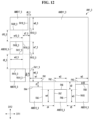
- FIG. 12 is a plan view of a first alignment mark according to yet another alternative embodiment:
- FIG. 13 is a view showing a display panel, a first film and a second film of a display device, which are separated from one another, according to an alternative embodiment:
- FIG. 14 is a plan view of a display device according to an alternative embodiment of the disclosure:
- FIG. 15 is a view showing a display panel and a second film of a display device, which are coupled with each other, according to an alternative embodiment:
- FIG. 16 is a view showing the display panel and the second film of FIG. 15 , which are separated from each other:
- FIG. 17 is a view showing a display panel and a second film of a display device, which are coupled with each other, according to another alternative embodiment:
- FIG. 18 is a view showing the display panel and the second film of FIG. 17 , which are separated from each other;
- FIG. 19 is a schematic plan view showing a layout of a display panel, a first film and a second film of a display device according to yet another alternative embodiment.
- FIG. 20 is a view showing the display panel, the first film and the second film of FIG. 19 , which are separated from one another.
- first”, “second”, etc. may be used herein to describe various elements, these elements, should not be limited by these terms. These terms may be used to distinguish one element from another element. Thus, a first element discussed below may be termed a second element without departing from teachings of one or more embodiments. The description of an element as a “first” element may not require or imply the presence of a second element or other elements.
- the terms “first”, “second”, etc. may also be used herein to differentiate different categories or sets of elements. For conciseness, the terms “first”, “second”, etc. may represent “first-category (or first-set)”, “second-category (or second-set)”, etc., respectively.
- relative terms such as “lower” or “bottom” and “upper” or “top,” may be used herein to describe one element's relationship to another element as illustrated in the Figures. It will be understood that relative terms are intended to encompass different orientations of the device in addition to the orientation depicted in the Figures. For example, if the device in one of the figures is turned over, elements described as being on the “lower” side of other elements would then be oriented on “upper” sides of the other elements. The term “lower,” can therefore, encompasses both an orientation of “lower” and “upper,” depending on the particular orientation of the figure.
- “About” or “approximately” as used herein is inclusive of the stated value and means within an acceptable range of deviation for the particular value as determined by one of ordinary skill in the art, considering the measurement in question and the error associated with measurement of the particular quantity (i.e., the limitations of the measurement system). For example, “about” can mean within one or more standard deviations, or within +30%, +20%, +10% or +5% of the stated value.
- Embodiments are described herein with reference to cross section illustrations that are schematic illustrations of idealized embodiments. As such, variations from the shapes of the illustrations as a result, for example, of manufacturing techniques and/or tolerances, are to be expected. Thus, embodiments described herein should not be construed as limited to the particular shapes of regions as illustrated herein but are to include deviations in shapes that result, for example, from manufacturing. For example, a region illustrated or described as flat may, typically, have rough and/or nonlinear features. Moreover, sharp angles that are illustrated may be rounded. Thus, the regions illustrated in the figures are schematic in nature and their shapes are not intended to illustrate the precise shape of a region and are not intended to limit the scope of the present claims.
- FIG. 1 is a plan view showing the layout of a display device according to an embodiment of the disclosure.
- a display device 1 displays moving images or still images.
- the display device 1 may be used as the display screen of portable electronic devices such as a mobile phone, a smart phone, a tablet personal computer (“PC”), a smart watch, a watch phone, a mobile communications terminal, an electronic notebook, an electronic book, a portable multimedia player (“PMP”), a navigation device and a ultra mobile PC (“UMPC”), as well as the display screen of various products such as a television, a notebook-type computer, a monitor, a billboard and an Internet of Things (“IoT”) device.
- portable electronic devices such as a mobile phone, a smart phone, a tablet personal computer (“PC”), a smart watch, a watch phone, a mobile communications terminal, an electronic notebook, an electronic book, a portable multimedia player (“PMP”), a navigation device and a ultra mobile PC (“UMPC”)
- PMP portable multimedia player
- UMPC ultra mobile PC
- the display device 1 may include a display panel 100 where images are displayed, a first film 300 connected to the display panel 100 , and a second film 200 connected to the first film 300 .
- the display panel 100 may be an organic light-emitting display panel.
- the display panel 100 is an organic light-emitting display panel.
- other types of display panel such as a liquid-crystal display panel, a quantum-dot organic light-emitting display panel, a quantum-dot liquid-crystal display panel, a quantum-nano light-emitting display panel and a micro light-emitting diode display panel may also be used as the display panel 100 .
- the display panel 100 includes a display area DA where a plurality of pixel areas is disposed, and a non-display area NDA disposed around the display area DA.
- the display area DA may have a rectangular shape having corners at the right angle or rounded corners when viewed from a top plan view, e.g., a plan view in a thickness direction of the display panel 100 .
- the display area DA may include shorter sides and longer sides. The shorter sides of the display area DA may extend in a first direction DR 1 . The longer sides of the display area DA may extend in a second direction DR 2 . It is, however, to be understood that the disclosure is not limited thereto.
- the shape of the display area DA is not limited to a rectangle, and alternatively, the display area DA may have other shapes such as a circle and an ellipse.
- the non-display area NDA may be disposed adjacent to the two shorter sides and the two longer sides of the display area DA.
- the display area NA may surround all of the sides of the display area DA and may form the edges of the display area DA. It is, however, to be understood that the disclosure is not limited thereto.
- the non-display area NDA may be disposed adjacent only to the two shorter sides of the display area DA or only to the two longer sides of the display area DA.
- signal lines for applying signals to the display area DA or driving circuits may be disposed in the non-display area NDA.
- lines or circuits for applying signals to a touch area may be further disposed in the non-display area NDA.
- the display panel 100 further includes a pad area PA.
- the pad area PA may be disposed in the non-display area NDA.
- the pad area PA may be disposed, for example, around one shorter side of the display area DA, but the disclosure is not limited thereto. It may be disposed around each of the two shorter sides of the display area DA or around each of the two shorter sides and the two longer sides of the display area DA.
- the pad area PA may be electrically connected to the signal lines.
- the pad area PA may include a display signal line pad.
- the pad area PA may include a touch signal line pad.
- the second film 200 may be a flexible printed circuit board or a flexible printed circuit film. It is, however, to be understood that the disclosure is not limited thereto.
- the second film 200 may be a rigid substrate.
- the second film 200 may be an integrated driver film that drives the display as well as the touch member. It is, however, to be understood that the disclosure is not limited thereto.
- a film for driving the display and a film for driving the touch member may be provided separately from each other.
- the first film 300 may electrically connect the second film 200 with the display panel 100 .
- the second film 200 may be electrically connected to the display panel 100 through the first film 300 .
- one end of the first film 300 may be attached to one side of the display panel 100 , and an opposing end of the first film 300 may be attached to the second film 200 .
- the first film 300 may be attached thereto by an adhesive member ACF (see FIG. 7 ).
- the first film 300 and the display panel 100 overlap each other at least partially, and the first film 300 may be attached to the display panel 100 at an overlapping portion thereof.
- an adhesive member ACF (see FIG. 7 ) may be disposed between the first film 300 and the display panel 100 , and the first film 300 and the display panel 100 may be attached together by the adhesive member ACF.
- the first film 300 and the second film 200 overlap each other at least partially, and the first film 300 may be attached to the second film 200 at an overlapping portion thereof.
- an additional adhesive member may be disposed between the first film 300 and the second film 200 , and the first film 300 and the second film 200 may be attached together by the adhesive member.
- a driving chip 350 may be mounted on a first surface or a second surface of the first film 300 .
- the driving chip 350 may include an integrated circuit for driving the display panel 100 .
- the driving chip 350 may include, for example, an integrated circuit that drives the display panel 100 , and may be implemented as a display panel driving chip by employing the chip on film (“COF”) technique.
- COF chip on film
- Alignment marks AM 1 and AM 2 may be further provided or formed in an overlapping area of the display panel 100 and the first film 300 , that is, the area where the display panel 100 and the first film 300 are attached to each other.
- the display device 1 includes the alignment marks AM 1 and AM 2 (see FIG. 3 ), such that the display panel 100 and the first film 300 may be aligned with each other.
- the alignment marks AM 1 and AM 2 may include a plurality of test electrodes AMD 11 , AMD 12 , AMD 13 , AMD 14 , AMD 21 , AMD 22 , AMD 23 and AMD 24 (see FIG. 4 ) insulated from one another.
- the plurality of test electrodes AMD 11 , AMD 12 , AMD 13 , AMD 14 , AMD 21 , AMD 22 , AMD 23 and AMD 24 may be spaced apart from one another by different distances.
- the insulation resistance of the adhesive member ACF may be measured, which attaches the display panel 100 to the first film 300 , and the insulation gap may be determined, which will be described later in detail.
- the first film 300 may be bent in a thickness direction (e.g., toward a rear side in an embodiment where the display device 1 is a top-emission light-emitting display device). Accordingly, when the first film 300 is bent, the second film 200 may be located under the display panel 100 , and a part of the first film 300 may be located under the display panel 100 .
- FIG. 2 is a cross-sectional view showing a stack structure of a display device according to an embodiment of the disclosure.
- an embodiment of the display device 1 may further include a touch member TSP for sensing a touch input, an anti-reflection member POL, a window member WDL, and a cover panel CPL disposed below the display panel 100 , as well as the display panel 100 for providing a display screen.
- the display panel 100 may include a first substrate SUB 1 , a second substrate SUB 2 , an active element layer ATL, and a sealing member SL.
- the first substrate SUB 1 may support the active element layer ATL disposed thereon.
- the first substrate SUB 1 is generally transparent and may have high light transmittance.
- the first substrate SUB 1 may include, but is not limited to, an inorganic material, e.g., glass and/or quartz.
- the inorganic material of the first substrate SUB 1 may include, but is not limited to, silicon oxide (SiO 2 ). It is, however, to be understood that the disclosure is not limited thereto.
- the first substrate SUB 1 may be a transparent plate or a transparent film.
- the second substrate SUB 2 may be disposed to face the first substrate SUB 1 and to be spaced apart from the first substrate SUB 1 .
- the second substrate SUB 2 may protect the active element layer ATL from outside moisture and air.
- the second substrate SUB 2 is generally transparent and may have high light transmittance.
- the second substrate SUB 2 may include, but is not limited to, an inorganic material, e.g., glass and/or quartz.
- the inorganic material of the second substrate SUB 2 may include, but is not limited to, silicon oxide (SiO 2 ). It is, however, to be understood that the disclosure is not limited thereto.
- the second substrate SUB 2 may be a transparent plate or a transparent film.
- the active element layer ATL may be disposed between the first substrate SUB 1 and the second substrate SUB 2 .
- the active element layer ATL may be disposed on an upper surface (or a first surface) of the first substrate SUB 1 .
- the active element layer ATL may include a light-emitting element and a thin-film transistor for driving the light-emitting element.
- the second substrate SUB 2 may be disposed on the active element layer ATL.
- the active element layer ATL may include a circuit driving layer and an emissive layer of a pixel.
- the circuit driving layer may include a circuit that drives the emissive layer of the pixel.
- the circuit driving layer may include a plurality of thin-film transistors.
- the emissive layer may include an organic emissive layer.
- the emissive layer may emit light at a luminance level corresponding to a driving signal transmitted thereto from the circuit driving layer.
- the emissive layer may be disposed on the circuit driving layer.
- the sealing member SL may be disposed between the first substrate SUB 1 and the second substrate SUB 2 .
- the sealing member SL may be disposed in the non-display area NDA of the display device 1 and may be disposed to surround the display area DA.
- the sealing member SL may couple the first substrate SUB 1 with the second substrate SUB 2 , and may seal the active element layer ATL together with the first substrate SUB 1 and the second substrate SUB 2 .
- the sealing member SL may include, but is not limited to, a frit.
- the active element layer ATL may be disposed between the first substrate SUB 1 and the second substrate SUB 2 and is surrounded and sealed by the sealing member SL. It is, however, to be understood that the disclosure is not limited thereto.
- a thin-film encapsulation layer may be disposed on the active element layer ATL, and the active element layer ATL may be encapsulated by the thin-film encapsulation layer.
- the thin-film encapsulation layer may include at least one of an inorganic film and an organic film, and may include a stack of multiple layers.
- the second substrate SUB 2 and the sealing member SL may be omitted.
- An inner area of the display panel 100 defined by the first substrate SUB 1 , the second substrate SUB 2 and the sealing member SL may be between the first substrate SUB 1 and the second substrate SUB 2 .
- the inner area may be in a vacuum state or may be filled with gas.
- the gas may be, but is not limited to, an inert gas or a normal air.
- the inner area may be filled with a filler or the like, besides the gas.
- the touch member TSP may be disposed on the display panel 100 .
- the touch member TSP may sense a touch input.
- the touch member TSP may be disposed on an upper surface (or first surface) of the second substrate SUB 2 .
- the touch member TSP may be formed integrally with the display panel 100 in the form of a touch layer, but the disclosure is not limited thereto.
- the touch member TSP may be located on the display panel 100 in the form of a touch panel or a touch film.
- the touch member TSP may include a plurality of touch electrodes. Alternatively, the touch member TSP may be omitted.
- the anti-reflection member POL may be disposed on the touch member TSP.
- the anti-reflection member POL may be attached onto the touch member TSP in the form of a polarizing film.
- the anti-reflection member POL polarizes the light passing therethrough.
- the anti-reflection member POL may reduce reflection of external light. It is, however, to be understood that the disclosure is not limited thereto.
- the anti-reflection member POL may be stacked in the form of an anti-reflection layer inside the display panel 100 .
- the anti-reflection member POL may include a color filter that selectively transmits light of a particular wavelength, etc.
- the anti-reflection member POL may be attached on the second substrate SUB 2 .
- the window member WDL is disposed on the anti-reflection member POL.
- the window member WDL serves to cover and protect the display panel 100 .
- the window member WDL may include a window material WM and a print layer IN disposed on the window material WM.
- the window member WDL may be attached on one surface of the display panel 100 through a transparent coupling layer OCR including an optically clear adhesive (“OCA”), an optically clear resin, etc.
- OCA optically clear adhesive
- the window member WDL may be attached on the upper surface (or first surface) of the anti-reflection member POL.
- the window material WM may include or be made of a transparent material.
- the window material WM may include or be made of, for example, glass or plastic
- the window material WM define a shape or exterior appearance of the display device 1 when viewed from the top plan view. In one embodiment, for example, where the display device 1 has a substantially rectangular shape when viewed from the top plan view, the window material WM also has a substantially rectangular shape. In one alternative embodiment, for example, where the display device 1 is circular, the window material WM may also have a circular shape.
- the print layer IN may be disposed on the window material WM.
- the print layer IN may be disposed on a first surface and/or a second surface of the window material WM.
- the print layer IN may be disposed on the edge of the window material WM and may be disposed in the non-display area NDA.
- the print layer IN may be a light-blocking layer or a decorative layer that gives aesthetic effects. It is, however, to be understood that the disclosure is not limited thereto. Alternatively, the print layer IN may be omitted.
- FIG. 3 is a schematic plan view showing a layout of a display panel, a first film and a second film of a display device according to an embodiment.
- FIG. 4 is a view showing the display panel, the first film and the second film of FIG. 3 , which are separated from one another.
- FIGS. 3 and 4 show the periphery of the pad area PA of the display panel 100 .
- a solid line may represent an element on a front surface
- a dotted line may represent an element on a rear surface.
- an embodiment of the display device 1 may further include a first alignment mark AM 1 and a second alignment mark AM 2
- the display panel 100 may further include a panel pad P_PAD.
- the panel pad P_PAD and the first alignment mark AM 1 may be disposed on the front surface of the substrate SUB of the display panel 100 .
- the front surface may refer to the surface from which light exits in a case where the display device 1 is a top-emission display device.
- the panel pad P_PAD may be disposed in the pad area PA of the display panel 100 on a front surface of a substrate SUB of the display panel 100 .
- the panel pad P_PAD may be provided in plural, and a plurality of panel pads P_PAD may be repeatedly arranged along the first direction DR 1 .
- the panel pads P_PAD may include, for example, a power supply pad, a data pad, a panel dummy pad, etc.
- the panel pads P_PAD may be electrically connected to the pixels.
- the panel pads P_PAD may be physically and/or electrically connected to the pixels in the display area DA through first signal lines L 1 .
- the first signal lines L 1 may be disposed in a different layer from the panel pads P_PAD, but the disclosure is not limited thereto. Alternatively, the first signal lines L 1 may be disposed in a same layer as the panel pads P_PAD.
- the first alignment mark AM 1 may be disposed adjacent to one side of the plurality of panel pads P_PAD in the first direction DR 1 on the front surface of a substrate SUB of the display panel 100 , but the disclosure is not limited thereto.
- the first alignment mark AM 1 may function as a mark during a process of attaching the display panel 100 to the first film 300 .
- the first alignment mark AM 1 along with the second alignment mark AM 2 may be used to align the display panel 100 with the first film 300 .
- the first alignment mark AM 1 may have a same stack structure as the panel pads P_PAD, but the disclosure is not limited thereto.
- the first alignment mark AM 1 may include first to fourth test electrodes AMD 11 , AMD 12 , AMD 13 and AMD 14 .
- the first to fourth test electrodes AMD 11 , AMD 12 , AMD 13 and AMD 14 may be separated from one another and insulated from one another.
- the insulation resistance may be measured and the insulation gap may be measured by using the first to fourth test electrodes AMD 11 , AMD 12 , AMD 13 and AMD 14 , which will be described later in detail.
- the first film 300 may include a first film substrate 310 , first connection leads LE 1 , second connection leads LE 2 , and test leads T_LE.
- the first connection leads LE 1 , the second connection leads LE 2 and the test leads T_LE may be disposed on a rear surface of the first film substrate 310 .
- the second alignment mark AM 2 may be disposed on a rear surface of the first film substrate 310 .
- the rear surface may refer to a surface opposite to a surface from which light exits in an unfolded state as shown in FIG. 3 , in a case where the display device 1 is a top-emission display device.
- the first connection leads LE 1 may be disposed at one side of the driving chip 350 in the second direction DR 2
- the second connection leads LE 2 may be disposed at the opposite side (i.e., a side opposite to the one side) of the driving chip 350 in the second direction DR 2
- the first connection leads LE 1 may be electrically connected to the driving chip 350 through second signal lines L 2
- the second connection leads LE 2 may be electrically connected to the driving chip 350 through third signal lines L 3 .
- the first connection leads LE 1 may be repeatedly arranged and spaced apart from one another in the first direction DR 1 .
- the first connection leads LE 1 may correspond to the panel pads P_PAD of the display panel 100 , respectively.
- the first connection leads LE 1 may overlap the panel pads P_PAD of the display panel 100 and may be physically and/or electrically connected to the panel pads P_PAD.
- the second connection leads LE 2 may be repeatedly arranged and spaced apart from one another in the first direction DR 1 .
- the second connection leads LE 2 may correspond to main circuit pads M_PAD of the second film 200 , respectively.
- the second connection leads LE 2 may overlap the main circuit pads M_PAD of the second film 200 and may be physically and/or electrically connected to the main circuit pads M_PAD, respectively.
- the second alignment mark AM 2 may be disposed adjacent to one side of the first connection leads LE 1 in the first direction DR 1 .
- the second alignment mark AM 2 may include the first to fourth test electrodes AMD 21 , AMD 22 , AMD 23 and AMD 24 .
- the first to fourth test electrodes AMD 21 , AMD 22 , AMD 23 and AMD 24 may be separated from one another and insulated from one another.
- the first to fourth test electrodes AMD 21 , AMD 22 , AMD 23 and AMD 24 of the second alignment mark AM 2 may correspond to the first to fourth test electrodes AMD 11 , AMD 12 , AMD 13 and AMD 14 of the first alignment mark AM 1 , respectively, which will be described later in detail.
- the second alignment mark AM 2 may overlap the first alignment mark AM 1 and may be physically and/or electrically connected to the first alignment mark AM 1 .
- the first to fourth test electrodes AMD 21 , AMD 22 , AMD 23 and AMD 24 of the second alignment mark AM 2 may be physically and/or electrically connected to the first to fourth test electrodes AMD 11 , AMD 12 , AMD 13 and AMD 14 of the first alignment mark AM 1 , respectively.
- the first alignment mark AM 1 may be electrically connected to test points TPO of the second film 200 through the second alignment mark AM 2 .
- the test leads T_LE may be disposed at one side of the second connection leads LE 2 in the first direction DR 1 .
- the test leads T_LE may be physically and/or electrically connected to the second alignment mark AM 2 through first test lines T_L 1 :T_L 11 , T_L 12 , T_L 13 and T_L 14 , respectively.
- the test leads T_LE may include first to fourth test leads T_LE 1 , T_LE 2 , T_LE 3 , and T_LE 4 .
- the first to fourth test leads T_LE 1 , T_LE 2 , T_LE 3 and T_LE 4 may be physically and/or electrically connected to the first to fourth test electrodes AMD 21 , AMD 22 , AMD 23 and AMD 24 of the second alignment mark AM 2 through the first test lines T_L 1 : T_L 11 , T_L 12 , T_L 13 and T_L 14 , respectively.
- the test leads T_LE may be physically and/or electrically connected to the test pads T_PAD.
- the first to fourth test leads T_LE 1 , T_LE 2 , T_LE 3 and T_LE 4 may correspond to the test pads T_PAD: T_PAD 1 , T_PAD 2 , T_PAD 3 and T_PAD 4 of the second film 200 , respectively.
- the first to fourth test leads T_LE 1 , T_LE 2 , T_LE 3 and T_LE 4 may overlap the test pads T_PAD: T_PAD 1 , T_PAD 2 , T_PAD 3 and T_PAD 4 of the second film 200 , respectively, and may be physically and/or electrically connected with the test pads T_PAD: T_PAD 1 , T_PAD 2 , T_PAD 3 and T_PAD 4 of the second film 200 .
- the second film 200 may include a second film substrate 210 , the main circuit pads M_PAD, a main circuitry 250 , the test pads T_PAD, and the test points TPO.
- the main circuit pads M_PAD, the main circuitry 250 , the test pads T_PAD and the test points TPO may be disposed on the front surface of the second film substrate 210 .
- the main circuit pads M_PAD may be repeatedly arranged along the first direction DR 1 .
- the main circuit pads M_PAD may be disposed at one side of the main circuitry 250 in the second direction DR 2 .
- the main circuit pads M_PAD may be electrically connected to the main circuitry 250 .
- the main circuit pads M_PAD may be physically and/or electrically connected to fourth signal lines L 4
- the main circuitry 250 may be physically and/or electrically connected to the fourth signal lines L 4 . Accordingly, the main circuitry 250 and the main circuit pads M_PAD may be physically and/or electrically connected to each other through the fourth signal lines L 4 .
- the main circuitry 250 may be disposed on the second film 200 , the disclosure is not limited thereto.
- the main circuitry 250 may be disposed on a separate element, and only the main circuit pads M_PAD, the test pads T_PAD and the test points TPO may be disposed on the second film substrate 210 of the second film 200 .
- the test pads T_PAD may be disposed at one side of the main circuitry pads M_PAD in the first direction DR 1 .
- the test pads T_PAD may be electrically insulated from the main circuitry 250 , unlike the main circuit pads M_PAD.
- the test pads T_PAD may be dummy electrodes.
- the test pads T_PAD may include first to fourth test pads T_PAD 1 , T_PAD 2 , T_PAD 3 , and T_PAD 4 .
- the first to fourth test pads T_PAD 1 , T_PAD 2 , T_PAD 3 and T_PAD 4 may be physically and/or electrically connected to the first to fourth test leads T_LE 1 , T_LE 2 , T_LE 3 , and T_LE 4 , respectively.
- the test points TPO may be spaced apart from the test pad T_PAD in the second direction DR 2 .
- the test points TPO may be physically and/or electrically connected to the test pads T_PAD through the second test lines T_L 2 : T_L 21 , T_L 22 , T_L 23 and T_L 24 .
- the test points TPO may include first to fourth test points TPO 1 , TPO 2 , TPO 3 and TPO 4 .
- the first to fourth test points TPO 1 , TPO 2 , TPO 3 and TPO 4 may be physically and/or electrically connected to the first to fourth test pads T_PAD 1 , T_PAD 2 , T_PAD 3 and T_PAD 4 of the test pads T_PAD through the second test lines T_L 2 : T_L 21 , T_L 22 , T_L 23 and T_L 24 , respectively.
- a predetermined input voltage may be applied to the test points TPO, in which case the output resistance may be measured through the test points TPO. Accordingly, the insulation resistance of the adhesive member ACF (see FIG. 7 ) disposed between the test electrodes AMD 11 , AMD 12 , AMD 13 and AMD 14 of the first alignment mark AM 1 may be measured, and the insulation gap may be determined.
- the adhesive member ACF (see FIG. 7 ) may be disposed between the first test electrode AMD 11 and the second test electrode AMD 12 in the second direction DR 2 .
- FIG. 5 is an enlarged plan view showing the first alignment mark and the second alignment mark overlapping in the display device according to an embodiment.
- FIG. 6 is a plan view showing the first alignment mark and the second alignment mark separated from each other in the display device according to an embodiment.
- FIG. 7 is a cross-sectional view taken along line VII-VII′ of FIG. 5 . In FIG. 7 , the first alignment mark AM 1 and the second alignment mark AM 2 are illustrated reversed upside down.
- an embodiment of the display device 1 may further include an adhesive member ACF.
- the adhesive member ACF may be disposed in an area where the display panel 100 and the first film 300 overlap each other.
- the adhesive member ACF may be interposed between an overlapping portion of the display panel 100 and the first film 300 where the display panel 100 and the first film 300 overlap each other.
- the display panel 100 and the first film 300 may be adhered to each other through the adhesive member ACF, and the first alignment mark AM 1 and the second alignment mark AM 2 may be electrically connected with each other.
- the panel pad P_PAD of the display panel 100 and the first connection lead LE 1 may be electrically connected with each other through the adhesive member ACF.
- the adhesive member ACF may be an anisotropic conducting film, but not being limited thereto.
- the adhesive member ACF may include an adhesive layer ADF and conductive balls CB.
- the adhesive layer ADF may attach the display panel 100 to the first film 300 .
- the adhesive layer ADF may cover the panel pads P_PAD and the first alignment mark AM 1 of the display panel 100 , and the first connection leads LE 1 and the second alignment mark AM 2 of the first film 300 .
- the adhesive layer ADF may include an adhesive material capable of attaching the display panel 100 to the first film 300 , and may include an insulating material.
- the adhesive layer ADF may include a material having adhesiveness and insulation properties.
- the adhesive layer ADF may include, for example, at least one selected from an epoxy resin, an acrylic resin, and a polyester resin, but not being limited thereto.
- the conductive balls CB may have, but is not limited to, a spherical shape.
- the conductive balls CB may be formed by coating a spherical polymer with at least one metal selected from nickel (Ni), cobalt (Co), gold (Au), silver (Ag) and copper (Cu).
- the conductive balls CB may be disposed between the first alignment mark AM 1 and the second alignment mark AM 2 , to electrically connect the first alignment mark AM 1 with the second alignment mark AM 2 .
- one side of the conductive balls CB may be in direct contact with the first alignment mark AM 1 while an opposite side of the conductive balls CB may be in direct contact with the second alignment mark AM 2 .
- the test electrodes AMD 11 , AMD 12 , AMD 13 and AMD 14 of the first alignment mark AM 1 may be electrically connected to the test electrodes AMD 21 , AMD 22 , AMD 23 and AMD 24 of the second alignment mark AM 2 , respectively.
- the display panel 100 and the first film 300 may be attached to each other by applying heat or pressing thereto.
- the adhesive member ACF may have a multilayer structure, e.g., a stack of multiple layers.
- the adhesive member ACF may further include an additional insulating layer on and/or under the adhesive layer ADF, in addition to the adhesive layer ADF and the conductive balls CB.
- the additional insulating layer may have insulation properties and adhesiveness. Accordingly, the additional insulating layer may improve the adhesion between the adhesive layer ADF and the display panel 100 and between the adhesive layer ADF and the first film 300 , and may cover and protect the adhesive layer ADF and the conductive balls CB.
- the conductive balls CB may electrically connect the panel pad P_PAD of the display panel 100 with the first connection lead LE 1 of the first film 300 , as well as may electrically connect the first alignment mark AM 1 with the second alignment mark AM 2 .
- the adhesive member ACF may be an anisotropic conducting film including the conductive balls CB, but the disclosure is not limited thereto.
- the adhesive member ACF may be an adhesive film not including the conductive balls CB.
- the display panel 100 and the first film 300 may be attached together by using ultrasonic waves.
- first film 300 and the second film 200 may also be attached together by an adhesive member.
- the adhesive member attaching the first film 300 to the second film 200 may be an anisotropic conducting film or an adhesive film that does not include conductive balls CB.
- the first alignment mark AM 1 may include first to fourth test electrodes AMD 11 , AMD 12 , AMD 13 and AMD 14 .
- the first to fourth test electrodes AMD 11 , AMD 12 , AMD 13 and AMD 14 may be separated from one another by certain distances.
- the first to fourth test electrodes AMD 11 , AMD 12 , AMD 13 and AMD 14 may be insulated from one another.
- the first test electrode AMD 11 may be located at one side of the second test electrode AMD 12 , the third test electrode AMD 13 and the fourth test electrode AMD 14 in the second direction DR 2 .
- the second test electrode AMD 12 may be located at the opposite side of the first test electrode AMD 11 in the second direction DR 2 , and the opposite side of the third test electrode AMD 13 and the fourth test electrode AMD 14 in the first direction DR 1 .
- the third test electrode AMD 13 may be disposed at the opposite side of the first test electrode AMD 11 in the second direction DR 2 and may be disposed between the second test electrode AMD 12 and the fourth test electrode AMD 14 in the first direction DR 1 .
- the fourth test electrode AMD 14 may be located at the opposite side of the first test electrode AMD 11 in the second direction DR 2 , and may be disposed at one side of the second test electrode AMD 12 and the third test electrode AMD 13 in the first direction DR 1 .
- the first test electrode AMD 11 may be located at the upper side of the second test electrode AMD 12 , the third test electrode AMD 13 and the fourth test electrode AMD 14 when viewed from the top plan view.
- the second test electrode AMD 12 may be located at the lower side of the first test electrode AMD 11 and may be disposed at the left side of the third test electrode AMD 13 and the fourth test electrode AMD 14 .
- the third test electrode AMD 13 may be disposed at the lower side of the first test electrode AMD 11 and may be disposed between the second test electrode AMD 12 and the fourth test electrode AMD 14 .
- the fourth test electrode AMD 14 may be located at the lower side of the first test electrode AMD 11 and may be disposed on the right side of the second test electrode AMD 12 and the third test electrode AMD 13 . It is, however, to be understood that the disclosure is not limited thereto.
- the first test electrode AMD 11 , the second test electrode AMD 12 , the third test electrode AMD 13 and the fourth test electrode AMD 14 may have different sizes or areas when viewed from the top plan view. It is, however, to be understood that the disclosure is not limited thereto.
- the second test electrode AMD 12 and the fourth test electrode AMD 14 may have a same area as each other when viewed from the top plan view.
- the second test electrode AMD 12 and the fourth test electrode AMD 14 may have a same area as the first test electrode AMD 11 when viewed from the top plan view.
- each of the first test electrode AMD 11 , the second test electrode AMD 12 , the third test electrode AMD 13 and the fourth test electrode AMD 14 may have a quadrangular shape when viewed from the top plan view, but the disclosure is not limited thereto.
- the first test electrode AMD 11 , the second test electrode AMD 12 , the third test electrode AMD 13 and the fourth test electrode AMD 14 may have a polygonal shape such as a triangle, a pentagon and a hexagon, or may have a shape such as a circle and an ellipse.
- the first test electrode AMD 11 , the second test electrode AMD 12 , the third test electrode AMD 13 and the fourth test electrode AMD 14 may face (or overlap in the first direction DR 1 or in the second direction DR 2 ) each other at least partially.
- the first test electrode AMD 11 may at least partially face (or overlap in the second direction DR 2 ) each of the second test electrode AMD 12 , the third test electrode AMD 13 and the fourth test electrode AMD 14 .
- the second test electrode AMD 12 may at least partially face each of the first test electrode AMD 11 and the third test electrode AMD 13 .
- the third test electrode AMD 13 may at least partially face each of the first test electrode AMD 11 , the second test electrode AMD 12 and the fourth test electrode AMD 14 .
- the fourth test electrode AMD 14 may at least partially face each of the first test electrode AMD 11 and the third test electrode AMD 13 .
- a first side of the first test electrode AMD 11 may face the second test electrode AMD 12 , the third test electrode AMD 13 and the fourth test electrode AMD 14 when viewed from the top plan view.
- the first side of the first test electrode AMD 11 may include a first facing area (or portion) FA 1 facing the second test electrode AMD 12 , a second facing area FA 2 facing the third test electrode AMD 13 and a third facing area FA 3 facing the fourth test electrode AMD 14 when viewed from the top plan view:
- the first side of the first test electrode AMD 11 may extend in the first direction DR 1 , and may be located on the opposite side of the first test electrode AMD 11 in the second direction DR 2 .
- the lower side of the first test electrode AMD 11 may include a first facing area FA 1 facing the second test electrode AMD 12 , a second facing area FA 2 facing the third test electrode AMD 13 and a third facing area FA 3 facing the fourth test electrode AMD 14 when viewed from the top plan view.
- At least a part of a first side of the second test electrode AMD 12 may face the first test electrode AMD 11
- at least a part of a second side of the second test electrode AMD 12 may face the third test electrode AMD 13 when viewed from the top plan view.
- the first side of the second test electrode AMD 12 may include a fourth facing area FA 4 facing the first test electrode AMD 11
- the second side of the second test electrode AMD 12 may include a fifth facing area FA 5 facing the third test electrode AMD 13
- the first side of the second test electrode AMD 12 may extend in the first direction DR 1 and may be located at one side of the second test electrode AMD 12 in the second direction DR 2
- the second side of the second test electrode AMD 12 may extend in the second direction DR 2 and may be located at one side of the second test electrode AMD 12 in the first direction DR 1 .
- the upper side of the second test electrode AMD 12 may include the fourth facing area FA 4 facing the first test electrode AMD 11
- the right side of the second test electrode AMD 12 may include the fifth facing area FA 5 facing the third test electrode AMD 13 when viewed from the top plan view.
- At least a part of a first side of the third test electrode AMD 13 may face the first test electrode AMD 11
- at least a part of a second side of the third test electrode AMD 13 may face the second test electrode AMD 12
- at least a part of a third side of the third test electrode AMD 13 may face the fourth test electrode AMD 14 when viewed from the top plan view:
- the first side of the third test electrode AMD 13 may include a sixth facing area FA 6 facing the first test electrode AMD 11
- the second side of the third test electrode AMD 13 may include a seventh facing area FA 7 facing the second test electrode AMD 12
- the third side of the third test electrode AMD 13 may include an eighth facing area FA 8 facing the fourth test electrode AMD 14 .
- the first side of the third test electrode AMD 13 may extend in the first direction DR 1 and may be located at one side of the third test electrode AMD 13 in the second direction DR 2 .
- the second side and third side of the third test electrode AMD 13 may extend in the second direction DR 2 and may be located at one side and the opposite side of the third test electrode AMD 13 in the first direction DR 1 , respectively.
- the upper side of the third test electrode AMD 13 may include the sixth facing area FA 6 facing the first test electrode AMD 11
- the left side of the third test electrode AMD 13 may include the seventh facing area FA 7 facing the second test electrode AMD 12
- the right side of the third test electrode AMD 13 may include the eighth facing area FA 8 facing the fourth test electrode AMD 14 .
- each of the first, second and third sides of the third test electrode AMD 13 may entirely face the first test electrode AMD 11 , the second test electrode AMD 12 and the fourth test electrode AMD 14 , but the disclosure is not limited thereto.
- At least a part of a first side of the fourth test electrode AMD 14 may face the first test electrode AMD 11
- at least a part of a second side of the fourth test electrode AMD 14 may face the third test electrode AMD 13 when viewed from the top plan view.
- the first side of the fourth test electrode AMD 14 may include a ninth facing area FA 9 facing the first test electrode AMD 11
- the second side of the fourth test electrode AMD 14 may include a tenth facing area FA 10 facing the third test electrode AMD 13
- the first side of the fourth test electrode AMD 14 may extend in the first direction DR 1 and may be located at one side of the fourth test electrode AMD 14 in the second direction DR 2
- the second side of the fourth test electrode AMD 14 may extend in the second direction DR 2 and may be located at the opposite side of the fourth test electrode AMD 14 in the first direction DR 1 .
- the upper side of the fourth test electrode AMD 14 may include the ninth facing area FA 9 facing the first test electrode AMD 11
- the left side of the fourth test electrode AMD 14 may include the tenth facing area FA 10 facing the third test electrode AMD 13 when viewed from the top plan view.
- the first facing area FA 1 of the first test electrode AMD 11 and the fourth facing area FA 4 of the second test electrode AMD 12 may face each other entirely.
- the second facing area FA 2 of the first test electrode AMD 11 and the sixth facing area FA 6 of the third test electrode AMD 13 may face each other entirely.
- the third facing area FA 3 of the first test electrode AMD 11 and the ninth facing area FA 9 of the fourth test electrode AMD 14 may face each other entirely.
- the fifth facing area FA 5 of the second test electrode AMD 12 and the seventh facing area FA 7 of the third test electrode AMD 13 may face each other entirely.
- the eighth facing area FA 8 of the third test electrode AMD 13 and the tenth facing area FA 10 of the fourth test electrode AMD 14 may face each other entirely.
- the distances between the respective facing areas may be different from one another.
- Each of the distances d 1 , d 2 , d 3 , d 4 and d 5 between the respective facing areas may be in a range of about 0.1 micrometer ( ⁇ m) to about 30 ⁇ m, or may be in a range of about 1 ⁇ m to about 15 ⁇ m.
- the first distance d 1 may be in a range of about 3 ⁇ m to about 5 ⁇ m, e.g., may be about 4 ⁇ m.
- the second distance d 2 may be in a range of about 5 ⁇ m to about 7 ⁇ m, e.g., may be about 6 ⁇ m.
- the third distance d 3 may be in a range of about 1 ⁇ m to about 3 ⁇ m, e.g., may be about 2 ⁇ m.
- the fourth distance d 4 may be in a range of about 9 ⁇ m to about 11 ⁇ m, e.g., may be about 10 ⁇ m.
- the fifth distance d 5 may be in a range of about 7 ⁇ m to about 9 ⁇ m, e.g., may be about 8 ⁇ m. It is, however, to be understood that the size of each of the distances d 1 , d 2 , d 3 , d 4 and d 5 is not limited thereto.
- Each of the distances d 1 , d 2 , d 3 , d 4 and d 5 between the respective facing areas may be substantially uniform (or constant) in the space therebetween.
- the first distance d 1 between the first facing area FA 1 of the first test electrode AMD 11 and the fourth facing area FA 4 of the second test electrode AMD 12 may be substantially uniform in the area where the first facing area FA 1 of the first test electrode AMD 11 faces the fourth facing area FA 4 of the second test electrode AMD 12 .
- the distance between the first facing area FA 1 of the first test electrode AMD 11 and the fourth facing area FA 4 of the second test electrode AMD 12 may be maintained at about 4 ⁇ m in the space therebetween.
- the second distance d 2 between the second facing area FA 2 of the first test electrode AMD 11 and the sixth facing area FA 6 of the third test electrode AMD 13 may be substantially uniform in the area where the second facing area FA 2 of the first test electrode AMD 11 faces the sixth facing area FA 6 of the third test electrode AMD 13 .
- the third distance d 3 between the third facing area FA 3 of the first test electrode AMD 11 and the ninth facing area FA 9 of the fourth test electrode AMD 14 may be substantially uniform in the area where the third facing area FA 3 of the first test electrode AMD 11 faces the ninth facing area FA 9 of the fourth test electrode AMD 14 .
- the fourth distance d 4 between the fifth facing area FA 5 of the second test electrode AMD 12 and the seventh facing area FA 7 of the third test electrode AMD 13 may be substantially uniform in the area where the fifth facing area FA 5 of the second test electrode AMD 12 faces the seventh facing area FA 7 of the third test electrode AMD 13 .
- the fifth distance d 5 between the eighth facing area FA 8 of the third test electrode AMD 13 and the tenth facing area FA 10 of the fourth test electrode AMD 14 may be substantially uniform in the area where the eighth facing area FA 8 of the third test electrode AMD 13 faces the tenth facing area FA 10 of the fourth test electrode AMD 14 .
- the corresponding facing areas FA 1 , FA 2 , FA 3 , FA 4 , FA 5 , FA 6 , FA 7 , FA 8 , FA 9 and FA 10 of the test electrodes AMD 11 , AMD 12 , AMD 13 and AMD 14 may have a same width as each other. It is, however, to be understood that the disclosure is not limited thereto.
- the facing areas FA 1 and FA 4 , FA 2 and FA 6 , FA 3 and FA 9 , FA 5 and FA 7 , and FA 8 and FA 10 of the test electrodes AMD 11 AMD 12 , AMD 13 and AMD 14 facing each other may have widths difference from each other, respectively.
- the first facing area FA 1 of the first test electrode AMD 11 and the fourth facing area FA 4 of the second test electrode AMD 12 may have a same width as each other, i.e., a first width w 1 .
- the second facing area FA 2 of the first test electrode AMD 11 and the sixth facing area FA 6 of the third test electrode AMD 13 may have a same width as each other, i.e., a second width w 2 .
- the third facing area FA 3 of the first test electrode AMD 11 and the ninth facing area FA 9 of the fourth test electrode AMD 14 may have a same width as each other, i.e., a third width w 3 .
- the fifth facing area FA 5 of the second test electrode AMD 12 and the seventh facing area FA 7 of the third test electrode AMD 13 may have a same width as each other, i.e., a fourth width w 4 .
- the eighth facing area FA 8 of the third test electrode AMD 13 and the tenth facing area FA 10 of the fourth test electrode AMD 14 may have a same width as each other, i.e., a fifth width w 5 .
- all of the first to fifth widths w 1 , w 2 , w 3 , w 4 and w 5 may be substantially equal to one another. It is, however, to be understood that the disclosure is not limited thereto. Alternatively, only some of the first to fifth widths w 1 , w 2 , w 3 , w 4 and w 5 may be substantially equal to one another.
- the distances d 1 , d 2 , d 3 , d 4 and d 5 between the facing areas FA 1 , FA 2 , FA 3 , FA 4 , FA 5 , FA 6 , FA 7 , FA 8 , FA 9 and FA 10 of the test electrodes AMD 11 , AMD 12 , AMD 13 and AMD 14 may be different from one another, the distances d 1 , d 2 , d 3 , d 4 and d 5 may be substantially uniform, and the widths w 1 , w 2 , w 3 , w 4 and w 5 of the facing areas FA 1 , FA 2 , FA 3 , FA 4 , FA 5 , FA 6 , FA 7 , FA 8 , FA 9 and FA 10 may all be substantially equal to one another.
- the insulation resistance of the adhesive member ACF disposed between the facing areas FA 1 , FA 2 , FA 3 , FA 4 , FA 5 , FA 6 , FA 7 , FA 8 , FA 9 and FA 10 of the test electrodes AMD 11 , AMD 12 , AMD 13 and AMD 14 having different distances may be measured by selecting test points from among the test points TPO 1 , TPO 2 , TPO 3 and TPO 4 (see FIG. 4 ).
- test points TPO 1 , TPO 2 , TPO 3 and TPO 4 it is possible to measure the insulation resistance according to the thickness of the adhesive member ACF that insulates two conductors (e.g., the test electrodes AMD 11 , AMD 12 , AMD 13 and AMD 14 ) from each other or the width between the test electrodes AMD 11 , AMD 12 , AMD 13 and AMD 14 when viewed from the top plan view.
- the adhesive member ACF that insulates two conductors (e.g., the test electrodes AMD 11 , AMD 12 , AMD 13 and AMD 14 ) from each other or the width between the test electrodes AMD 11 , AMD 12 , AMD 13 and AMD 14 when viewed from the top plan view.
- the insulation resistance of the adhesive member ACF that is disposed between the first test electrode AMD 11 and the second test electrode AMD 12 of the first alignment mark AM 1 and has the thickness substantially equal to the first distance d 1 may be measured.
- the insulation resistance of the adhesive member ACF that is disposed between the first test electrode AMD 11 and the third test electrode AMD 13 of the first alignment mark AM 1 and has the thickness substantially equal to the second distance d 2 may be measured.
- the spacing between the leads, the lines and the pads of the display device 1 may be adjusted based on the measured insulation resistance of the adhesive member ACF.
- the reliability of the display device 1 may be improved.
- by dividing the first alignment mark AM 1 and the second alignment mark AM 2 into several parts, which are spaced apart from one another by different distances the insulation resistance according to the thickness of the adhesive member ACF may be easily measured.
- by dividing the first alignment mark AM 1 and the second alignment mark AM 2 into several parts insulation resistance may be effectively measured without using any additional element. Accordingly, an increase in process cost, and a decrease in process efficiency may be substantially suppressed or effectively prevented.
- the second alignment mark AM 2 may include the first to fourth test electrodes AMD 21 , AMD 22 , AMD 23 and AMD 24 .
- the first to fourth test electrodes AMD 21 , AMD 22 , AMD 23 and AMD 24 may be separated from one another by a certain distance.
- the first to fourth test electrodes AMD 21 , AMD 22 , AMD 23 and AMD 24 may be insulated from one another.
- the shape of the second alignment mark AM 2 may be substantially the same as the shape of the first alignment mark AM 1 when viewed from the top plan view.
- the first to fourth test electrodes AMD 21 , AMD 22 , AMD 23 and AMD 24 of the second alignment mark AM 2 may correspond to the first to fourth test electrodes AMD 11 , AMD 12 , AMD 13 and AMD 14 of the first alignment mark AM 1 , respectively.
- the second alignment mark AM 2 may face the first alignment mark AM 1 .
- the first to fourth test electrodes AMD 21 , AMD 22 , AMD 23 and AMD 24 of the second alignment mark AM 2 may be spaced apart from one another by sixth to tenth distances d 6 , d 7 , d 8 , d 9 and d 10 .
- the sixth to tenth distances d 6 , d 7 , d 8 , d 9 and d 10 may be greater than the first to fifth distances d 1 , d 2 , d 3 , d 4 and d 5 of the first alignment mark AM 1 .
- each of the sixth to tenth distances d 6 , d 7 , d 8 , d 9 and d 10 may be in a range of about 13 ⁇ m to about 27 ⁇ m, may be in a range of about 15 ⁇ m to about 25 ⁇ m, in a range of about 17 ⁇ m to about 23 ⁇ m, or may be about 20 ⁇ m.
- the sixth to tenth distances d 6 , d 7 , d 8 , d 9 and d 10 may be all equal to one another, but the disclosure is not limited thereto.
- the sixth to tenth distances d 6 , d 7 , d 8 , d 9 and d 10 may all be different from one another or some of the sixth to tenth distances d 6 , d 7 , d 8 , d 9 and d 10 may be equal to one another.
- test electrodes AMD 21 , AMD 22 , AMD 23 and AMD 24 of the second alignment mark AM 2 may not overlap the spaces between the test electrodes AMD 11 , AMD 12 , AMD 13 and AMD 14 of the first alignment mark AM 1 .
- the lower side of the first test electrode AMD 21 of the second alignment mark AM 2 may be aligned with the lower side of the first test electrode AMD 11 of the first alignment mark AM 1 , or the lower side of the first test electrode AMD 21 of the second alignment mark AM 2 may be located more inwardly than the lower side of the first test electrode AMD 11 of the first alignment mark AM 1 overlapping the second alignment mark AM 2 .
- the lower side of the first test electrode AMD 11 of the first alignment mark AM 1 may protrude from the lower side of the first test electrode AMD 21 of the second alignment mark AM 2 in the second direction DR 2 (e.g., the downward direction in FIG. 5 ). Accordingly, the first test electrode AMD 21 of the second alignment mark AM 2 may overlap none of the area where the first test electrode AMD 11 of the first alignment mark AM 1 faces the second test electrode AMD 12 , the area where the first test electrode AMD 11 of the first alignment mark AM 1 faces the third test electrode AMD 13 , and the area where the first test electrode AMD 11 of the first alignment mark AM 1 faces the fourth test electrode AMD 14 .
- the upper side and the right side of the second test electrode AMD 22 of the second alignment mark AM 2 may be aligned with the upper side and the right side of the second test electrode AMD 12 of the first alignment mark AM 1 , respectively, or may be disposed more inwardly than the upper side and the right side of the second test electrode AMD 12 of the first alignment mark AM 1 , respectively. In an embodiment, as shown in FIG.
- the first side of the second test electrode AMD 12 of the first alignment mark AM 1 may protrude outward than a side (e.g., an upper side in the second direction DR 2 ) of the second test electrode AMD 22 of the second alignment mark AM 2 with respect to the second test electrode AMD 12 of the first alignment mark AM 1 and the second test electrode AMD 22 of the second alignment mark AM 2
- the first side of the first test electrode AMD 11 of the first alignment mark AM 1 may protrude outward than a side (e.g., a lower side in the second direction DR 2 ) of the first test electrode AMD 21 of the second alignment mark AM 2 with respect to the first test electrode AMD 11 of the first alignment mark AM 1 and the first test electrode AMD 21 of the second alignment mark AM 2
- the second test electrode AMD 22 of the second alignment mark AM 2 and the first test electrode AMD 21 of the second alignment mark AM 2 may be spaced apart from each other in the second direction DR 2 with the adhesive member ACF interposed therebetween.
- the upper side, the left side and the right side of the third test electrode AMD 23 of the second alignment mark AM 2 may be aligned with the upper side, the left side and the right side of the third test electrode AMD 13 of the first alignment mark AM 1 , respectively, or may be disposed more inwardly than the upper side, the left side and the right side of the third test electrode AMD 13 of the first alignment mark AM 1 , respectively.
- the upper side and the left side of the fourth test electrode AMD 24 of the second alignment mark AM 2 may be aligned with the upper side and the left side of the fourth test electrode AMD 14 of the first alignment mark AM 1 , respectively, or may be disposed more inwardly than the upper side and the left side of the fourth test electrode AMD 14 of the first alignment mark AM 1 , respectively.
- the reliability of the process of measuring the insulation resistance and determining the insulation gap may be improved.
- the first to fourth test electrodes AMD 21 , AMD 22 , AMD 23 and AMD 24 of the second alignment mark AM 2 may have no influence on the distances d 1 , d 2 , d 3 , d 4 and d 5 between the first to fourth test electrodes AMD 11 , AMD 12 , AMD 13 and AMD 14 of the first alignment mark AM 1 , and thus the insulation resistance and the insulation gap may be measured based on the distances d 1 , d 2 , d 3 , d 4 and d 5 between the first to fourth test electrodes AMD 11 , AMD 12 , AMD 13 and AMD 14 of the first alignment mark AM 1 .
- the reliability of the measurement results may be improved.
- first alignment mark AM 1 includes the first to fourth test electrodes AMD 11 , AMD 12 , AMD 13 and AMD 14 and the second alignment mark AM 2 includes the first to fourth test electrodes AMD 21 , AMD 22 , AMD 23 and AMD 24
- first alignment mark AM 1 and the second alignment mark AM 2 may function as alignment marks.
- the first alignment mark AM 1 and the second alignment mark AM 2 may be effectively aligned with each other by matching the general or overall shape of the first alignment mark AM 1 with the general or overall shape of the second alignment mark AM 2 . Accordingly, the display panel 100 and the first film 300 may be aligned with each other using the first alignment mark AM 1 and the second alignment mark AM 2 .
- each of the first alignment mark AM 1 and the second alignment mark AM 2 may include an inverted T-like shape when viewed from the top plan view, and the first alignment mark AM 1 and the second alignment mark AM 2 may be aligned with each other by matching the shapes and placing the first alignment mark AM 1 and the second alignment mark AM 2 within an error margin.
- the first alignment mark AM 1 and the second alignment mark AM 2 may be aligned with each other, and accordingly, the display panel 100 and the first film 300 may be effectively aligned with each other.
- the first alignment mark AM 1 and the second alignment mark AM 2 may be aligned with each other.
- FIG. 8 is a view for illustrating a method of fabricating a display device according to an embodiment of the disclosure.
- FIG. 9 is a circuit diagram illustrating a method of measuring insulation resistance.
- FIG. 8 is a view further illustrating a method of measuring the insulation resistance of the adhesive member ACF of the display device 1 .
- an embodiment of a method of fabricating the display device 1 may include, prior to measuring the insulation resistance and the insulation gap according to the thickness of the adhesive member ACF, aligning and providing the adhesive member ACF on the display panel 100 : aligning the display panel 100 , on which the adhesive member ACF is provided, with the first film 300 by using the first alignment mark AM 1 and the second alignment mark AM 2 : attaching the display panel 100 and the first film 300 to each other by the adhesive member ACF: and measuring the insulation resistance and insulation gap of the adhesive member ACF.
- the processes of the method may be performed in the above-described order, but the disclosure is not limited thereto. Such an order of the processes may be modified or altered.
- the insulation resistance and insulation gap according to the thickness of the adhesive member ACF of the display device 1 may be measured by jigs 400 and a resistance measuring device 500 connected to the jigs 400 .
- the resistance measuring device 500 may provide a predetermined input voltage to the test points TPO through the jigs 400 and may measure an output voltage and a leakage current. In such a manner, the insulation resistance may be measured.
- the insulation resistance Rx may be directly proportional to the magnitude of the applied voltage V, and may be inversely proportional to the magnitude of the leakage current I, as shown in Equation 1 below:
- the voltage V may be applied through one of the two jigs 400 and the leakage current I may be measured through the other of the two jigs 400 . Accordingly, the magnitude of the applied voltage V and the magnitude of the leakage current I may be measured, and the insulation resistance Rx may be obtained based thereon.
- the resistance measuring device 500 may calculate the insulation resistance Rx of the insulator, e.g., the adhesive member ACF (see FIG. 7 ) disposed between the first test electrode AMD 11 electrically connected to the first test point TPO 1 and the second test electrode AMD 12 electrically connected to the second test point TPO 2 of the first alignment mark AM 1 .
- the resistance measuring device 500 may calculate the insulation resistance Rx of the insulator, e.g., the adhesive member ACF (see FIG. 7 ) disposed between the first test electrode AMD 11 electrically connected to the first test point TPO 1 and the third test electrode AMD 13 electrically connected to the third test point TPO 3 of the first alignment mark AM 1 .
- the insulation resistance of the insulator e.g., the adhesive member ACF (see FIG. 7 ) disposed between the test electrodes AMD 11 , AMD 12 , AMD 13 and AMD 14 of the first alignment mark AM 1 may be measured.
- the test electrodes AMD 11 , AMD 12 , AMD 13 and AMD 14 of the first alignment mark AM 1 are spaced apart from one another by different distances where they face each other, and thus the insulation resistances Rx for the different distances may be measured depending on the test points TPO to be in contact with the jigs 400 .
- the contact resistance between the jigs 400 and the test points TPO, the resistance of each of the lines, the contact resistance between the leads and the pads, and the contact resistance between the first alignment mark AM 1 and the second alignment mark AM 2 may be further considered during the process of measuring the insulation resistance Rx.
- FIG. 10 is a plan view of a first alignment mark according to an alternative embodiment.
- a first alignment mark AM 1 _ 1 of FIG. 10 is different from the first alignment mark AM 1 of FIG. 6 in that the former has a different shape from the latter when viewed from the top plan view.
- the first alignment mark AM 1 _ 1 may include first to fourth test electrodes AMD 11 _ 1 , AMD 12 _ 1 , AMD 13 _ 1 and AMD 14 _ 1 .
- a second test electrode AMD 12 _ 1 and a fourth test electrode AMD 14 _ 1 of the first alignment mark AM 1 _ 1 may not protrude relative to a first test electrode AMD 11 _ 1 in the first direction DR 1 .
- the side surface (left side when viewed from the top plan view) of the second test electrode AMD 12 _ 1 in the first direction DR 1 may be aligned in the second direction DR 2 with the side surface (left side when viewed from the top plan view) of the first test electrode AMD 11 _ 1 in the first direction DR 1 or may be disposed more to the inside than the side surface of the first test electrode AMD 11 _ 1 in the first direction DR 1 .
- the side surface (right side when viewed from the top plan view) of the fourth test electrode AMD 14 _ 1 in the first direction DR 1 may be aligned in the second direction DR 2 with the side surface (right side when viewed from the top plan view) of the first test electrode AMD 11 _ 1 in the first direction DR 1 or may be disposed more inwardly than the side surface of the first test electrode AMD 11 _ 1 in the first direction DR 1 .
- the second alignment mark AM 2 may have a shape generally corresponding to the first alignment mark AM 1 _ 1 when viewed from the top plan view. It is, however, to be understood that the disclosure is not limited thereto.
- the insulation resistance of the adhesive member ACF may be measured through the first alignment mark AM 1 _ 1 , and the insulation gap may be determined.
- the first alignment mark AM 1 _ 1 may be formed in various patterns, the process may become more convenient, and the reliability may be further improved according to the method of measuring the insulation resistance described above.
- FIG. 11 is a plan view of a first alignment mark according to another alternative embodiment.
- a first alignment mark AM 1 _ 2 of FIG. 11 is different from the first alignment mark AM 1 _ 1 of FIG. 10 in that the first alignment mark AM 1 _ 2 of FIG. 11 may further include fifth to seventh test electrodes AMD 15 _ 2 , AMD 16 _ 2 and AMD 17 _ 2 .
- the first alignment mark AM 1 _ 2 may further include the fifth to seventh test electrodes AMD 15 _ 2 , AMD 16 _ 2 and AMD 17 _ 2 , as well as first to fourth test electrodes AMD 11 _ 2 , AMD 12 _ 2 , AMD 13 _ 2 and AMD 14 _ 2 .
- the second to fourth test electrodes AMD 12 _ 2 , AMD 13 _ 2 and AMD 14 _ 2 may be disposed at one side of the first test electrode AMD 11 _ 2 in the second direction DR 2
- the fifth to seventh test electrodes AMD 15 _ 2 , AMD 16 _ 2 and AMD 17 _ 2 may be disposed at the opposing side thereof in the second direction DR 2 .
- the fifth to seventh test electrodes AMD 15 _ 2 , AMD 16 _ 2 and AMD 17 _ 2 may be arranged in the first direction DR 1 and may be insulated from one another.
- the first test electrode AMD 11 _ 2 and the fifth to seventh test electrodes AMD 15 _ 2 , AMD 16 _ 2 , and AMD 17 _ 2 may face each other at least partially.
- a second side of the first test electrode AMD 11 _ 2 may further include an eleventh facing area FA 11 _ 2 , a twelfth facing area FA 12 _ 2 and a thirteenth facing area FA 13 _ 2 , which face the fifth to seventh test electrodes AMD 15 _ 2 , AMD 16 _ 2 and AMD 17 _ 2 , respectively.
- the fifth test electrode AMD 15 _ 2 may include a fourteenth facing area FA 14 _ 2 facing the first test electrode AMD 11 _ 2 , and a fifteenth facing area FA 15 _ 2 facing the sixth test electrode AMD 16 _ 2 .
- the sixth test electrode AMD 16 _ 2 may include a sixteenth facing area FA 16 _ 2 facing the first test electrode AMD 11 _ 2 , a seventeenth facing area FA 17 _ 2 facing the fifth test electrode AMD 15 _ 2 , and an eighteenth facing area FA 18 _ 2 facing the seventh test electrode AMD 17 _ 2 .
- the seventh test electrode AMD 17 _ 2 may include a nineteenth facing area FA 19 _ 2 facing the first test electrode AMD 11 _ 2 , and a twentieth facing area FA 20 _ 2 facing the sixth test electrode AMD 16 _ 2 .
- the facing areas FA 11 _ 2 , FA 12 _ 2 and FA 13 _ 2 of the first test electrode AMD 11 _ 2 may include sixth width w 6 _ 2 , seventh width w 7 _ 2 , eighth width w 8 _ 2 , respectively, and the facing areas FA 14 _ 2 , FA 15 _ 2 , FA 16 _ 2 , FA 17 _ 2 , FA 18 _ 2 , FA 19 _ 2 and FA 20 _ 2 of the fifth to seventh test electrodes AMD 15 _ 2 , AMD 16 _ 2 and AMD 17 _ 2 may include the sixth width w 6 _ 2 , ninth width w 9 _ 2 , the seventh width w 7 _ 2 , the ninth width w 9 _ 2 , tenth width w 10 _ 2 , the eighth width w 8 _ 2 , and the tenth width w 10 _ 2 , respectively.
- the sixth to tenth widths w 6 _ 2 , w 7 _ 2 , w 8 _ 2 , w 9 _ 2 and w 10 _ 2 may be substantially equal to the first to fifth widths w 1 , w 2 , w 3 , w 4 and w 5 , respectively.
- the facing areas FA 11 _ 2 , FA 12 _ 2 and FA 13 _ 2 of the first test electrode AMD 11 _ 2 , and the facing areas FA 14 _ 2 , FA 15 _ 2 , FA 16 _ 2 , FA 17 _ 2 , FA 18 _ 2 , FA 19 _ 2 and FA 20 _ 2 of the fifth to seventh test electrodes AMD 15 _ 2 , AMD 16 _ 2 and AMD 17 _ 2 may be spaced apart from one another by the sixth to tenth distances d 6 _ 2 , d 7 _ 2 , d 8 _ 2 , d 9 _ 2 and d 10 _ 2 .
- the sixth to tenth distances d 6 _ 2 , d 7 _ 2 , d 8 _ 2 , d 9 _ 2 and d 10 _ 2 may be different from one another, and may be different from the distances d 1 , d 2 , d 3 , d 4 and d 5 between the facing areas FA 1 , FA 2 , FA 3 , FA 4 , FA 5 , FA 6 , FA 7 , FA 8 , FA 9 and FA 10 .
- the second alignment mark AM 2 may have a shape generally corresponding to the first alignment mark AM 1 _ 2 when viewed from the top plan view. It is, however, to be understood that the disclosure is not limited thereto.
- the second alignment mark AM 2 may further include fifth to seventh test electrodes, like the first alignment mark AM 1 _ 2 .
- the number of the test points TPO see FIG. 4
- the number of the test pads T_PAD see FIG. 4
- the number of the test leads T_LE see FIG. 4
- the number of the test points TPO see FIG. 4
- the number of the test pads T_PAD see FIG. 4
- the number of the test leads T_LE see FIG. 4 ), etc.
- the insulation resistance of the adhesive member ACF may be measured through the first alignment mark AM 1 _ 2 , and the insulation spacing may be determined.
- insulation resistance may be measured more precisely.
- FIG. 12 is a plan view of a first alignment mark according to yet another alternative embodiment.
- the embodiment of FIG. 12 is different from the embodiment of FIG. 11 in that the fifth to seventh test electrodes AMD 15 _ 3 , AMD 16 _ 3 and AMD 17 _ 3 of the first alignment mark AM 1 _ 3 are disposed at one side of the first test electrode AMD 11 _ 3 in the first direction DR 1 .
- the first to seventh test electrodes AMD 11 _ 3 to AMD 17 _ 3 , facing areas FA 1 to FA 20 _ 3 , the distances d 1 to d 10 _ 3 and widths w 1 to w 10 _ 3 therebetween are substantially the same as those described above with reference to FIG. 11 , and any repetitive detailed description thereof will be omitted.
- the insulation resistance of the adhesive member ACF may be measured through the first alignment mark AM 1 _ 3 , and the insulation spacing may be determined.
- the first alignment mark AM 1 _ 3 may be formed in various patterns, the process may become more convenient, and the reliability may be further improved according to the method of measuring the insulation resistance described above.
- FIG. 13 is a view showing a display panel, a first film and a second film of a display device, which are separated from one another, according to an alternative embodiment.
- FIG. 13 shows the periphery of the pad area PA of the display panel 100 _ 4 .
- a display device 1 _ 4 of FIG. 13 is different from the embodiment of FIG. 4 in that a second alignment mark AM 2 _ 4 is disposed on a substrate SUB of the display panel 100 _ 4 , and a first alignment mark AM 1 _ 4 is disposed on a first film substrate 310 of a first film 300 _ 4 .
- the first alignment mark AM 1 _ 4 may be disposed on the first film substrate 310 _ 4 of the first film 300
- the second alignment mark AM 2 _ 4 may be disposed on the substrate SUB of the display panel 100 _ 4 .
- the first film 300 _ 4 may further include subsidiary test leads Ts_LE: Ts_LE 1 , Ts_LE 2 , Ts_LE 3 , and Ts_LE 4 .
- the subsidiary test leads Ts_LE: Ts_LE 1 , Ts_LE 2 , Ts_LE 3 and Ts_LE 4 may be disposed on the first film substrate 310 of the first film 300 _ 4 .
- the subsidiary test leads Ts_LE: Ts_LE 1 , Ts_LE 2 , Ts_LE 3 and Ts_LE 4 of the first film 300 _ 4 may be physically and/or electrically connected to the first to fourth test leads T_LE 1 , T_LE 2 , T_LE 3 and T_LE 4 of the test leads T_LE through the first test lines T_L 1 :T_L 11 , T_L 12 , T_L 13 and T_L 14 , respectively.
- the display panel 100 _ 4 may further include subsidiary test pads Ts_PAD:Ts_PAD 1 , Ts_PAD 2 , Ts_PAD 3 and Ts_PAD 4 .
- the subsidiary test pads Ts_PAD: Ts_PAD 1 , Ts_PAD 2 , Ts_PAD 3 and Ts_PAD 4 of the display panel 100 _ 4 may overlap and may be physically and/or electrically connected to the subsidiary test leads Ts_LE: Ts_LE 1 , Ts_LE 2 , Ts_LE 3 and Ts_LE 4 of the first film 300 _ 4 , respectively.
- the subsidiary test pads Ts_PAD:Ts_PAD 1 , Ts_PAD 2 , Ts_PAD 3 and Ts_PAD 4 may be physically and/or electrically connected to the second alignment mark AM 2 _ 4 through the third test lines T_L 3 :T_L 31 , T_L 32 , T_L 33 and T_L 34 . Therefore, when the display panel 100 _ 4 , the first film 300 _ 4 and the second film 200 are attached to each other, the test points TPO of the second film 200 may be electrically connected to the second alignment mark AM 2 _ 4 disposed on the substrate SUB of the display panel 100 _ 4 .
- the insulation resistance of the adhesive member ACF may be measured through the first alignment mark AM 1 _ 4 , and the insulation spacing may be determined.
- the process since the first alignment mark AM 1 _ 4 and the second alignment mark AM 2 _ 4 may be disposed at different locations, the process may become more convenient, and the reliability may be further improved according to the method of measuring the insulation resistance described above.
- FIG. 14 is a plan view of a display device according to an alternative embodiment of the disclosure.
- FIG. 15 is a view showing a display panel and a second film of a display device, which are coupled with each other, according an alternative embodiment.
- FIG. 16 is a view showing the display panel and the second film of FIG. 15 , which are separated from each other.
- FIGS. 15 and 16 show the periphery of the pad area PA of the display panel 100 _ 5 .
- An embodiment of a display device 1 _ 5 of FIGS. 14 to 16 is different from the embodiment of FIG. 4 in that the display device 1 _ 5 does not include the first film 300 (see FIG. 4 ).
- the display panel 100 _ 5 may be a flexible display panel.
- the substrate SUB of the display panel 100 _ 5 may be a flexible substrate.
- the display panel 100 _ 5 may include a main area MA and a bending area BA connected to one side of the main area MA in the second direction DR 2 .
- the display panel 100 _ 5 may further include a subsidiary area SA connected to the bending area BA at a side facing the one side of the main area MA in the second direction DR 2 .
- the display area DA may be located in the main area MA.
- the non-display area NDA may be located at the peripheral edge of the display area DA in the main area MA.
- the bending area BA may be connected through one shorter side of the main area MA with the main area MA.
- the display panel 100 _ 5 may be bent with a curvature toward the opposite side of the display surface.
- the surface of the display panel 100 _ 5 may be inverted.
- the surface of the display panel 100 _ 5 facing upward may be bent such that the surface of the display panel 100 _ 5 faces outward at the bending area BA and then faces downward.
- the subsidiary area SA may extend from the bending area BA.
- the subsidiary area SA may be parallel to the main area MA and may extend from the bending area BA in substantially a reverse direction as an extending direction of the main area MA from the bending area BA.
- the pad area PA may be located on the subsidiary area SA of the display panel 100 _ 5 .
- a driving chip 350 _ 5 , panel pads P_PAD and test leads T_LE may be disposed in the pad area PA of the display panel 100 _ 5 .
- the driving chip 350 _ 5 may be physically and/or electrically connected to the pixels in the display area DA through first signal lines L 1 _ 5 .
- the driving chip 350 _ 5 may be physically and/or electrically connected to the panel pads P_PAD through second signal lines L 2 _ 5 .
- the driving chip 350 _ 5 may be mounted on a surface of the display panel 100 _ 5 .
- the driving chip 350 _ 5 may include, for example, an integrated circuit that drives the display panel 100 _ 5 , and may be implemented as a display panel driving chip by employing the chip on plastic (“COP”) technique.
- COP chip on plastic
- the driving chip 350 _ 5 may further include a first alignment mark AM 1 _ 5
- the display panel 100 _ 5 may further include a second alignment mark AM 2 _ 5
- the first alignment mark AM 1 _ 5 may be disposed on the rear surface of the driving chip 350 _ 5
- the second alignment mark AM 2 _ 5 may be disposed on the front surface of the substrate SUB of the display panel 100 _ 5 .
- the driving chip 350 _ 5 is attached on the substrate SUB of the display panel 100 _ 5
- the first alignment mark AM 1 _ 5 and the second alignment mark AM 2 _ 5 may face each other.
- test electrodes AMD 21 , AMD 22 , AMD 23 and AMD 24 of the second alignment mark AM 2 _ 5 may be physically and/or electrically connected to the test leads T_LE:T_LE 1 , T_LE 2 , T_LE 3 and T_LE 4 through the first test lines T_L 1 :T_L 11 , T_L 12 , T_L 13 and T_L 14 .
- the second film 200 _ 5 may include a main circuitry 250 _ 5 , connection leads LE_ 5 , test pads T_PAD:T_PAD 1 , T_PAD 2 , T_PAD 3 and T_PAD 4 , and test points TPO.
- the main circuitry 250 _ 5 , the connection leads LE_ 5 , the test pads T_PAD: T_PAD 1 , T_PAD 2 , T_PAD 3 and T_PAD 4 , and the test point TPO may be disposed on the rear surface of a second film 200 _ 5 . It is, however, to be understood that the disclosure is not limited thereto.
- the main circuitry 250 _ 5 may be physically and/or electrically connected to the connection leads LE_ 5 through fourth signal lines L 4 _ 5 .
- the test points TPO may be physically and/or electrically connected to the test pads T_PAD through the second test lines T_L 2 : T_L 21 , T_L 22 , T_L 23 and T_L 24 .
- the second film 200 _ 5 may be directly attached to the display panel 100 _ 5 .
- the panel pads P_PAD of the display panel 100 _ 5 may be physically and/or electrically connected to the connection leads LE_ 5 of the second film 200 _ 5 .
- the test leads T_LE of the display panel 100 _ 5 may be physically and/or electrically connected to the test pads T_PAD of the second film 200 _ 5 . Accordingly, the test points TPO may be electrically connected to the second alignment mark AM 2 _ 5 .
- the insulation resistance of the adhesive member ACF may be measured through the first alignment mark AM 1 _ 5 , and the insulation gap may be determined.
- the insulation resistance may be measured and the insulation gap may be determined. Accordingly, the process may become more convenient, and reliability may be further improved according to the method of measuring insulation resistance described above.
- FIG. 17 is a view showing a display panel and a second film of a display device, which are coupled with each other, according to another alternative embodiment.
- FIG. 18 is a view showing the display panel and the second film of FIG. 17 , which are separated from each other.
- FIGS. 17 and 18 show the periphery of the pad area PA of the display panel 100 _ 6 .
- FIGS. 17 and 18 is different from the embodiment of FIGS. 14 to 16 in that a first alignment mark AM 1 _ 6 and a second alignment mark AM 2 _ 6 of a display device 1 _ 6 are disposed where a display panel 100 _ 6 and a second film 200 _ 6 overlap each other.
- the first alignment mark AM 1 _ 6 may be disposed on the front surface of the display panel 100 _ 6
- the second alignment mark AM 2 _ 6 may be disposed on the rear surface of the second film 200 _ 6
- the second alignment mark AM 2 _ 6 may be physically and/or electrically connected to the test points TPO: TPO 1 , TPO 2 , TPO 3 and TPO 4 through the second test lines T_L 2 :T_L 21 , T_L 22 , T_L 23 and T_L 24 .
- other elements e.g., the driving chip 350 _ 6 , the first signal lines L 1 _ 6 , the second signal lines L 2 _ 6 , the connection leads LE_ 6 , the fourth signal lines L 4 _ 6 , the second film 200 _ 6 , and the main circuitry 250 _ 6 , are substantially the same as those described above, and any repetitive detailed description thereof will be omitted.
- the insulation resistance of the adhesive member ACF may be measured through the first alignment mark AM 1 _ 6 , and the insulation spacing may be determined.
- the insulation resistance may be measured and the insulation gap may be determined as described above. Accordingly, the process may become more convenient, and reliability may be further improved according to the method of measuring insulation resistance described above.
- FIG. 19 is a schematic plan view showing a layout of a display panel, a first film and a second film of a display device according to yet another alternative embodiment.
- FIG. 20 is a view showing the display panel, the first film and the second film of FIG. 19 , which are separated from one another.
- FIGS. 19 and 20 is different from the embodiment of FIGS. 3 and 4 in that a first alignment mark AM 1 _ 7 of a display device 1 _ 7 is directly connected to first test lines T_L 1 :T_L 11 , T_L 12 , T_L 13 and T_L 14 .
- the first alignment mark AM 1 _ 7 may be disposed on the first film substrate 310 of the first film 300
- the second alignment mark AM 2 _ 7 may be disposed on the substrate SUB of the display panel 100
- the first to fourth test electrodes AMD 11 , AMD 12 , AMD 13 and AMD 14 of the first alignment mark AM 1 _ 7 may be directly connected to the first test lines T_L 1 :T_L 11 , T_L 12 , T_L 13 and T_L 14 , respectively.
- the first to fourth test electrodes AMD 21 , AMD 22 , AMD 23 and AMD 24 of the second alignment mark AM 2 _ 7 may be electrically connected to the first test lines T_L 1 :T_L 11 , T_L 12 , T_L 13 and T_L 14 through the first to fourth test electrodes AMD 11 , AMD 12 , AMD 13 and AMD 14 of the first alignment mark AM 1 _ 7 , respectively.
- the insulation resistance of the adhesive member ACF may be measured through the first alignment mark AM 1 _ 7 , and the insulation spacing may be determined.
- the first to fourth test electrodes AMD 11 , AMD 12 , AMD 13 and AMD 14 of the first alignment mark AM 1 _ 7 are directly connected to the first test lines T_L 1 :T_L 11 , T_L 12 , T_L 13 and T_L 14 without passing through the second alignment mark AM 2 _ 7 , the reliability of the measured insulation resistance may be further improved.
Landscapes
- Engineering & Computer Science (AREA)
- Microelectronics & Electronic Packaging (AREA)
- Computer Hardware Design (AREA)
- Physics & Mathematics (AREA)
- General Physics & Mathematics (AREA)
- Power Engineering (AREA)
- Theoretical Computer Science (AREA)
- Manufacturing & Machinery (AREA)
- Devices For Indicating Variable Information By Combining Individual Elements (AREA)
- Condensed Matter Physics & Semiconductors (AREA)
- Geometry (AREA)
Abstract
Description
Claims (17)
Applications Claiming Priority (2)
| Application Number | Priority Date | Filing Date | Title |
|---|---|---|---|
| KR1020200147444A KR20220062156A (en) | 2020-11-06 | 2020-11-06 | Display device and a method of manufacturing display device |
| KR10-2020-0147444 | 2020-11-06 |
Publications (2)
| Publication Number | Publication Date |
|---|---|
| US20220149027A1 US20220149027A1 (en) | 2022-05-12 |
| US12074152B2 true US12074152B2 (en) | 2024-08-27 |
Family
ID=81362758
Family Applications (1)
| Application Number | Title | Priority Date | Filing Date |
|---|---|---|---|
| US17/410,053 Active 2041-12-22 US12074152B2 (en) | 2020-11-06 | 2021-08-24 | Display device |
Country Status (3)
| Country | Link |
|---|---|
| US (1) | US12074152B2 (en) |
| KR (1) | KR20220062156A (en) |
| CN (1) | CN114447062A (en) |
Families Citing this family (2)
| Publication number | Priority date | Publication date | Assignee | Title |
|---|---|---|---|---|
| CN115763430B (en) * | 2022-10-28 | 2024-01-16 | 惠科股份有限公司 | Display panel and film thickness measuring method and structure thereof |
| KR20240171533A (en) * | 2023-05-30 | 2024-12-09 | 엘지이노텍 주식회사 | Flexible circuit substrate module and electronic device comprising the same |
Citations (26)
| Publication number | Priority date | Publication date | Assignee | Title |
|---|---|---|---|---|
| KR0165353B1 (en) | 1995-12-14 | 1999-02-01 | 김광호 | Method for forming alignment key pattern of semiconductor device |
| KR101321298B1 (en) | 2007-06-27 | 2013-10-25 | 엘지디스플레이 주식회사 | Align Key and The Method for Fabricating of The Same and The Method for Fabicating of Thin Film Transistor Substrate Using The Same |
| CN104678617A (en) * | 2015-03-20 | 2015-06-03 | 京东方科技集团股份有限公司 | Testing device, manufacturing thereof and display device |
| CN104880840A (en) * | 2015-05-08 | 2015-09-02 | 厦门天马微电子有限公司 | Touch control display substrate, VT test method and liquid crystal display panel |
| WO2016112594A1 (en) * | 2015-01-15 | 2016-07-21 | 京东方科技集团股份有限公司 | Display substrate and display device |
| US20170196080A1 (en) * | 2016-01-04 | 2017-07-06 | Boe Technology Group Co., Ltd. | Display device and method for detecting bonding condition in bonding area of display device |
| KR101783953B1 (en) * | 2010-12-27 | 2017-10-11 | 삼성디스플레이 주식회사 | Display device and method of testing the same |
| US20170338198A1 (en) * | 2016-05-17 | 2017-11-23 | Samsung Display Co., Ltd. | Display device including an anisotropic conductive film, and manufacturing method of the anisotropic conductive film |
| US20180004031A1 (en) * | 2016-07-04 | 2018-01-04 | Samsung Display Co., Ltd. | Printed circuit board package and display device including the same |
| KR20180001672A (en) * | 2016-06-24 | 2018-01-05 | 삼성전자주식회사 | Film packages, package modules, and methods of forming packages |
| KR20180029169A (en) * | 2016-09-09 | 2018-03-20 | 삼성디스플레이 주식회사 | Display device |
| KR101876234B1 (en) * | 2012-07-25 | 2018-07-09 | 엘지디스플레이 주식회사 | Plastic panel and flat panel display device using the same |
| US20180286296A1 (en) * | 2017-03-30 | 2018-10-04 | Boe Technology Group Co., Ltd. | Array Substrate, Display Panel and Test Method Thereof and Display Device |
| KR20190024326A (en) * | 2017-08-31 | 2019-03-08 | 엘지디스플레이 주식회사 | Flexible display device |
| CN209103793U (en) * | 2018-12-11 | 2019-07-12 | 惠科股份有限公司 | Array substrate and display panel |
| CN111123170A (en) | 2019-12-20 | 2020-05-08 | 上海视欧光电科技有限公司 | Display module assembly, binding test device of display module assembly and binding device |
| US20200212158A1 (en) * | 2018-12-27 | 2020-07-02 | Lg Display Co., Ltd. | Display Device |
| US20200312940A1 (en) * | 2019-03-25 | 2020-10-01 | Samsung Display Co., Ltd. | Circuit board and display device including the same |
| US20200403054A1 (en) * | 2019-06-21 | 2020-12-24 | Samsung Display Co., Ltd. | Display device and method of manufacturing the same |
| US20210041922A1 (en) * | 2019-08-09 | 2021-02-11 | Samsung Display Co., Ltd. | Adhesive member and display device including the same |
| US20210066443A1 (en) * | 2019-08-28 | 2021-03-04 | Samsung Display Co., Ltd. | Display device and method for manufacturing the same |
| US20210134929A1 (en) * | 2019-11-05 | 2021-05-06 | Samsung Display Co., Ltd. | Adhesive member and display device including the same |
| US20210181889A1 (en) * | 2019-12-13 | 2021-06-17 | Samsung Display Co., Ltd. | Display device and input sensor for the same |
| US20210288015A1 (en) * | 2020-03-10 | 2021-09-16 | Samsung Display Co., Ltd. | Display device |
| US20210376043A1 (en) * | 2020-06-01 | 2021-12-02 | Samsung Display Co., Ltd. | Display device and method of manufacturing the same |
| US20210375804A1 (en) * | 2020-06-01 | 2021-12-02 | Samsung Display Co., Ltd. | Display device and method of manufacturing the same |
-
2020
- 2020-11-06 KR KR1020200147444A patent/KR20220062156A/en active Pending
-
2021
- 2021-08-24 US US17/410,053 patent/US12074152B2/en active Active
- 2021-11-04 CN CN202111300086.6A patent/CN114447062A/en active Pending
Patent Citations (33)
| Publication number | Priority date | Publication date | Assignee | Title |
|---|---|---|---|---|
| KR0165353B1 (en) | 1995-12-14 | 1999-02-01 | 김광호 | Method for forming alignment key pattern of semiconductor device |
| KR101321298B1 (en) | 2007-06-27 | 2013-10-25 | 엘지디스플레이 주식회사 | Align Key and The Method for Fabricating of The Same and The Method for Fabicating of Thin Film Transistor Substrate Using The Same |
| KR101783953B1 (en) * | 2010-12-27 | 2017-10-11 | 삼성디스플레이 주식회사 | Display device and method of testing the same |
| KR101876234B1 (en) * | 2012-07-25 | 2018-07-09 | 엘지디스플레이 주식회사 | Plastic panel and flat panel display device using the same |
| WO2016112594A1 (en) * | 2015-01-15 | 2016-07-21 | 京东方科技集团股份有限公司 | Display substrate and display device |
| US20160370658A1 (en) * | 2015-01-15 | 2016-12-22 | Boe Technology Group Co., Ldt. | A display substrate and display device |
| CN104678617A (en) * | 2015-03-20 | 2015-06-03 | 京东方科技集团股份有限公司 | Testing device, manufacturing thereof and display device |
| US20160275836A1 (en) * | 2015-03-20 | 2016-09-22 | Boe Technology Group Co., Ltd. | Test device and method of manufacturing the same, display apparatus |
| US10042222B2 (en) * | 2015-03-20 | 2018-08-07 | Boe Technology Group Co., Ltd. | Test device and method of manufacturing the same, display apparatus |
| CN104880840A (en) * | 2015-05-08 | 2015-09-02 | 厦门天马微电子有限公司 | Touch control display substrate, VT test method and liquid crystal display panel |
| US20170196080A1 (en) * | 2016-01-04 | 2017-07-06 | Boe Technology Group Co., Ltd. | Display device and method for detecting bonding condition in bonding area of display device |
| US10321559B2 (en) * | 2016-01-04 | 2019-06-11 | Boe Technology Group Co., Ltd. | Display device and method for detecting bonding condition in bonding area of display device |
| US20170338198A1 (en) * | 2016-05-17 | 2017-11-23 | Samsung Display Co., Ltd. | Display device including an anisotropic conductive film, and manufacturing method of the anisotropic conductive film |
| KR20180001672A (en) * | 2016-06-24 | 2018-01-05 | 삼성전자주식회사 | Film packages, package modules, and methods of forming packages |
| US20180004031A1 (en) * | 2016-07-04 | 2018-01-04 | Samsung Display Co., Ltd. | Printed circuit board package and display device including the same |
| KR20180029169A (en) * | 2016-09-09 | 2018-03-20 | 삼성디스플레이 주식회사 | Display device |
| US20180286296A1 (en) * | 2017-03-30 | 2018-10-04 | Boe Technology Group Co., Ltd. | Array Substrate, Display Panel and Test Method Thereof and Display Device |
| US10643513B2 (en) * | 2017-03-30 | 2020-05-05 | Boe Technology Group Co., Ltd. | Array substrate, display panel and test method thereof and display device |
| KR20190024326A (en) * | 2017-08-31 | 2019-03-08 | 엘지디스플레이 주식회사 | Flexible display device |
| CN209103793U (en) * | 2018-12-11 | 2019-07-12 | 惠科股份有限公司 | Array substrate and display panel |
| US20200212158A1 (en) * | 2018-12-27 | 2020-07-02 | Lg Display Co., Ltd. | Display Device |
| US11557640B2 (en) * | 2019-03-25 | 2023-01-17 | Samsung Display Co., Ltd. | Circuit board and display device including the same |
| US20200312940A1 (en) * | 2019-03-25 | 2020-10-01 | Samsung Display Co., Ltd. | Circuit board and display device including the same |
| US20200403054A1 (en) * | 2019-06-21 | 2020-12-24 | Samsung Display Co., Ltd. | Display device and method of manufacturing the same |
| US20210041922A1 (en) * | 2019-08-09 | 2021-02-11 | Samsung Display Co., Ltd. | Adhesive member and display device including the same |
| US20210066443A1 (en) * | 2019-08-28 | 2021-03-04 | Samsung Display Co., Ltd. | Display device and method for manufacturing the same |
| US11605695B2 (en) * | 2019-08-28 | 2023-03-14 | Samsung Display Co., Ltd. | Display device and method for manufacturing the same |
| US20210134929A1 (en) * | 2019-11-05 | 2021-05-06 | Samsung Display Co., Ltd. | Adhesive member and display device including the same |
| US20210181889A1 (en) * | 2019-12-13 | 2021-06-17 | Samsung Display Co., Ltd. | Display device and input sensor for the same |
| CN111123170A (en) | 2019-12-20 | 2020-05-08 | 上海视欧光电科技有限公司 | Display module assembly, binding test device of display module assembly and binding device |
| US20210288015A1 (en) * | 2020-03-10 | 2021-09-16 | Samsung Display Co., Ltd. | Display device |
| US20210376043A1 (en) * | 2020-06-01 | 2021-12-02 | Samsung Display Co., Ltd. | Display device and method of manufacturing the same |
| US20210375804A1 (en) * | 2020-06-01 | 2021-12-02 | Samsung Display Co., Ltd. | Display device and method of manufacturing the same |
Also Published As
| Publication number | Publication date |
|---|---|
| CN114447062A (en) | 2022-05-06 |
| US20220149027A1 (en) | 2022-05-12 |
| KR20220062156A (en) | 2022-05-16 |
Similar Documents
| Publication | Publication Date | Title |
|---|---|---|
| US11825725B2 (en) | Display panel including vernier mark for aligning conductive adhesive member, electronic apparatus including the same, and method of manufacturing the electronic apparatus | |
| TWI357993B (en) | Drive ic and display device having the same | |
| US11803266B2 (en) | Display device | |
| CN103902095B (en) | Touch display unit and its manufacture method | |
| US10345939B2 (en) | Display panel with touch-sensing function and display device including the same | |
| US10908468B2 (en) | Display device and method for manufacturing the same | |
| US10757808B2 (en) | Display device and method of fabricating the same | |
| US11137649B2 (en) | Display device | |
| US9941261B2 (en) | Display device | |
| KR20160124371A (en) | Flexible display device | |
| US10833000B2 (en) | Display device | |
| US11861131B2 (en) | Display device | |
| CN109116649B (en) | Display panel and display device | |
| US12016116B2 (en) | Display device and an inspection method of a display device | |
| US12074152B2 (en) | Display device | |
| CN101566742A (en) | Built-in liquid crystal display module and manufacturing method thereof | |
| CN222319672U (en) | Display module and display device thereof | |
| US11653550B2 (en) | Display device and method for manufacturing the same | |
| US20070052344A1 (en) | Flat panel display device and method of correcting bonding misalignment of driver IC and flat panel display | |
| CN112213893B (en) | Display device | |
| US8193082B2 (en) | Circuit signal connection interface | |
| US12092795B2 (en) | Display device and method of manufacturing the same | |
| US12347786B2 (en) | Display device including a panel alignment mark | |
| JP2006210809A (en) | Wiring board, mounting structure, electro-optical device, and electronic apparatus | |
| CN223182607U (en) | Display device |
Legal Events
| Date | Code | Title | Description |
|---|---|---|---|
| AS | Assignment |
Owner name: SAMSUNG DISPLAY CO., LTD., KOREA, REPUBLIC OF Free format text: ASSIGNMENT OF ASSIGNORS INTEREST;ASSIGNORS:IM, DAE HYUK;JEONG, SUN OH;YEO, SO YOUNG;AND OTHERS;REEL/FRAME:057279/0345 Effective date: 20210806 |
|
| FEPP | Fee payment procedure |
Free format text: ENTITY STATUS SET TO UNDISCOUNTED (ORIGINAL EVENT CODE: BIG.); ENTITY STATUS OF PATENT OWNER: LARGE ENTITY |
|
| STPP | Information on status: patent application and granting procedure in general |
Free format text: DOCKETED NEW CASE - READY FOR EXAMINATION |
|
| STPP | Information on status: patent application and granting procedure in general |
Free format text: NON FINAL ACTION MAILED |
|
| STPP | Information on status: patent application and granting procedure in general |
Free format text: RESPONSE TO NON-FINAL OFFICE ACTION ENTERED AND FORWARDED TO EXAMINER |
|
| STPP | Information on status: patent application and granting procedure in general |
Free format text: FINAL REJECTION MAILED |
|
| STPP | Information on status: patent application and granting procedure in general |
Free format text: RESPONSE AFTER FINAL ACTION FORWARDED TO EXAMINER |
|
| STPP | Information on status: patent application and granting procedure in general |
Free format text: ADVISORY ACTION MAILED |
|
| STPP | Information on status: patent application and granting procedure in general |
Free format text: DOCKETED NEW CASE - READY FOR EXAMINATION |
|
| STPP | Information on status: patent application and granting procedure in general |
Free format text: NON FINAL ACTION MAILED |
|
| STPP | Information on status: patent application and granting procedure in general |
Free format text: RESPONSE TO NON-FINAL OFFICE ACTION ENTERED AND FORWARDED TO EXAMINER |
|
| STPP | Information on status: patent application and granting procedure in general |
Free format text: NOTICE OF ALLOWANCE MAILED -- APPLICATION RECEIVED IN OFFICE OF PUBLICATIONS |
|
| STPP | Information on status: patent application and granting procedure in general |
Free format text: PUBLICATIONS -- ISSUE FEE PAYMENT VERIFIED |
|
| STCF | Information on status: patent grant |
Free format text: PATENTED CASE |