US12066760B2 - Reticle-masking structure, extreme ultra violet apparatus, and method of forming the same - Google Patents
Reticle-masking structure, extreme ultra violet apparatus, and method of forming the same Download PDFInfo
- Publication number
- US12066760B2 US12066760B2 US17/704,309 US202217704309A US12066760B2 US 12066760 B2 US12066760 B2 US 12066760B2 US 202217704309 A US202217704309 A US 202217704309A US 12066760 B2 US12066760 B2 US 12066760B2
- Authority
- US
- United States
- Prior art keywords
- reticle
- magnetic pole
- masking structure
- paramagnetic
- paramagnetic part
- Prior art date
- Legal status (The legal status is an assumption and is not a legal conclusion. Google has not performed a legal analysis and makes no representation as to the accuracy of the status listed.)
- Active
Links
- 238000000034 method Methods 0.000 title claims abstract description 42
- 230000005291 magnetic effect Effects 0.000 claims abstract description 173
- 230000005298 paramagnetic effect Effects 0.000 claims abstract description 128
- 239000000758 substrate Substances 0.000 claims abstract description 100
- 230000005855 radiation Effects 0.000 claims description 45
- 239000000463 material Substances 0.000 claims description 21
- 239000002245 particle Substances 0.000 claims description 8
- 239000011295 pitch Substances 0.000 claims description 7
- 238000004140 cleaning Methods 0.000 claims description 6
- 230000003287 optical effect Effects 0.000 claims description 5
- 238000005488 sandblasting Methods 0.000 claims description 5
- 238000004381 surface treatment Methods 0.000 claims description 3
- 238000001312 dry etching Methods 0.000 claims description 2
- 238000010329 laser etching Methods 0.000 claims description 2
- 239000002907 paramagnetic material Substances 0.000 claims description 2
- 238000001039 wet etching Methods 0.000 claims description 2
- 238000010586 diagram Methods 0.000 description 15
- 238000004519 manufacturing process Methods 0.000 description 12
- 230000001788 irregular Effects 0.000 description 11
- 239000010410 layer Substances 0.000 description 11
- 230000008569 process Effects 0.000 description 10
- 229910001220 stainless steel Inorganic materials 0.000 description 8
- 239000010935 stainless steel Substances 0.000 description 7
- 230000015572 biosynthetic process Effects 0.000 description 6
- 238000001459 lithography Methods 0.000 description 5
- 229920002120 photoresistant polymer Polymers 0.000 description 3
- XEEYBQQBJWHFJM-UHFFFAOYSA-N Iron Chemical compound [Fe] XEEYBQQBJWHFJM-UHFFFAOYSA-N 0.000 description 2
- PXHVJJICTQNCMI-UHFFFAOYSA-N Nickel Chemical compound [Ni] PXHVJJICTQNCMI-UHFFFAOYSA-N 0.000 description 2
- 238000005411 Van der Waals force Methods 0.000 description 2
- 230000008901 benefit Effects 0.000 description 2
- KPLQYGBQNPPQGA-UHFFFAOYSA-N cobalt samarium Chemical compound [Co].[Sm] KPLQYGBQNPPQGA-UHFFFAOYSA-N 0.000 description 2
- 239000012141 concentrate Substances 0.000 description 2
- 238000009792 diffusion process Methods 0.000 description 2
- 238000009713 electroplating Methods 0.000 description 2
- 239000003302 ferromagnetic material Substances 0.000 description 2
- 230000000873 masking effect Effects 0.000 description 2
- 229910001172 neodymium magnet Inorganic materials 0.000 description 2
- 229910000938 samarium–cobalt magnet Inorganic materials 0.000 description 2
- 239000004065 semiconductor Substances 0.000 description 2
- 238000012546 transfer Methods 0.000 description 2
- 238000003466 welding Methods 0.000 description 2
- ZOXJGFHDIHLPTG-UHFFFAOYSA-N Boron Chemical compound [B] ZOXJGFHDIHLPTG-UHFFFAOYSA-N 0.000 description 1
- VYZAMTAEIAYCRO-UHFFFAOYSA-N Chromium Chemical compound [Cr] VYZAMTAEIAYCRO-UHFFFAOYSA-N 0.000 description 1
- 229910052779 Neodymium Inorganic materials 0.000 description 1
- 241000237509 Patinopecten sp. Species 0.000 description 1
- 229910052772 Samarium Inorganic materials 0.000 description 1
- 238000004026 adhesive bonding Methods 0.000 description 1
- 239000012790 adhesive layer Substances 0.000 description 1
- 229910045601 alloy Inorganic materials 0.000 description 1
- 239000000956 alloy Substances 0.000 description 1
- 230000004075 alteration Effects 0.000 description 1
- 229910052782 aluminium Inorganic materials 0.000 description 1
- XAGFODPZIPBFFR-UHFFFAOYSA-N aluminium Chemical compound [Al] XAGFODPZIPBFFR-UHFFFAOYSA-N 0.000 description 1
- 230000000903 blocking effect Effects 0.000 description 1
- 229910052796 boron Inorganic materials 0.000 description 1
- 229910052804 chromium Inorganic materials 0.000 description 1
- 239000011651 chromium Substances 0.000 description 1
- 229910017052 cobalt Inorganic materials 0.000 description 1
- 239000010941 cobalt Substances 0.000 description 1
- GUTLYIVDDKVIGB-UHFFFAOYSA-N cobalt atom Chemical compound [Co] GUTLYIVDDKVIGB-UHFFFAOYSA-N 0.000 description 1
- 238000010276 construction Methods 0.000 description 1
- 239000000356 contaminant Substances 0.000 description 1
- 238000005336 cracking Methods 0.000 description 1
- 230000003247 decreasing effect Effects 0.000 description 1
- 230000008021 deposition Effects 0.000 description 1
- 238000013461 design Methods 0.000 description 1
- 239000003989 dielectric material Substances 0.000 description 1
- 229910001039 duplex stainless steel Inorganic materials 0.000 description 1
- 230000005670 electromagnetic radiation Effects 0.000 description 1
- 238000005516 engineering process Methods 0.000 description 1
- 238000001900 extreme ultraviolet lithography Methods 0.000 description 1
- 230000005669 field effect Effects 0.000 description 1
- 239000003292 glue Substances 0.000 description 1
- 230000006872 improvement Effects 0.000 description 1
- 229910052742 iron Inorganic materials 0.000 description 1
- 230000001678 irradiating effect Effects 0.000 description 1
- 239000000696 magnetic material Substances 0.000 description 1
- 229910000734 martensite Inorganic materials 0.000 description 1
- 238000005259 measurement Methods 0.000 description 1
- QEFYFXOXNSNQGX-UHFFFAOYSA-N neodymium atom Chemical compound [Nd] QEFYFXOXNSNQGX-UHFFFAOYSA-N 0.000 description 1
- 229910052759 nickel Inorganic materials 0.000 description 1
- 238000012545 processing Methods 0.000 description 1
- 230000001105 regulatory effect Effects 0.000 description 1
- KZUNJOHGWZRPMI-UHFFFAOYSA-N samarium atom Chemical compound [Sm] KZUNJOHGWZRPMI-UHFFFAOYSA-N 0.000 description 1
- 235000020637 scallop Nutrition 0.000 description 1
- 125000006850 spacer group Chemical group 0.000 description 1
- 238000001228 spectrum Methods 0.000 description 1
- 238000006467 substitution reaction Methods 0.000 description 1
- 238000012360 testing method Methods 0.000 description 1
- 229910000859 α-Fe Inorganic materials 0.000 description 1
Images


Classifications
-
- G—PHYSICS
- G03—PHOTOGRAPHY; CINEMATOGRAPHY; ANALOGOUS TECHNIQUES USING WAVES OTHER THAN OPTICAL WAVES; ELECTROGRAPHY; HOLOGRAPHY
- G03F—PHOTOMECHANICAL PRODUCTION OF TEXTURED OR PATTERNED SURFACES, e.g. FOR PRINTING, FOR PROCESSING OF SEMICONDUCTOR DEVICES; MATERIALS THEREFOR; ORIGINALS THEREFOR; APPARATUS SPECIALLY ADAPTED THEREFOR
- G03F1/00—Originals for photomechanical production of textured or patterned surfaces, e.g., masks, photo-masks, reticles; Mask blanks or pellicles therefor; Containers specially adapted therefor; Preparation thereof
- G03F1/22—Masks or mask blanks for imaging by radiation of 100nm or shorter wavelength, e.g. X-ray masks, extreme ultraviolet [EUV] masks; Preparation thereof
-
- G—PHYSICS
- G03—PHOTOGRAPHY; CINEMATOGRAPHY; ANALOGOUS TECHNIQUES USING WAVES OTHER THAN OPTICAL WAVES; ELECTROGRAPHY; HOLOGRAPHY
- G03F—PHOTOMECHANICAL PRODUCTION OF TEXTURED OR PATTERNED SURFACES, e.g. FOR PRINTING, FOR PROCESSING OF SEMICONDUCTOR DEVICES; MATERIALS THEREFOR; ORIGINALS THEREFOR; APPARATUS SPECIALLY ADAPTED THEREFOR
- G03F7/00—Photomechanical, e.g. photolithographic, production of textured or patterned surfaces, e.g. printing surfaces; Materials therefor, e.g. comprising photoresists; Apparatus specially adapted therefor
- G03F7/70—Microphotolithographic exposure; Apparatus therefor
- G03F7/70058—Mask illumination systems
- G03F7/70066—Size and form of the illuminated area in the mask plane, e.g. reticle masking blades or blinds
-
- G—PHYSICS
- G03—PHOTOGRAPHY; CINEMATOGRAPHY; ANALOGOUS TECHNIQUES USING WAVES OTHER THAN OPTICAL WAVES; ELECTROGRAPHY; HOLOGRAPHY
- G03F—PHOTOMECHANICAL PRODUCTION OF TEXTURED OR PATTERNED SURFACES, e.g. FOR PRINTING, FOR PROCESSING OF SEMICONDUCTOR DEVICES; MATERIALS THEREFOR; ORIGINALS THEREFOR; APPARATUS SPECIALLY ADAPTED THEREFOR
- G03F1/00—Originals for photomechanical production of textured or patterned surfaces, e.g., masks, photo-masks, reticles; Mask blanks or pellicles therefor; Containers specially adapted therefor; Preparation thereof
- G03F1/38—Masks having auxiliary features, e.g. special coatings or marks for alignment or testing; Preparation thereof
-
- G—PHYSICS
- G03—PHOTOGRAPHY; CINEMATOGRAPHY; ANALOGOUS TECHNIQUES USING WAVES OTHER THAN OPTICAL WAVES; ELECTROGRAPHY; HOLOGRAPHY
- G03F—PHOTOMECHANICAL PRODUCTION OF TEXTURED OR PATTERNED SURFACES, e.g. FOR PRINTING, FOR PROCESSING OF SEMICONDUCTOR DEVICES; MATERIALS THEREFOR; ORIGINALS THEREFOR; APPARATUS SPECIALLY ADAPTED THEREFOR
- G03F1/00—Originals for photomechanical production of textured or patterned surfaces, e.g., masks, photo-masks, reticles; Mask blanks or pellicles therefor; Containers specially adapted therefor; Preparation thereof
- G03F1/68—Preparation processes not covered by groups G03F1/20 - G03F1/50
- G03F1/82—Auxiliary processes, e.g. cleaning or inspecting
-
- G—PHYSICS
- G03—PHOTOGRAPHY; CINEMATOGRAPHY; ANALOGOUS TECHNIQUES USING WAVES OTHER THAN OPTICAL WAVES; ELECTROGRAPHY; HOLOGRAPHY
- G03F—PHOTOMECHANICAL PRODUCTION OF TEXTURED OR PATTERNED SURFACES, e.g. FOR PRINTING, FOR PROCESSING OF SEMICONDUCTOR DEVICES; MATERIALS THEREFOR; ORIGINALS THEREFOR; APPARATUS SPECIALLY ADAPTED THEREFOR
- G03F7/00—Photomechanical, e.g. photolithographic, production of textured or patterned surfaces, e.g. printing surfaces; Materials therefor, e.g. comprising photoresists; Apparatus specially adapted therefor
- G03F7/70—Microphotolithographic exposure; Apparatus therefor
- G03F7/70008—Production of exposure light, i.e. light sources
- G03F7/70033—Production of exposure light, i.e. light sources by plasma extreme ultraviolet [EUV] sources
-
- G—PHYSICS
- G03—PHOTOGRAPHY; CINEMATOGRAPHY; ANALOGOUS TECHNIQUES USING WAVES OTHER THAN OPTICAL WAVES; ELECTROGRAPHY; HOLOGRAPHY
- G03F—PHOTOMECHANICAL PRODUCTION OF TEXTURED OR PATTERNED SURFACES, e.g. FOR PRINTING, FOR PROCESSING OF SEMICONDUCTOR DEVICES; MATERIALS THEREFOR; ORIGINALS THEREFOR; APPARATUS SPECIALLY ADAPTED THEREFOR
- G03F7/00—Photomechanical, e.g. photolithographic, production of textured or patterned surfaces, e.g. printing surfaces; Materials therefor, e.g. comprising photoresists; Apparatus specially adapted therefor
- G03F7/70—Microphotolithographic exposure; Apparatus therefor
- G03F7/70058—Mask illumination systems
- G03F7/70191—Optical correction elements, filters or phase plates for controlling intensity, wavelength, polarisation, phase or the like
-
- G—PHYSICS
- G03—PHOTOGRAPHY; CINEMATOGRAPHY; ANALOGOUS TECHNIQUES USING WAVES OTHER THAN OPTICAL WAVES; ELECTROGRAPHY; HOLOGRAPHY
- G03F—PHOTOMECHANICAL PRODUCTION OF TEXTURED OR PATTERNED SURFACES, e.g. FOR PRINTING, FOR PROCESSING OF SEMICONDUCTOR DEVICES; MATERIALS THEREFOR; ORIGINALS THEREFOR; APPARATUS SPECIALLY ADAPTED THEREFOR
- G03F7/00—Photomechanical, e.g. photolithographic, production of textured or patterned surfaces, e.g. printing surfaces; Materials therefor, e.g. comprising photoresists; Apparatus specially adapted therefor
- G03F7/70—Microphotolithographic exposure; Apparatus therefor
- G03F7/708—Construction of apparatus, e.g. environment aspects, hygiene aspects or materials
- G03F7/70908—Hygiene, e.g. preventing apparatus pollution, mitigating effect of pollution or removing pollutants from apparatus
- G03F7/70916—Pollution mitigation, i.e. mitigating effect of contamination or debris, e.g. foil traps
-
- G—PHYSICS
- G03—PHOTOGRAPHY; CINEMATOGRAPHY; ANALOGOUS TECHNIQUES USING WAVES OTHER THAN OPTICAL WAVES; ELECTROGRAPHY; HOLOGRAPHY
- G03F—PHOTOMECHANICAL PRODUCTION OF TEXTURED OR PATTERNED SURFACES, e.g. FOR PRINTING, FOR PROCESSING OF SEMICONDUCTOR DEVICES; MATERIALS THEREFOR; ORIGINALS THEREFOR; APPARATUS SPECIALLY ADAPTED THEREFOR
- G03F7/00—Photomechanical, e.g. photolithographic, production of textured or patterned surfaces, e.g. printing surfaces; Materials therefor, e.g. comprising photoresists; Apparatus specially adapted therefor
- G03F7/70—Microphotolithographic exposure; Apparatus therefor
- G03F7/708—Construction of apparatus, e.g. environment aspects, hygiene aspects or materials
- G03F7/7095—Materials, e.g. materials for housing, stage or other support having particular properties, e.g. weight, strength, conductivity, thermal expansion coefficient
Definitions
- IC semiconductor integrated circuit
- functional density i.e., the number of interconnected devices per chip area
- geometry size i.e., the smallest component (or line) that can be created using a fabrication process
- This scaling-down process generally provides benefits by increasing production efficiency and lowering associated costs while increasing the amount of functionality that can be provided in the reduced chip area.
- Such scaling down has also increased the complexity of processing and manufacturing ICs.
- EUV (“extreme ultraviolet”) lithography techniques are used in the semiconductor manufacturing industry to produce feature sizes of smaller dimensions and patterns with superior resolution compared to other lithography techniques.
- EUV lithography techniques utilize electromagnetic radiation with wavelengths of about 13.5 nanometers, which is between visible light and x-ray on the electromagnetic spectrum. The short wavelength enables greater resolution and accurate production of smaller features.
- the EUV light beams are reflected from a reticle and impinge upon the substrate surface, where the EUV radiation chemically alters the exposed photoresist. Thus, particles and contaminants on the reticle significantly influence patterns of the exposed photoresist.
- FIGS. 1 to 2 are cross-sectional diagrams of reticle-masking structures in accordance with some embodiments of the present disclosure.
- FIG. 3 is a flowchart showing various steps of a method for forming a reticle-masking structure in accordance with some embodiments of the present disclosure.
- FIGS. 4 to 7 are cross-sectional diagrams of a reticle-masking structure at various stages of manufacture by a method in accordance with some embodiments of the present disclosure.
- FIGS. 8 to 10 are cross-sectional diagrams of a reticle-masking structure at various stages of manufacture by a method in accordance with some embodiments of the present disclosure.
- FIGS. 11 to 13 are cross-sectional diagrams of a reticle-masking structure at various stages of manufacture by a method in accordance with some embodiments of the present disclosure.
- FIGS. 14 to 17 are cross-sectional diagrams of reticle-masking structures in accordance with some embodiments of the present disclosure.
- FIGS. 18 to 19 are bottom views of a portion of reticle-masking structures in accordance with some embodiments of the present disclosure.
- FIG. 20 is a cross-sectional diagram of a reticle-masking structure in accordance with some embodiments of the present disclosure.
- FIGS. 21 to 22 are cross-sectional diagrams of reticle-masking structures in accordance with some embodiments of the present disclosure.
- FIG. 23 is a cross-sectional diagram of an extreme ultraviolet apparatus in accordance with some embodiments of the present disclosure.
- FIGS. 24 to 25 are cross-sectional diagrams of applications of a reticle-masking structure in an apparatus in accordance with some embodiments of the present disclosure.
- first and second features are formed in direct contact
- additional features may be formed between the first and second features, such that the first and second features may not be in direct contact
- present disclosure may repeat reference numerals and/or letters in the various examples. This repetition is for the purpose of simplicity and clarity and does not in itself dictate a relationship between the various embodiments and/or configurations discussed.
- spatially relative terms such as “beneath,” “below,” “lower,” “above,” “over,” “upper,” “on” and the like, may be used herein for ease of description to describe one element or feature's relationship to another element(s) or feature(s) as illustrated in the figures.
- the spatially relative terms are intended to encompass different orientations of the device in use or operation in addition to the orientation depicted in the figures.
- the apparatus may be otherwise oriented (rotated 90 degrees or at other orientations) and the spatially relative descriptors used herein may likewise be interpreted accordingly.
- first,” “second” and “third” describe various elements, components, regions, layers and/or sections, these elements, components, regions, layers and/or sections should not be limited by these terms. These terms may be only used to distinguish one element, component, region, layer or section from another.
- the terms such as “first,” “second” and “third” when used herein do not imply a sequence or order unless clearly indicated by the context.
- the terms “substantially,” “approximately” and “about” generally mean within a value or range that can be contemplated by people having ordinary skill in the art. Alternatively, the terms “substantially,” “approximately” and “about” mean within an acceptable standard error of the mean when considered by one of ordinary skill in the art. People having ordinary skill in the art can understand that the acceptable standard error may vary according to different technologies.
- fin-type field effect transistors FinFETs
- the fins may be patterned to produce a relatively close spacing between features, for which the above disclosure is well suited.
- spacers used in forming fins of FinFETs can be processed according to the current disclosure.
- a reticle-masking unit is positioned in a wafer stepper between the wafer being exposed and the light source, and its function is analogous to the aperture diaphragm in a conventional camera and selectively blocks reticle so that patterns over the reticle are not transferred to a photoresist over a wafer. It moves very rapidly and is irradiated by the light source, and fractions created during the manufacturing of the reticle-masking unit can be removed by receiving energies from the light source or the operations during the lithography. The fractions or particles fallen off from the reticle-masking unit can be a pollution to the reticle, the wafer or the chamber. Exposure operation is influenced dramatically if the fractions fall on the reticle or are close to the reticle on an optical path of the light source in the lithograph. However, formation of the fractions is almost unavoidable or difficult to completely prevent due to technical limitations.
- the present disclosure is to provide a reticle-masking structure to mitigate the fraction or particle falling issue.
- the reticle-masking structure can be referred to a reticle-masking (REMA) structure.
- the reticle-masking structure has a magnetic field to attract the fractions, and the fractions of the reticle-masking structure are very unlikely to drop off during the lithography.
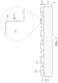
- FIG. 1 shows a reticle-masking structure 10 in accordance with some embodiments of the present disclosure.
- the reticle-masking structure 10 includes a magnetic substrate 101 and a paramagnetic part 103 .
- the magnetic substrate 101 has a magnetic field.
- the paramagnetic part 103 is disposed on the magnetic substrate 101 and has an induced magnetic field having a direction matching that of the magnetic field of the magnetic substrate 101 .
- the paramagnetic part 103 includes a rough surface 103 a and a planar surface 103 b opposite to the rough surface 103 a .
- the paramagnetic part 103 includes a plurality of protrusion structures 1031 .
- a shape of the plurality of protrusion structures 1031 is not limited herein.
- the plurality of protrusion structures is in a pillar shape (as shown in FIG. 1 ), a pyramid shape, a cone shape, a frustum shape, and/or a scallop (curved) shape.
- the plurality of protrusion structures 1031 are proximal to the rough surface 103 a and define the rough surface 103 a .
- the magnetic substrate 101 is disposed on the planar surface 103 b of the paramagnetic part 103 .
- the paramagnetic part 103 is attracted by the magnetic field of the magnetic substrate 101 , and an induced magnetic field in the direction of the magnetic field of the magnetic substrate 101 is formed in the paramagnetic part 103 .
- the paramagnetic part 103 is attached to or bonded on the magnetic substrate 101 by one or more of screwing, gluing, welding, electroplating and magnetic attraction.
- the magnetic substrate 101 and the paramagnetic part 103 are both made of stainless steel, because stainless steel exhibits good absorptance of EUV light.
- the paramagnetic part 103 is made of stainless steel, and the magnetic substrate 101 includes other suitable magnetic materials.
- the paramagnetic part 103 overlaps the entire magnetic substrate 101 .
- the paramagnetic part 103 has a width W 103 substantially equal to a width W 101 of the magnetic substrate 101 .
- the width W 103 of the paramagnetic part 103 is greater than the width W 101 of the magnetic substrate 101 as long as the magnetic field of the magnetic substrate 101 is strong enough to form the induced magnetic field in the entire paramagnetic part 103 .
- a thickness T 101 of the magnetic substrate 101 is in a range of 1 to 20 millimeters for good attractions of the magnetic substrate 101 to the paramagnetic part 103 .
- a thickness T 103 of the paramagnetic part 103 is in a range of 100 micrometers to 5 millimeters. In some embodiments, if the thickness T 103 is smaller than 100 micrometers, it increases the difficulty of fabrication. In some embodiments, if the thickness T 103 is greater than 5 millimeters, it increases manufacturing cost with less improvement.
- the protrusion structures 1031 are regularly arranged, as shown in FIG. 1 .
- the reticle-masking structure 10 further includes an adhesion layer between the magnetic substrate 101 and the paramagnetic part 103 . In some embodiments, the reticle-masking structure 10 further includes one or more screws connecting the paramagnetic part 103 and the magnetic substrate 101 .
- a pitch P 1031 between adjacent protrusion structures 1031 is in a range of 50 nanometers to 500 micrometers, wherein the pitch P 1031 is defined by a distance between centers of the adjacent protrusion structures 1031 , as shown in FIG. 1 . In some embodiments with the pitch of the protrusion structures 1031 out of the range 50 nanometers to 500 micrometers, the results of light diffusion and light trapping are worse.
- a top of the protrusion structure 1031 is in a rounded configuration instead of a rectangular configuration.
- the paramagnetic part 103 of the reticle-masking structure 10 further includes a plurality of fractions 1032 disposed on the protrusion structures 1031 , as shown in an enlarged view of a portion of the paramagnetic part 103 shown in the dotted circle in FIG. 1 .
- the fractions 1032 are paramagnetic materials same as the material of the paramagnetic part 103 .
- the fractions 1032 are pillar-like, irregular, micro-branch, or micro-bulge paramagnetic fractions.
- the fractions 1032 are paramagnetic particles.
- the paramagnetic particles have rounded and/or irregular configurations.
- some of the fractions 1032 and the protrusion structure 1031 are monolithic. In some embodiments, some of the fractions 1032 attached on the protrusion structure 1031 by magnetic attraction and Van der Waals forces. In some embodiments, the plurality of fractions 1032 is not a designed structure in the manufacturing process, and a dimension of the plurality of fractions 1032 is smaller than a dimension of the protrusion structure 1031 . In some embodiments, a diameter D 1032 of the plurality of fractions 1032 is less than 1 micron.
- a material of the paramagnetic part 103 includes stainless steel having a non-face-centered cubic structure. In some embodiments, a material of the paramagnetic part 103 is selected from the group consisting of ferritic stainless steel, martensite stainless steel, precipitation-hardened stainless steel, and duplex stainless steel. In some embodiments, a material of the magnetic substrate 101 includes stainless steel, aluminum, nickel, iron, chromium, neodymium, boron, samarium, cobalt, or an alloy thereof. In some embodiments, the magnetic substrate 101 is one or more of neodymium magnet (NdFeB magnet), samarium-cobalt (SmCo) magnet, and ferrite magnet. In some embodiments, the materials of the paramagnetic part 103 and the magnetic substrate 101 are different. In some embodiments, the materials of the paramagnetic part 103 and the magnetic substrate 101 are the same.
- the magnetic substrate 101 is a permanent magnet. In some embodiments, the magnetic substrate 101 includes ferromagnetic materials with high magnetic coercivity (i.e., magnetically “hard” materials). In some embodiments, the magnetic substrate 101 is an electromagnet, including a coil of wires and a core of ferromagnetic materials with low coercivity (i.e., magnetically “soft” materials). In some embodiments, the magnetic substrate 101 is electrically connected to a power supply or a current generator. In some embodiments, the magnetic substrate 101 is electrically connected to the power supply or the current generator through a wire.
- the protrusion structures 1031 are irregularly arranged.
- FIG. 2 shows a reticle-masking structure 20 in accordance with some embodiments of the present disclosure.
- a plurality of protrusion structures 1031 of a paramagnetic part 103 having different heights and different diameters are disposed on a magnetic substrate 101 .
- the protrusion structures 1031 are irregularly arranged, and some of the protrusion structures 1031 are separated from adjacent protrusion structures 1031 , while others of the protrusion structures 1031 contact adjacent protrusion structures 1031 .
- a top of the protrusion structure 1031 is in a rounded configuration instead of a rectangular configuration.
- the protrusion structures 1031 of the reticle-masking structure 20 are formed by a technique different from a technique used in formation of the protrusion structures 1031 of the reticle-masking structure 10 .
- the paramagnetic part 103 of the reticle-masking structure 20 may further include a plurality of fractions 1032 similar to the fractions 1032 of the reticle-masking structure 10 . Detailed formation of the reticle-masking structures 10 and 20 are illustrated in the following description.
- FIG. 3 shows a flowchart of a method M 10 for forming a reticle-masking structure.
- the method M 10 includes steps of: (O 101 ) receiving a magnetic substrate; (O 102 ) disposing a paramagnetic part on the magnetic substrate; and (O 103 ) removing a portion of the paramagnetic part to form a rough surface of the paramagnetic part. It should be noted that the operations O 101 , O 102 and O 103 of the method M 10 may be rearranged in sequence or otherwise modified within the scope of the various aspects.
- FIG. 4 shows a cross-sectional diagram in accordance with some embodiments of the present disclosure and the operation O 101 of the method M 10 .
- a magnetic substrate 101 is received.
- a paramagnetic part 103 is also received.
- the paramagnetic part 103 is processed to form a rough surface 103 a prior to disposing the paramagnetic part 103 on the magnetic substrate 101 , as shown in FIGS. 5 to 7 and FIGS. 8 to 10 .
- a paramagnetic part 103 is formed on the magnetic substrate 101 prior to formation of the rough surface 103 a , as shown in FIGS. 11 to 13 .
- FIGS. 5 and 6 are cross-sectional diagrams in accordance with some embodiments of the present disclosure and the operation O 103 of the method M 10 .
- a patterned mask layer PM is formed on the paramagnetic part 103 received in the operation O 101 , and a portion of the paramagnetic part 103 exposed through the patterned mask layer PM is removed by a process ET.
- the process ET includes a wet etching operation.
- the process ET includes a plasma dry etching operation.
- the process ET includes a laser etching.
- FIG. 5 is cross-sectional diagrams in accordance with some embodiments of the present disclosure and the operation O 103 of the method M 10 .
- the pattern of the patterned mask layer PM is transferred to the paramagnetic part 103 to form a plurality of protrusion structures 1031 and a rough surface 103 a , wherein the plurality of protrusion structures 1031 define the rough surface 103 a .
- a pattern of the rough surface 103 a is designed or predetermined, and the pattern of the rough surface 103 a is regulated.
- pitches P 1031 between adjacent protrusion structures 1031 are consistent among the plurality of protrusion structures 1031 .
- the pitches P 1031 between adjacent protrusion structures 1031 vary among the protrusion structures 1031 .
- a height H 1031 of the protrusion structure 1031 is smaller than a thickness T 103 of the paramagnetic part 103 . In some embodiments, the heights H 1031 of the protrusion structures 1031 are similar or substantially the same.
- branch-like, bulge-like, pillar-like or irregular residues, fractions, micro branches, and/or micro bulges of the paramagnetic part 103 are formed on the plurality of protrusion structures 1031 during removal of the portion of the paramagnetic part 103 .
- a cleaning operation or a surface treatment is performed after the removal operation of the portion of the paramagnetic part 103 , and some of the residues, fractions, branches and/or bulges are removed by the cleaning operation.
- the fractions 1032 are pillar-like, irregular, micro-branch, or micro-bulge paramagnetic fractions formed on the rough surface 103 a during formation of the rough surface 103 a and remained after the cleaning operation.
- the fractions 1032 are paramagnetic particles formed from cracking of the pillar-like or irregular paramagnetic fractions, micro branches, or micro bulges during cleaning operations or surface treatments.
- connections or adhesions between the rough surface 103 a and fractions 1032 are tenuous, and the fractions 1032 at this stage are easily to separate from the rough surface 103 a if applied in an EUV lithographic operation.
- FIG. 7 is a cross-sectional diagram in accordance with some embodiments of the present disclosure and shows the operation O 102 of the method M 10 applied to the paramagnetic part 103 of FIG. 6 .
- the paramagnetic part 103 with the rough surface 103 a , is disposed on the magnetic substrate 101 to form a reticle-masking structure 11 similar to the reticle-masking structure 10 .
- the regular protrusion structures 1031 are configured to trap EUV radiation beams between the protrusion structures 1031 .
- another cleaning operation is performed after disposing the paramagnetic part 103 on the magnetic substrate 101 .
- FIGS. 8 to 11 are cross-sectional diagrams in accordance with some embodiments of the present disclosure, wherein the operation O 103 is performed prior to the operation O 102 , and the sandblasting operation is performed to form an irregular rough surface 103 a of a paramagnetic part 103 .
- FIGS. 8 to 9 are cross-sectional diagrams in accordance with some embodiments of the present disclosure, and show the operation O 103 of the method M 10 .
- the paramagnetic part 103 received in the operation O 101 is subjected to a sandblasting operation SB. Particles hit a top surface of the paramagnetic part 103 to form the rough surface 103 a with an irregular pattern.
- a plurality of protrusion structures 1031 with an irregular arrangement may be formed, wherein the protrusion structures 1031 can include different heights, different widths, and different shapes.
- the protrusion structures 1031 include a protrusion structure 1031 a and a protrusion structure 1031 b adjacent to each other.
- the protrusion structure 1031 a has a height H 1031 a and a width W 1031 a
- the protrusion structure 1031 b has a height H 1031 b and a width W 1031 b
- the protrusion structure 1031 a and the protrusion structure 1031 b are side by side and in contact with each other.
- the height H 1031 a of the protrusion structure 1031 a is less than the height H 1031 b of the protrusion structure 1031 b
- the width W 1031 a of the protrusion structure 1031 a is less than the width W 1031 b of the protrusion structure 1031 b .
- configurations of the protrusion structures 1031 are different, as shown in an enlarged view of a portion of the paramagnetic part 103 as shown on the left side of FIG. 9 .
- heights of the protrusion structures 1031 are smaller than a thickness T 103 of the paramagnetic part 103 .
- FIG. 10 is a cross-sectional diagram in accordance with some embodiments of the present disclosure and shows the operation O 102 of the method M 10 applied to the paramagnetic part 103 of FIG. 9 .
- the paramagnetic part 103 with the irregular rough surface 103 a , is disposed on the magnetic substrate 101 to form the reticle-masking structure 21 similar to the reticle-masking structure 20 .
- the irregular protrusion structures 1031 are configured to diffuse EUV radiation beams.
- the operation O 102 is performed prior to the operation O 103 .
- the operation O 102 is performed.
- a paramagnetic part 103 is disposed on the magnetic substrate 101 .
- the paramagnetic part 103 includes a planar surface 103 b (bottom surface), and the magnetic substrate 101 is proximal to the planar surface 103 b of the paramagnetic part 103 .
- the paramagnetic part 103 is received as illustrated in FIG. 4 and relevant descriptions thereof, and then the paramagnetic part 103 is disposed on the magnetic substrate 101 .
- the paramagnetic part 103 is attached to or bonded on the magnetic substrate 101 using one or more screws, an adhesive layer or a glue layer. In some embodiments, the paramagnetic part 103 is attached to or bonded on the magnetic substrate 101 by welding. In some embodiments, the paramagnetic part 103 is attached to the magnetic substrate 101 by magnetic attraction. In some embodiments, the paramagnetic part 103 is formed on the magnetic substrate 101 by electroplating or deposition.
- the operation O 103 is performed on the structure shown in FIG. 11 .
- a patterned mask layer PM is formed and a process ET is performed to form a rough surface 103 a of the paramagnetic part 103 .
- a reticle-masking structure 12 is thereby formed, as shown in FIG. 13 .
- a sandblasting operation SB is performed to form a rough surface 103 a with an irregular pattern.
- some of protrusion structures 1031 have a rounded top, as shown in FIG. 13 .
- some of the protrusion structures 1031 have relatively planar tops, and configurations of the protrusion structures 1031 are not limited herein.
- heights H 1031 of the protrusion structures 103 are smaller than a thickness T 103 of the paramagnetic part 103 .
- the fractions 1032 become a plurality of magnets after the paramagnetic part 103 is attached to the magnetic substrate 101 .
- the fractions 1032 may temporarily include magnetic poles with different polarities after the fractions 1032 separate from the rough surface during the EUV operation.
- a top surface 101 a of the magnetic substrate 101 is attached to and entirely covered by the planar surface 103 b of the paramagnetic part 103 .
- the magnetic substrate 101 provides a magnetic field strong enough to create an induced magnetic field in the paramagnetic part 103 , wherein the induced magnetic field is strong enough to attract separated fractions 1032 .
- strength of the magnetic field of the magnetic substrate depends on a thickness of the paramagnetic part 103 and on a quantity of protrusion structures 1031 of the paramagnetic part 103 . In some embodiments, the strength of the magnetic field is greater than 1000 G.
- the magnetic substrate 101 includes one magnet. In some embodiments, the magnetic substrate 101 includes multiple magnets, wherein one magnet includes one south magnetic pole and one north magnetic pole.
- a quantity of protrusion structures 1031 of the paramagnetic part 103 covered by one magnetic field depend on strength of the magnetic field and difficulty of fabricating the magnetic substrate 101 with a certain arrangement of the magnetic field(s). In some embodiments, a number of the protrusion structures 1031 of the paramagnetic part 103 covered by one magnetic field is in a range of 6-6000.
- FIGS. 14 to 17 and FIGS. 20 to 22 are cross-sectional views and FIGS. 18 to 19 are bottom views of different reticle-masking structures in accordance with different embodiments of the present disclosure.
- a rough surface 103 a of a paramagnetic part 103 having a designed pattern is used for a purpose of illustration, but the illustration is not intended to limit the present disclosure.
- a magnetic substrate 101 of a reticle-masking structure 30 includes one magnet.
- the lines with arrows illustrate magnetic field lines and the directions of the magnetic field.
- a paramagnetic part 103 is within the magnetic field of the magnetic substrate 101 , and a magnetic field is induced with a direction matching that of the magnetic field of the magnetic substrate 101 .
- the direction of the magnetic field of the magnetic substrate 101 is from the north magnetic pole to the south magnetic pole.
- an arrangement of a north magnetic pole (hereinafter “N pole”) and a south magnetic pole (hereinafter “S pole”) of the magnet of the magnetic substrate 101 is substantially parallel to a planar surface 103 a of the paramagnetic part 103 .
- the arrangement of the N pole and the S pole is substantially parallel to the lengthwise direction of the paramagnetic part 103 .
- both the N pole and the S pole are in contact with the paramagnetic part 103 .
- magnetic field lines of magnetic substrates 101 in the embodiments shown in FIGS. 15 to 20 are simplified.
- a magnetic substrate 101 of a reticle-masking structure 31 also includes one magnet, but the direction of the arrangement of the N pole and the S pole in the reticle-masking structure 31 is different from that in the reticle-masking structure 30 .
- only one of the N pole and the S pole is in contact with the paramagnetic part 103 .
- the arrangement of the N pole and the S pole is substantially perpendicular to the planar surface 103 a of the paramagnetic part 103 .
- the arrangement of the N pole and the S pole is substantially perpendicular to the lengthwise direction of the paramagnetic part 103 .
- a sidewall S 1011 of an edge magnet 1011 is aligned with a sidewall S 103 of the paramagnetic part 103 .
- a magnetic substrate 101 of a reticle-masking structure 32 includes a plurality of magnets 1011 .
- a paramagnetic part 103 is within magnetic fields of the magnetic substrate 101 , and a plurality of magnetic fields is induced with directions matching those of the magnetic fields of the magnets 1011 of the magnetic substrate 101 .
- each of the magnets 1011 contacts an adjacent magnet 1011 .
- an N pole of a magnet 1011 contacts an S pole of the adjacent magnet 1011 .
- a width W 101 of the magnetic substrate 101 is less than a width W 103 of the paramagnetic part 103 .
- an arrangement of the N pole and the S pole of each of the magnets 1011 is substantially parallel to a planar surface 103 b of the paramagnetic part 103 . In some embodiments, the arrangement of the N pole and the S pole of each of the magnets 1011 is substantially parallel to a lengthwise direction of the paramagnetic part 103 . In some embodiment, a sidewall S 1011 of an edge magnet 1011 is not aligned with a sidewall S 103 of the paramagnetic part 103 depends on strengths of the magnetic fields of the substrate 101 . In some embodiments, all magnets 1011 are within an area of the planar surface 103 b of the paramagnetic part 103 .
- a magnetic substrate 101 of a reticle-masking structure 33 includes a plurality of magnets 1011 , similar to the magnetic substrate 101 of the reticle-masking structure 32 .
- a difference between the reticle-masking structure 33 and the reticle-masking structure 32 is that the magnets 1011 of the reticle-masking structure 33 are separated from each other.
- the magnets 1011 are embedded in or bonded by a material structure 1012 to make the magnets 1011 and the material structure 1012 as a one-piece magnetic substrate 101 .
- a size and shape of the material structure 1012 is not limited herein as long as the material structure 1012 can connect all the magnets 1011 to form a plate-like substrate.
- the material structure 1012 is made of dielectric materials without blocking the magnetic attractions of the magnets. Magnetic fields between the magnets 1011 induce magnetic fields in the paramagnetic part 103 .
- FIGS. 18 and 19 are bottom views of a portion of the reticle-masking structure 33 in accordance with different embodiments.
- the magnets 1011 are all in a strip or a rectangular configuration, and the magnets 1011 are arranged parallel to each other.
- the plurality of magnets 1011 are arranged along a direction perpendicular to a lengthwise direction of each of the magnets.
- the plurality of magnets 1011 extends along X direction while an extending direction of a single magnet 1011 is along Y direction According to some embodiments, FIG.
- FIG. 17 shows the reticle-masking structure 33 from a cross-sectional perspective taken along a line A-A′ in FIG. 18 .
- each of the magnets 1011 is smaller than the magnet 1011 shown in FIG. 18 , and an arrangement of the magnets 1011 or a pattern of the magnetic substrate 101 is in a grid array, as shown in FIG. 19 .
- the plurality of magnets 1011 is arranged to extend in both the X direction and the Y direction.
- FIG. 17 shows the reticle-masking structure 33 from a cross-sectional perspective taken along a line B-B′ in FIG. 19 .
- FIG. 17 shows the reticle-masking structure 33 from a cross-sectional perspective taken along a line C-C′ in FIG. 19 .
- the material structure 1012 is entirely covered by and smaller than the paramagnetic part 103 .
- the present disclosure is not limited herein.
- material structure 1012 is entirely overlapped and substantially the same size as the paramagnetic part 103 .
- FIG. 20 shows a magnetic substrate 101 of a reticle-masking structure 34 similar to the magnetic substrate 101 of the reticle-masking structure 33 .
- a difference between the reticle-masking structure 34 and the reticle-masking structure 33 is that the arrangement of the N pole and the S pole of each magnet 1011 is substantially perpendicular to the rough surface 103 a of the paramagnetic part 103 .
- the arrangement of the N pole and the S pole of each magnet 1011 is substantially perpendicular to a lengthwise direction of the paramagnetic part 103 .
- magnetic field directions of adjacent magnets 1011 are opposite.
- the magnets 1011 or the magnetic substrate 101 on the paramagnetic part 103 of the reticle-masking structure 34 as shown in 20 are arranged in a plurality of parallel strips similar to the bottom view shown in FIG. 18 . In some embodiments, the magnets 1011 or the magnetic substrate 101 on the paramagnetic part 103 of the reticle-masking structure 34 as shown in FIG. 20 are arranged as a grid array similar to the bottom view shown in FIG. 19 .
- FIG. 21 shows a magnetic substrate 101 of a reticle-masking structure 35 similar to the magnetic substrate 101 of the reticle-masking structure 34 .
- a difference between the reticle-masking structure 35 and the reticle-masking structure 34 is that in the reticle-masking structure 35 , magnets 1011 are in contact with adjacent magnets 1011 instead of being separated from each other. In some embodiments, the N poles and the S poles of the magnets 1011 are alternately arranged.
- Magnetic field lines of the reticle-masking structure 35 are similar to those of the reticle-masking structure 34 shown in FIG. 20 , and for ease of illustration, magnetic field lines are omitted in FIG. 23 .
- FIG. 22 shows a magnetic substrate 101 of a reticle-masking structure 36 similar to the magnetic substrate 101 of the reticle-masking structure 35 .
- a difference between the reticle-masking, structure 36 and the reticle-masking structure 35 is that in the reticle-masking structure 36 , same polarities of adjacent magnets 1011 are aligned.
- the N poles of the magnets 1011 are in contact with the paramagnetic part 103 and an N pole of a magnet 1011 is in contact a N pole of an adjacent magnets 1011 , as shown in FIG. 22 .
- the S poles of the magnets 1011 are in contact with the paramagnetic part 103 .
- Magnetic field lines of the reticle-masking structure 36 are similar to those of the reticle-masking structure 31 shown in FIG. 15 , and for ease of illustration, magnetic field lines are omitted in FIG. 24 .
- an EUV apparatus including one of the above illustrated reticle-masking structures.
- an EUV apparatus A 10 in accordance with some embodiments of the present disclosure is provided.
- the EUV apparatus A 10 includes a radiation source 210 , a reticle-masking structure 10 , and a reticle 220 .
- the radiation source 210 is configured to generate a radiation beam 211 (e.g., EUV rays).
- the reticle-masking structure 10 is replaced by one of the above-described reticle-masking structures 11 , 12 , 20 , 21 , or 30 to 36 .
- the reticle-masking structure 10 is used herein for a purpose of illustration, but is not intended to limit the present disclosure.
- the reticle-masking structure is configured to diffuse a portion of the radiation beam 211 .
- the reticle 220 is configured to reflect the remaining portion of the radiation beam after the diffusion of the portion of the radiation beam in order to transfer a pattern of the reticle 220 onto a wafer 300 .
- the apparatus A 10 further includes an optical collector 212 , configured to concentrate the radiation beam 211 generated by the radiation source 210 onto the reticle 220 .
- the apparatus A 10 further includes an optical system 240 , configured to receive the radiation beam 211 from the radiation source 210 and reflect the radiation beam 211 onto the reticle 220 and then onto the wafer 300 .
- the optical system 240 includes a plurality of mirrors 241 , configured to reflect the radiation beam 211 from the radiation source 210 toward the reticle 220 .
- the plurality of mirrors 241 are also configured to reduce a size of the pattern of the reticle 220 and reflect the radiation beam 211 onto the wafer 300 .
- the plurality of mirrors 241 include a plurality of plane mirrors 241 a to reflect the radiation beam 211 from the radiation source 210 toward the reticle 220 .
- the plurality of mirrors 241 include a plurality of concave mirrors 241 b configured to concentrate the radiation beam 211 reflected by the reticle 220 in order to reduce the size of the pattern of the reticle 220 .
- the apparatus A 10 further includes a reticle stage 230 configured to load or carry the reticle 220 .
- the apparatus A 10 further includes a masking carrier 231 , configured to load or carry the reticle-masking structure 10 .
- the masking carrier 231 includes a motor (not shown), configured to adjust a position of the reticle-masking structure 10 .
- the apparatus A 10 further includes a wafer stage 232 , configured to load or carry the wafer 300 .
- the wafer stage 232 includes a motor (not shown), configured to adjust a position of the wafer 300 .
- FIGS. 24 to 25 show an enlarged view of a portion (indicated with a dashed-line box in FIG. 23 ) of the apparatus A 10 during an EUV lithographic operation performed by the apparatus A 10 in accordance with different embodiments.
- the radiation beam 211 from the radiation source 210 includes a first portion 2111 and a second portion 2112 .
- the first portion 2111 is a portion of the radiation beam 211 that is to be prevented from irradiating the wafer 300 .
- the first portion 2111 is radiated onto the rough surface 103 a of the reticle-masking structure 10 and is diffused by the rough surface 103 a .
- the radiation beam 211 (e.g., EUV light) gives energy to the fractions 1032 , causing the fractions 1032 to separate from the rough surface 103 a , after the reticle-masking structure 10 being irradiated by the first portion 2111 of the radiation beam 211 .
- the separated fractions 1032 are attracted back to the rough surface 103 a by the magnetic forces of the magnetic substrate 101 and the paramagnetic part 103 .
- the fractions 1032 are attached to the rough surface 103 a of the paramagnetic part 103 by magnetic attraction.
- positions of the fractions 1032 on the rough surface 103 a changes during the EUV lithographic operation.
- the fractions 1032 are remained steadily on the rough surface 103 a of the paramagnetic part 103 by strong magnetic attraction during the EUV lithographic operation.
- the second portion 2112 of the radiation beam 211 is reflected by the reticle 220 .
- the reticle 220 includes a pattern 221
- the pattern 221 includes an edge pattern 221 a and a chip pattern 221 b .
- the second portion 2112 is reflected by a portion of the reticle 220 having the chip pattern 221 b and at least a portion of the edge pattern 221 a .
- an image of the edge pattern 221 a is substantially transferred to a scribe line region of the wafer 300 .
- a first sub-portion 211 a of the second portion 2112 of the radiation beam 211 is reflected by a portion of the reticle 220 having the edge pattern 221 a .
- the chip pattern 221 b may correspond to a layout pattern constituting integrated circuits.
- an image of the chip pattern 221 b is transferred to a die region of the wafer 300 .
- a second sub-portion 211 b of the second portion 2112 of the radiation beam 211 is reflected by a portion of the reticle 220 having the chip pattern 221 b.
- the radiation beam 211 from the radiation source 210 includes a first portion 2111 and a second portion 2112 , wherein the rough surface 103 a of the reticle-masking structure 10 helps to diffuses the first portion 2111 so that the reflection of the first portion 2111 is reduced.
- the second portion 2112 is reflected by the reticle 220 , particularly by the chip pattern 221 b .
- a difference between the embodiments shown in FIG. 27 and the embodiments shown in FIG. 24 is that, in the embodiments shown in FIG. 27 , the second portion 2112 is substantially reflected by a portion of the reticle 220 having substantially the chip pattern 221 b .
- the radiation beam 211 further includes a penumbra portion 2113 after the radiation beam 211 is radiated onto the reticle-masking structure 10 .
- the penumbra portion 2113 is projected onto a portion of the reticle 220 having the edge pattern 221 a .
- a light intensity of the penumbra portion 2113 is very low, and the penumbra portion 2113 is not able to transfer an image of the edge pattern 221 a onto the wafer 300 .
- the penumbra portion 2113 is reflected by the portion of the reticle 220 having the edge pattern 221 a.
- the reticle-masking structure includes a magnetic substrate and a paramagnetic part disposed on the magnetic substrate.
- the paramagnetic part includes a plurality of fractions disposed on a plurality of protrusion structures. In some embodiments, the plurality of fractions are irregularly arranged.
- Some embodiments of the present disclosure provide a method for forming a reticle-masking structure.
- the method includes: receiving a magnetic substrate; disposing a paramagnetic part on the magnetic substrate; removing a portion of the paramagnetic part to form a rough surface; and forming a plurality of fractions on the rough surface.
- the plurality of fractions are irregularly arranged.
- the extreme ultraviolet apparatus includes: a radiation source, a reticle-masking structure and a reticle.
- the radiation source generates a radiation beam
- the reticle-masking structure is configured to diffuse the radiation beam.
- the reticle-masking structure includes a magnetic substrate and a paramagnetic part disposed on the magnetic substrate.
- the paramagnetic part includes a plurality of fractions irregularly arranged on a surface of the paramagnetic part.
- the reticle is configured to reflect the radiation beam.
Landscapes
- Physics & Mathematics (AREA)
- General Physics & Mathematics (AREA)
- Health & Medical Sciences (AREA)
- Epidemiology (AREA)
- Public Health (AREA)
- Engineering & Computer Science (AREA)
- Life Sciences & Earth Sciences (AREA)
- Atmospheric Sciences (AREA)
- Environmental & Geological Engineering (AREA)
- Plasma & Fusion (AREA)
- Exposure And Positioning Against Photoresist Photosensitive Materials (AREA)
Abstract
Description
Claims (20)
Priority Applications (1)
| Application Number | Priority Date | Filing Date | Title |
|---|---|---|---|
| US17/704,309 US12066760B2 (en) | 2019-10-01 | 2022-03-25 | Reticle-masking structure, extreme ultra violet apparatus, and method of forming the same |
Applications Claiming Priority (3)
| Application Number | Priority Date | Filing Date | Title |
|---|---|---|---|
| US16/589,616 US10866519B1 (en) | 2019-10-01 | 2019-10-01 | Reticle-masking structure, extreme ultraviolet apparatus, and method of forming the same |
| US17/121,588 US11287745B2 (en) | 2019-10-01 | 2020-12-14 | Reticle-masking structure, extreme ultraviolet apparatus, and method of forming the same |
| US17/704,309 US12066760B2 (en) | 2019-10-01 | 2022-03-25 | Reticle-masking structure, extreme ultra violet apparatus, and method of forming the same |
Related Parent Applications (1)
| Application Number | Title | Priority Date | Filing Date |
|---|---|---|---|
| US17/121,588 Continuation US11287745B2 (en) | 2019-10-01 | 2020-12-14 | Reticle-masking structure, extreme ultraviolet apparatus, and method of forming the same |
Publications (2)
| Publication Number | Publication Date |
|---|---|
| US20220214620A1 US20220214620A1 (en) | 2022-07-07 |
| US12066760B2 true US12066760B2 (en) | 2024-08-20 |
Family
ID=73747001
Family Applications (3)
| Application Number | Title | Priority Date | Filing Date |
|---|---|---|---|
| US16/589,616 Active US10866519B1 (en) | 2019-10-01 | 2019-10-01 | Reticle-masking structure, extreme ultraviolet apparatus, and method of forming the same |
| US17/121,588 Active US11287745B2 (en) | 2019-10-01 | 2020-12-14 | Reticle-masking structure, extreme ultraviolet apparatus, and method of forming the same |
| US17/704,309 Active US12066760B2 (en) | 2019-10-01 | 2022-03-25 | Reticle-masking structure, extreme ultra violet apparatus, and method of forming the same |
Family Applications Before (2)
| Application Number | Title | Priority Date | Filing Date |
|---|---|---|---|
| US16/589,616 Active US10866519B1 (en) | 2019-10-01 | 2019-10-01 | Reticle-masking structure, extreme ultraviolet apparatus, and method of forming the same |
| US17/121,588 Active US11287745B2 (en) | 2019-10-01 | 2020-12-14 | Reticle-masking structure, extreme ultraviolet apparatus, and method of forming the same |
Country Status (3)
| Country | Link |
|---|---|
| US (3) | US10866519B1 (en) |
| CN (1) | CN112596336A (en) |
| TW (1) | TW202115771A (en) |
Families Citing this family (1)
| Publication number | Priority date | Publication date | Assignee | Title |
|---|---|---|---|---|
| US10866519B1 (en) * | 2019-10-01 | 2020-12-15 | Taiwan Semiconductor Manufacturing Company Ltd. | Reticle-masking structure, extreme ultraviolet apparatus, and method of forming the same |
Citations (4)
| Publication number | Priority date | Publication date | Assignee | Title |
|---|---|---|---|---|
| US20050275835A1 (en) * | 2004-06-15 | 2005-12-15 | Nikon Corporation | Method and apparatus for protecting an EUV reticle from particles |
| US20060073395A1 (en) * | 2004-10-01 | 2006-04-06 | Nikon Corporation, A Japanese Corporation | Contact material and system for ultra-clean applications |
| US20170212428A1 (en) * | 2014-10-07 | 2017-07-27 | Carl Zeiss Smt Gmbh | Vacuum linear feed-through and vacuum system having said vacuum linear feed-through |
| US10866519B1 (en) * | 2019-10-01 | 2020-12-15 | Taiwan Semiconductor Manufacturing Company Ltd. | Reticle-masking structure, extreme ultraviolet apparatus, and method of forming the same |
Family Cites Families (16)
| Publication number | Priority date | Publication date | Assignee | Title |
|---|---|---|---|---|
| US6544693B2 (en) * | 2001-01-26 | 2003-04-08 | Advanced Micro Devices, Inc. | Pellicle for use in small wavelength lithography and a method for making such a pellicle |
| EP1482363A1 (en) * | 2003-05-30 | 2004-12-01 | ASML Netherlands B.V. | Lithographic apparatus |
| US7119883B2 (en) * | 2004-10-13 | 2006-10-10 | Asml Holding N.V. | Correcting variations in the intensity of light within an illumination field without distorting the telecentricity of the light |
| US8764995B2 (en) | 2010-08-17 | 2014-07-01 | Taiwan Semiconductor Manufacturing Company, Ltd. | Extreme ultraviolet light (EUV) photomasks, and fabrication methods thereof |
| DE102011075465B4 (en) * | 2011-05-06 | 2013-09-12 | Carl Zeiss Smt Gmbh | Projection objective of a microlithographic projection exposure apparatus |
| NL2008845A (en) * | 2011-05-24 | 2012-11-27 | Asml Netherlands Bv | Lithographic apparatus and component. |
| US8841047B2 (en) | 2012-04-02 | 2014-09-23 | Taiwan Semiconductor Manufacturing Company, Ltd. | Extreme ultraviolet lithography process and mask |
| US8877409B2 (en) | 2012-04-20 | 2014-11-04 | Taiwan Semiconductor Manufacturing Company, Ltd. | Reflective mask and method of making same |
| US8828625B2 (en) | 2012-08-06 | 2014-09-09 | Taiwan Semiconductor Manufacturing Company, Ltd. | Extreme ultraviolet lithography mask and multilayer deposition method for fabricating same |
| US9093530B2 (en) | 2012-12-28 | 2015-07-28 | Taiwan Semiconductor Manufacturing Company, Ltd. | Fin structure of FinFET |
| US8796666B1 (en) | 2013-04-26 | 2014-08-05 | Taiwan Semiconductor Manufacturing Company, Ltd. | MOS devices with strain buffer layer and methods of forming the same |
| US9548303B2 (en) | 2014-03-13 | 2017-01-17 | Taiwan Semiconductor Manufacturing Company, Ltd. | FinFET devices with unique fin shape and the fabrication thereof |
| US9529268B2 (en) | 2014-04-03 | 2016-12-27 | Taiwan Semiconductor Manufacturing Company, Ltd. | Systems and methods for improving pattern transfer |
| US9256123B2 (en) | 2014-04-23 | 2016-02-09 | Taiwan Semiconductor Manufacturing Co., Ltd. | Method of making an extreme ultraviolet pellicle |
| US9184054B1 (en) | 2014-04-25 | 2015-11-10 | Taiwan Semiconductor Manufacturing Company, Ltd. | Method for integrated circuit patterning |
| US10871721B2 (en) * | 2018-09-28 | 2020-12-22 | Taiwan Semiconductor Manufacturing Co., Ltd. | Mask blank for lithography and method of manufacturing the same |
-
2019
- 2019-10-01 US US16/589,616 patent/US10866519B1/en active Active
-
2020
- 2020-04-16 TW TW109112869A patent/TW202115771A/en unknown
- 2020-04-30 CN CN202010362158.9A patent/CN112596336A/en active Pending
- 2020-12-14 US US17/121,588 patent/US11287745B2/en active Active
-
2022
- 2022-03-25 US US17/704,309 patent/US12066760B2/en active Active
Patent Citations (5)
| Publication number | Priority date | Publication date | Assignee | Title |
|---|---|---|---|---|
| US20050275835A1 (en) * | 2004-06-15 | 2005-12-15 | Nikon Corporation | Method and apparatus for protecting an EUV reticle from particles |
| US20060073395A1 (en) * | 2004-10-01 | 2006-04-06 | Nikon Corporation, A Japanese Corporation | Contact material and system for ultra-clean applications |
| US20170212428A1 (en) * | 2014-10-07 | 2017-07-27 | Carl Zeiss Smt Gmbh | Vacuum linear feed-through and vacuum system having said vacuum linear feed-through |
| US10866519B1 (en) * | 2019-10-01 | 2020-12-15 | Taiwan Semiconductor Manufacturing Company Ltd. | Reticle-masking structure, extreme ultraviolet apparatus, and method of forming the same |
| US11287745B2 (en) * | 2019-10-01 | 2022-03-29 | Taiwan Semiconductor Manufacturing Company Ltd. | Reticle-masking structure, extreme ultraviolet apparatus, and method of forming the same |
Also Published As
| Publication number | Publication date |
|---|---|
| US20220214620A1 (en) | 2022-07-07 |
| TW202115771A (en) | 2021-04-16 |
| CN112596336A (en) | 2021-04-02 |
| US11287745B2 (en) | 2022-03-29 |
| US10866519B1 (en) | 2020-12-15 |
| US20210096469A1 (en) | 2021-04-01 |
Similar Documents
| Publication | Publication Date | Title |
|---|---|---|
| CA2107451C (en) | Electron lithography using photocathode | |
| JP2022174091A (en) | Energy filter element for ion implantation systems used in wafer manufacturing | |
| EP1160824A2 (en) | Illumination system for charged-particle lithography apparatus | |
| US12066760B2 (en) | Reticle-masking structure, extreme ultra violet apparatus, and method of forming the same | |
| US7619233B2 (en) | Light source | |
| TW200540561A (en) | Lithographic apparatus having a debris-mitigation system, a source for producing euv radiation having a debris mitigation system and a method for mitigating debris | |
| CN105372944B (en) | Device for charged particle etching system | |
| JP2000138165A (en) | Charged particle drawing method and charged particle drawing device | |
| US7179570B2 (en) | Chromeless phase shift lithography (CPL) masks having features to pattern large area line/space geometries | |
| TW201351065A (en) | Device with plasma radiation source and method for forming a radiation beam and lithography device | |
| JP2003045789A (en) | Drawing apparatus and drawing method | |
| TWI653509B (en) | Device for shielding a mask | |
| US6165688A (en) | Method of fabricating of structures by metastable atom impact desorption of a passivating layer | |
| EP1343050A2 (en) | Device and system for improving phase shift mask imaging performance and associated methods | |
| US6483117B1 (en) | Symmetric blanking for high stability in electron beam exposure systems | |
| US11817293B2 (en) | Photoresist layers of semiconductor components including electric fields, system, and methods of forming same | |
| JP2014194923A (en) | Electron lens and electron beam device | |
| Bell et al. | Atomic lithography | |
| US20160056046A1 (en) | Method of producing aperture member | |
| WO2025250540A1 (en) | Lithography using spin isolated monochromatic electromagnetic radiation | |
| Ahmed | Physical principles of electron beam lithography | |
| JP3004240B2 (en) | Method of forming through hole and buried pattern, beam adjusting method, and charged beam exposure method | |
| KR100352492B1 (en) | A method of fabrication fine circuit | |
| Merhari et al. | Anisotropic Organic/Inorganic Resists: A Novel Concept for Electron Proximity Effect Reduction | |
| JPS6068538A (en) | X-ray generator |
Legal Events
| Date | Code | Title | Description |
|---|---|---|---|
| FEPP | Fee payment procedure |
Free format text: ENTITY STATUS SET TO UNDISCOUNTED (ORIGINAL EVENT CODE: BIG.); ENTITY STATUS OF PATENT OWNER: LARGE ENTITY |
|
| STPP | Information on status: patent application and granting procedure in general |
Free format text: DOCKETED NEW CASE - READY FOR EXAMINATION |
|
| STPP | Information on status: patent application and granting procedure in general |
Free format text: NON FINAL ACTION MAILED |
|
| STPP | Information on status: patent application and granting procedure in general |
Free format text: RESPONSE TO NON-FINAL OFFICE ACTION ENTERED AND FORWARDED TO EXAMINER |
|
| STPP | Information on status: patent application and granting procedure in general |
Free format text: FINAL REJECTION MAILED |
|
| STPP | Information on status: patent application and granting procedure in general |
Free format text: ADVISORY ACTION MAILED |
|
| STPP | Information on status: patent application and granting procedure in general |
Free format text: DOCKETED NEW CASE - READY FOR EXAMINATION |
|
| STPP | Information on status: patent application and granting procedure in general |
Free format text: NON FINAL ACTION MAILED |
|
| STPP | Information on status: patent application and granting procedure in general |
Free format text: RESPONSE TO NON-FINAL OFFICE ACTION ENTERED AND FORWARDED TO EXAMINER |
|
| STPP | Information on status: patent application and granting procedure in general |
Free format text: NOTICE OF ALLOWANCE MAILED -- APPLICATION RECEIVED IN OFFICE OF PUBLICATIONS |
|
| ZAAA | Notice of allowance and fees due |
Free format text: ORIGINAL CODE: NOA |
|
| ZAAB | Notice of allowance mailed |
Free format text: ORIGINAL CODE: MN/=. |
|
| STPP | Information on status: patent application and granting procedure in general |
Free format text: PUBLICATIONS -- ISSUE FEE PAYMENT VERIFIED |
|
| STCF | Information on status: patent grant |
Free format text: PATENTED CASE |