US12038607B2 - Optical arithmetic unit - Google Patents
Optical arithmetic unit Download PDFInfo
- Publication number
- US12038607B2 US12038607B2 US16/976,866 US201916976866A US12038607B2 US 12038607 B2 US12038607 B2 US 12038607B2 US 201916976866 A US201916976866 A US 201916976866A US 12038607 B2 US12038607 B2 US 12038607B2
- Authority
- US
- United States
- Prior art keywords
- optical
- elements
- light
- output
- port
- Prior art date
- Legal status (The legal status is an assumption and is not a legal conclusion. Google has not performed a legal analysis and makes no representation as to the accuracy of the status listed.)
- Active, expires
Links
Images


Classifications
-
- G—PHYSICS
- G02—OPTICS
- G02B—OPTICAL ELEMENTS, SYSTEMS OR APPARATUS
- G02B6/00—Light guides; Structural details of arrangements comprising light guides and other optical elements, e.g. couplings
- G02B6/10—Light guides; Structural details of arrangements comprising light guides and other optical elements, e.g. couplings of the optical waveguide type
- G02B6/12—Light guides; Structural details of arrangements comprising light guides and other optical elements, e.g. couplings of the optical waveguide type of the integrated circuit kind
- G02B6/122—Basic optical elements, e.g. light-guiding paths
- G02B6/125—Bends, branchings or intersections
-
- G—PHYSICS
- G02—OPTICS
- G02B—OPTICAL ELEMENTS, SYSTEMS OR APPARATUS
- G02B6/00—Light guides; Structural details of arrangements comprising light guides and other optical elements, e.g. couplings
- G02B6/24—Coupling light guides
- G02B6/26—Optical coupling means
- G02B6/28—Optical coupling means having data bus means, i.e. plural waveguides interconnected and providing an inherently bidirectional system by mixing and splitting signals
- G02B6/2804—Optical coupling means having data bus means, i.e. plural waveguides interconnected and providing an inherently bidirectional system by mixing and splitting signals forming multipart couplers without wavelength selective elements, e.g. "T" couplers, star couplers
-
- G—PHYSICS
- G02—OPTICS
- G02F—OPTICAL DEVICES OR ARRANGEMENTS FOR THE CONTROL OF LIGHT BY MODIFICATION OF THE OPTICAL PROPERTIES OF THE MEDIA OF THE ELEMENTS INVOLVED THEREIN; NON-LINEAR OPTICS; FREQUENCY-CHANGING OF LIGHT; OPTICAL LOGIC ELEMENTS; OPTICAL ANALOGUE/DIGITAL CONVERTERS
- G02F3/00—Optical logic elements; Optical bistable devices
- G02F3/02—Optical bistable devices
- G02F3/026—Optical bistable devices based on laser effects
-
- G—PHYSICS
- G02—OPTICS
- G02F—OPTICAL DEVICES OR ARRANGEMENTS FOR THE CONTROL OF LIGHT BY MODIFICATION OF THE OPTICAL PROPERTIES OF THE MEDIA OF THE ELEMENTS INVOLVED THEREIN; NON-LINEAR OPTICS; FREQUENCY-CHANGING OF LIGHT; OPTICAL LOGIC ELEMENTS; OPTICAL ANALOGUE/DIGITAL CONVERTERS
- G02F7/00—Optical analogue/digital converters
Definitions
- the present invention relates to an optical computing unit, such as an optical digital-to-analog convertor (DAC) using optical circuits.
- an optical computing unit such as an optical digital-to-analog convertor (DAC) using optical circuits.
- DAC optical digital-to-analog convertor
- DAC convertors digital-to-analog convertors
- electric circuits have been proposed, which have a different performance in terms of sampling rate, resolution, power consumption, size and the like.
- different types of DACs are selected and used depending on intended use.
- a 1 GS/s sampling rate is regarded as high-speed
- a 16 (B)it or higher resolution is regarded as high resolution.
- Latency (delay) of current high resolution DACs will also be a bottleneck in future.
- An optical computing unit of embodiments of the present invention includes: cascade-connected N number (N is 2 or greater integer) of at least one type of elements out of first Y coupling elements having two inputs and one output of which input is one or two signal lights, and a Y coupling/Y branching element having two inputs and two outputs of which input is one or two signal lights; and N number of optical modulators that individually modulate a continuous light to a second optical input port, which is different from a first optical input port to which no light is input or a first optical input port to which a signal light from an optical output of an element in a previous stage is input, out of two optical input ports of each one of N number of cascade-connected elements, in accordance with corresponding bits of an N-bit electric digital signal, so as to generate signal lights to the second optical input port.
- the output light acquired from the element in the final stage is regarded as the computing result.
- a configuration example of the optical computing unit of embodiments of the present invention includes the N number of first Y coupling elements.
- the N number of first Y coupling elements are cascade-connected so that: (N ⁇ 1) number of first Y coupling elements, not including the first Y coupling element at the most upstream side, enable the lights output from the optical output ports of the first Y coupling elements at the upstream side to be the input lights to the first optical input ports; and the N number of Y coupling elements, including the first Y coupling element at the most upstream side, enable the signal lights modulated by the N number of optical modulators to be the input lights to the second optical input ports.
- the N number of optical modulators individually modulate the N number of continuous lights having the same wavelength, in accordance with the corresponding bits of the N-bit electric digital signal so as to generate signal lights to the second optical input ports of the N number of first Y coupling elements.
- the output light acquired from the first Y coupling element in the final stage is regarded as the N-bit digital analog computing result.
- a configuration example of the optical computing unit of embodiments of the present invention includes the (N ⁇ 1) number of Y coupling/Y branching elements and one first Y coupling element.
- the (N ⁇ 1) number of Y coupling/Y branching elements and one first Y coupling element are cascade-connected so that: an (N ⁇ 2) number of Y coupling/Y branching elements, not including the Y coupling/Y branching element at the most upstream side, and the one first Y coupling element enable the lights output from the first optical output ports of the Y coupling/Y branching elements at the upstream side to be the input lights to the first optical input ports; and the (N ⁇ 1) number of Y coupling/Y branching elements, including the Y coupling/Y branching element at the most upstream side, and the one first Y coupling element enable the signal lights modulated by the N number of optical modulators to be the input light to the second optical input ports.
- the N number of optical modulators individually modulate N number of continuous lights having the same wavelength, in accordance with the corresponding bits of the N-bit electric digital signal so as to generate signal lights to the second optical input ports of the (N ⁇ 1) number of Y coupling/Y branching elements and the second optical input port of the one first Y coupling element.
- the output light acquired from a second optical output port which is different from a first optical output port to output a signal light to an element in the subsequent stage, out of the two optical output ports of each of the (N ⁇ 1) number of Y coupling/Y branching elements, and an output light acquired from the first Y coupling element at the final stage are regarded as the 1 to N-bit digital analog computing result.
- a configuration example of the optical computing unit of embodiments of the present invention includes the N number of Y coupling/Y branching elements.
- the N number of Y coupling/Y branching elements are cascade-connected so that: an (N ⁇ 1) number of Y coupling/Y branching elements, not including the Y coupling/Y branching element at the most upstream side, enable the lights output from the first optical output ports of the Y coupling/Y branching elements at the upstream side to be the input lights to the first optical input ports; and the N number of Y coupling/Y branching elements, including the Y coupling/Y branching element at the most upstream side, enable the signal lights modulated by the N number of optical modulators to be the input lights to the second optical input ports.
- the N number of optical modulators individually modulate N number of continuous lights having the same wavelength, in accordance with the corresponding bits of the N-bit electric digital signal so as to generate signal lights to the second optical input ports of the N number of Y coupling/Y branching elements.
- Cascade-connected (N ⁇ 1) number of second Y coupling elements having two inputs and one output are further included.
- a signal light acquired from a second optical output port which is different from a first optical output port that outputs a signal light to the Y coupling/Y branching element in the subsequent stage, out of the two optical output ports of the Y coupling/Y branching element in the first stage, is input to the first optical input port of the second Y coupling element in the first stage;
- a signal light acquired from an optical port of the second Y coupling element in the (k ⁇ 1)th stage (k is an integer in a 2 to (N ⁇ 1) range) is input to the first optical input port of the second Y coupling element in the k-th stage;
- a signal light acquired from the second optical output port of the Y coupling/Y branching element in the (j+1)th stage (j is an integer in a 1 to (N ⁇ 1) range) is input to the second optical input port of the second Y coupling element.
- the output light acquired from the first optical output port of the Y coupling/Y branching element in the final stage is regarded as the N-bit digital analog computing result
- the output light acquired from the second Y coupling element in the final stage is regarded as the N-bit counter computing result.
- a configuration example of the optical computing unit of embodiments of the present invention includes the N number of first coupling elements.
- the N number of first Y coupling elements are cascade-connected so that: an (N ⁇ 1) number of first Y coupling elements, not including the first Y coupling element at the most upstream side, enable the lights output from the optical output ports of the first Y coupling elements at the upstream side to be the input lights to the first optical input ports; and the N number of first Y coupling elements, including the first coupling element at the most upstream side, enable the signal lights modulated by the N number of optical modulators to be the input lights to the second optical input ports.
- An N number of Y branching elements having one input and two outputs are further included.
- the N number of Y branching elements are cascade-connected so that each of the Y branching elements, not including the Y branching element at the most upstream side, of which input is a single continuous light, enables the light output from the first optical output port, out of the two optical output ports of the Y branch element at the upstream side to be input.
- the output lights acquired from the second optical output ports of the N number of Y branching elements are enabled to be the input lights to the N number of optical modulators.
- the output light acquired from the first Y coupling element in the final stage is regarded as the N-bit digital analog computing result.
- At least one of the first Y coupling elements or at least one of the Y coupling elements constituting the Y coupling/Y branching elements has a bias port to which a bias light having a fixed intensity is input, besides the first and second optical input ports.
- a configuration example of the optical computing unit of embodiments of the present invention further includes a Y coupling element that enables the output light acquired from the element in the final stage to be the input light to the first optical input port, and enables the bias light having a fixed intensity to be the input light to the second optical input port.
- the output light acquired from this Y coupling element is regarded as the N-th bit digital analog computation.
- the optical modulator is an optical intensity modulator.
- the optical modulator is an optical phase modulator.
- a coherent detection unit that extracts electric signals after the digital analog conversion is further included.
- the coherent detection unit further includes: a phase shifter that adjusts the phase difference between the output light, which is the N-bit digital analog computing result, and the reference light of which wavelength is the same as the output light, to be ⁇ /2; a coupler that couples the output light, which is the N-bit digital analog computing result, and the reference light, equally divides the coupled light into two, and outputs the divided lights; a first photo detector that converts one of the output lights of the coupler into an electric signal; a second photodetector that converts the other of the output lights of the coupler into an electric signal; and a subtracter that determines the difference between the two electric signals output from the first and second photodetectors.
- N number of at least one type of elements, out of the first Y coupling elements having two inputs and one output, of which input is one or two signal lights, and Y coupling/Y branching elements having two inputs and two outputs, of which input is one or two signal lights, are cascade-connected, and N number of optical modulators, that individually modulate a continuous light to a second optical input port of each one of the cascade-connected N number of elements, in accordance with the corresponding bits of the N-bit electric digital signal, are disposed, whereby an optical computing unit, such as an optical DAC, that is fast and can be mounted at high density, can be implemented.
- an optical computing unit such as an optical DAC
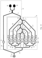
- FIG. 1 is a block diagram depicting a configuration of an N-bit optical DAC according to Embodiment 1 of the present invention.
- FIG. 2 is a graph depicting an input/output characteristic of the N-bit optical DAC according to Embodiment 1 of the present invention.
- FIG. 3 is a block diagram depicting a configuration of an N-bit optical DAC according to Embodiment 2 of the present invention.
- FIG. 4 is a graph depicting an input/output characteristic of the N-bit optical DAC according to Embodiment 2 of the present invention.
- FIG. 5 is a block diagram depicting a configuration of an N-bit optical DAC according to Embodiment 3 of the present invention.
- FIG. 6 is a graph depicting an input/output characteristic of the N-bit optical DAC according to Embodiment 3 of the present invention.
- FIG. 7 is a block diagram depicting a configuration of an N-bit optical DAC according to Embodiment 4 of the present invention.
- FIG. 8 is a perspective view depicting a configuration of a bias port-included Y coupling element in the N-bit optical DAC according to Embodiment 4 of the present invention.
- FIG. 9 is a plan view depicting the configuration of the bias port-included Y coupling element in the N-bit optical DAC according to Embodiment 4 of the present invention.
- FIG. 10 is a perspective view depicting another configuration of the bias port-included Y coupling element in the N-bit optical DAC according to Embodiment 4 of the present invention.
- FIG. 11 is a perspective view depicting another configuration of the bias port-included Y coupling element in the N-bit optical DAC according to Embodiment 4 of the present invention.
- FIG. 12 (A) to FIG. 12 (C) are graphs depicting the input/output characteristic of the N-bit optical DAC according to Embodiment 4 of the present invention.
- FIG. 13 is a block diagram depicting a configuration of an N-bit optical DAC according to Embodiment 5 of the present invention.
- FIG. 14 is a block diagram depicting a configuration of an N-bit optical DAC according to Embodiment 6 of the present invention.
- FIG. 15 is a graph depicting a relationship between a number of bits and a computing loss of the optical DAC.
- FIG. 16 (A) to FIG. 16 (D) are diagrams depicting concrete patterns of the configuration to actually operate the optical DAC in FIG. 14 .
- FIG. 17 is a block diagram depicting a configuration of a simulation target optical DAC according to Embodiment 6 of the present invention.
- FIG. 18 is a graph depicting a result of simulating the temporal change of the optical signal intensity of each bit in the configuration in FIG. 17 .
- FIG. 19 is a graph depicting a result of simulating the temporal change of the intensity of an optical signal detected by a photodetector in the configuration in FIG. 17 .
- FIG. 20 is a block diagram depicting a configuration of an N-bit optical DAC according to Embodiment 7 of the present invention.
- FIG. 21 is a block diagram depicting a configuration of the simulation target optical DAC according to Embodiment 7 of the present invention.
- FIG. 22 shows graphs depicting a result of simulating the temporal change of the absolute phase of the optical signal of each bit in the configuration in FIG. 21 .
- FIG. 23 is a graph depicting a result of simulating the temporal change of the intensity of the optical signal detected by a photodetector in the configuration in FIG. 21 .
- FIG. 24 is a graph depicting a result of simulating the temporal change of the absolute phase of the optical signal detected by a photodetector in the configuration in FIG. 21 .
- FIG. 25 is a graph depicting a result of simulating the temporal charge of the intensity of an electric signal output from a subtracter in the configuration of FIG. 21 .
- FIG. 27 is a block diagram depicting a configuration in the case of applying the phase modulation system to the N-bit optical DAC according to Embodiment 2 of the present invention.
- FIG. 28 is a block diagram depicting a configuration in the case of applying the phase modulation system to the N-bit optical DAC according to Embodiment 3 of the present invention.
- FIG. 29 is a block diagram depicting a configuration of an N-bit optical DAC according to Embodiment 8.
- FIG. 30 is a block diagram depicting another configuration of the N-bit optical DAC according to Embodiment 8.
- FIG. 31 is a diagram depicting an effect of inputting a bias light to a bias port of the Y coupling element.
- FIG. 32 is a block diagram depicting a configuration in a case of adding the Y coupling element in the final stage of the N-bit optical DAC according to Embodiments 1 and 5 of the present invention.
- FIG. 33 is a block diagram depicting a configuration in a case of adding the Y coupling element in the final stage of the N-bit optical DAC according to Embodiment 2 of the present invention.
- FIG. 34 is a block diagram depicting a configuration in a case of adding the Y coupling element in the final stage of the N-bit optical DAC according to Embodiment 3 of the present invention.
- FIG. 35 is a block diagram depicting a configuration in a case of adding the Y coupling element in the final stage of the N-bit optical DAC according to Embodiment 6 of the present invention.
- FIG. 1 is a block diagram depicting a configuration of an N-bit DAC, which is an optical computing unit according to Embodiment 1 of the present invention.
- the N-bit optical DAC is constituted of: cascade-connected N number of Y coupling elements 1 - 1 to 1 -N (N is 2 or greater integer) having two inputs and 1 output; an optical waveguide 2 - 1 that is connected to one optical input port of the Y coupling element 1 - 1 in the first stage; an optical waveguide 2 -M (M is an integer in a 2 to N range) that connects an optical output port of a Y coupling element 1 -(M ⁇ 1) in the (M ⁇ 1)th stage and one optical input port of a Y coupling element 1 -M in the Mth stage, so as to input the signal light output from the Y coupling element 1 -(M ⁇ 1) to the Y coupling element 1 -M; optical wave guides 3 - 1 to 3
- a dielectric optical wire such as a planar lightwave circuit (PLC) or a semiconductor optical wiring, such as an Si wire, can be used respectively.
- PLC planar lightwave circuit
- Si wire semiconductor optical wiring
- Continuous lights having the same wavelength and same intensity are input to the optical waveguides 3 - 1 to 3 -N respectively.
- a continuous laser light emitted from a continuous laser light source is equally divided into N by a 1:N splitter, and the divided light is input to each optical waveguide 3 - 1 to 3 -N respectively.
- the optical waveguide 2 - 1 corresponds to zero input. That is, light is not input to the optical waveguide 2 - 1 .
- the optical input to the optical waveguide 3 - 1 (i is an integer in a 1 to N range) corresponds to the input of the i-th bit (i is an integer in a 1 to N range).
- the optical input to the optical waveguide 3 - 1 corresponds to the least significant bit (LSB)
- the optical input to the optical waveguide 3 -N corresponds to the most significant bit (MSB).
- each optical intensity modulator 5 - 1 to 5 -N which is disposed for each bit of the N-bit electric digital signal, a variable optical attenuator (VOA) can be used.
- Each of the optical intensity modulators 5 - 1 to 5 -N interrupts the continuous light propagating each optical waveguide 3 - 1 to 3 -N respectively if the corresponding bit input of the electric digital signal is “0”, and allows the continuous light to pass if the bit input is “1”.
- the continuous light that propagates through each optical waveguide 3 - 1 to 3 -N is individually turned ON/OFF in accordance with the corresponding bit of the N-bit electric digital signal respectively. In this way, the signal light to be input to the other optical input port of each Y coupling element 1 - 1 to 1 -N is generated.
- the transmittance T of the light which was input from each of the two optical input ports of the Y coupling element 1 - i to the optical output port of the Y coupling element 1 - i , is 0.25 respectively.
- a fixed optical attenuator of which loss is 6 dB, may be disposed so that the light propagating through the optical waveguide 3 - 1 attenuates by 6 dB and is introduced to the optical waveguide 2 - 2 .
- the input and output of the optical intensity modulator 5 - 1 may be adjusted so that the relative intensity of the output light, with respect to the input light, becomes 0.25.
- phase shifter in each optical waveguide 3 - 1 to 3 -N respectively.
- this phase shifter are: a heater type phase shifter which controls the phase of the guided light by changing the refractive index of the optical waveguide by the thermo-optical effect; and a phase shifter that controls the phase of the guided light by changing the refractive index of the optical waveguide by the electro-optical effect.
- the final optical output (DAC output) of the N-bit optical DAC is acquired from the optical waveguide 4 .
- the abscissa in FIG. 2 indicates an electric digital signal; and the ordinate indicates the normalized value of the amplitude of the optical output of the N-bit optical DAC, and the amplitude values of the optical output of the N-bit optical DAC, with respect to all combinations of the electric digital signals (“00000000” to “11111111”), are plotted.
- the amplitude value of the optical output linearly increases as the digital input value increases, that is, the N-bit optical DAC is operating normally.
- the maximum optical output amplitude value in the case where all input bits are “1” is ((2 N -1)/2 N ) 1/2 to 1. Since the total value of the optical input is N, the loss L DAC caused by the computation of the optical DAC is 10 log 10 (N/(2 N ⁇ 1)2 N )) to 10 log 10 (N) [dB].
- FIG. 3 is a block diagram depicting a configuration of an N-bit optical DAC, which is an optical computing unit according to Embodiment 2 of the present invention.
- the N-bit optical DAC of Embodiment 2 is constituted of: a cascade-connected (N ⁇ 1) number of Y coupling/Y branching elements 10 - 1 to 10 -(N ⁇ 1) having two inputs and two outputs; a Y coupling element 13 of which one input is one optical output of the Y coupling/Y branching element 10 -(N ⁇ 1) in the final stage; an optical waveguide 14 - 1 that is connected to one optical input port of the Y coupling/Y branching element 10 - 1 in the first stage; an optical waveguide 14 - k (k is an integer in 2 to (N ⁇ 1) range) that connects one optical output port of the Y coupling/Y branching element 10 -( k ⁇ 1) in the (k ⁇ 1)th stage and one optical input port of the
- Each Y coupling/Y branch element 10 - 1 to 10 -(N ⁇ 1) is constituted of the Y coupling element 11 having two inputs and one output, and the Y branching element 12 of which input is the optical output of the Y coupling element 11 .
- the Y coupling element 11 of each Y coupling/Y branching element 10 - j (j is an integer in a 1 to (N ⁇ 1) range) couples the propagating lights in the optical waveguide 14 - j and the optical waveguide 15 - j at equal ratios, and outputs the coupled light.
- the transmittance T 11 of the light which was input to each of the two optical input ports of the Y coupling element 11 , propagated to the optical output port of the Y coupling element 11 is 0.5 respectively.
- each of the N number of optical intensity modulators 18 - 1 to 18 -N interrupts the continuous light propagating each optical waveguide 15 - 1 to 15 -N respectively if the bit input of the corresponding electric digital signal is “0”, and allows the continuous light to pass if the bit input is “1”. Thereby the signal light to be input to the other optical input port of each Y coupling/Y branching element 10 - 1 to 10 -(N ⁇ 1) and the Y coupling element 13 is generated.
- the final optical output (DAC output) of the N-bit optical DAC is acquired from the optical waveguide 17 .
- the N-bit optical DAC is operating normally.
- the maximum optical output amplitude value is ((2 N ⁇ 1)/2 N-1 ) 1/2 to ⁇ 2 in the case where all input bits are “1”.
- Embodiment 2 over the configuration of Embodiment 1, are as follows.
- the loss L DAC caused by the computation of the optical DAC is 3 dB.
- the maximum optical output amplitude value is up to ⁇ 2, as mentioned above, which means that the optical output is larger than Embodiment 1.
- the Y coupling/Y branching element of which T is up to 0.5 has lower reflectance, and is more easily designed than Embodiment 1.
- (C) DACs having a low number of bits can be simultaneously generated.
- 1 to (N ⁇ 1) bits of DAC output can be acquired from the optical waveguides 16 - 1 to 16 -(N ⁇ 1).
- the DAC output having a low number of bits can be used for a monitor port for operation calibration.
- a resolution switch function can be implemented.
- FIG. 5 is a block diagram depicting a configuration of an N-bit optical DAC, which is an optical computing unit according to Embodiment 3 of the present invention.
- the N-bit optical DAC of Embodiment 3 is constituted of: cascade-connected N number of Y coupling/Y branching elements 10 - 1 to 10 -N having two inputs and two outputs; an optical waveguide 14 - 1 connected to one optical input port of the Y coupling/Y branching element 10 - 1 in the first stage; an optical waveguide 14 -K (K is an integer in a 2 to N range) that connects one optical output port of the Y coupling/Y branching element 10 -(K ⁇ 1) in the (K ⁇ 1)th stage and one optical input port of the Y coupling/Y branching element 10 -K in the K-th stage; optical waveguides 15 - 1 to 15 -N that are connected to the other optical input ports of the Y coupling/Y branching elements 10
- the N-bit optical DAC of Embodiment 3 largely has the same configuration as Embodiment 2, and the method of inputting the continuous light is the same as Embodiment 2.
- a difference from Embodiment 2 is that a total number of Y coupling/Y branching elements is N, which is one more than Embodiment 2, using the Y coupling/Y branching element 10 -N instead of the Y coupling element 13 .
- the cascade-connected (N ⁇ 1) number of Y coupling elements 19 - 1 to 19 -(N ⁇ 1) are disposed, and the output of the Y coupling element 19 -(N ⁇ 1) in the final stage is the output of the bit counter (bit counter output). From this output of the bit counter, the light having an amplitude value, which is in proportion to a number of “1s” of the input digital signal, is output.
- the N-bit DAC computation and the N-bit counter computation can be executed simultaneously.
- OptiSystem which is an optical communications system simulator made by Optiwave Systems Inc.
- a bit rate of the signal generation is 10 Gbps
- DAC output amplitude values of the optical output of the N-bit optical DAC
- bit counter output bit counter output
- the abscissa in FIG. 6 indicates the time (ns).
- the electric signals are acquired by performing the photoelectric conversion on the optical output of the optical waveguide 4 using the photodetector 6 .
- the electric signals are acquired by performing photoelectric conversion on the optical outputs of the optical waveguides 16 - 1 to 16 -(N ⁇ 1) and 17 , using the photodetectors 23 - 1 to 23 -N respectively.
- the electric signals are acquired by performing photoelectric conversion on the output of the optical waveguide 17 using the photodetector 24 , and performing photoelectric conversion on the output of the optical waveguide 22 using the photodetector 25 .
- FIG. 7 is a block diagram depicting an N-bit optical DAC according to Embodiment 4, and a composing element the same as FIG. 1 is denoted with the same reference sign.
- the N-bit optical DAC of Embodiment 4 is constituted of: cascade-connected N number of bias port-included Y coupling elements 1 a - 1 to 1 a -N having three inputs and one output; an optical waveguide 2 - 1 that is connected to one optical input port of the bias port-included Y coupling element 1 a - 1 in the first stage; an optical waveguide 2 -M (M is an integer in a 2 to N range) that connects an optical output port of a bias port-included Y coupling element 1 a -(M ⁇ 1) in the (M ⁇ 1)th stage and one optical input port of a bias port-included Y coupling element 1 a -M in the M-th stage; optical waveguides 3 - 1 to 3
- FIG. 8 is a perspective view depicting the configuration of the bias port-included Y coupling element 1 a - 1
- FIG. 9 is a plan view depicting the configuration of the bias port-included Y coupling element 1 a - 1 .
- the bias port-included Y coupling element 1 a - 1 includes: a substrate 101 formed of a first dielectric material; and an optical waveguide 102 , an optical waveguide 103 , an optical waveguide 104 and an optical waveguide 105 (bias port) which are formed on one surface 101 a of the substrate 101 , and are formed of a second dielectric material having a higher refractive index than the first dielectric material.
- An example of the first dielectric material constituting the substrate 101 is silica (SiO 2 ) quartz.
- An example of the second dielectric material constituting the optical waveguides 102 to 105 is silicon (Si).
- the refractive index of silica is 1.4 in the communication wavelength band (e.g. 1.5 ⁇ m wavelength), while the refractive index of silicon (Si) is 3.5. Therefore, if the optical waveguides 102 to 105 are constituted of silicon, the substrate and air function as a clad that confines light inside the optical waveguides 102 to 105 .
- the bias port-included Y coupling element 1 a - 1 is configured on the planar optical waveguide.
- the optical waveguide 102 and the optical waveguide 103 which function as optical input ports, are disposed symmetrically with respect to the extended line of the optical waveguide 104 , which functions as an optical output port.
- the optical waveguide 105 is an optical waveguide for inputting the bias light, and functions as a bias port.
- the optical waveguide 105 which functions as the bias port, is disposed between the optical waveguide 102 and the optical waveguide 103 .
- the optical waveguide 105 is disposed on the extended line of the optical waveguide 104 .
- This tapered end of the optical waveguide 105 is referred to as the “tapered portion 105 a ”.
- This tapered portion 105 a is disposed close to the optical waveguide 102 and the optical waveguide 103 of the Y coupling element with spacing. As a result, the optical waveguide 102 , the optical waveguide 103 and the optical waveguide 105 optically couple with each other.
- the input signal lights propagate through the optical waveguides 102 and 103 , which function as the optical input ports, interfere with the bias light propagating through the optical waveguide 105 , and the output light is output from the optical waveguide 104 , which functions as the optical output port.
- the bias port-included Y coupling element 1 a - 1 can be manufactured in the following steps. That is, a silicon-on-insulator (SOI) substrate having a low loss monocrystal silicon layer is prepared, and after a photosensitive material coated on the surface of the monocrystal silicon layer is patterned into a predetermined pattern, as illustrated in FIG. 9 , for example, the silicon layer is etched. Thereby the element illustrated in FIG. 8 can be acquired.
- SOI silicon-on-insulator
- FIG. 10 is a perspective view depicting another configuration of the bias port-included Y coupling element 1 a - 1
- FIG. 11 is a plan view depicting another configuration of the bias port-included Y coupling element 1 a - 1 .
- this bias port-included Y coupling element 1 a - 1 includes: a substrate 201 formed of a first dielectric material, such as silica (SiO 2 ); and an optical waveguide 202 , an optical waveguide 203 , an optical waveguide 204 and an optical waveguide 205 which are formed of a second dielectric material having a higher refractive index than the first dielectric material.
- a first dielectric material such as silica (SiO 2 )
- an optical waveguide 202 , an optical waveguide 203 , an optical waveguide 204 and an optical waveguide 205 which are formed of a second dielectric material having a higher refractive index than the first dielectric material.
- the optical waveguide 202 and the optical waveguide 203 function as optical input ports
- the optical waveguide 204 functions as an optical output port
- the optical waveguide 205 functions as a bias port.
- the optical waveguide 205 which functions as a bias port, is disposed between the optical waveguide 202 and the optical waveguide 203 , which function as optical input ports.
- the optical waveguide 202 and the optical waveguide 203 are disposed symmetrically with respect to the optical waveguide 205 in the plan view.
- the optical waveguide 205 and the optical waveguide 204 which functions as an optical output port, are connected with each other at one end thereof.
- the optical waveguide 202 and the optical waveguide 203 which function as optical input ports, have coupling portions 202 a and 203 a , to couple with the optical waveguide 205 , which functions as the bias port respectively. That is, the coupling portions 202 a and 203 a are tip portions of the optical waveguide 202 and the optical waveguide 203 for the length L DC , which are disposed in parallel with spacing g DC with the optical waveguide 204 respectively.
- the optical waveguide 202 and the optical waveguide 203 have the coupling portions 202 a and 203 a respectively, the optical waveguide 202 , the optical waveguide 203 and the optical waveguide 205 , which are disposed apart from each other yet are close enough to make coupling possible, constitute a directional coupler.
- the length L DC of the coupling portions 202 a and 203 a is preferably about 90% of the 3 dB coupling length.
- bias port-included Y coupling element 1 a - 1 has been described, but the configuration of the other bias port-included Y coupling elements 1 a - 2 to 1 a -N are also the same as the configuration of the bias port-included Y coupling element 1 a - 1 .
- the bias light having the fixed intensity P bias is input from a continuous laser light source (not illustrated) to the bias ports of all the bias port-included Y coupling elements 1 a - 1 to 1 a -N.
- the phase of the signal light which is input to the two optical input ports of each bias port-included Y coupling element 1 a - 1 to 1 a -N and the phase of the bias light which is input to the bias port are assumed to be a same phase.
- the abscissa indicates an electric digital signal
- the ordinate indicates the normalized value of the optical output intensity of the N-bit optical DAC.
- FIG. 12 (A) indicates a case where the product T bias P bias of the transmittance T bias of the bias light and the intensity P bias of the bias light is 0,
- FIG. 12 (B) indicates a case where T bias P bias is 0.0625
- FIG. 12 (C) indicates a case where T bias P bias is 0.25.
- the characteristic indicated by the broken line 301 in FIG. 12 (A) to FIG. 12 (C) is a characteristic when the actual input/output characteristic indicated by the solid line 300 is linearly approximated.
- R 2 is a mean square error between the actual input/output characteristic and linear approximation thereof. In the example in FIG. 12 (A) to FIG. 12 (C) , the mean square errors R 2 are 0.9373, 0.9926 and 0.9973 respectively. In this way, as T bias P bias increases, the input/output relationship of the N-bit optical DAC becomes closer from a quadratic function to a linear function.
- the intensity P bias of the bias light is appropriately adjusted, the relationship between the input digital signal and the output of the photodetector 6 can be linear, and the electric circuit side need not perform square root processing on the output of the photodetector 6 .
- Embodiment 4 may be applied to Embodiments 2 and 3.
- the Y coupling element 11 of each Y coupling/Y branching element 10 - 1 to 10 -N and the Y coupling element 13 are replaced with a bias port-included Y coupling element respectively.
- FIG. 13 is a block diagram depicting an N-bit optical DAC, which is an optical computing unit according to Embodiment 5, and a composing element the same as FIG. 1 is denoted with the same reference sign.
- N 8
- the optical DAC coupling unit 30 corresponding to FIG. 1 and the coherent detection unit 31 are integrated.
- the continuous laser light emitted from a continuous laser light source 32 is divided equally into 2 by a Y branching element 33 .
- One side of the continuous light branched by the Y branching element 33 is input to a Y branching element 35 via an optical waveguide 34 .
- the Y branching element 35 divides the continuous light input from the optical waveguide 34 equally into 2.
- One side of the continuous light branched by the Y branching element 35 is input to a Y branching element 38 via an optical waveguide 36
- the other side of the branched continuous light is input to a Y branching element 39 via an optical waveguide 37 .
- the Y branching element 38 divides the continuous light input from the optical waveguide 36 equally into 2
- the Y branching element 39 divides the continuous light input from the optical waveguide 37 equally into 2.
- One side of the continuous light branched by the Y branching element 38 is input to a Y branching element 44 via an optical waveguide 40
- the other side of the branched continuous light is input to a Y branching element 45 via an optical waveguide 41 .
- One side of the continuous light branched by the Y branching element 39 is input to a Y branching element 46 via an optical waveguide 42
- the other side of the branched continuous light is input to a Y branching element 47 via an optical waveguide 43 .
- One side of the continuous light branched by the Y branching element 44 is input to an optical waveguide 3 - 8 , and the other side of the branched continuous light is input to an optical waveguide 3 - 5 .
- One side of the continuous light branched by the Y branching element 45 is input to an optical waveguide 3 - 4 , and the other side of the branched continuous light is input to an optical waveguide 3 - 1 .
- One side of the continuous light branched by the Y branching element 46 is input to an optical waveguide 3 - 2 , and the other side of the branched continuous light is input to an optical waveguide 3 - 3 .
- One side of the continuous light branched by the Y branching element 47 is input to an optical waveguide 3 - 6 , and the other side of the branched continuous light is input to an optical waveguide 3 - 7 .
- input of the continuous light to the optical waveguides 3 - 1 to 3 - 8 described in Embodiment 1, can be implemented.
- 48 - 1 to 48 - 8 in FIG. 13 indicates the phase shifters described in Embodiment 1.
- a coherent detection unit 31 is constituted of: an optical waveguide 50 connected to the other optical output port of the Y branching element 33 ; a phase shifter 51 disposed on the optical waveguide 50 ; a 3 dB coupler 52 (MMI coupler) which couples the propagated lights through an optical waveguide 4 and the optical waveguide 50 at equal ratios, divides the coupled light equally into 2, and outputs the divided lights; a photodetector 53 that converts one output light from the 3 dB coupler 52 into an electric signal; and a photodetector 54 that converts the other output light from the 3 dB coupler 52 into an electric signal.
- MMI coupler MMI coupler
- the phase shifter 51 is adjusted in advance, so that the phase difference between the output light, which propagates through the optical waveguide 4 from the optical DAC computing unit 30 and is input to the 3 dB coupler 52 , and the reference light which propagates through the optical waveguide 50 and is input to the 3 dB coupler 52 , becomes ⁇ /2.
- the two outputs from the 3 dB coupler 52 are received by the two different photodetectors 53 and 54 , and the difference between the two electric signals output from the photodetectors 53 and 54 is determined by a subtracter (not illustrated). In this way, the optical amplitude value can be detected using the configuration of a so called “balanced detector”.
- a coherent optical receiver normally synchronizes the phases of the locally emitted lights that are different from the light source of the signal light so as to generate a reference light. This phase synchronization requires high cost.
- the transmitter and receiver disposed close to each other are integrated, hence only the coherent detection unit 31 is required for the reference light, whereby the homodyne detection can be performed by the same continuous laser light source 32 of the optical DAC computing unit 30 .
- Embodiment 5 a case of applying the homodyne detection to Embodiment 1 was described, but the homodyne detection may be applied to Embodiments 2 to 4.
- the coherent detection unit is disposed instead of the photodetectors 23 - 1 to 23 -N respectively, so that the lights from the same continuous laser light sources of the optical waveguides 15 - 1 to 15 -N are input to one optical input port of the 3 dB coupler, and the lights from the optical waveguides 16 - 1 to 16 -(N ⁇ 1) and 17 are input to the other optical input port of the 3 dB coupler.
- the coherent detection unit is disposed instead of the photodetectors 24 and 25 respectively, so that the lights from the same continuous light sources of the optical waveguides 15 - 1 to 15 -N are input to one optical input port of the 3 dB coupler, and the lights from the optical waveguides 17 and 22 are input to the other optical input port of the 3 dB coupler.
- the coherent detection unit is disposed instead of the photodetector 6 , so that the lights from the same continuous light sources of the optical waveguides 3 - 1 to 3 -N are input to one optical input port of the 3 dB coupler, and the light from the optical waveguide 4 is input to the other optical input port of the 3 dB coupler.
- Embodiment 6 of the present invention will be described next.
- the transmittance T 11 of the light, which was input to the two optical input ports of the Y coupling element 11 constituting the Y coupling/Y branching element 10 - j (j is an integer in a 1 to (N ⁇ 1) range) to the optical output port of the Y coupling element 11 is 0.5 respectively
- the transmittance T 12 of the light, which was input to the optical input ports of the Y branching element 12 constituting the Y coupling/Y branching element 10 - j to the two optical ports of the Y branching element 12 is 0.5 respectively.
- the light intensity difference is provided to each of the N number of lights, so that the (N ⁇ 1) number of lights corresponding to each bit of the N-bit electric digital signal, not including LSB, has a light intensity that is 4 times (6 dB) that of the light intensity of the light corresponding to the adjacent lower bit respectively.
- the light intensity difference is provided to the N number of lights corresponding to the N-bit electric digital signal at the output side of the modulator, but in Embodiment 6, the light intensity difference is provided to the N number of lights not only at the output side, but also at the input side of the modulator.
- FIG. 14 is a block diagram depicting a configuration of an N-bit optical DAC, which is an optical computing unit according to Embodiment 6.
- the transmittance T of the light which was input to the optical input port of the Y branching element 61 - i , to the two optical output ports of the Y branching element 61 - i , is 0.5 respectively.
- each Y branching element 61 - i is cascade-connected so that each Y branching element, not including the Y branching element at the most upstream side which inputs a single continuous light is input, enables the light output from one optical output port, out of the two optical output ports of the Y branching element at the upstream side, to be the input.
- the continuous laser light from a single continuous laser light source (not illustrated) is branched into N number of continuous lights corresponding to each bit of the N-bit electric digital signal, and a light intensity difference can be provided to the N number of continuous lights, so that the light intensity of the (N ⁇ 1) number of continuous lights corresponding to each bit of the N-bit electric digital signal, not including LSB, is twice (3 dB) that of the continuous light corresponding to the adjacent lower bit respectively.
- the light corresponding to the i-th bit counted from MSB of the N-bit electric digital signal is output from the optical output port, to which the Y branching element in the subsequent stage is not connected, out of the two optical output ports of the i-th Y branching element 61 - i counted from the most upstream side.
- the optical input to the optical waveguide 63 - i corresponds to the input of the i-th bit counted from LSB.
- each one of the optical intensity modulators 64 - 1 to 64 -N which are disposed for each bit of the N-bit electric digital signal, interrupts the continuous light propagating in each optical waveguide 63 - 1 to 63 -N if the corresponding bit input of the electric digital signal is “0”, and allows the continuous light to pass if the bit input is “1”.
- the optical waveguide 66 - 1 corresponds to zero input. That is, light is not input to the optical waveguide 66 - 1 .
- the Y coupling element 65 - i couples the propagating light in the optical waveguide 66 - i and the propagating light in the optical waveguide 63 - i at equal ratios (coupling ratio 1:1), and outputs the coupled light.
- the transmittance T of the light which was input from each of the two optical input ports of the Y coupling element 65 - i to the optical output port of the Y coupling element 65 - i , is 0.5 respectively.
- each Y coupling element 65 - i is cascade-connected such that the signal light, of which intensity was modulated by the optical intensity modulator 64 - i , becomes one optical input, and each Y coupling element, not including the Y coupling element at the most upstream side, enables the light output from the optical output port of the Y coupling element at the upstream side to be the other optical input.
- the N number of signal lights, of which intensity was modulated by the optical intensity modulators 64 - 1 to 64 -N, are coupled into one, and the light intensity difference can be provided to the N number of signal lights, so that the light intensity of the (N ⁇ 1) number of signal lights corresponding to each bit, not including the LSB of the N-bit electric digital signal, is twice (3 dB) that of the continuous light corresponding to the adjacent lower bit respectively.
- phase shifters 68 - 1 to 68 -N have been adjusted in advance, so that the optical output intensity of each Y coupling element 65 - 1 to 65 -N becomes the maximum (phases of the lights coupled by each Y coupling element 65 - 1 to 65 -N becomes the same phase) when each optical intensity modulator 64 - 1 to 64 -N is in the passing state.
- the final optical output (output) of the N-bit optical DAC 60 is acquired from the optical waveguide 67 .
- the computing loss Loss in Embodiment 6 can be defined in the following formula.
- P out_max is the maximum optical output intensity in the case where all the inputs of the N-bit electric digital signal are “1”
- a out_max is the optical output amplitude, and is the square root of P out_max .
- T is the optical intensity transmittance of the Y coupling elements 65 - 1 to 65 -N (ideally 0.5).
- FIG. 15 indicates the relationship of the number of N bits and the computing loss Loss of the N-bit optical DAC, determined by substituting Formula (5) for Formula (1).
- 400 in FIG. 15 indicates the computing loss Loss of the N-bit optical DAC 60 of Embodiment 6, and 401 indicates the computing loss Loss of the N-bit optical DAC of Embodiments 2 and 3.
- the computing loss Loss simply increases with respect to the number of bits N, while in Embodiment 6, the computing loss Loss simply decreases with respect to the number of bits N, and approaches zero loss.
- the computing loss Loss decreases with respect to the number of N bits, hence a configuration suitable for high resolution can be implemented.
- FIG. 16 (A) to FIG. 16 (D) indicate concrete patterns of the configuration to actually operate the N-bit optical DAC 60 in FIG. 14 .
- FIG. 16 (A) is a case of directly extracting the optical output. In this case, the continuous laser light from the continuous laser light source 70 is input to the N-bit optical DAC 60 .
- FIG. 16 (B) is a case of directly detecting the optical output of the N-bit optical DAC 60 using a single photodetector 71 .
- an electric signal can be acquired by performing photoelectric conversion on the optical output of the N-bit optical DAC 60 using the photodetector 71 .
- FIG. 16 (C) is a case where the Y coupling element 74 couples continuous lights having a specific amplitude and phase, then the coupled light is directly detected using a single photodetector 75 .
- the continuous laser light from the continuous laser light source 70 is equally divided into 2 by the Y branching element 72 , and one side of the continuous light is input to the N-bit optical DAC 60 , and the other side of the continuous light is coupled with the output light of the N-bit optical DAC 60 using the Y coupling element 74 .
- the phase of the phase shifter 73 has been adjusted in advance, so that the optical output intensity of the Y coupling element 74 becomes the maximum.
- FIG. 16 (D) is a case of performing coherent detection.
- the continuous laser light from the continuous laser light source 70 is equally divided into 2 by the Y branching element 76 , and one side of the continuous light is input to the N-bit optical DAC 60 , and the other side of the continuous light is coupled with the output light of the N-bit optical DAC 60 using the 3 dB coupler (MMI coupler) 78 .
- the phase shifter 77 may be adjusted in advance so that the phase difference between the optical light to be input from the N-bit optical DAC 60 to the 3 dB coupler 78 and the other side of the continuous light (reference light) branched by the Y branching element 76 becomes ⁇ /2.
- the 3 dB coupler 78 couples the output light of the N-bit optical DAC 60 and the reference light of which phase was adjusted by the phase shifter 77 at equal ratios, equally divides the coupled light into 2, and outputs the two lights.
- the photodetectors 79 and 80 convert the two output lights of the 3 dB coupler 78 into electric signals respectively.
- the subtracter 81 determines the difference between the two electric signals output from the photodetectors 79 and 80 .
- FIG. 18 is a result of simulating the temporal change of the optical signal intensity of each bit in the configuration of FIG. 17 .
- the ordinate indicates the optical signal intensity of each bit
- the abscissa indicate time.
- there is a twice (3 dB) intensity difference between each bit before coupling is performed by the Y coupling elements 65 - 1 to 65 - 4 .
- FIG. 19 is a result of simulating the temporal change of the intensity P out of the optical signal detected by the photodetector 71 .
- P out gradually increases by sequentially inputting the electric digital signals “0000” to “1111” to the optical intensity modulators 64 - 1 to 64 - 4 .
- the electric digital signal is “1111”
- the P out is up to 879 ⁇ W
- the computing loss is up to 0.56 dB.
- This value of the optical signal intensity P out matches with the value acquired by Formula (5).
- a spike of the signal is generated between “0111” to “1000”. This spike is generated by signals which instantly overlap without intent since the rise time and fall time of the optical modulation signal are finite. This spike, however, can be removed by using an appropriate low-pass filter.
- Embodiment 7 of the present invention will be described next.
- Embodiment 7 is an example when an optical phase modulator is used instead of the optical intensity modulator in Embodiment 6.
- FIG. 20 is a block diagram depicting a configuration of an N-bit optical DAC, which is an optical computing unit according to Embodiment 7, and a composing element the same as FIG. 14 is denoted with the same reference sign.
- N 4 in Embodiment 7
- optical waveguides 62 - 1 to 62 -N 63 - 1 to 63 -N
- Y branching elements 65 - 1 to 65 -N disposed on the optical waveguides 63 - 1 to 63 -N.
- N optical modulators
- Each optical phase modulator 69 - 1 to 69 -N which is disposed for each bit of the N-bit electric digital signal, outputs the continuous light propagating through each optical waveguide 63 - 1 to 63 -N without changing the phase (in-phase) if the corresponding bit input of the electric digital signal is “0”, and outputs the continuous light propagating through each optical waveguide 63 - 1 to 63 -N shifting the phase by ⁇ (reverse-phase) if the corresponding bit input of the electric digital signal is “1”.
- in-phase (0) or reverse-phase ( ⁇ ) is individually assigned to the continuous light propagating through each optical waveguide 63 - 1 to 63 -N, in accordance with the corresponding bit of the N-bit electric digital signal.
- Embodiment 7 the phase shifter in the N-bit optical DAC 60 a is unnecessary, whereby a number of composing elements can be decreased.
- Embodiment 7 coherent detection is essential to determine the positive/negative of the amplitude of the signal.
- a concrete pattern of the configuration that can actually operate the N-bit optical DAC 60 a in FIG. 20 is the pattern in FIG. 16 (D) alone.
- Embodiment 7 The following is the result of simulating the configuration of Embodiment 7 using OptiSystem (made by Optiwave Systems, Inc.), just like Embodiment 6.
- OptiSystem made by Optiwave Systems, Inc.
- FIG. 21 The simulation conditions are the same as (I) to (IV) described above, except that the optical phase modulators 69 - 1 to 69 - 4 are used instead of the optical intensity modulators 64 - 1 to 64 - 4 .
- FIG. 22 is a result of simulating the temporal change of the absolute phase of the optical signal of each bit in the configuration of FIG. 21 .
- Embodiment 7 is a phase modulation system
- the phase difference between each bit (relative phase) is modulated to 0/ ⁇ .
- the absolute phase fluctuates without maintaining the initial phase, since the line width of the laser light is 10 MHz, but the relative phase between bits is maintained at either 0 or ⁇ , hence all bits share the same laser light.
- FIG. 23 is a result of simulating the temporal change of the intensity P out of the optical signal acquired when 100% light is coupled with the photodetector 82 disposed on the optical waveguide 67 in FIG. 21
- FIG. 24 is a result of simulating the temporal change of the absolute phase of the optical signal detected by the photodetector 82 .
- the intensity P out of the optical signal is symmetrical with respect to the boundary between the electric digital signals “0111” and “1000”, but the absolute phase is reversed at this boundary.
- FIG. 25 is a result of simulating the temporal change of the electric signal intensity output from the subtracter 81 in FIG. 21 .
- the positive/negative electric field amplitude of the optical signal is detected by the homodyne detection, and it is confirmed that output increases linearly with respect to the increase of the digital input.
- Embodiment 7 a case of applying the phase modulation system to Embodiment 6 was described, but the phase modulation system may be applied to Embodiments 1 to 5.
- FIG. 26 indicates a configuration in the case of applying the phase modulation system to Embodiments 1 and 5
- FIG. 27 indicates a configuration in the case of applying the phase modulation system to Embodiment 2
- FIG. 28 indicates a configuration in the case of applying the phase modulation system to Embodiment 3.
- coherent detection is essential in the phase modulation system, but in FIG. 26 to FIG. 28 , the configuration related to homodyne detection (coherent detection unit 31 and Y branching element 33 in FIG. 13 , and Y branching element 76 , phase shifter 77 , 3 dB coupler 78 , photodetectors 79 and 80 , and subtracter 81 in FIG. 16 (D) ) is omitted.
- Embodiment 4 all the Y coupling elements 1 - 1 to 1 -N in Embodiments 1 and 5 are replaced with the bias port-included Y coupling elements, and the Y coupling elements 11 and the Y coupling elements 13 of all the Y coupling/Y branching elements 10 - 1 to 10 -N in Embodiments 2 and 3 are replaced with the bias port-included Y coupling elements.
- all the Y coupling elements 65 - 1 to 65 -N in Embodiments 6 and 7 may be replaced with the bias port-included Y coupling elements.
- FIG. 29 indicates a configuration in the case where the Y coupling elements 65 - 1 to 65 -N in Embodiment 6 are replaced with the bias port-included Y coupling elements 65 a - 1 to 65 a -N
- FIG. 30 indicates a configuration in the case where the Y coupling elements 65 - 1 to 65 -N in Embodiment 7 are replaced with the bias port-included Y coupling elements 65 a - 1 to 65 a -N.
- the Y coupling elements 1 - 1 to 1 -N and the Y coupling elements 11 and the Y coupling elements 13 of the Y coupling/Y branching elements 10 - 1 to 10 -N may be replaced with the bias port-included Y coupling elements.
- FIG. 31 is a diagram depicting the relationship between the input digital signal and the intensity of an optical signal detected by the photodetector 82 of the optical DAC, where 310 indicates the operation region of the optical DAC in the case of not inputting the bias light, and 311 indicates the operation region of the optical DAC in the case of inputting the bias light.
- any one of the Y coupling elements disposed before the photodetector may be replaced with the bias port-included Y coupling element.
- any one of the Y coupling elements 1 - 1 to 1 -N in FIG. 1 , FIG. 13 of FIG. 26 may be replaced with the bias port-included Y coupling element, or either one of the Y coupling element 11 and the Y coupling element 13 of the Y coupling/Y branching elements 10 - 1 to 10 -N in FIG. 3 , FIG. 5 , FIG. 27 or FIG. 28 may be replaced with the bias port-included Y coupling element, or any one of the Y coupling elements 65 - 1 to 65 -N in FIG. 14 or FIG. 20 may be replaced with the bias port-included Y coupling element.
- FIG. 32 indicates a configuration in the case of adding the Y coupling element 83 in the final stage of the optical DAC in Embodiment 1 or 5
- FIG. 33 indicates a configuration in the case of adding the Y coupling element 83 in the final stage of the optical DAC in Embodiment 2
- FIG. 34 indicates a configuration in the case of adding the Y coupling element 83 in the final stage of the optical DAC in Embodiment 3
- FIG. 35 indicates a configuration in the case of adding the Y coupling element 83 in the final stage of the optical DAC in FIG. 6 .
- the optical intensity modulators 5 - 1 to 5 -N, 18 - 1 to 18 -N and 64 - 1 to 64 -N are replaced with the optical phase modulators.
- Embodiments of the present invention can be applied to a technique to convert an electric digital signal into an analog signal using an optical circuit, for example.
Landscapes
- Physics & Mathematics (AREA)
- General Physics & Mathematics (AREA)
- Optics & Photonics (AREA)
- Nonlinear Science (AREA)
- Engineering & Computer Science (AREA)
- Microelectronics & Electronic Packaging (AREA)
- Optical Modulation, Optical Deflection, Nonlinear Optics, Optical Demodulation, Optical Logic Elements (AREA)
- Optical Integrated Circuits (AREA)
Abstract
Description
-
- 1, 11, 13, 19, 65, 74, 83 Y coupling element
- 1 a, 65 a Bias port-included Y coupling element
- 2 to 4, 14 to 17, 20 to 22, 34, 36, 37, 40 to 43, 50, 62, 63, 66, 67, 102 to 105, 202 to 205 Optical waveguide
- 5, 18, 64 Optical intensity modulator
- 6, 23 to 25, 53, 54, 71, 75, 79, 80, 82 Photodetector
- 10 Y coupling/Y branching element
- 12, 33, 35, 38, 39, 44 to 47, 61, 72, 76 Y branching element
- 30 Optical DAC computing unit
- 31 Coherent detection unit
- 32, 70 Continuous laser light source
- 48-1 to 48-8, 51, 68, 73, 77 Phase shifter
- 52, 78 3 dB coupler
- 60, boa N-bit optical DAC
- 69 Optical phase modulator
- 81 Subtracter
- 101, 201 Substrate.
Claims (14)
Applications Claiming Priority (5)
| Application Number | Priority Date | Filing Date | Title |
|---|---|---|---|
| JP2018037282 | 2018-03-02 | ||
| JP2018-037282 | 2018-03-02 | ||
| JP2018-156024 | 2018-08-23 | ||
| JP2018156024A JP6871206B2 (en) | 2018-03-02 | 2018-08-23 | Optical calculator |
| PCT/JP2019/005021 WO2019167620A1 (en) | 2018-03-02 | 2019-02-13 | Optical arithmetic unit |
Publications (2)
| Publication Number | Publication Date |
|---|---|
| US20200408989A1 US20200408989A1 (en) | 2020-12-31 |
| US12038607B2 true US12038607B2 (en) | 2024-07-16 |
Family
ID=67946320
Family Applications (1)
| Application Number | Title | Priority Date | Filing Date |
|---|---|---|---|
| US16/976,866 Active 2041-08-02 US12038607B2 (en) | 2018-03-02 | 2019-02-13 | Optical arithmetic unit |
Country Status (2)
| Country | Link |
|---|---|
| US (1) | US12038607B2 (en) |
| JP (1) | JP6871206B2 (en) |
Families Citing this family (11)
| Publication number | Priority date | Publication date | Assignee | Title |
|---|---|---|---|---|
| JP7277830B2 (en) * | 2019-11-11 | 2023-05-19 | 日本電信電話株式会社 | Planar optical waveguide device |
| WO2021166173A1 (en) * | 2020-02-20 | 2021-08-26 | 日本電信電話株式会社 | Optical iq modulator |
| US20230093295A1 (en) * | 2020-02-20 | 2023-03-23 | Nippon Telegraph And Telephone Corporation | Optical IQ Modulator |
| US20240031032A1 (en) * | 2020-12-10 | 2024-01-25 | Lightspeedai Labs Private Limited | Systems and methods for enabling an optics based compute system associated with transmission and reception |
| RU2756462C1 (en) * | 2021-01-28 | 2021-09-30 | Ордена Трудового Красного Знамени федеральное государственное бюджетное образовательное учреждение высшего образования «Московский технический университет связи и информатики» (МТУСИ). | Optical analog-to-digital converter |
| US20240097783A1 (en) * | 2021-03-22 | 2024-03-21 | Axonal Networks Inc. | Communication methods, systems and devices |
| JP7679876B2 (en) * | 2021-04-28 | 2025-05-20 | 日本電信電話株式会社 | Analog-to-digital conversion method and analog-to-digital converter |
| EP4535078A1 (en) * | 2022-06-03 | 2025-04-09 | Nippon Telegraph And Telephone Corporation | Optical calculation device and optical calculation method |
| WO2024013910A1 (en) * | 2022-07-13 | 2024-01-18 | 富士通株式会社 | Optical circuit, quantum computing apparatus, and optical circuit manufacturing method |
| US12470301B2 (en) * | 2023-01-06 | 2025-11-11 | Qualcomm Incorporated | Local light biasing for silicon photomultiplier-based optical wireless communication |
| WO2024161448A1 (en) * | 2023-01-30 | 2024-08-08 | 日本電信電話株式会社 | Optical processing device, optical processing system and optical processing method |
Citations (4)
| Publication number | Priority date | Publication date | Assignee | Title |
|---|---|---|---|---|
| US5039988A (en) | 1988-11-25 | 1991-08-13 | Rockwell International Corporation | Optoelectronic digital to analog converter |
| US5157461A (en) * | 1990-06-14 | 1992-10-20 | Smiths Industries Aerospace & Defense Systems Inc. | Interface configuration for rate sensor apparatus |
| US20080018513A1 (en) | 2006-07-18 | 2008-01-24 | Frazier Gary A | Optical digital to analog converter |
| US8526771B2 (en) * | 2008-09-15 | 2013-09-03 | Hewlett-Packard Development Company, L.P. | In-plane optical wave guide with area based splitter |
Family Cites Families (5)
| Publication number | Priority date | Publication date | Assignee | Title |
|---|---|---|---|---|
| JPS56155928A (en) * | 1980-05-06 | 1981-12-02 | Mitsubishi Electric Corp | Optical da converter |
| US7061414B2 (en) * | 2004-02-03 | 2006-06-13 | Lucent Technologies Inc. | Optical digital-to-analog converter |
| US8009995B2 (en) * | 2006-01-12 | 2011-08-30 | The United States Of America As Represented By The Secretary Of The Navy | Method and apparatus for photonic digital-to-analog conversion |
| US7889107B2 (en) * | 2009-06-11 | 2011-02-15 | University Of Seoul Industry Cooperation Foundation | Digital-to-analog converter |
| CN102621768B (en) * | 2012-03-22 | 2014-02-12 | 中国科学院半导体研究所 | N-bit Optical Digital-to-Analog Converter Based on Microring Resonator |
-
2018
- 2018-08-23 JP JP2018156024A patent/JP6871206B2/en active Active
-
2019
- 2019-02-13 US US16/976,866 patent/US12038607B2/en active Active
Patent Citations (5)
| Publication number | Priority date | Publication date | Assignee | Title |
|---|---|---|---|---|
| US5039988A (en) | 1988-11-25 | 1991-08-13 | Rockwell International Corporation | Optoelectronic digital to analog converter |
| US5157461A (en) * | 1990-06-14 | 1992-10-20 | Smiths Industries Aerospace & Defense Systems Inc. | Interface configuration for rate sensor apparatus |
| US20080018513A1 (en) | 2006-07-18 | 2008-01-24 | Frazier Gary A | Optical digital to analog converter |
| JP2009544061A (en) | 2006-07-18 | 2009-12-10 | レイセオン カンパニー | Optical digital / analog converter |
| US8526771B2 (en) * | 2008-09-15 | 2013-09-03 | Hewlett-Packard Development Company, L.P. | In-plane optical wave guide with area based splitter |
Non-Patent Citations (3)
| Title |
|---|
| Kita, Shota, et al., "Proposal of Low Latency Optical Digital/Analog Converter," Summary of the 65 Spring Lecture of the Japan Society of Applied Physics, Mar. 17, 2018, 2 pages. |
| Kita, Shota, et al., "Proposal of Optical Digital/Analog Converters with Reduced Loss to Scale," The 79 Fall Scientific Lecture of the Japan Society of Applied Physics Previews, Sep. 18, 2018, 2 pages, Nagoya City, Aichi. |
| Yang, Lin, et al., "Demonstration of a 3-bit Digital-to-Analog Convertor Based on Silicon Microring Resonators," Optics Letters, 2014, vol. 39, No. 19, pp. 5736-5740. |
Also Published As
| Publication number | Publication date |
|---|---|
| JP2019152848A (en) | 2019-09-12 |
| US20200408989A1 (en) | 2020-12-31 |
| JP6871206B2 (en) | 2021-05-12 |
Similar Documents
| Publication | Publication Date | Title |
|---|---|---|
| US12038607B2 (en) | Optical arithmetic unit | |
| Kumari et al. | All-optical binary to gray code converter using non-linear material based MIM waveguide | |
| CN113541806A (en) | 16 frequency multiplication millimeter wave signal generation device and method based on parallel Mach-Zehnder modulator | |
| US9507238B2 (en) | Linearized Bragg grating assisted electro-optic modulator | |
| JP3415267B2 (en) | Design method and manufacturing method of optical signal processor | |
| US11880116B2 (en) | Optical digital/analog converter | |
| US20150280828A1 (en) | Optical transceiver | |
| Stopinski et al. | Integrated optical delay lines for time-division multiplexers | |
| US12339561B2 (en) | Mach-Zehnder type optical modulator, optical transceiver, and dispersion compensation method | |
| JP7097548B2 (en) | Optical digital-to-analog converter | |
| US12001115B2 (en) | Optical modulator and method of use | |
| Baba et al. | Photonic crystal slow light devices fabricated by CMOS-compatible process | |
| Idres et al. | Optical binary switched delay line based on low loss multimode waveguide | |
| WO2019167620A1 (en) | Optical arithmetic unit | |
| US20100046879A1 (en) | Optical Modulator | |
| Nejadriahi et al. | Integrated all-optical fast Fourier transform: Design and sensitivity analysis | |
| CN120752578A (en) | Optical coupling devices | |
| RU2119182C1 (en) | Optical analog-to-digital converter | |
| El-Fiky et al. | C-band and O-band silicon photonic based low-power variable optical attenuators | |
| Dev et al. | Energy-Efficient Forward-Biased PIN Silicon Mach–Zehnder Modulator With 50 μm Active Phase Shifter Length | |
| JP3319681B2 (en) | Optical transmission line simulator | |
| Leven et al. | High speed integrated InP photonic digital-to-analog converter | |
| Taylor et al. | Channel waveguide electrooptic devices for communications and information processing | |
| Ke et al. | Tunable optical true time delay line based on ring array | |
| Hu et al. | An integrated two-stage cascaded Mach-Zehnder device in GaAs |
Legal Events
| Date | Code | Title | Description |
|---|---|---|---|
| FEPP | Fee payment procedure |
Free format text: ENTITY STATUS SET TO UNDISCOUNTED (ORIGINAL EVENT CODE: BIG.); ENTITY STATUS OF PATENT OWNER: LARGE ENTITY |
|
| AS | Assignment |
Owner name: NIPPON TELEGRAPH AND TELEPHONE CORPORATION, JAPAN Free format text: ASSIGNMENT OF ASSIGNORS INTEREST;ASSIGNORS:NOTOMI, MASAYA;KITA, SHOTA;NOZAKI, KENGO;AND OTHERS;SIGNING DATES FROM 20200623 TO 20200630;REEL/FRAME:053807/0984 |
|
| STPP | Information on status: patent application and granting procedure in general |
Free format text: APPLICATION DISPATCHED FROM PREEXAM, NOT YET DOCKETED |
|
| STPP | Information on status: patent application and granting procedure in general |
Free format text: DOCKETED NEW CASE - READY FOR EXAMINATION |
|
| STPP | Information on status: patent application and granting procedure in general |
Free format text: NON FINAL ACTION MAILED |
|
| STPP | Information on status: patent application and granting procedure in general |
Free format text: RESPONSE TO NON-FINAL OFFICE ACTION ENTERED AND FORWARDED TO EXAMINER |
|
| STPP | Information on status: patent application and granting procedure in general |
Free format text: AWAITING TC RESP., ISSUE FEE NOT PAID |
|
| STPP | Information on status: patent application and granting procedure in general |
Free format text: NOTICE OF ALLOWANCE MAILED -- APPLICATION RECEIVED IN OFFICE OF PUBLICATIONS |
|
| STPP | Information on status: patent application and granting procedure in general |
Free format text: AWAITING TC RESP., ISSUE FEE NOT PAID |
|
| STPP | Information on status: patent application and granting procedure in general |
Free format text: PUBLICATIONS -- ISSUE FEE PAYMENT RECEIVED |
|
| STPP | Information on status: patent application and granting procedure in general |
Free format text: PUBLICATIONS -- ISSUE FEE PAYMENT VERIFIED |
|
| STCF | Information on status: patent grant |
Free format text: PATENTED CASE |