US12009334B2 - Insulating paste-based conductive device and manufacturing method thereof - Google Patents
Insulating paste-based conductive device and manufacturing method thereof Download PDFInfo
- Publication number
- US12009334B2 US12009334B2 US17/721,418 US202217721418A US12009334B2 US 12009334 B2 US12009334 B2 US 12009334B2 US 202217721418 A US202217721418 A US 202217721418A US 12009334 B2 US12009334 B2 US 12009334B2
- Authority
- US
- United States
- Prior art keywords
- electrode
- electrodes
- insulating paste
- substrate
- circuit board
- Prior art date
- Legal status (The legal status is an assumption and is not a legal conclusion. Google has not performed a legal analysis and makes no representation as to the accuracy of the status listed.)
- Active, expires
Links
Images


Classifications
-
- H—ELECTRICITY
- H10—SEMICONDUCTOR DEVICES; ELECTRIC SOLID-STATE DEVICES NOT OTHERWISE PROVIDED FOR
- H10W—GENERIC PACKAGES, INTERCONNECTIONS, CONNECTORS OR OTHER CONSTRUCTIONAL DETAILS OF DEVICES COVERED BY CLASS H10
- H10W20/00—Interconnections in chips, wafers or substrates
- H10W20/01—Manufacture or treatment
- H10W20/031—Manufacture or treatment of conductive parts of the interconnections
- H10W20/032—Manufacture or treatment of conductive parts of the interconnections of conductive barrier, adhesion or liner layers
- H10W20/038—Manufacture or treatment of conductive parts of the interconnections of conductive barrier, adhesion or liner layers covering conductive structures
-
- H—ELECTRICITY
- H10—SEMICONDUCTOR DEVICES; ELECTRIC SOLID-STATE DEVICES NOT OTHERWISE PROVIDED FOR
- H10H—INORGANIC LIGHT-EMITTING SEMICONDUCTOR DEVICES HAVING POTENTIAL BARRIERS
- H10H20/00—Individual inorganic light-emitting semiconductor devices having potential barriers, e.g. light-emitting diodes [LED]
- H10H20/80—Constructional details
- H10H20/85—Packages
- H10H20/857—Interconnections, e.g. lead-frames, bond wires or solder balls
-
- H—ELECTRICITY
- H05—ELECTRIC TECHNIQUES NOT OTHERWISE PROVIDED FOR
- H05K—PRINTED CIRCUITS; CASINGS OR CONSTRUCTIONAL DETAILS OF ELECTRIC APPARATUS; MANUFACTURE OF ASSEMBLAGES OF ELECTRICAL COMPONENTS
- H05K3/00—Apparatus or processes for manufacturing printed circuits
- H05K3/30—Assembling printed circuits with electric components, e.g. with resistors
- H05K3/32—Assembling printed circuits with electric components, e.g. with resistors electrically connecting electric components or wires to printed circuits
- H05K3/321—Assembling printed circuits with electric components, e.g. with resistors electrically connecting electric components or wires to printed circuits by conductive adhesives
-
- H01L24/32—
-
- H—ELECTRICITY
- H05—ELECTRIC TECHNIQUES NOT OTHERWISE PROVIDED FOR
- H05K—PRINTED CIRCUITS; CASINGS OR CONSTRUCTIONAL DETAILS OF ELECTRIC APPARATUS; MANUFACTURE OF ASSEMBLAGES OF ELECTRICAL COMPONENTS
- H05K3/00—Apparatus or processes for manufacturing printed circuits
- H05K3/36—Assembling printed circuits with other printed circuits
- H05K3/368—Assembling printed circuits with other printed circuits parallel to each other
-
- H01L24/29—
-
- H01L24/83—
-
- H—ELECTRICITY
- H05—ELECTRIC TECHNIQUES NOT OTHERWISE PROVIDED FOR
- H05K—PRINTED CIRCUITS; CASINGS OR CONSTRUCTIONAL DETAILS OF ELECTRIC APPARATUS; MANUFACTURE OF ASSEMBLAGES OF ELECTRICAL COMPONENTS
- H05K1/00—Printed circuits
- H05K1/02—Details
- H05K1/14—Structural association of two or more printed circuits
- H05K1/144—Stacked arrangements of planar printed circuit boards
-
- H—ELECTRICITY
- H10—SEMICONDUCTOR DEVICES; ELECTRIC SOLID-STATE DEVICES NOT OTHERWISE PROVIDED FOR
- H10H—INORGANIC LIGHT-EMITTING SEMICONDUCTOR DEVICES HAVING POTENTIAL BARRIERS
- H10H20/00—Individual inorganic light-emitting semiconductor devices having potential barriers, e.g. light-emitting diodes [LED]
- H10H20/80—Constructional details
- H10H20/83—Electrodes
- H10H20/832—Electrodes characterised by their material
- H10H20/833—Transparent materials
-
- H—ELECTRICITY
- H10—SEMICONDUCTOR DEVICES; ELECTRIC SOLID-STATE DEVICES NOT OTHERWISE PROVIDED FOR
- H10W—GENERIC PACKAGES, INTERCONNECTIONS, CONNECTORS OR OTHER CONSTRUCTIONAL DETAILS OF DEVICES COVERED BY CLASS H10
- H10W20/00—Interconnections in chips, wafers or substrates
- H10W20/01—Manufacture or treatment
- H10W20/031—Manufacture or treatment of conductive parts of the interconnections
- H10W20/032—Manufacture or treatment of conductive parts of the interconnections of conductive barrier, adhesion or liner layers
- H10W20/052—Manufacture or treatment of conductive parts of the interconnections of conductive barrier, adhesion or liner layers by treatments not introducing additional elements therein
- H10W20/0526—Manufacture or treatment of conductive parts of the interconnections of conductive barrier, adhesion or liner layers by treatments not introducing additional elements therein by thermal treatment thereof
-
- H—ELECTRICITY
- H10—SEMICONDUCTOR DEVICES; ELECTRIC SOLID-STATE DEVICES NOT OTHERWISE PROVIDED FOR
- H10W—GENERIC PACKAGES, INTERCONNECTIONS, CONNECTORS OR OTHER CONSTRUCTIONAL DETAILS OF DEVICES COVERED BY CLASS H10
- H10W72/00—Interconnections or connectors in packages
- H10W72/30—Die-attach connectors
-
- H—ELECTRICITY
- H10—SEMICONDUCTOR DEVICES; ELECTRIC SOLID-STATE DEVICES NOT OTHERWISE PROVIDED FOR
- H10W—GENERIC PACKAGES, INTERCONNECTIONS, CONNECTORS OR OTHER CONSTRUCTIONAL DETAILS OF DEVICES COVERED BY CLASS H10
- H10W72/00—Interconnections or connectors in packages
- H10W72/90—Bond pads, in general
-
- H01L2224/05624—
-
- H01L2224/05639—
-
- H01L2224/05644—
-
- H01L2224/05647—
-
- H01L2224/05686—
-
- H01L2224/05693—
-
- H01L2224/2919—
-
- H01L2224/32145—
-
- H01L2224/32227—
-
- H01L2224/83201—
-
- H01L2224/83862—
-
- H01L24/05—
-
- H01L2924/0549—
-
- H01L2924/12041—
-
- H—ELECTRICITY
- H10—SEMICONDUCTOR DEVICES; ELECTRIC SOLID-STATE DEVICES NOT OTHERWISE PROVIDED FOR
- H10H—INORGANIC LIGHT-EMITTING SEMICONDUCTOR DEVICES HAVING POTENTIAL BARRIERS
- H10H20/00—Individual inorganic light-emitting semiconductor devices having potential barriers, e.g. light-emitting diodes [LED]
- H10H20/01—Manufacture or treatment
- H10H20/036—Manufacture or treatment of packages
- H10H20/0364—Manufacture or treatment of packages of interconnections
-
- H—ELECTRICITY
- H10—SEMICONDUCTOR DEVICES; ELECTRIC SOLID-STATE DEVICES NOT OTHERWISE PROVIDED FOR
- H10W—GENERIC PACKAGES, INTERCONNECTIONS, CONNECTORS OR OTHER CONSTRUCTIONAL DETAILS OF DEVICES COVERED BY CLASS H10
- H10W72/00—Interconnections or connectors in packages
- H10W72/071—Connecting or disconnecting
- H10W72/073—Connecting or disconnecting of die-attach connectors
- H10W72/07331—Connecting techniques
- H10W72/07332—Compression bonding, e.g. thermocompression bonding
-
- H—ELECTRICITY
- H10—SEMICONDUCTOR DEVICES; ELECTRIC SOLID-STATE DEVICES NOT OTHERWISE PROVIDED FOR
- H10W—GENERIC PACKAGES, INTERCONNECTIONS, CONNECTORS OR OTHER CONSTRUCTIONAL DETAILS OF DEVICES COVERED BY CLASS H10
- H10W72/00—Interconnections or connectors in packages
- H10W72/071—Connecting or disconnecting
- H10W72/073—Connecting or disconnecting of die-attach connectors
- H10W72/07331—Connecting techniques
- H10W72/07337—Connecting techniques using a polymer adhesive, e.g. an adhesive based on silicone or epoxy
- H10W72/07338—Connecting techniques using a polymer adhesive, e.g. an adhesive based on silicone or epoxy hardening the adhesive by curing, e.g. thermosetting
-
- H—ELECTRICITY
- H10—SEMICONDUCTOR DEVICES; ELECTRIC SOLID-STATE DEVICES NOT OTHERWISE PROVIDED FOR
- H10W—GENERIC PACKAGES, INTERCONNECTIONS, CONNECTORS OR OTHER CONSTRUCTIONAL DETAILS OF DEVICES COVERED BY CLASS H10
- H10W72/00—Interconnections or connectors in packages
- H10W72/30—Die-attach connectors
- H10W72/351—Materials of die-attach connectors
- H10W72/353—Materials of die-attach connectors not comprising solid metals or solid metalloids, e.g. ceramics
- H10W72/354—Materials of die-attach connectors not comprising solid metals or solid metalloids, e.g. ceramics comprising polymers
-
- H—ELECTRICITY
- H10—SEMICONDUCTOR DEVICES; ELECTRIC SOLID-STATE DEVICES NOT OTHERWISE PROVIDED FOR
- H10W—GENERIC PACKAGES, INTERCONNECTIONS, CONNECTORS OR OTHER CONSTRUCTIONAL DETAILS OF DEVICES COVERED BY CLASS H10
- H10W72/00—Interconnections or connectors in packages
- H10W72/90—Bond pads, in general
- H10W72/951—Materials of bond pads
- H10W72/952—Materials of bond pads comprising metals or metalloids, e.g. PbSn, Ag or Cu
-
- H—ELECTRICITY
- H10—SEMICONDUCTOR DEVICES; ELECTRIC SOLID-STATE DEVICES NOT OTHERWISE PROVIDED FOR
- H10W—GENERIC PACKAGES, INTERCONNECTIONS, CONNECTORS OR OTHER CONSTRUCTIONAL DETAILS OF DEVICES COVERED BY CLASS H10
- H10W72/00—Interconnections or connectors in packages
- H10W72/90—Bond pads, in general
- H10W72/951—Materials of bond pads
- H10W72/953—Materials of bond pads not comprising solid metals or solid metalloids, e.g. polymers, ceramics or liquids
-
- H—ELECTRICITY
- H10—SEMICONDUCTOR DEVICES; ELECTRIC SOLID-STATE DEVICES NOT OTHERWISE PROVIDED FOR
- H10W—GENERIC PACKAGES, INTERCONNECTIONS, CONNECTORS OR OTHER CONSTRUCTIONAL DETAILS OF DEVICES COVERED BY CLASS H10
- H10W90/00—Package configurations
- H10W90/701—Package configurations characterised by the relative positions of pads or connectors relative to package parts
- H10W90/731—Package configurations characterised by the relative positions of pads or connectors relative to package parts of die-attach connectors
- H10W90/732—Package configurations characterised by the relative positions of pads or connectors relative to package parts of die-attach connectors between stacked chips
-
- H—ELECTRICITY
- H10—SEMICONDUCTOR DEVICES; ELECTRIC SOLID-STATE DEVICES NOT OTHERWISE PROVIDED FOR
- H10W—GENERIC PACKAGES, INTERCONNECTIONS, CONNECTORS OR OTHER CONSTRUCTIONAL DETAILS OF DEVICES COVERED BY CLASS H10
- H10W90/00—Package configurations
- H10W90/701—Package configurations characterised by the relative positions of pads or connectors relative to package parts
- H10W90/731—Package configurations characterised by the relative positions of pads or connectors relative to package parts of die-attach connectors
- H10W90/734—Package configurations characterised by the relative positions of pads or connectors relative to package parts of die-attach connectors between a chip and a stacked insulating package substrate, interposer or RDL
Definitions
- the present invention relates to the field of basic conductive technologies of quantum technologies of electronic technologies, and more particularly, to an insulating paste-based conductive device and a manufacturing method thereof.
- the present invention aims to provide an insulating paste-based conductive device with integrated electric conduction, light conduction and heat conduction performances and a manufacturing method thereof.
- the present invention provides an insulating paste-based conductive device, which comprises a first substrate and a second substrate arranged relative to the first substrate, and further comprises at least one first electrode disposed below the first substrate, a second electrode disposed on the second substrate and corresponding to the first electrode, and an insulating paste coating disposed on a contact surface between the first electrode and the second electrode, wherein the insulating paste coating is electrically connected with the first electrode and the corresponding second electrode.
- a plurality of first electrodes arranged in an array are provided, a plurality of second electrodes arranged in an array are provided, the insulating paste coating disposed between the first electrode and the second electrode corresponding to the first electrode is linear, and the insulating paste coating disposed between the first substrate and the second substrate, and disposed between the adjacent first electrodes and the adjacent second electrodes is annular.
- the insulating paste coating is a thermosetting adhesive.
- the insulating paste coating has a nanometer thickness.
- the first electrode and the second electrode are non-transparent electrodes, specifically comprising copper electrodes, gold electrodes, silver electrodes, alloy electrodes, silver-burned electrodes, elargol electrodes or carbon electrodes.
- the first electrode and the second electrode are transparent electrodes, specifically comprising nano-silver electrodes, nano-aluminum electrodes, nano-copper electrodes or ITO electrodes.
- the present invention further provides a manufacturing method of the insulating paste-based conductive device, which comprises the following steps of:
- S 1 sizing a lower surface of the first electrode and/or an upper surface of the second electrode
- a method of sizing in step S 1 is adhesive spraying or adhesive dispensing.
- the curing in step S 3 is carried out at a heating temperature of 100° C. to 170° C., and the heating lasts for 60 minutes to 90 minutes.
- step S 3 a curing pressure is applied to the upper surface of the first substrate and/or the lower surface of the second substrate.
- the present invention has good universality, such that the requirements of implementing or applying the art on a ceramic circuit board, a metal-based circuit board, an epoxy glass fiber circuit board, a flexible printed circuit board, a glass circuit board and a transparent circuit board can be set, and an electronic circuit board without a packaging element on the circuit boards above can also be manufactured.
- FIG. 1 is a schematic structural diagram of an insulating paste-based conductive device according to an embodiment of the present invention
- FIG. 2 is a schematic structural diagram of applying an adhering pressure on the insulating paste-based conductive device according to the embodiment of the present invention
- FIG. 3 is a schematic structural diagram of applying a curing pressure on the insulating paste-based conductive device according to the embodiment of the present invention
- FIG. 4 is a schematic structural diagram of protecting electrodes and areas thereof with an insulating paste of the insulating paste-based conductive device according to the embodiment of the present invention
- FIG. 5 is another schematic structural diagram of applying the curing pressure on the insulating paste-based conductive device according to the embodiment of the present invention.
- FIG. 6 is another schematic structural diagram of protecting the electrodes and the areas thereof with the insulating paste of the insulating paste-based conductive device according to the embodiment of the present invention.
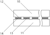
- an insulating paste-based conductive device comprises a first substrate 10 , a second substrate 11 arranged relative to the first substrate 10 , a plurality of first electrodes 12 disposed below the first substrate 10 and arranged in an array, a plurality of second electrodes 13 disposed on the second substrate 11 and arranged in an array, and an insulating paste coating 14 disposed on a contact surface between the first electrode 12 and the second electrode 13 .
- the insulating paste coating 14 is electrically connected with the first electrode 12 and the corresponding second electrode 13 .
- first electrode and one second electrode there may also be only one first electrode and one second electrode, and the first electrode and the second electrode are respectively laid on the first substrate 10 and the second substrate 11 by whole surfaces, so as to be suitable for some special occasions.
- the insulating paste coating 14 is a thermosetting adhesive, which may be a phenolic resin, an amino resin and an epoxy resin.
- the insulating paste coating 14 has a nanometer thickness.
- the first electrode 12 and the second electrode 13 are metal or nonmetal conductive electrodes. According to a light transmission performance, the first electrode 12 and the second electrode 13 may be divided into transparent and non-transparent electrodes. Taking the classification by the light transmission performance as an example, the non-transparent electrodes comprise copper electrodes, gold electrodes, silver electrodes, alloy electrodes, silver-burned electrodes, elargol electrodes and carbon electrodes (the electrodes are the nonmetal electrodes).
- the transparent electrodes comprise nano-silver electrodes, nano-aluminum electrodes, nano-copper electrodes and ITO electrodes (the electrodes are the metal electrodes).
- the lower surface of the first electrode 12 and/or the upper surface of the second electrode 13 are rough or non-rough surfaces, which is beneficial for electric conduction between the first electrode 12 and the second electrode 13 .
- the lower surface of the first electrode 12 and/or the upper surface of the second electrode 13 is sized (a method of sizing is adhesive spraying or adhesive dispensing), the first substrate 10 and/or the second substrate 11 is applied with an adhering pressure, so that the first electrode 12 and the second electrode 13 are electrically adhered, and then the first substrate 10 and the second substrate 11 are heated and cured to form the insulating paste coating 14 on the contact surface between the first electrode 12 and the second electrode 13 .
- the insulating paste coating 14 has the thickness of nanoscale.
- the insulating paste coating 14 does not contain any conductive medium.
- the insulating paste coating 14 disposed between the first electrode 12 and the second electrode 13 corresponding to the first electrode 12 is linear, and the insulating paste coating 14 disposed between the first substrate 10 and the second substrate 11 , and disposed between the adjacent first electrodes 12 and the adjacent second electrodes 13 is annular.
- the so-called “annular” is only a protective measure to protect electrode and non-electrode parts from oxidation, corrosion and damping with the insulating paste.
- the insulating paste coating disposed between the first electrode and the second electrode corresponding to the first electrode is linear.
- the present invention further provides a manufacturing method of the insulating paste-based conductive device, which comprises the following steps of:
- S 1 as shown in FIG. 1 , sizing a lower surface of the first electrode 12 and/or an upper surface of the second electrode 13 (a method of sizing is adhesive spraying or adhesive dispensing);
- a method of curing is heating the first substrate 10 and the second substrate 11 in an oven for curing at a heating temperature of 100° C. to 170° C., and the heating lasts for 60 minutes to 90 minutes.
- step S 3 a curing pressure is applied to the upper surface of the first substrate 10 and/or the lower surface of the second substrate 11 , so as to improve a conductivity between multiple pairs of electrodes.
- FIG. 5 is another schematic structural diagram of applying the curing pressure on the insulating paste-based conductive device according to the embodiment of the present invention, wherein the curing pressure is simultaneously applied to the upper surface of the first substrate 10 and the lower surface of the second substrate 11 .
- FIG. 6 is another schematic structural diagram of protecting the electrodes and the areas thereof with the insulating paste of the insulating paste-based conductive device according to the embodiment of the present invention, which is an effect diagram after only the second substrate 11 is subjected to adhesive dispensing or adhesive spraying.
- a principle of the present invention refers to a tunneling effect.
- the insulating paste coating of the present invention can protect the electrodes from oxidation, damping and corrosion.
- conductive adhesive connection of insulating paste may be carried out on a non-rough electrode surface.
- the present invention may be used in anti-electromagnetic interference, small-pitch LED screens, micron LED chips, semiconductor technologies, bioelectronics, light therapy and mobile phones.
- the insulating paste coating conductive technology of the present invention has integrated electric conduction, light conduction and heat conduction performances, and may be used in metamaterials, aerospace, radars, solar power generation and optical quantum communication.
- the present invention has a good universality, can meet the requirements of implementing or applying the art on a ceramic circuit board, a metal-based circuit board, an epoxy glass fiber circuit board, a flexible printed circuit board, a glass circuit board and a transparent circuit board, and can also manufacture an electronic circuit board without a packaging element on the circuit boards above.
Landscapes
- Engineering & Computer Science (AREA)
- Microelectronics & Electronic Packaging (AREA)
- Manufacturing & Machinery (AREA)
- Adhesives Or Adhesive Processes (AREA)
- Manufacturing Of Printed Wiring (AREA)
- Electroluminescent Light Sources (AREA)
- Devices For Indicating Variable Information By Combining Individual Elements (AREA)
- Non-Metallic Protective Coatings For Printed Circuits (AREA)
Abstract
Description
Claims (5)
Applications Claiming Priority (2)
| Application Number | Priority Date | Filing Date | Title |
|---|---|---|---|
| CN202210297900.1 | 2022-03-24 | ||
| CN202210297900.1A CN117276452A (en) | 2022-03-24 | 2022-03-24 | An insulating glue basic conductive device and its manufacturing method |
Publications (2)
| Publication Number | Publication Date |
|---|---|
| US20230307408A1 US20230307408A1 (en) | 2023-09-28 |
| US12009334B2 true US12009334B2 (en) | 2024-06-11 |
Family
ID=81851983
Family Applications (1)
| Application Number | Title | Priority Date | Filing Date |
|---|---|---|---|
| US17/721,418 Active 2042-11-11 US12009334B2 (en) | 2022-03-24 | 2022-04-15 | Insulating paste-based conductive device and manufacturing method thereof |
Country Status (3)
| Country | Link |
|---|---|
| US (1) | US12009334B2 (en) |
| CN (1) | CN117276452A (en) |
| GB (1) | GB2616920A (en) |
Citations (6)
| Publication number | Priority date | Publication date | Assignee | Title |
|---|---|---|---|---|
| US20120205816A1 (en) * | 2011-02-11 | 2012-08-16 | Hynix Semiconductor Inc. | Semiconductor chip and fabricating method thereof |
| US20140144677A1 (en) * | 2012-11-23 | 2014-05-29 | Subtron Technology Co., Ltd. | Package carrier |
| CN204045356U (en) | 2014-07-15 | 2014-12-24 | 高技企业股份有限公司 | an inductive device |
| CN110336576A (en) | 2019-06-26 | 2019-10-15 | 维沃移动通信有限公司 | Conductive devices and terminal equipment |
| CN110875202A (en) * | 2018-09-04 | 2020-03-10 | 中芯集成电路(宁波)有限公司 | Wafer-level packaging method and packaging structure |
| US20200105696A1 (en) * | 2018-09-28 | 2020-04-02 | Taiwan Semiconductor Manufacturing Company, Ltd. | Metal Bumps and Method Forming Same |
Family Cites Families (2)
| Publication number | Priority date | Publication date | Assignee | Title |
|---|---|---|---|---|
| CN104993041B (en) * | 2015-06-04 | 2019-06-11 | 陈建伟 | A kind of LED flip chip solid crystal conductive bonding structure and installation method thereof |
| JP2020107711A (en) * | 2018-12-27 | 2020-07-09 | 日東電工株式会社 | Semiconductor device manufacturing method |
-
2022
- 2022-03-24 CN CN202210297900.1A patent/CN117276452A/en active Pending
- 2022-04-15 US US17/721,418 patent/US12009334B2/en active Active
- 2022-04-21 GB GB2205843.2A patent/GB2616920A/en active Pending
Patent Citations (7)
| Publication number | Priority date | Publication date | Assignee | Title |
|---|---|---|---|---|
| US20120205816A1 (en) * | 2011-02-11 | 2012-08-16 | Hynix Semiconductor Inc. | Semiconductor chip and fabricating method thereof |
| US20140144677A1 (en) * | 2012-11-23 | 2014-05-29 | Subtron Technology Co., Ltd. | Package carrier |
| CN204045356U (en) | 2014-07-15 | 2014-12-24 | 高技企业股份有限公司 | an inductive device |
| CN110875202A (en) * | 2018-09-04 | 2020-03-10 | 中芯集成电路(宁波)有限公司 | Wafer-level packaging method and packaging structure |
| CN110875202B (en) * | 2018-09-04 | 2021-11-09 | 中芯集成电路(宁波)有限公司 | Wafer level packaging method and packaging structure |
| US20200105696A1 (en) * | 2018-09-28 | 2020-04-02 | Taiwan Semiconductor Manufacturing Company, Ltd. | Metal Bumps and Method Forming Same |
| CN110336576A (en) | 2019-06-26 | 2019-10-15 | 维沃移动通信有限公司 | Conductive devices and terminal equipment |
Also Published As
| Publication number | Publication date |
|---|---|
| GB202205843D0 (en) | 2022-06-08 |
| GB2616920A (en) | 2023-09-27 |
| US20230307408A1 (en) | 2023-09-28 |
| CN117276452A (en) | 2023-12-22 |
Similar Documents
| Publication | Publication Date | Title |
|---|---|---|
| US20180019385A1 (en) | Led flip chip die-bond conductive adhesive structure and mounting method thereof | |
| CN101502189B (en) | 3d electronic circuit device | |
| KR19990014197A (en) | Flip chip connection method, flip chip connection structure and electronic device using same | |
| TW201433766A (en) | Heat receiver for high power solar concentrator and method of assembling same | |
| US10811332B2 (en) | Thermal-dissipating substrate structure | |
| CN102891116B (en) | Embedded component packaging structure and manufacturing method | |
| WO2011148840A1 (en) | Solar cell module and method for manufacturing same | |
| US20190035961A1 (en) | High-conductivity and high-voltage solar photovoltaic glass panel | |
| US11665859B2 (en) | Heat dissipation conductive flexible board | |
| US7309838B2 (en) | Multi-layered circuit board assembly with improved thermal dissipation | |
| US20130140664A1 (en) | Flip chip packaging structure | |
| US12009334B2 (en) | Insulating paste-based conductive device and manufacturing method thereof | |
| TWI620337B (en) | Solar cell module manufacturing method | |
| CN203481215U (en) | Chip-type electronic part | |
| CN216980608U (en) | Insulating gum foundation conductive device | |
| CN209882211U (en) | HDI high density lamination circuit board | |
| WO2011148838A1 (en) | Photovoltaic cell module and photovoltaic cell | |
| CN102456684B (en) | Power transfer module | |
| CN114867206A (en) | Electronic structure and manufacturing method thereof | |
| CN108807352A (en) | A kind of New LED filament manufacturing technology | |
| CN222394805U (en) | Embedded semiconductor packaging structure | |
| US20260026344A1 (en) | Integrated circuit package | |
| JP2932772B2 (en) | Hybrid integrated circuit device | |
| CN111584367B (en) | Method for manufacturing semiconductor packaging glass by thick film circuit printing | |
| US20250285927A1 (en) | Method of manufacturing electronic components |
Legal Events
| Date | Code | Title | Description |
|---|---|---|---|
| FEPP | Fee payment procedure |
Free format text: ENTITY STATUS SET TO UNDISCOUNTED (ORIGINAL EVENT CODE: BIG.); ENTITY STATUS OF PATENT OWNER: SMALL ENTITY |
|
| FEPP | Fee payment procedure |
Free format text: ENTITY STATUS SET TO SMALL (ORIGINAL EVENT CODE: SMAL); ENTITY STATUS OF PATENT OWNER: SMALL ENTITY |
|
| STPP | Information on status: patent application and granting procedure in general |
Free format text: DOCKETED NEW CASE - READY FOR EXAMINATION |
|
| STPP | Information on status: patent application and granting procedure in general |
Free format text: NON FINAL ACTION MAILED |
|
| STPP | Information on status: patent application and granting procedure in general |
Free format text: RESPONSE TO NON-FINAL OFFICE ACTION ENTERED AND FORWARDED TO EXAMINER |
|
| STPP | Information on status: patent application and granting procedure in general |
Free format text: NOTICE OF ALLOWANCE MAILED -- APPLICATION RECEIVED IN OFFICE OF PUBLICATIONS |
|
| AS | Assignment |
Owner name: SHENZHEN GUANGSHE ZHAOMING TECHNOLOGY CO., LTD, CHINA Free format text: ASSIGNMENT OF ASSIGNORS INTEREST;ASSIGNOR:CHEN, JIANWEI;REEL/FRAME:067325/0931 Effective date: 20220414 |
|
| STPP | Information on status: patent application and granting procedure in general |
Free format text: PUBLICATIONS -- ISSUE FEE PAYMENT VERIFIED |
|
| STCF | Information on status: patent grant |
Free format text: PATENTED CASE |