US12004423B2 - Organic light emitting device - Google Patents
Organic light emitting device Download PDFInfo
- Publication number
- US12004423B2 US12004423B2 US17/057,419 US201917057419A US12004423B2 US 12004423 B2 US12004423 B2 US 12004423B2 US 201917057419 A US201917057419 A US 201917057419A US 12004423 B2 US12004423 B2 US 12004423B2
- Authority
- US
- United States
- Prior art keywords
- group
- substituted
- unsubstituted
- light emitting
- chemical formula
- Prior art date
- Legal status (The legal status is an assumption and is not a legal conclusion. Google has not performed a legal analysis and makes no representation as to the accuracy of the status listed.)
- Active, expires
Links
Images


Classifications
-
- H—ELECTRICITY
- H10—SEMICONDUCTOR DEVICES; ELECTRIC SOLID-STATE DEVICES NOT OTHERWISE PROVIDED FOR
- H10K—ORGANIC ELECTRIC SOLID-STATE DEVICES
- H10K85/00—Organic materials used in the body or electrodes of devices covered by this subclass
- H10K85/60—Organic compounds having low molecular weight
- H10K85/615—Polycyclic condensed aromatic hydrocarbons, e.g. anthracene
-
- H—ELECTRICITY
- H10—SEMICONDUCTOR DEVICES; ELECTRIC SOLID-STATE DEVICES NOT OTHERWISE PROVIDED FOR
- H10K—ORGANIC ELECTRIC SOLID-STATE DEVICES
- H10K85/00—Organic materials used in the body or electrodes of devices covered by this subclass
- H10K85/60—Organic compounds having low molecular weight
- H10K85/649—Aromatic compounds comprising a hetero atom
- H10K85/657—Polycyclic condensed heteroaromatic hydrocarbons
- H10K85/6574—Polycyclic condensed heteroaromatic hydrocarbons comprising only oxygen in the heteroaromatic polycondensed ring system, e.g. cumarine dyes
-
- H—ELECTRICITY
- H10—SEMICONDUCTOR DEVICES; ELECTRIC SOLID-STATE DEVICES NOT OTHERWISE PROVIDED FOR
- H10K—ORGANIC ELECTRIC SOLID-STATE DEVICES
- H10K50/00—Organic light-emitting devices
- H10K50/10—OLEDs or polymer light-emitting diodes [PLED]
- H10K50/11—OLEDs or polymer light-emitting diodes [PLED] characterised by the electroluminescent [EL] layers
- H10K50/12—OLEDs or polymer light-emitting diodes [PLED] characterised by the electroluminescent [EL] layers comprising dopants
-
- H—ELECTRICITY
- H10—SEMICONDUCTOR DEVICES; ELECTRIC SOLID-STATE DEVICES NOT OTHERWISE PROVIDED FOR
- H10K—ORGANIC ELECTRIC SOLID-STATE DEVICES
- H10K50/00—Organic light-emitting devices
- H10K50/10—OLEDs or polymer light-emitting diodes [PLED]
- H10K50/18—Carrier blocking layers
-
- H—ELECTRICITY
- H10—SEMICONDUCTOR DEVICES; ELECTRIC SOLID-STATE DEVICES NOT OTHERWISE PROVIDED FOR
- H10K—ORGANIC ELECTRIC SOLID-STATE DEVICES
- H10K50/00—Organic light-emitting devices
- H10K50/10—OLEDs or polymer light-emitting diodes [PLED]
- H10K50/18—Carrier blocking layers
- H10K50/181—Electron blocking layers
-
- H—ELECTRICITY
- H10—SEMICONDUCTOR DEVICES; ELECTRIC SOLID-STATE DEVICES NOT OTHERWISE PROVIDED FOR
- H10K—ORGANIC ELECTRIC SOLID-STATE DEVICES
- H10K85/00—Organic materials used in the body or electrodes of devices covered by this subclass
- H10K85/60—Organic compounds having low molecular weight
- H10K85/649—Aromatic compounds comprising a hetero atom
- H10K85/654—Aromatic compounds comprising a hetero atom comprising only nitrogen as heteroatom
-
- H—ELECTRICITY
- H10—SEMICONDUCTOR DEVICES; ELECTRIC SOLID-STATE DEVICES NOT OTHERWISE PROVIDED FOR
- H10K—ORGANIC ELECTRIC SOLID-STATE DEVICES
- H10K85/00—Organic materials used in the body or electrodes of devices covered by this subclass
- H10K85/60—Organic compounds having low molecular weight
- H10K85/649—Aromatic compounds comprising a hetero atom
- H10K85/657—Polycyclic condensed heteroaromatic hydrocarbons
- H10K85/6572—Polycyclic condensed heteroaromatic hydrocarbons comprising only nitrogen in the heteroaromatic polycondensed ring system, e.g. phenanthroline or carbazole
-
- H—ELECTRICITY
- H10—SEMICONDUCTOR DEVICES; ELECTRIC SOLID-STATE DEVICES NOT OTHERWISE PROVIDED FOR
- H10K—ORGANIC ELECTRIC SOLID-STATE DEVICES
- H10K2101/00—Properties of the organic materials covered by group H10K85/00
- H10K2101/10—Triplet emission
-
- H—ELECTRICITY
- H10—SEMICONDUCTOR DEVICES; ELECTRIC SOLID-STATE DEVICES NOT OTHERWISE PROVIDED FOR
- H10K—ORGANIC ELECTRIC SOLID-STATE DEVICES
- H10K50/00—Organic light-emitting devices
- H10K50/10—OLEDs or polymer light-emitting diodes [PLED]
- H10K50/11—OLEDs or polymer light-emitting diodes [PLED] characterised by the electroluminescent [EL] layers
- H10K50/125—OLEDs or polymer light-emitting diodes [PLED] characterised by the electroluminescent [EL] layers specially adapted for multicolour light emission, e.g. for emitting white light
- H10K50/13—OLEDs or polymer light-emitting diodes [PLED] characterised by the electroluminescent [EL] layers specially adapted for multicolour light emission, e.g. for emitting white light comprising stacked EL layers within one EL unit
- H10K50/131—OLEDs or polymer light-emitting diodes [PLED] characterised by the electroluminescent [EL] layers specially adapted for multicolour light emission, e.g. for emitting white light comprising stacked EL layers within one EL unit with spacer layers between the electroluminescent layers
-
- H—ELECTRICITY
- H10—SEMICONDUCTOR DEVICES; ELECTRIC SOLID-STATE DEVICES NOT OTHERWISE PROVIDED FOR
- H10K—ORGANIC ELECTRIC SOLID-STATE DEVICES
- H10K85/00—Organic materials used in the body or electrodes of devices covered by this subclass
- H10K85/40—Organosilicon compounds, e.g. TIPS pentacene
Definitions
- the present disclosure relates to an organic light emitting device.
- blue light emitting devices have problems of having significantly inferior efficiency and lifetime compared to green and red phosphorescent devices, and studies on methods to dramatically increase efficiency and lifetime of blue light emitting devices have been continued.
- Patent Document 1 Korean Patent Application Laid-Open Publication No. 10-2008-0095244
- the present disclosure describes an organic light emitting device having low driving voltage, high efficiency and long lifetime properties.
- One embodiment of the present disclosure provides an organic light emitting device including a first electrode; a second electrode provided opposite to the first electrode; and a first organic material layer and a second organic material layer provided between the first electrode and the second electrode, wherein the first organic material layer includes a compound of the following Chemical Formula 1, and the second organic material layer includes a compound of the following Chemical Formula 2.
- an organic light emitting device of the present disclosure including a compound of Chemical Formula 1 in a first organic material layer and a compound of Chemical Formula 2 in a second organic material layer, a device having low driving voltage, excellent efficiency, and long lifetime can be obtained.
- FIGS. 1 to 4 illustrate examples of an organic light emitting device of the present disclosure.
- An organic light emitting device of the present disclosure includes a first electrode; a second electrode provided opposite to the first electrode; and a first organic material layer and a second organic material layer provided between the first electrode and the second electrode, wherein the first organic material layer includes a compound of the following Chemical Formula 1, and the second organic material layer includes a compound of the following Chemical Formula 2.
- the first organic material layer and the second organic material layer each including a dibenzofuran-based compound or a xanthene-based compound including an oxygen (O) atom at the same time, a device having excellent properties may be obtained by increasing a migration rate of electrons.
- the first organic material layer and the second organic material layer may be provided adjacent to each other.
- the first organic material layer and the second organic material layer each including a dibenzofuran-based compound or a xanthene-based compound including an oxygen (O) atom at the same time
- molecular arrangements favorably occur by the influence of the substituents including an oxygen (O) atom when forming an organic material layer film, which hardens a film quality, and is thereby effective in improving a device lifetime.
- a rate of electron migration increases by decreasing a barrier between interfaces, and a decrease in the voltage, an increase in the efficiency and an increase in the lifetime are obtained in a device.
- the first organic material layer and the second organic material layer being provided ‘adjacent’ to each other means one surface of the first organic material layer and one surface of the second organic material layer being formed to be in contact with each other physically.
- a description of a certain member being placed “on” another member includes not only a case of the one member adjoining the another member but a case of still another member being present between the two members.
- substitution means a hydrogen atom bonding to a carbon atom of a compound is changed to another substituent.
- the position of substitution is not limited as long as it is a position at which the hydrogen atom is substituted, that is, a position at which a substituent can substitute, and when two or more substituents substitute, the two or more substituents may be the same as or different from each other.
- substituted or unsubstituted in the present disclosure means being substituted with one, two or more substituents selected from the group consisting of deuterium; a halogen group; a cyano group (—CN); a nitro group; a silyl group; a boron group; an alkyl group; an alkenyl group; a haloalkyl group; a haloalkoxy group; a cycloalkyl group; an aryl group; and a heterocyclic group, or being substituted with a substituent linking two or more substituents among the substituents illustrated above, or having no substituents.
- substituents selected from the group consisting of deuterium; a halogen group; a cyano group (—CN); a nitro group; a silyl group; a boron group; an alkyl group; an alkenyl group; a haloalkyl group; a haloalkoxy group; a cycloal
- examples of the halogen group may include fluorine (—F), chlorine (—Cl), bromine (—Br) or iodine (—I).
- the alkyl group may be linear or branched, and although not particularly limited thereto, the number of carbon atoms is preferably from 1 to 40. According to another embodiment, the number of carbon atoms of the alkyl group is from 1 to 20. According to another embodiment, the number of carbon atoms of the alkyl group is from 1 to 10.
- alkyl group may include a methyl group, an ethyl group, a propyl group, an n-propyl group, an isopropyl group, a butyl group, an n-butyl group, an isobutyl group, a tert-butyl group, a pentyl group, an n-pentyl group and the like, but are not limited thereto.
- the cycloalkyl group is not particularly limited, but preferably has 3 to 60 carbon atoms, and according to one embodiment, the number of carbon atoms of the cycloalkyl group is from 3 to 30. According to another embodiment, the number of carbon atoms of the cycloalkyl group is from 3 to 20. According to another embodiment, the number of carbon atoms of the cycloalkyl group is from 3 to 6. Specific examples thereof may include a cyclopropyl group, a cyclobutyl group, a cyclopentyl group, a cyclohexyl group, a cycloheptyl group, a cyclooctyl group and the like, but are not limited thereto.
- the aryl group is not particularly limited, but preferably has 6 to 60 carbon atoms, and the aryl group may be a monocyclic aryl group or a polycyclic aryl group. According to one embodiment, the number of carbon atoms of the aryl group is from 6 to 30. According to one embodiment, the number of carbon atoms of the aryl group is from 6 to 20.
- the aryl group is a monocyclic aryl group, examples thereof may include a phenyl group, a biphenyl group, a terphenyl group, a quaterphenyl group and the like, but are not limited thereto.
- Examples of the polycyclic aryl group may include a naphthyl group, an anthracenyl group, a phenanthrenyl group, a pyrenyl group, a perylenyl group, a triphenyl group, a chrysenyl group, a fluorenyl group, a triphenylenyl group, a phenalenyl group and the like, but are not limited thereto.
- the fluorenyl group may be substituted, and two substituents may bond to each other to form a spiro structure.
- (9,9-diphenylfluorenyl group) may be included, however, the structure is not limited thereto.
- the heterocyclic group is a cyclic group including one or more of N, O, S, P and Si as a heteroatom, and although not particularly limited thereto, the number of carbon atoms is preferably from 2 to 60. According to one embodiment, the number of carbon atoms of the heterocyclic group is from 2 to 30.
- heterocyclic group may include a pyridyl group, a furanyl group, a thiophenyl group, a dibenzofuranyl group, a carbazolyl group, a dibenzothiophenyl group, a naphthobenzofuranyl group, a naphthobenzothiophenyl group, a phenoxathiin group, a dibenzosilole group, an indenocarbazole group and the like, but are not limited thereto.
- heterocyclic group provided above may be applied to the heteroaryl group except for being aromatic.
- the “ring” in the substituted or unsubstituted ring formed by bonding to each other means a hydrocarbon ring; or a heteroring.
- the hydrocarbon ring may be aromatic, aliphatic or a fused ring of aromatic and aliphatic, and may be selected from among the examples of the cycloalkyl group or the aryl group except for those that are divalent.
- the descriptions on the aryl group may be applied to the aromatic hydrocarbon ring except for those that are divalent.
- heterocyclic group may be applied to the heteroring except for those that are divalent.
- heteroaryl group may be applied to the aromatic heteroring except for those that are divalent.
- the descriptions on the aryl group may be applied to the arylene group except for being divalent.
- heteroaryl group may be applied to the heteroarylene group except for being divalent.
- the first organic material layer is a light emitting layer.
- the first organic material layer is a light emitting layer, and the light emitting layer includes one or more types of the compound of Chemical Formula 1.
- the first organic material layer is a light emitting layer
- the light emitting layer includes the compound of Chemical Formula 1 as a host of the light emitting layer.
- the first organic material layer is a light emitting layer
- the light emitting layer includes the compound of Chemical Formula 1 as a host of the light emitting layer, and may further include one or more types of a compound of the following Chemical Formula A and a compound of the following Chemical Formula B as a host.
- the compound of Chemical Formula 1, and a compound of the following Chemical Formula A and a compound of the following Chemical Formula B in the light emitting layer may have a weight ratio (weight of compound of Chemical Formula 1:weight of compound of Chemical Formula A and compound of Chemical Formula B) of 1:9 to 9:1.
- the compound of Chemical Formula A is any one of the following structures.
- the first organic material layer is a light emitting layer
- the light emitting layer includes the compound of Chemical Formula 1 as a host of the light emitting layer, and may further include a dopant.
- the dopant may be a fluorescent dopant or a phosphorescent dopant, and is preferably a fluorescent dopant.
- the dopant may be included in the light emitting layer in 0.1 parts by weight to 50 parts by weight and preferably in 1 parts by weight to 30 parts by weight based on 100 parts by weight of the host.
- any one of the following structures may be used as the fluorescent dopant, however, the fluorescent dopant is not limited thereto.
- an Ir complex may be used as the phosphorescent dopant, and for example, any one of the following structures may be used, however, the phosphorescent dopant is not limited thereto.
- the first organic material layer includes the compound of Chemical Formula 1.
- n3 is 1 or 2, and when n3 is 2, substituents in the two parentheses are the same as or different from each other, and 1 ⁇ n2+n3 ⁇ 10.
- n2 is an integer of 0 to 2, and when n2 is 2, the two -L2-R2s are the same as or different from each other.
- n1 is an integer of 0 to 2, and when n1 is 2, the two R1s are the same as or different from each other.
- R1 is hydrogen; deuterium; a halogen group; a cyano group; a substituted or unsubstituted alkyl group having 1 to 20 carbon atoms; a substituted or unsubstituted aryl group having 6 to 60 carbon atoms; or a substituted or unsubstituted heterocyclic group having 2 to 60 carbon atoms, or bond to adjacent groups to form a substituted or unsubstituted aromatic hydrocarbon ring having 6 to 60 carbon atoms.
- R1 is hydrogen or deuterium, or when n1 is 2, the two R1s bond to each other to form a substituted or unsubstituted aromatic hydrocarbon ring having 6 to 30 carbon atoms.
- R1 is hydrogen or deuterium, or when n1 is 2, the two R1s bond to each other to form a substituted or unsubstituted benzene ring, and form naphthobenzofuran.
- R1 is hydrogen or deuterium, or when n1 is 2, the two R1s bond to each other to form a benzene ring, and form naphthobenzofuran.
- L1 is a direct bond; or a substituted or unsubstituted arylene group having 6 to 60 carbon atoms.
- L1 is a direct bond; or a substituted or unsubstituted arylene group having 6 to 30 carbon atoms.
- L1 is a direct bond.
- L2 is a direct bond; or a substituted or unsubstituted arylene group having 6 to 60 carbon atoms.
- L2 is a direct bond; or a substituted or unsubstituted arylene group having 6 to 30 carbon atoms.
- L2 is a direct bond; a substituted or unsubstituted phenylene group; a substituted or unsubstituted biphenylene group; a substituted or unsubstituted naphthylene group; or a substituted or unsubstituted phenanthrenylene group.
- L2 is a direct bond; a phenylene group; a biphenylene group; a naphthylene group; or a phenanthrenylene group.
- R1 is hydrogen; deuterium; a halogen group; a cyano group; a substituted or unsubstituted alkyl group having 1 to 20 carbon atoms; a substituted or unsubstituted aryl group having 6 to 60 carbon atoms; or a substituted or unsubstituted heterocyclic group having 2 to 60 carbon atoms.
- R1 is hydrogen; deuterium; a substituted or unsubstituted aryl group having 6 to 30 carbon atoms; or a substituted or unsubstituted heterocyclic group having 2 to 30 carbon atoms and including one or more of O, S and N as a heteroatom.
- R1 is hydrogen; deuterium; a substituted or unsubstituted phenyl group; a substituted or unsubstituted biphenyl group; a substituted or unsubstituted naphthyl group; a substituted or unsubstituted phenanthrenyl group; or a substituted or unsubstituted dibenzofuranyl group.
- R1 is hydrogen; deuterium; a phenyl group; a biphenyl group; a naphthyl group; a phenanthrenyl group; or a dibenzofuranyl group.
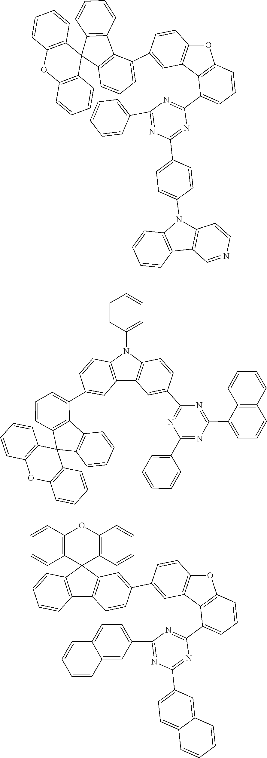
- the compound of Chemical Formula 1 is any one of the following structures.
- the second organic material layer is a hole blocking layer or an electron control layer.
- the first organic material layer is a light emitting layer
- the second organic material layer is a hole blocking layer or an electron control layer
- the light emitting layer and the hole blocking layer or the electron control layer are provided adjacent to each other.
- the second organic material layer is a hole blocking layer or an electron control layer
- the hole blocking layer or the electron control layer includes the compound of Chemical Formula 2.
- the second organic material layer includes the compound of Chemical Formula 2.
- At least one of X1 to X3 is N, and the rest are CR.
- R and Ar1 to Ar3 are the same as or different from each other, and each independently hydrogen; deuterium; a cyano group; a nitrile group; a substituted or unsubstituted trialkylsilyl group having 1 to 20 carbon atoms; a substituted or unsubstituted triarylsilyl group having 6 to 30 carbon atoms; a substituted or unsubstituted alkyl group having 1 to 20 carbon atoms; a substituted or unsubstituted haloalkyl group having 1 to 20 carbon atoms; a substituted or unsubstituted cycloalkyl group having 3 to 30 carbon atoms; a substituted or unsubstituted alkenyl group having 2 to 20 carbon atoms; a substituted or unsubstituted aryl group having 6 to 60 carbon atoms; or a substituted or unsubstituted heterocyclic group having 2 to 60 carbon atoms
- R and Ar1 to Ar3 are the same as or different from each other, and each independently hydrogen; deuterium; a cyano group; a nitrile group; a substituted or unsubstituted trialkylsilyl group having 1 to 20 carbon atoms; a substituted or unsubstituted triarylsilyl group having 6 to 30 carbon atoms; a substituted or unsubstituted alkyl group having 1 to 20 carbon atoms; a substituted or unsubstituted haloalkyl group having 1 to 20 carbon atoms; a substituted or unsubstituted cycloalkyl group having 3 to 30 carbon atoms; a substituted or unsubstituted alkenyl group having 2 to 20 carbon atoms; a substituted or unsubstituted aryl group having 6 to 60 carbon atoms; or a substituted or unsubstituted heterocyclic group having 2 to 60 carbon atoms and including one or
- R and Ar1 to Ar3 are the same as or different from each other, and each independently hydrogen; deuterium; a cyano group; a substituted or unsubstituted trialkylsilyl group having 1 to 20 carbon atoms; a substituted or unsubstituted triarylsilyl group having 6 to 30 carbon atoms; a substituted or unsubstituted haloalkyl group having 1 to 20 carbon atoms; a substituted or unsubstituted aryl group having 6 to 60 carbon atoms; or a substituted or unsubstituted heterocyclic group having 2 to 60 carbon atoms and including one or more of O, S, N and Si as a heteroatom, or Ar1 and R; or Ar2 and R bond to each other to form a substituted or unsubstituted aromatic hydrocarbon ring having 6 to 30 carbon atoms, and at least one of Ar1 to Ar3 is of the following Chemical Formula 3.
- R and Ar1 to Ar3 are the same as or different from each other, and each independently hydrogen; deuterium; a cyano group; a substituted or unsubstituted trifluoromethyl group; a substituted or unsubstituted phenyl group; a substituted or unsubstituted biphenyl group; a substituted or unsubstituted terphenyl group; a substituted or unsubstituted naphthyl group; a substituted or unsubstituted carbazolyl group; a substituted or unsubstituted triphenylenyl group; a substituted or unsubstituted dibenzothiophenyl group; a substituted or unsubstituted dibenzofuranyl group; a substituted or unsubstituted phenoxathiinyl group; a substituted or unsubstituted phenanthrenyl group; a substituted or unsubstituted
- * means a bonding position
- R and Ar1 to Ar3 may be unsubstituted or substituted with a substituent linking one or more of hydrogen; deuterium; a cyano group; a trifluoromethyl group; a trialkylsilyl group having 1 to 20 carbon atoms; a triarylsilyl group having 6 to 30 carbon atoms; an alkyl group having 1 to 20 carbon atoms; an aryl group having 6 to 30 carbon atoms; and a heterocyclic group having 2 to 30 carbon atoms and including one or more of O, S, N and Si as a heteroatom.
- R and Ar1 to Ar3 may be unsubstituted or substituted with a substituent linking one or more of hydrogen; deuterium; a cyano group; a trifluoromethyl group; a trialkylsilyl group having 1 to 10 carbon atoms; a triarylsilyl group having 6 to 20 carbon atoms; an alkyl group having 1 to 10 carbon atoms; an aryl group having 6 to 20; and a heterocyclic group having 2 to 20 carbon atoms and including one or more of O, S, N and Si as a heteroatom.
- R and Ar1 to Ar3 may be unsubstituted or substituted with a substituent linking one or more of hydrogen; deuterium; a cyano group; a trifluoromethyl group; a trimethylsilyl group; a triphenylsilyl group; a methyl group; a phenyl group; a biphenyl group; a naphthyl group, a dimethylfluorenyl group; a diphenylfluorenyl group; a dibenzofuranyl group; a dibenzothiophenyl group; and a carbazole group.
- R and Ar1 to Ar3 are the same as or different from each other, and each independently hydrogen; deuterium; a cyano group; a trifluoromethyl group; a phenyl group; a biphenyl group; a terphenyl group unsubstituted or substituted with a pyridyl group; a naphthyl group; a carbazolyl group unsubstituted or substituted with a methyl group or a phenyl group; a triphenylenyl group; a dibenzothiophenyl group unsubstituted or substituted with a methyl group; a dibenzofuranyl group; a phenoxathiinyl group; a phenanthrenyl group; a benzocarbazolyl group; a pyridyl group; an N-phenylindenocarbazolyl group unsubstituted or substituted with a methyl group; a trifluoromethyl
- * means a bonding position
- Ar1 and R; or Ar2 and R bond to each other to form substituted or unsubstituted benzene.
- Ar1 and R; or Ar2 and R bond to each other to form benzene unsubstituted or substituted with a benzocarbazole group.
- L11 to L13 are the same as or different from each other, and each independently a direct bond; a substituted or unsubstituted arylene group having 6 to 60 carbon atoms; or a substituted or unsubstituted divalent heterocyclic group having 2 to 60 carbon atoms.
- L11 to L13 are the same as or different from each other, and each independently a direct bond; a substituted or unsubstituted arylene group having 6 to 30 carbon atoms; or a substituted or unsubstituted divalent heterocyclic group having 2 to 30 carbon atoms and including one or more of O, S, N and Si as a heteroatom.
- L11 to L13 are the same as or different from each other, and each independently a direct bond; a substituted or unsubstituted phenylene group; a substituted or unsubstituted biphenylene group; a substituted or unsubstituted naphthylene group; a substituted or unsubstituted fluorenyl group; a substituted or unsubstituted divalent dibenzothiophene group; a substituted or unsubstituted divalent dibenzofuranyl group; a substituted or unsubstituted divalent carbazolyl group; a substituted or unsubstituted divalent benzocarbazolyl group; a substituted or unsubstituted divalent indenocarbazolyl group; a substituted or unsubstituted divalent dibenzosilole group; a substituted or unsubstituted divalent phenoxathiinyl group;
- * means a bonding position
- L11 to L13 are the same as or different from each other, and each independently a direct bond; a phenylene group unsubstituted or substituted with a methyl group, a phenyl group or a dibenzothiophenyl group; a biphenylene group; a naphthylene group; a dimethylfluorenyl group; a divalent dibenzothiophene group; a divalent dibenzofuranyl group; a divalent carbazolyl group unsubstituted or substituted with a phenyl group; a divalent benzocarbazolyl group unsubstituted or substituted with a phenyl group or a dimethylbiphenyl group; a divalent indenocarbazolyl group substituted with a methyl group; a divalent dimethyldibenzosilole group; a divalent phenoxathiinyl group; a divalent pyridyl group
- * means a bonding position
- one or two of Ar1 to Ar3 are of the following Chemical Formula 3.
- any one of R11 to R26 is linked to any one of L11 to L13, and the rest are hydrogen; a substituted or unsubstituted alkyl group having 1 to 20 carbon atoms; or a substituted or unsubstituted aryl group having 6 to 60 carbon atoms, or bond to adjacent groups to form a substituted or unsubstituted aromatic hydrocarbon ring having 6 to 30 carbon atoms.
- any one of R11 to R26 is linked to any one of L11 to L13, and the rest are hydrogen; a substituted or unsubstituted methyl group; a substituted or unsubstituted butyl group; a substituted or unsubstituted phenyl group; a substituted or unsubstituted naphthyl group; or a substituted or unsubstituted fluorenyl group, or bond to adjacent groups to form a substituted or unsubstituted benzene ring.
- any one of R11 to R26 is linked to any one of L11 to L13, and the rest are hydrogen; a methyl group; a tert-butyl group; an n-butyl group; a phenyl group unsubstituted or substituted with a methyl group; a naphthyl group; or a dimethylfluorenyl group, or bond to adjacent groups to form a benzene ring.
- any one of R11 to R18 is linked to any one of L11 to L13, and the rest are hydrogen; a methyl group; a tert-butyl group; an n-butyl group; a phenyl group unsubstituted or substituted with a methyl group; a naphthyl group; or a dimethylfluorenyl group, or bond to adjacent groups to form a benzene ring.
- any one of R19 to R26 is linked to any one of L11 to L13, and the rest are hydrogen; a methyl group; a tert-butyl group; an n-butyl group; a phenyl group unsubstituted or substituted with a methyl group; a naphthyl group; or a dimethylfluorenyl group, or bond to adjacent groups to form a benzene ring.
- Chemical Formula 2 is any one of the following Chemical Formulae 201 to 203.
- X1 to X3, Ar2 to Ar3, L11 to L13, m1 to m3 and R11 to R26 have the same definitions as in Chemical Formulae 2 and 3
- R31 and R32 have the same definitions as R11 to R26 in Chemical Formula 2
- r31 and r32 are an integer of 1 to 7.
- Chemical Formula 2 is any one of the following structures.
- the first organic material layer is a light emitting layer
- the light emitting layer includes the compound of Chemical Formula 1 described above, and a maximum light emission peak of the light emitting layer is from 400 nm to 500 nm.
- the organic light emitting device further includes one or more light emitting layers.
- the one or more light emitting layers may each include the fluorescent dopant or the phosphorescent dopant described above.
- the organic light emitting device further includes one or more light emitting layers having a maximum light emission peak appearing in a wavelength range different from a wavelength range of a maximum light emission peak that the light emitting layer including one or more types of the compound of Chemical Formula 1 has.
- a maximum light emission peak of the light emitting layer including one or more types of the compound of Chemical Formula 1 is from 400 nm to 500 nm, and the one or more light emitting layers having a maximum light emission peak appearing in a wavelength range different from a wavelength range of a maximum light emission peak that the light emitting layer including one or more types of the compound of Chemical Formula 1 has may have a maximum light emission peak appearing at 510 nm to 580 nm; or 610 nm to 680 nm.
- the first organic material layer of the organic light emitting device is a light emitting layer
- the light emitting layer includes the compound of Chemical Formula 1 described above and further includes a fluorescent dopant
- the organic light emitting device further includes one or more light emitting layers
- the one or more light emitting layers include a phosphorescent dopant.
- the organic light emitting device includes one or more light emitting layers having a maximum light emission peak appearing in a wavelength range that is the same as a wavelength range of a maximum light emission peak that the light emitting layer including one or more types of the compound of Chemical Formula 1 has.
- a maximum light emission peak of the light emitting layer is from 400 nm to 500 nm.
- the first organic material layer of the organic light emitting device is a light emitting layer
- the light emitting layer includes the compound of Chemical Formula 1 described above and further includes a fluorescent dopant
- the organic light emitting device further includes one or more light emitting layers
- the one or more light emitting layers include a fluorescent dopant.
- the organic light emitting device of the present disclosure includes two or more light emitting layers
- the two or more light emitting layers may be consecutively laminated in a vertical direction, or may be laminated side by side in a horizontal direction.
- FIGS. 1 to 4 each illustrate a laminated structure of the organic light emitting device of the present disclosure including two or more light emitting layers.
- FIG. 1 illustrates the organic light emitting device in which a substrate ( 0 ), a cathode ( 1 ), an electron transfer layer ( 2 ), a hole blocking layer or an electron control layer ( 7 ), a light emitting layer ( 101 ), a hole transfer layer ( 3 ) and an anode ( 4 ) are consecutively laminated, and, as the light emitting layer ( 101 ), a light emitting layer 1 ( 11 ) and a light emitting layer 2 ( 12 ) are laminated side by side in a horizontal direction.
- FIG. 2 illustrates the organic light emitting device in which a substrate ( 0 ), a cathode ( 1 ), an electron transfer layer ( 2 ), a hole blocking layer or an electron control layer ( 7 ), a light emitting layer 1 ( 11 ), an organic material layer ( 5 ), a light emitting layer 2 ( 12 ), a hole transfer layer ( 3 ) and an anode ( 4 ) are consecutively laminated in a vertical direction.
- FIG. 3 illustrates the organic light emitting device in which a substrate ( 0 ), a cathode ( 1 ), an electron transfer layer ( 2 ), a hole blocking layer or an electron control layer ( 7 ), a light emitting layer 1 ( 11 ), an organic material layer ( 5 ), a light emitting layer 2 ( 12 ), an organic material layer ( 6 ), a light emitting layer 3 ( 13 ), a hole transfer layer ( 3 ) and an anode ( 4 ) are consecutively laminated in a vertical direction.
- FIG. 4 illustrates the organic light emitting device in which a substrate ( 0 ), an anode ( 4 ), a hole injection layer ( 102 ), a hole transfer layer ( 103 ), a light emitting layer ( 101 ), a hole blocking layer or an electron control layer ( 104 ), an electron injection and transfer layer ( 105 ) and a cathode ( 1 ) are consecutively laminated in a vertical direction.
- Compounds having various energy band gaps may be synthesized in the present disclosure by introducing various substituents to the core structures of Chemical Formula 1 and Chemical Formula 2.
- HOMO and LUMO energy levels of the compound may also be controlled in the present disclosure by introducing various substituents to the core structures having structures as above.
- the organic light emitting device of the present disclosure may be manufactured using common organic light emitting device manufacturing methods and materials except that the first organic material layer is formed using the compound of Chemical Formula 1 described above, and the second organic material layer is formed using the compound of Chemical Formula 2 described above.
- a solution coating method may be used as well as a vacuum deposition method when forming the organic material layer.
- the solution coating method means spin coating, dip coating, inkjet printing, screen printing, a spray method, roll coating and the like, but is not limited thereto.
- the organic light emitting device of the present disclosure may be formed with one or more organic material layers among a hole transfer layer, a hole injection layer, an electron blocking layer, a hole control layer, a layer carrying out hole transfer and hole injection at the same time, a light emitting layer, an electron injection layer, an electron transfer layer, a hole blocking layer, an electron control layer, and a layer carrying out electron transfer and electron injection at the same time, and the first organic material layer is a light emitting layer and the second organic material layer is a hole blocking layer and/or an electron control layer.
- a structure of the organic light emitting device of the present specification is not limited thereto, and may include a larger number of organic material layers.
- the first electrode is an anode
- the second electrode is a cathode
- the first electrode is a cathode
- the second electrode is an anode
- the organic light emitting device may be manufactured by forming an anode on a substrate by depositing a metal, a metal oxide having conductivity, or an alloy thereof using a physical vapor deposition (PVD) method such as sputtering or e-beam evaporation, forming an organic material layer including one or more layers formed with a hole injection layer, a hole transfer layer, a light emitting layer, an electron blocking layer, an electron transfer layer, a layer carrying out hole transfer and hole injection at the same time, a hole blocking layer, a layer carrying out electron transfer and electron injection at the same time, and an electron injection layer, and then depositing a material capable of being used as a cathode thereon.
- the organic light emitting device may also be manufactured by consecutively depositing a cathode material, an organic material layer and an anode material on a substrate.
- the organic material layer may have a multilayer structure including a hole injection layer, a hole transfer layer, a layer carrying out hole injection and hole transfer at the same time, an electron blocking layer, a hole blocking layer, a light emitting layer, an electron transfer layer, an electron injection layer, a layer carrying out electron injection and electron transfer at the same time and the like, but is not limited thereto, and may have a single layer structure.
- the anode is an electrode injecting holes, and as the anode material, materials having large work function are normally preferred so that hole injection to an organic material layer is smooth.
- the anode material capable of being used in the present disclosure include metals such as vanadium, chromium, copper, zinc and gold, or alloys thereof; metal oxides such as zinc oxide, indium oxide, indium tin oxide (ITO) and indium zinc oxide (IZO); combinations of metals and oxides such as ZnO:Al or SnO 2 :Sb; conductive polymers such as poly(3-methylthiophene), poly[3,4-(ethylene-1,2-dioxy)thiophene] (PEDOT), polypyrrole and polyaniline, but are not limited thereto.
- the cathode is an electrode injecting electrons, and as the cathode material, materials having small work function are normally preferred so that electron injection to an organic material layer is smooth.
- the cathode material include metals such as magnesium, calcium, sodium, potassium, titanium, indium, yttrium, lithium, gadolinium, aluminum, silver, tin and lead, or alloys thereof; multilayer structure materials such as LiF/Al or LiO 2 /Al, and the like, but are not limited thereto.
- the cathode may be formed in one or two layers.
- the organic material layer may include an electron blocking layer, and as the electron blocking layer, materials known in the art may be used.
- the hole injection layer is a layer performing a role of smoothly injecting holes from an anode to a light emitting layer
- the hole injection material is a material capable of favorably receiving holes from an anode at a low voltage.
- the highest occupied molecular orbital (HOMO) of the hole injection material is preferably in between the work function of an anode material and the HOMO of surrounding organic material layers.
- the hole injection material examples include metal porphyrins, oligothiophene, arylamine-based organic materials, hexanitrile hexaazatriphenylene-based organic materials, quinacridone-based organic materials, perylene-based organic materials, anthraquinone, and polyaniline- and polythiophene-based conductive polymers, and the like, but are not limited thereto.
- the hole transfer layer may perform a role of smoothly transferring holes.
- the hole transfer material materials capable of receiving holes from an anode or a hole injection layer, moving the holes to a light emitting layer, and having high mobility for the holes are suited. Specific examples thereof include arylamine-based organic materials, conductive polymers, block copolymers having conjugated parts and non-conjugated parts together, and the like, but are not limited thereto.
- the light emitting layer may emit blue, green or red light, may be formed with a phosphorescent material or a fluorescent material, and the light emitting layer includes a host and a dopant.
- the host of the light emitting layer may include fused aromatic ring derivatives, heteroring-containing compounds or the like.
- fused aromatic ring derivative anthracene derivatives, pyrene derivatives, naphthalene derivatives, pentacene derivatives, phenanthrene compounds, fluoranthene compounds and the like may be included
- heteroring-containing compound carbazole derivatives, dibenzofuran derivatives, ladder-type furan compounds, pyrimidine derivatives and the like may be included, however, the host material is not limited thereto, and the compound of Chemical Formula 1 described above may be used.
- phosphorescent materials such as bis(1-phenylisoquinoline)acetylacetonate iridium (PIQIr(acac)), bis(1-phenylquinoline)acetylacetonate iridium (PQIr(acac)), tris(1-phenylquinoline)iridium (PQIr) or octaethylporphyrin platinum (PtOEP), or fluorescent materials such as tris(8-hydroxyquinolino)aluminum (Alq 3 ) may be used as the light emitting dopant, however, the light emitting dopant is not limited thereto.
- phosphorescent materials such as fac tris(2-phenylpyridine)iridium (Ir(ppy) 3 ), or fluorescent materials such as tris(8-hydroxyquinolino)aluminum (Alq 3 ) may be used as the light emitting dopant, however, the light emitting dopant is not limited thereto.
- phosphorescent materials such as (4,6-F2ppy) 2 Irpic, or fluorescent materials such as spiro-DPVBi, spiro-6P, distyrylbenzene (DSB), distyrylarylene (DSA), PFO-based polymers or PPV-based polymers may be used as the light emitting dopant, however, the light emitting dopant is not limited thereto.
- the electron transfer layer may perform a role of smoothly transferring electrons.
- the electron transfer material materials capable of favorably receiving electrons from a cathode, moving the electrons to a light emitting layer, and having high mobility for the electrons are suited. Specific examples thereof include Al complexes of 8-hydroxyquinoline; complexes including Alq 3 ; organic radical compounds; hydroxyflavon-metal complexes, and the like, but are not limited thereto.
- the electron injection layer may perform a role of smoothly injecting electrons.
- the electron injection material compounds having an electron transferring ability, having an electron injection effect from a cathode, having an excellent electron injection effect for a light emitting layer or light emitting material, and preventing excitons generated in the light emitting layer from moving to a hole injection layer, and in addition thereto, having an excellent thin film forming ability are preferred.
- fluorenone anthraquinodimethane, diphenoquinone, thiopyran dioxide, oxazole, oxadiazole, triazole, imidazole, perylene tetracarboxylic acid, fluorenylidene methane, anthrone or the like, and derivatives thereof, metal complex compounds, nitrogen-containing 5-membered ring derivatives, and the like, but are not limited thereto.
- the metal complex compound includes 8-hydroxyquinolinato lithium, bis(8-hydroxyquinolinato)zinc, bis(8-hydroxyquinolinato)copper, bis(8-hydroxyquinolinato)manganese, tris(8-hydroxyquinolinato)aluminum, tris(2-methyl-8-hydroxyquinolinato)aluminum, tris(8-hydroxyquinolinato)gallium, bis(10-hydroxybenzo[h]quinolinato)beryllium, bis(10-hydroxybenzo[h]quinolinato)zinc, bis(2-methyl-8-quinolinato)chlorogallium, bis(2-methyl-8-quinolinato) (o-cresolato)gallium, bis(2-methyl-8-quinolinato) (1-naphtholato)aluminum, bis(2-methyl-8-quinolinato) (2-naphtholato)gallium and the like, but is not limited thereto.
- the hole blocking layer is a layer blocking holes from reaching a cathode, may be provided between an electron transfer layer and a light emitting layer, and may be generally formed under the same condition as a hole injection layer. Specific examples thereof may include oxadiazole derivatives, triazole derivatives, phenanthroline derivatives, BCP, aluminum complexes and the like, however, the compound of Chemical Formula 2 described above may be used.
- the electron control layer is a layer controlling electron migration to a light emitting layer, and materials known in the art may be used, and the compound of Chemical Formula 2 described above may be used.
- the hole control layer is a layer controlling hole migration to a light emitting layer, and materials known in the art may be used.
- the organic light emitting device may be a top-emission type, a bottom-emission type or a dual-emission type depending on the materials used.
- a glass substrate (corning 7059 glass) on which indium tin oxide (ITO) was coated as a thin film to a thickness of 1000 ⁇ was placed in dispersant-dissolved distilled water and ultrasonic cleaned.
- ITO indium tin oxide
- a product of Fischer Co. was used as the detergent, and as the distilled water, distilled water filtered twice with a filter manufactured by Millipore Co. was used. After the ITO was cleaned for 30 minutes, ultrasonic cleaning was repeated twice using distilled water for 10 minutes. After the cleaning with distilled water was finished, the substrate was ultrasonic cleaned with solvents of isopropyl alcohol, acetone and methanol in this order, and then dried.
- HAT-CN hexanitrile hexaazatriphenylene
- Compound 2-1 of Example 1 of Table 1 was deposited to a thickness of 50 ⁇ as a hole blocking layer (electron control layer), and then Compound ET1 and lithium quinolate (LiQ) were vacuum deposited in a weight ratio of 1:1 to form an electron injection and transfer layer to a thickness of 350 ⁇ .
- a cathode was formed by consecutively depositing lithium fluoride (LiF) and aluminum to a thickness of 12 ⁇ and 2,000 ⁇ , respectively, and as a result, an organic light emitting device was manufactured.
- the deposition rates of the organic materials were maintained at 0.4 ⁇ /sec to 0.7 ⁇ /sec, the deposition rates of the lithium fluoride and the aluminum of the cathode were maintained at 0.3 ⁇ /sec and 2 ⁇ /sec, respectively, and the degree of vacuum during the deposition was maintained at 2 ⁇ 10 ⁇ 7 torr to 5 ⁇ 10 ⁇ 6 torr.
- Organic light emitting devices were manufactured in the same manner as in Example 1-1 except that Compounds 2-2 to 2-7 were used instead of 2-1.
- Organic light emitting devices were manufactured in the same manner as in Example 1-1 except that Compounds BH2 to BH4 were used instead of Compound BH1.
- Organic light emitting devices were manufactured in the same manner as in Example 1-1 except that compounds of the following Table 1 were used instead of Compound BH1, and compounds of the following Table 1 were used instead of Compound 2-1.
- LT98 means time taken for luminance decreasing to 98% from initial luminance.
- Examples 1-1 to 1-7 and 2-1 to 2-3 used the compound of Chemical Formula 1 of the present application in which dibenzofuran bonds to anthracene as a host of a light emitting layer, and used the compound of Chemical Formula 2 in which an N-including heterocyclic group bonds to spirofluorenexanthene in a hole blocking layer.
- Comparative Examples 1 to 8 used an anthracene compound in which only an aryl group bonds thereto as a host of a light emitting layer instead of the compound of Chemical Formula 1 of the present application, or used a compound in which an N-including heterocyclic group bonds to diphenylfluorene as a material of a hole blocking layer instead of the compound of Chemical Formula 2 of the present application.
- Examples 1-1 to 1-7 and 2-1 to 2-3 had properties of low driving voltage, high efficiency and long lifetime compared to when using only one of the compounds of Chemical Formulae 1 and 2.
Landscapes
- Physics & Mathematics (AREA)
- Spectroscopy & Molecular Physics (AREA)
- Chemical & Material Sciences (AREA)
- Engineering & Computer Science (AREA)
- Materials Engineering (AREA)
- Optics & Photonics (AREA)
- Electroluminescent Light Sources (AREA)
Abstract

Description

-
- L1 and L2 are the same as or different from each other, and each independently a direct bond; or a substituted or unsubstituted arylene group,
- R1 and R2 are the same as or different from each other, and each independently hydrogen; deuterium; a halogen group; a cyano group; a nitro group; a substituted or unsubstituted alkyl group; a substituted or unsubstituted haloalkyl group; a substituted or unsubstituted haloalkoxy group; a substituted or unsubstituted cycloalkyl group; a substituted or unsubstituted alkenyl group; a substituted or unsubstituted aryl group; or a substituted or unsubstituted heterocyclic group, or bond to adjacent groups to form a substituted or unsubstituted ring,
- n1 is an integer of 0 to 7, and when n1 is 2 or greater, the two or more R1s are the same as or different from each other,
- n2 is an integer of 0 to 9, and when n2 is 2 or greater, the two or more -L2-R2s are the same as or different from each other, and
- n3 is 1 or 2, and when n3 is 2, substituents in the two parentheses are the same as or different from each other, and 1≤n2+n3≤10,

-
- in Chemical Formula 2,
- at least one of X1 to X3 is N, and the rest are CR,
- R and Ar1 to Ar3 are the same as or different from each other, and each independently hydrogen; deuterium; a cyano group; a nitrile group; a substituted or unsubstituted silyl group; a substituted or unsubstituted alkyl group; a substituted or unsubstituted haloalkyl group; a substituted or unsubstituted cycloalkyl group; a substituted or unsubstituted alkenyl group; a substituted or unsubstituted aryl group; or a substituted or unsubstituted heterocyclic group, or bond to adjacent groups to form a substituted or unsubstituted ring, and at least one of Ar1 to Ar3 is of the following Chemical Formula 3,
- L11 to L13 are the same as or different from each other, and each independently a direct bond; a substituted or unsubstituted arylene group; or a substituted or unsubstituted divalent heterocyclic group, and
- m1 to m3 are each an integer of 0 to 3, and when m1 to m3 are each 2 or greater, substituents in the two or more parentheses are the same as or different from each other,

-
- in Chemical Formula 3,
- any one of R11 to R26 is linked to any one of L11 to L13, and the rest are hydrogen; deuterium; a cyano group; a nitrile group; a substituted or unsubstituted alkyl group; a substituted or unsubstituted cycloalkyl group; a substituted or unsubstituted alkenyl group; a substituted or unsubstituted aryl group; or a substituted or unsubstituted heterocyclic group, or bond to adjacent groups to form a substituted or unsubstituted ring.
-
- 0: Substrate
- 1: Cathode
- 2: Electron Transfer Layer
- 3: Hole Transfer Layer
- 4: Anode
- 5: Organic Material Layer
- 6: Organic Material Layer
- 7: Hole Blocking Layer or Electron Control Layer
- 11:
Light Emitting Layer 1 - 12:
Light Emitting Layer 2 - 13:
Light Emitting Layer 3 - 101: Light Emitting Layer
- 102: Hole Injection Layer
- 103: Hole Transfer Layer
- 104: Hole Blocking Layer or Electron Control Layer
- 105: Electron Injection and Transfer Layer

-
- L1 and L2 are the same as or different from each other, and each independently a direct bond; or a substituted or unsubstituted arylene group,
- R1 and R2 are the same as or different from each other, and each independently hydrogen; deuterium; a halogen group; a cyano group; a nitro group; a substituted or unsubstituted alkyl group; a substituted or unsubstituted haloalkyl group; a substituted or unsubstituted haloalkoxy group; a substituted or unsubstituted cycloalkyl group; a substituted or unsubstituted alkenyl group; a substituted or unsubstituted aryl group; or a substituted or unsubstituted heterocyclic group, or bond to adjacent groups to form a substituted or unsubstituted ring,
- n1 is an integer of 0 to 7, and when n1 is 2 or greater, the two or more R1s are the same as or different from each other,
- n2 is an integer of 0 to 9, and when n2 is 2 or greater, the two or more -L2-R2s are the same as or different from each other, and
- n3 is 1 or 2, and when n3 is 2, substituents in the two parentheses are the same as or different from each other, and 1≤n2+n3≤10,

-
- in
Chemical Formula 2, - at least one of X1 to X3 is N, and the rest are CR,
- R and Ar1 to Ar3 are the same as or different from each other, and each independently hydrogen; deuterium; a cyano group; a nitrile group; a substituted or unsubstituted silyl group; a substituted or unsubstituted alkyl group; a substituted or unsubstituted haloalkyl group; a substituted or unsubstituted cycloalkyl group; a substituted or unsubstituted alkenyl group; a substituted or unsubstituted aryl group; or a substituted or unsubstituted heterocyclic group, or bond to adjacent groups to form a substituted or unsubstituted ring, and at least one of Ar1 to Ar3 is of the following
Chemical Formula 3, - L11 to L13 are the same as or different from each other, and each independently a direct bond; a substituted or unsubstituted arylene group; or a substituted or unsubstituted divalent heterocyclic group, and
- m1 to m3 are each an integer of 0 to 3, and when m1 to m3 are each 2 or greater, substituents in the two or more parentheses are the same as or different from each other,
- in

-
- in
Chemical Formula 3, - any one of R11 to R26 is linked to any one of L11 to L13, and the rest are hydrogen; deuterium; a cyano group; a nitrile group; a substituted or unsubstituted alkyl group; a substituted or unsubstituted cycloalkyl group; a substituted or unsubstituted alkenyl group; a substituted or unsubstituted aryl group; or a substituted or unsubstituted heterocyclic group, or bond to adjacent groups to form a substituted or unsubstituted ring.
- in

and

and a substituted fluorenyl group such as

(9,9-dimethylfluorenyl group) and

(9,9-diphenylfluorenyl group) may be included, however, the structure is not limited thereto.

-
- L31 and L32 are the same as or different from each other, and each independently a direct bond; substituted or unsubstituted arylene having 6 to 60 carbon atoms; or substituted or unsubstituted heteroarylene having 2 to 60 carbon atoms and including any one or more heteroatoms selected from the group consisting of N, O and S,
- Ar31 and Ar32 are the same as or different from each other, and each independently substituted or unsubstituted aryl having 6 to 60 carbon atoms; or substituted or unsubstituted heteroaryl having 2 to 60 carbon atoms and including any one or more heteroatoms selected from the group consisting of N, O and S,

-
- in Chemical Formula B,
- L33, L34 and L35 are each independently a direct bond; substituted or unsubstituted arylene having 6 to 60 carbon atoms; or substituted or unsubstituted heteroarylene having 2 to 60 carbon atoms and including any one or more heteroatoms selected from the group consisting of N, O and S, and
- Ar33, Ar34 and Ar35 are each independently substituted or unsubstituted aryl having 6 to 60 carbon atoms; or substituted or unsubstituted heteroaryl having 2 to 60 carbon atoms and including any one or more heteroatoms selected from the group consisting of N, O and S.


-
- any one of R11 to R26 is linked to any one of L11 to L13, and the rest are hydrogen; deuterium; a cyano group; a nitrile group; a substituted or unsubstituted alkyl group; a substituted or unsubstituted cycloalkyl group; a substituted or unsubstituted alkenyl group; a substituted or unsubstituted aryl group; or a substituted or unsubstituted heterocyclic group, or bond to adjacent groups to form a substituted or unsubstituted ring.


| TABLE 1 | |||||
| First | Second | ||||
| Organic | Organic | ||||
| Material | Material | ||||
| Layer (Light | Layer (Hole | ||||
| Emitting | Blocking | Voltage | Efficiency | LT98 | |
| Layer Host) | Layer) | (V) | (cd/A) | (hr) | |
| Example 1-1 | BH1 | 2-1 | 3.74 | 5.25 | 49 |
| Example 1-2 | BH1 | 2-2 | 3.99 | 4.92 | 68 |
| Example 1-3 | BH1 | 2-3 | 3.92 | 5.12 | 58 |
| Example 1-4 | BH1 | 2-4 | 3.90 | 5.30 | 49 |
| Example 1-5 | BH1 | 2-5 | 4.12 | 4.77 | 76 |
| Example 1-6 | BH1 | 2-6 | 4.15 | 4.70 | 74 |
| Example 1-7 | BH1 | 2-7 | 4.01 | 5.31 | 59 |
| Example 2-1 | BH2 | 2-1 | 3.81 | 4.91 | 61 |
| Example 2-2 | BH3 | 2-1 | 4.11 | 4.50 | 65 |
| Example 2-3 | BH4 | 2-1 | 3.84 | 5.28 | 44 |
| Comparative | BH1 | (No Second | 5.45 | 2.58 | 22 |
| Example 1 | Organic | ||||
| Material | |||||
| Layer) | |||||
| Comparative | — | 2-1 | 5.29 | 3.20 | 32 |
| Example 2 | |||||
| Comparative | 2-1 | BH1 | 4.83 | 4.44 | 34 |
| Example 3 | |||||
| Comparative | BH5 | ET2 | 4.23 | 3.59 | 19 |
| Example 4 | |||||
| Comparative | ET2 | BH5 | 7.08 | 1.05 | 5 |
| Example 5 | |||||
| Comparative | BH1 | ET2 | 4.31 | 3.92 | 38 |
| Example 6 | |||||
| Comparative | BH5 | 2-1 | 4.31 | 4.45 | 20 |
| Example 7 | |||||
| Comparative | BH5 | 2-4 | 4.38 | 4.41 | 21 |
| Example 8 | |||||
Claims (11)


Applications Claiming Priority (3)
| Application Number | Priority Date | Filing Date | Title |
|---|---|---|---|
| KR20180086643 | 2018-07-25 | ||
| KR10-2018-0086643 | 2018-07-25 | ||
| PCT/KR2019/009259 WO2020022811A1 (en) | 2018-07-25 | 2019-07-25 | Organic light emitting device |
Publications (2)
| Publication Number | Publication Date |
|---|---|
| US20210217967A1 US20210217967A1 (en) | 2021-07-15 |
| US12004423B2 true US12004423B2 (en) | 2024-06-04 |
Family
ID=69180989
Family Applications (1)
| Application Number | Title | Priority Date | Filing Date |
|---|---|---|---|
| US17/057,419 Active 2041-11-05 US12004423B2 (en) | 2018-07-25 | 2019-07-25 | Organic light emitting device |
Country Status (4)
| Country | Link |
|---|---|
| US (1) | US12004423B2 (en) |
| KR (1) | KR102200025B1 (en) |
| CN (2) | CN119855470A (en) |
| WO (1) | WO2020022811A1 (en) |
Families Citing this family (7)
| Publication number | Priority date | Publication date | Assignee | Title |
|---|---|---|---|---|
| KR102138410B1 (en) * | 2017-06-30 | 2020-07-27 | 주식회사 엘지화학 | Organic light emitting device |
| US12435073B2 (en) | 2019-08-19 | 2025-10-07 | Idemitsu Kosan Co., Ltd. | Compound, material for organic electroluminescent element, organic electroluminescent element, and electronic device |
| KR102875402B1 (en) * | 2020-07-16 | 2025-10-22 | 주식회사 엘지화학 | Heterocyclic compound and organic light emitting device comprising the same |
| KR20220052384A (en) * | 2020-10-19 | 2022-04-28 | 삼성디스플레이 주식회사 | light emitting device and electronic apparatus including the light emitting device |
| CN114685419B (en) * | 2020-12-29 | 2024-10-29 | 北京绿人科技有限责任公司 | Organic compound containing spiro structure and organic electroluminescent device |
| CN116144346A (en) * | 2021-11-16 | 2023-05-23 | 浙江虹舞科技有限公司 | Composition for organic electroluminescent device and organic electroluminescent device comprising same |
| KR20240019581A (en) * | 2022-08-04 | 2024-02-14 | 주식회사 엘지화학 | Organic light emitting device |
Citations (14)
| Publication number | Priority date | Publication date | Assignee | Title |
|---|---|---|---|---|
| KR20080095244A (en) | 2006-02-07 | 2008-10-28 | 스미또모 가가꾸 가부시키가이샤 | Organic electroluminescent element |
| KR101593368B1 (en) | 2015-04-22 | 2016-02-11 | 주식회사 엘지화학 | Hetero-cyclic compound and organic light emitting diode comprising the same |
| KR20160141359A (en) | 2015-05-27 | 2016-12-08 | 삼성디스플레이 주식회사 | Organic light-emitting device |
| KR20160141361A (en) | 2015-05-27 | 2016-12-08 | 삼성디스플레이 주식회사 | Organic light-emitting device |
| KR20170032414A (en) | 2014-07-21 | 2017-03-22 | 메르크 파텐트 게엠베하 | Materials for electronic devices |
| KR101755986B1 (en) | 2016-02-23 | 2017-07-07 | 주식회사 엘지화학 | Hetero-cyclic compound and organic light emitting device comprising the same |
| KR20170134264A (en) | 2016-05-27 | 2017-12-06 | 주식회사 엘지화학 | Organic light emitting device |
| KR20180022190A (en) | 2016-08-23 | 2018-03-06 | 주식회사 두산 | Organic compounds and organic electro luminescence device comprising the same |
| KR20180037695A (en) | 2016-10-05 | 2018-04-13 | 에스에프씨 주식회사 | Organic light-emitting diode with long lifetime, low voltage and high efficiency |
| KR20180069423A (en) | 2016-12-15 | 2018-06-25 | (주)씨엠디엘 | Spirofluorenexanthenyl derivatives and organic electroluminescent device including the same |
| KR20180103021A (en) | 2017-03-08 | 2018-09-18 | 주식회사 엘지화학 | Organic light emitting device |
| KR20180111558A (en) | 2017-03-30 | 2018-10-11 | 주식회사 엘지화학 | Organic light emitting device |
| US20190214572A1 (en) * | 2016-09-29 | 2019-07-11 | Rohm And Haas Electronic Materials Korea Ltd | Organic electroluminescent device comprising electrontransport layer and electron buffer layer |
| US10367147B2 (en) | 2015-05-27 | 2019-07-30 | Samsung Display Co., Ltd. | Organic light-emitting device |
Family Cites Families (2)
| Publication number | Priority date | Publication date | Assignee | Title |
|---|---|---|---|---|
| US20160211454A1 (en) * | 2015-01-20 | 2016-07-21 | Samsung Display Co., Ltd. | Organic light-emitting device |
| KR20170039020A (en) * | 2015-09-30 | 2017-04-10 | 주식회사 스킨앤스킨 | Organic electroluminescent compound and organic electroluminescent device |
-
2019
- 2019-07-25 US US17/057,419 patent/US12004423B2/en active Active
- 2019-07-25 KR KR1020190090269A patent/KR102200025B1/en active Active
- 2019-07-25 CN CN202411881240.7A patent/CN119855470A/en active Pending
- 2019-07-25 WO PCT/KR2019/009259 patent/WO2020022811A1/en not_active Ceased
- 2019-07-25 CN CN201980033886.0A patent/CN112154548B/en active Active
Patent Citations (18)
| Publication number | Priority date | Publication date | Assignee | Title |
|---|---|---|---|---|
| US20090174315A1 (en) | 2006-02-07 | 2009-07-09 | Sumitomo Chemical Company Limited | Organic electroluminescent element |
| KR20080095244A (en) | 2006-02-07 | 2008-10-28 | 스미또모 가가꾸 가부시키가이샤 | Organic electroluminescent element |
| KR20170032414A (en) | 2014-07-21 | 2017-03-22 | 메르크 파텐트 게엠베하 | Materials for electronic devices |
| KR101593368B1 (en) | 2015-04-22 | 2016-02-11 | 주식회사 엘지화학 | Hetero-cyclic compound and organic light emitting diode comprising the same |
| US10367147B2 (en) | 2015-05-27 | 2019-07-30 | Samsung Display Co., Ltd. | Organic light-emitting device |
| KR20160141359A (en) | 2015-05-27 | 2016-12-08 | 삼성디스플레이 주식회사 | Organic light-emitting device |
| KR20160141361A (en) | 2015-05-27 | 2016-12-08 | 삼성디스플레이 주식회사 | Organic light-emitting device |
| KR101755986B1 (en) | 2016-02-23 | 2017-07-07 | 주식회사 엘지화학 | Hetero-cyclic compound and organic light emitting device comprising the same |
| KR20170134264A (en) | 2016-05-27 | 2017-12-06 | 주식회사 엘지화학 | Organic light emitting device |
| KR20180022190A (en) | 2016-08-23 | 2018-03-06 | 주식회사 두산 | Organic compounds and organic electro luminescence device comprising the same |
| US20190214572A1 (en) * | 2016-09-29 | 2019-07-11 | Rohm And Haas Electronic Materials Korea Ltd | Organic electroluminescent device comprising electrontransport layer and electron buffer layer |
| KR20180037695A (en) | 2016-10-05 | 2018-04-13 | 에스에프씨 주식회사 | Organic light-emitting diode with long lifetime, low voltage and high efficiency |
| EP3524660A1 (en) | 2016-10-05 | 2019-08-14 | SFC Co., Ltd. | Organic light-emitting device having long life, low voltage and high efficiency |
| KR20180069423A (en) | 2016-12-15 | 2018-06-25 | (주)씨엠디엘 | Spirofluorenexanthenyl derivatives and organic electroluminescent device including the same |
| KR20180103021A (en) | 2017-03-08 | 2018-09-18 | 주식회사 엘지화학 | Organic light emitting device |
| US20190296243A1 (en) * | 2017-03-08 | 2019-09-26 | Lg Chem, Ltd. | Organic light emitting device |
| KR20180111558A (en) | 2017-03-30 | 2018-10-11 | 주식회사 엘지화학 | Organic light emitting device |
| US20190214571A1 (en) | 2017-03-30 | 2019-07-11 | Lg Chem, Ltd. | Organic light emitting device |
Also Published As
| Publication number | Publication date |
|---|---|
| KR102200025B1 (en) | 2021-01-08 |
| CN112154548A (en) | 2020-12-29 |
| CN119855470A (en) | 2025-04-18 |
| WO2020022811A1 (en) | 2020-01-30 |
| KR20200011912A (en) | 2020-02-04 |
| US20210217967A1 (en) | 2021-07-15 |
| CN112154548B (en) | 2025-01-28 |
Similar Documents
| Publication | Publication Date | Title |
|---|---|---|
| US11631821B2 (en) | Polycyclic aromatic compounds containing a 1,11-dioxa-,1,11-dithia-, or 1-oxa-11-thia-4,8-diaza-11b-boradicyclopenta[a,j]phenalene core and organic light-emitting device comprising same | |
| US12004423B2 (en) | Organic light emitting device | |
| US12016243B2 (en) | Condensed cyclic compound and organic light emitting device comprising same | |
| US11845768B2 (en) | Polycyclic compound and organic light-emitting device including same | |
| US10686138B2 (en) | Compound and organic light emitting diode comprising same | |
| US11251377B2 (en) | Organic light emitting device | |
| US11718606B2 (en) | Polycyclic compound and organic light emitting element comprising same | |
| US20190148650A1 (en) | Organic Light Emitting Device | |
| US20220352473A1 (en) | Polycyclic compound and organic light emitting diode comprising same | |
| US12563964B2 (en) | Organic light-emitting device | |
| US20240309270A1 (en) | Compound and organic light-emitting device comprising same | |
| US12497415B2 (en) | Polycyclic compound and organic light-emitting element comprising same | |
| US20210217963A1 (en) | Organic light-emitting device | |
| US11367838B2 (en) | Anthracene derivative and organic light-emitting device comprising same | |
| US20220310935A1 (en) | Organic light-emitting device | |
| US12133455B2 (en) | Polycyclic compound and organic light emitting diode comprising same | |
| US11396494B2 (en) | Compound and organic light emitting element comprising same | |
| US11802124B2 (en) | Compound and organic light emitting diode comprising same | |
| US20250255093A1 (en) | Compound and organic light-emitting element comprising same | |
| US9960357B2 (en) | Spiro-type compound and organic light emitting element comprising same | |
| US20210351360A1 (en) | Heterocyclic compound and organic light emitting device comprising same | |
| US20230257356A1 (en) | Benzimidazole-substituted fluoranthene compound, and organic light emitting device including the same | |
| US12041851B2 (en) | Compound and organic light emitting device comprising same | |
| US12180177B2 (en) | Compound and organic light emitting diode comprising same | |
| US20240381763A1 (en) | Novel compound and organic light emitting device comprising the same |
Legal Events
| Date | Code | Title | Description |
|---|---|---|---|
| AS | Assignment |
Owner name: LG CHEM, LTD., KOREA, REPUBLIC OF Free format text: ASSIGNMENT OF ASSIGNORS INTEREST;ASSIGNORS:HUH, JUNGOH;HONG, SUNG KIL;HEO, DONG UK;AND OTHERS;SIGNING DATES FROM 20200203 TO 20200208;REEL/FRAME:054433/0070 |
|
| FEPP | Fee payment procedure |
Free format text: ENTITY STATUS SET TO UNDISCOUNTED (ORIGINAL EVENT CODE: BIG.); ENTITY STATUS OF PATENT OWNER: LARGE ENTITY |
|
| STPP | Information on status: patent application and granting procedure in general |
Free format text: APPLICATION DISPATCHED FROM PREEXAM, NOT YET DOCKETED |
|
| STPP | Information on status: patent application and granting procedure in general |
Free format text: DOCKETED NEW CASE - READY FOR EXAMINATION |
|
| STPP | Information on status: patent application and granting procedure in general |
Free format text: NON FINAL ACTION MAILED |
|
| STPP | Information on status: patent application and granting procedure in general |
Free format text: RESPONSE TO NON-FINAL OFFICE ACTION ENTERED AND FORWARDED TO EXAMINER |
|
| STPP | Information on status: patent application and granting procedure in general |
Free format text: NOTICE OF ALLOWANCE MAILED -- APPLICATION RECEIVED IN OFFICE OF PUBLICATIONS |
|
| ZAAB | Notice of allowance mailed |
Free format text: ORIGINAL CODE: MN/=. |
|
| STPP | Information on status: patent application and granting procedure in general |
Free format text: PUBLICATIONS -- ISSUE FEE PAYMENT VERIFIED |
|
| STCF | Information on status: patent grant |
Free format text: PATENTED CASE |