US11991893B2 - Display device having an auxiliary electrode including a concave portion or a convex portion - Google Patents
Display device having an auxiliary electrode including a concave portion or a convex portion Download PDFInfo
- Publication number
- US11991893B2 US11991893B2 US17/532,861 US202117532861A US11991893B2 US 11991893 B2 US11991893 B2 US 11991893B2 US 202117532861 A US202117532861 A US 202117532861A US 11991893 B2 US11991893 B2 US 11991893B2
- Authority
- US
- United States
- Prior art keywords
- auxiliary electrode
- layer
- electrode
- convex portion
- region
- Prior art date
- Legal status (The legal status is an assumption and is not a legal conclusion. Google has not performed a legal analysis and makes no representation as to the accuracy of the status listed.)
- Active, expires
Links
Images


Classifications
-
- H—ELECTRICITY
- H10—SEMICONDUCTOR DEVICES; ELECTRIC SOLID-STATE DEVICES NOT OTHERWISE PROVIDED FOR
- H10K—ORGANIC ELECTRIC SOLID-STATE DEVICES
- H10K59/00—Integrated devices, or assemblies of multiple devices, comprising at least one organic light-emitting element covered by group H10K50/00
- H10K59/10—OLED displays
- H10K59/12—Active-matrix OLED [AMOLED] displays
- H10K59/122—Pixel-defining structures or layers, e.g. banks
-
- H—ELECTRICITY
- H10—SEMICONDUCTOR DEVICES; ELECTRIC SOLID-STATE DEVICES NOT OTHERWISE PROVIDED FOR
- H10K—ORGANIC ELECTRIC SOLID-STATE DEVICES
- H10K50/00—Organic light-emitting devices
- H10K50/10—OLEDs or polymer light-emitting diodes [PLED]
- H10K50/14—Carrier transporting layers
- H10K50/16—Electron transporting layers
-
- H—ELECTRICITY
- H10—SEMICONDUCTOR DEVICES; ELECTRIC SOLID-STATE DEVICES NOT OTHERWISE PROVIDED FOR
- H10K—ORGANIC ELECTRIC SOLID-STATE DEVICES
- H10K50/00—Organic light-emitting devices
- H10K50/80—Constructional details
- H10K50/805—Electrodes
- H10K50/81—Anodes
- H10K50/814—Anodes combined with auxiliary electrodes, e.g. ITO layer combined with metal lines
-
- H—ELECTRICITY
- H10—SEMICONDUCTOR DEVICES; ELECTRIC SOLID-STATE DEVICES NOT OTHERWISE PROVIDED FOR
- H10K—ORGANIC ELECTRIC SOLID-STATE DEVICES
- H10K50/00—Organic light-emitting devices
- H10K50/80—Constructional details
- H10K50/805—Electrodes
- H10K50/82—Cathodes
- H10K50/824—Cathodes combined with auxiliary electrodes
-
- H—ELECTRICITY
- H10—SEMICONDUCTOR DEVICES; ELECTRIC SOLID-STATE DEVICES NOT OTHERWISE PROVIDED FOR
- H10K—ORGANIC ELECTRIC SOLID-STATE DEVICES
- H10K59/00—Integrated devices, or assemblies of multiple devices, comprising at least one organic light-emitting element covered by group H10K50/00
- H10K59/10—OLED displays
- H10K59/12—Active-matrix OLED [AMOLED] displays
- H10K59/131—Interconnections, e.g. wiring lines or terminals
-
- H—ELECTRICITY
- H10—SEMICONDUCTOR DEVICES; ELECTRIC SOLID-STATE DEVICES NOT OTHERWISE PROVIDED FOR
- H10K—ORGANIC ELECTRIC SOLID-STATE DEVICES
- H10K59/00—Integrated devices, or assemblies of multiple devices, comprising at least one organic light-emitting element covered by group H10K50/00
- H10K59/80—Constructional details
- H10K59/805—Electrodes
- H10K59/8052—Cathodes
- H10K59/80522—Cathodes combined with auxiliary electrodes
-
- H—ELECTRICITY
- H10—SEMICONDUCTOR DEVICES; ELECTRIC SOLID-STATE DEVICES NOT OTHERWISE PROVIDED FOR
- H10K—ORGANIC ELECTRIC SOLID-STATE DEVICES
- H10K71/00—Manufacture or treatment specially adapted for the organic devices covered by this subclass
-
- H—ELECTRICITY
- H10—SEMICONDUCTOR DEVICES; ELECTRIC SOLID-STATE DEVICES NOT OTHERWISE PROVIDED FOR
- H10K—ORGANIC ELECTRIC SOLID-STATE DEVICES
- H10K59/00—Integrated devices, or assemblies of multiple devices, comprising at least one organic light-emitting element covered by group H10K50/00
- H10K59/10—OLED displays
- H10K59/12—Active-matrix OLED [AMOLED] displays
- H10K59/121—Active-matrix OLED [AMOLED] displays characterised by the geometry or disposition of pixel elements
-
- H—ELECTRICITY
- H10—SEMICONDUCTOR DEVICES; ELECTRIC SOLID-STATE DEVICES NOT OTHERWISE PROVIDED FOR
- H10K—ORGANIC ELECTRIC SOLID-STATE DEVICES
- H10K59/00—Integrated devices, or assemblies of multiple devices, comprising at least one organic light-emitting element covered by group H10K50/00
- H10K59/30—Devices specially adapted for multicolour light emission
- H10K59/35—Devices specially adapted for multicolour light emission comprising red-green-blue [RGB] subpixels
Definitions
- the present disclosure relates to a display device and a manufacturing method thereof.
- An organic light emitting device (hereinafter, referred to as a light emitting device) constituting organic light emitting diodes (OLEDs) emits light by itself without a separate light source (e.g., no backlight needed), and thus, the OLED display device can be thinner and lighter. Also, the OLED display device shows high quality characteristics, such as low power consumption, a high luminance, and high response speed, etc.
- the light emitting device has a structure in which an anode electrode, a bank surrounding the edge region of the anode electrode, a light emitting layer formed on the anode electrode within the bank, and the cathode electrode covering the light emitting layer and the bank are stacked.
- a light emitting device emits light with a required luminance by controlling the amount of current flowing through the light emitting device by a driving transistor.
- One purpose of the present disclosure is to provide a display device which has its upper portion or top surface patterned concavely or convexly and includes an auxiliary electrode connected to a cathode electrode through a reflow process, and a manufacturing method thereof.
- One embodiment is a display device including an auxiliary electrode which is disposed on the substrate and is connected to a low potential driving power; an organic layer which covers the auxiliary electrode; and a cathode electrode which is formed on the organic layer.
- the auxiliary electrode includes a concave portion or a convex portion which is formed on at least one of a top surface and a bottom surface thereof.
- the organic layer is formed on a region of the concave portion or the convex portion.
- the auxiliary electrode can include the concave portion formed on the top surface, and the organic layer can be formed on a central region of the concave portion.
- the cathode electrode can be in direct contact with the auxiliary electrode in an edge region of the concave portion where the organic layer is not formed.
- the organic layer can be further formed on an edge region where the concave portion is not formed on the top surface.
- a height of the top surface in a central region thereof can be less than a height of the top surface in an edge region thereof, the organic layer can be formed on the central region of the auxiliary electrode.
- the auxiliary electrode can include the concave portion formed on the bottom surface, the organic layer can be formed in a central region of the auxiliary electrode, which overlaps the concave portion.
- the auxiliary electrode can include a first convex portion formed on the top surface, and the organic layer can be formed on an edge region of the auxiliary electrode.
- the edge region can include at least one of a region where the first convex portion is not formed and an edge region of the first convex portion.
- the auxiliary electrode can further include a second convex portion which is formed on the bottom surface and is disposed to overlap the first convex portion.
- the auxiliary electrode can include the convex portion formed on the bottom surface, the organic layer can be formed in a central region of the auxiliary electrode, which overlaps the convex portion.
- the organic layer can be an electron transport layer.
- the manufacturing method includes forming, on a substrate, an auxiliary electrode which is connected to a low potential driving power; forming an organic layer which covers the auxiliary electrode; forming a cathode electrode which is formed on the organic layer; and performing a reflow process by irradiating a laser to the substrate.
- the auxiliary electrode includes a concave portion or a convex portion which is formed on at least one of a top surface and a bottom surface thereof. During the reflow process, at least a portion of the organic layer is melted and flows into a region of the concave portion or the convex portion.
- the forming the auxiliary electrode can include forming the concave portion on the top surface of the auxiliary electrode. During the reflow process, the organic layer can be melted on the concave portion and can flow into a central region of the concave portion.
- the cathode electrode can be in direct contact with the auxiliary electrode in an edge region of the concave portion where the organic layer is not formed.
- the forming the auxiliary electrode can include forming the concave portion on the bottom surface. During the reflow process, the organic layer can flow into a central region of the auxiliary electrode, which overlaps the concave portion.
- the forming the auxiliary electrode can include forming a first convex portion on the top surface. During the reflow process, the organic layer can flow into an edge region of the auxiliary electrode.
- the edge region can include at least one of a region where the first convex portion is not formed and an edge region of the first convex portion.
- the forming the auxiliary electrode can further include forming a second convex portion which is formed on the bottom surface and is disposed to overlap the first convex portion.
- the forming the auxiliary electrode can include forming the convex portion on the bottom surface. During the reflow process, the organic layer flows into a central region of the auxiliary electrode, which overlaps the convex portion.
- FIG. 1 is a block diagram showing a configuration of a display device according to an embodiment of the present disclosure
- FIG. 2 is a circuit diagram showing an embodiment of a pixel shown in FIG. 1 according to an embodiment of the present disclosure
- FIG. 3 is a plan view of a display panel according to an embodiment of the present disclosure.
- FIG. 4 is a schematic cross sectional view taken along line I-I′ of FIG. 3 according to an embodiment of the present disclosure
- FIG. 5 is an enlarged cross sectional view of an area AA of FIG. 4 according to an embodiment of the present disclosure
- FIG. 6 is a view showing an intensity distribution of laser irradiated to the display panel according to an embodiment of the present disclosure
- FIG. 7 is a view showing a state after a reflow process of an auxiliary electrode contact part shown in FIG. 5 according to an embodiment of the present disclosure
- FIG. 8 is an enlarged cross sectional view of the area AA of FIG. 4 according to another embodiment of the present disclosure
- FIG. 9 is an enlarged cross sectional view of the area AA of FIG. 4 according to another embodiment of the present disclosure.
- FIG. 10 is an enlarged cross sectional view of the area AA of FIG. 4 according to another embodiment of the present disclosure
- FIG. 11 is an enlarged cross sectional view of the area AA of FIG. 4 according to another embodiment of the present disclosure.
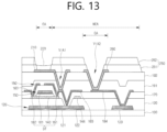
- FIGS. 12 to 16 show a manufacturing method of the display device according to an embodiment of the present disclosure
- first and the second, etc. can be used to describe various components, the components are not limited by the terms mentioned above. The terms are used only for distinguishing between one component and other components.
- first component can be designated as the second component without departing from the scope of rights of various embodiments.
- second component can be designated as the first component.
- An expression of a singular form includes the expression of plural form thereof unless otherwise explicitly mentioned in the context.
- FIG. 1 is a block diagram showing a configuration of a display device according to an embodiment of the present disclosure.
- a display device 1 includes a timing controller 10 , a gate driver 20 , a data driver 30 , a power supply unit 40 , and a display panel 50 .
- the timing controller 10 can receive an image signal RGB and a control signal CS from the outside (e.g., from a host system).
- the image signal RGB can include a plurality of grayscale data.
- the control signal CS can include, for example, a horizontal synchronization signal, a vertical synchronization signal, and a main clock signal.
- the timing controller 10 can process the image signal RGB and the control signal CS in conformity with operation conditions of the display panel 50 , and then can generate and output an image data DATA, a gate driving control signal CONT 1 , a data driving control signal CONT 2 , a power supply control signal CONT 3 .
- the gate driver 20 can generate gate signals based on the gate driving control signal CONT 1 output from the timing controller 10 .
- the gate driver 20 can provide the generated gate signals to pixels PX through a plurality of first gate lines GL 11 to GL 1 n , where n is a positive integer.
- the gate driver 20 can provide sensing signals to the pixels PX through a plurality of second gate lines GL 21 to GL 2 n .
- the sensing signal can be provided to measure characteristics of a driving transistor and/or a light emitting device provided within the pixels PX.
- the data driver 30 can generate data signals based on the image data DATA and the data driving control signal CONT 2 output from the timing controller 10 .
- the data driver 30 can provide the generated data signals to the pixels PX through a plurality of data lines DL 1 to DLm, where m is a positive integer.
- the data driver 30 can provide a reference voltage (or a sensing voltage, an initialization voltage) to the pixels PX through a plurality of sensing lines SL 1 to SLm or can sense the state of the pixels PX based on electrical signals fed back from the pixels PX.
- a reference voltage or a sensing voltage, an initialization voltage
- the power supply unit 40 can generate a driving voltage which is to be supplied to the display panel 50 based on the power supply control signal CONT 3 .
- the driving voltage can include, for example, a high potential driving voltage ELVDD and a low potential driving voltage ELVSS.
- the power supply unit 40 can supply the generated driving voltages ELVDD and ELVSS to the pixels PX through corresponding power lines PL 1 and PL 2 .
- a plurality of the pixels PX are disposed on the display panel 50 .
- the pixels PX can be arranged, for example, in a matrix form on the display panel 50 .
- the pixels PX can emit light with a luminance which corresponds to the gate signal and the data signal provided through the first gate lines GL 11 to GL 1 n and the data lines DL 1 to DLm.
- each pixel PX can represent any one of red, green, blue, and white colors. However, the embodiment is not limited thereto.
- the timing controller 10 , the gate driver 20 , the data driver 30 , and the power supply unit 40 can be each composed of a separate integrated circuit (IC), or can be configured as an IC in which at least some of them are integrated.
- IC integrated circuit
- at least one of the data driver 30 and the power supply unit 40 can be configured as an integrated circuit integrated with the timing controller 10 .
- the gate driver 20 and the data driver 30 are shown in FIG. 1 as separate components from the display panel 50 , at least one of the gate driver 20 and the data driver 30 can be implemented in an in-panel method where it is formed integrally with the display panel 50 .
- the gate driving part 20 can be formed integrally with the display panel 50 in a gate-in-panel (GIP) method.
- GIP gate-in-panel
- FIG. 2 is a circuit diagram showing an embodiment of a pixel shown in FIG. 1 .
- FIG. 2 shows the pixel PXij connected to the first i-th gate line GL 1 i and the j-th data line DLj as an example, wherein i and j are positive integers.
- the pixel PX includes a switching transistor ST, a driving transistor DT, a sensing transistor SST, a storage capacitor Cst, and a light emitting device LD (e.g., an OLED).
- a switching transistor ST a driving transistor DT
- a sensing transistor SST a sensing transistor SST
- a storage capacitor Cst a storage capacitor Cst
- a light emitting device LD e.g., an OLED
- a first electrode of the switching transistor ST is electrically connected to the j-th data line DLj, and a second electrode of the switching transistor ST is connected to a first node N 1 .
- a gate electrode of the switching transistor ST is connected to the first gate line GL 1 i .
- the switching transistor ST is turned on when a gate signal of a gate-on level is applied to the first gate line GL 1 i , and transmits the data signal applied to the data line DLj to the first node N 1 .
- a first electrode of the storage capacitor Cst can be connected to the first node N 1 , and a second electrode of the storage capacitor Cst can be configured to receive the high potential driving voltage ELVDD.
- the storage capacitor Cst can be charged with a voltage corresponding to a difference between a voltage applied to the first node N 1 and the high potential driving voltage ELVDD.
- a first electrode of the driving transistor DT is configured to receive the high potential driving voltage ELVDD, and a second electrode of the driving transistor DT is connected to a first electrode (e.g., anode electrode) of the light emitting device LD.
- a gate electrode of the driving transistor DT is electrically connected to the first node N 1 .
- the driving transistor DT can be turned on when a gate-on level voltage is applied through the first node N 1 , and can control the amount of driving current flowing through the light emitting device LD in response to the voltage applied to the gate electrode, that is, the voltage stored in the storage capacitor Cst.
- a first electrode of the sensing transistor SST is connected to the sensing line SLj, and a second electrode of the sensing transistor SST is connected to the first electrode of the light emitting device LD.
- a gate electrode of the sensing transistor SST is connected to the second gate line GL 2 i .
- the sensing transistor SST is turned on when a sensing signal of a gate-on level is applied to the second gate line GL 2 i , and transmits a reference voltage applied to the sensing line SLj to the first electrode of the light emitting device LD.
- the light emitting device LD outputs light corresponding to the driving current.
- the light emitting device LD can be an organic light emitting diode (OLED) or a micro inorganic light emitting diode having a size in a range from micro scale to nano scale.
- OLED organic light emitting diode
- micro inorganic light emitting diode having a size in a range from micro scale to nano scale.
- the present invention is not limited thereto.
- embodiments in which the light emitting device LD is composed of the organic light emitting diode will be described.
- the structure of the pixels PX is not limited to what is shown in FIG. 2 .
- the pixels PX can further include at least one element for compensating a threshold voltage of the driving transistor DT or initializing the voltage of the gate electrode of the driving transistor DT and/or the voltage of the anode electrode of the light emitting device LD.
- FIG. 2 shows an example in which the switching transistor ST, the driving transistor DT, and the sensing transistor SST are NMOS transistors.
- the present invention is not limited thereto.
- the transistors constituting each pixel PX can be composed of a PMOS transistor.
- each of the switching transistor ST, the driving transistor DT, and the sensing transistor SST can be implemented with a low temperature poly silicon (LTPS) thin film transistor, an oxide thin film transistor, or a low temperature polycrystalline oxide (LTPO) thin film transistor.
- LTPS low temperature poly silicon
- LTPO low temperature polycrystalline oxide
- FIG. 3 is a plan view of the display panel according to an embodiment of the present disclosure.
- FIG. 4 is a schematic cross sectional view taken along line I-I′ of FIG. 3 .
- a plurality of the pixels PX are disposed on the display panel 50 according to the embodiment.
- the pixels PX can represent any one of red, green, and blue colors respectively.
- three pixels PX representing red R, green G, and blue B colors can constitute one unit pixel.
- a bank 250 is arranged around each of the pixels PX.
- the bank 250 can have a structure in which a hydrophilic bank 251 and a hydrophobic bank 252 are stacked.
- the hydrophilic bank 251 extends between pixel rows and between pixel columns in a row direction X and in a column direction Y.
- the hydrophilic bank 251 is formed in the form of a grid and separates the pixels PX.
- the hydrophilic bank 251 is made of a hydrophilic inorganic insulating material, such as silicon oxide SiO2 or nitride oxide SiNx, so that a solution spreads well in the formation of a light emitting layer 220 (e.g., a solution can be attracted to or pulled into and around the hydrophilic bank 251 areas), which will be described later.
- the hydrophobic bank 252 can be formed in a partial region on the hydrophilic bank 251 .
- the hydrophobic bank 252 can be disposed between the pixel rows and can partition the pixel rows.
- the hydrophobic bank 252 is formed such that at least one region, for example, an upper region, has hydrophobicity, thereby preventing color mixing between the pixel rows.
- the pixels PX can be connected, through a contact hole formed in an auxiliary electrode contact part CA, to the second power line PL 2 to which the low potential driving voltage ELVSS is applied.
- FIG. 3 shows an example in which one auxiliary electrode contact part CA is provided in a unit pixel.
- the present embodiment is not limited thereto, and each of the pixels PX can include the auxiliary electrode contact part CA.
- the display panel 50 includes a substrate 100 , a circuit element layer formed on the substrate 100 and provided with at least one circuit element, and a light emitting device layer including the light emitting device LD.
- the substrate 100 is a base material of the display panel 50 and can be a light-transmitting substrate.
- the substrate 100 can be a rigid substrate including glass or tempered glass or a flexible substrate made of plastic.
- the substrate 100 can include a light emitting area EA and a non-light emitting area NEA.
- the non-light emitting area NEA includes the auxiliary electrode contact part CA in which contact is made between an auxiliary electrode 260 and a cathode electrode 230 of the light emitting device LD (e.g., a region where auxiliary electrode 260 directly touches cathode electrode 230 ).
- the circuit element layer is formed on the substrate 100 and can include circuit elements (e.g., transistors, capacitors, etc.) and wirings which constitute the pixel PX.
- circuit elements e.g., transistors, capacitors, etc.
- a first conductive layer 120 can be disposed on the substrate 100 .
- the first conductive layer 120 can include a light shielding layer 121 , a lower electrode 122 of the storage capacitor Cst, and an auxiliary wiring 123 .
- the auxiliary wiring 123 can be connected to the second power line PL 2 to which the low potential driving voltage ELVSS is applied.
- the light shielding layer 121 is disposed to overlap with an active layer 140 , in particular, a channel on a plane, thereby protecting an oxide semiconductor device from external light.
- the lower electrode 122 of the storage capacitor Cst can be integrally formed with the light shielding layer 121 as one pattern. However, the present embodiment is not limited thereto.
- a buffer layer 130 is disposed on the substrate 100 to cover the first conductive layer 120 .
- the buffer layer 130 can prevent diffusion of ions or impurities from the substrate 100 and block moisture penetration.
- the active layer 140 can be formed on the buffer layer 130 .
- the active layer 140 can be formed of a silicon-based semiconductor material or an oxide-based semiconductor material.
- the active layer 140 can include a source region and a drain region which include p-type or n-type impurities, and a channel formed between the source region and the drain region.
- One region of the active layer 140 can form an intermediate electrode 144 of the storage capacitor Cst.
- the intermediate electrode 144 can be disposed such that at least one region thereof overlaps with the lower electrode 122 .
- a gate insulating layer 150 can be disposed to correspond to a region where a below-described gate electrode 161 is to be formed.
- the gate insulating layer 150 can be formed on the channel of the active layer 140 .
- a second conductive layer 160 can be disposed on the gate insulating layer 150 .
- the second conductive layer 160 can include the gate electrode 161 .
- the gate electrode 161 can be disposed at a position corresponding to the channel of the active layer 140 .
- An interlayer insulating layer 170 can be formed on the second conductive layer 160 .
- a third conductive layer 180 can be formed on the interlayer insulating layer 170 .
- the third conductive layer 180 can include a source electrode 181 and a drain electrode 182 .
- the source electrode 181 and the drain electrode 182 can be connected to the source region and the drain region of the active layer 140 respectively through a contact hole which passes through the interlayer insulating layer 170 .
- the source electrode 181 and the drain electrode 182 can be formed as a single layer or multiple layers.
- the source electrode 181 , the drain electrode 182 , the gate electrode 161 , and the active layer 140 corresponding to them can constitute a transistor.
- the driving transistor DT in which the source electrode 181 is connected to the anode electrode 210 of the light emitting device LD is shown as an example.
- the third conductive layer 180 can further include an upper electrode 183 of the storage capacitor Cst.
- the upper electrode 183 can be integrally formed with the drain electrode 182 of the driving transistor DT.
- An electric field can be formed between the intermediate electrode 144 formed in the active layer 140 and the upper electrode 183 formed in the third conductive layer 180 and can function as the storage capacitor Cst.
- the third conductive layer 180 can further include a bridge electrode 184 .
- the bridge electrode 184 is connected to the auxiliary wiring 123 through a contact hole which passes through the interlayer insulating layer 170 and the buffer layer 130 .
- the circuit element layer can be covered by a passivation layer 191 and an overcoat layer 192 .
- the passivation layer 191 can be an insulating layer to protect the devices thereunder, and the overcoat layer 192 can be a planarization layer for reducing a step difference in the structure thereunder.
- the light emitting device layer is formed on the overcoat layer 192 and includes the light emitting devices LDs.
- the light emitting device LD includes the anode electrode 210 , the light emitting layer 220 , and the cathode electrode 230 .
- the anode electrode 210 is formed on the overcoat layer 192 .
- the anode electrode 210 is connected to the driving transistor DT through a first via hole VIA 1 , which passes through the overcoat layer 192 and the passivation layer 191 .
- the anode electrode 210 can be formed of a transparent conductive material such as indium tin oxide (ITO), indium zinc oxide (IZO), zinc oxide (ZnO), etc.
- the anode electrode 210 is a reflective electrode
- the anode electrode 210 can be formed as a triple layer composed of a transparent conductive layer/a reflective layer (a metal oxide layer)/a transparent conductive layer.
- the anode electrode 210 can be formed as a triple layer including ITO/Ag/ITO.
- the auxiliary electrode 260 for electrically connecting the cathode electrode 230 and the second power line PL 2 is further formed on the overcoat layer 192 .
- the auxiliary electrode 260 can be disposed in the auxiliary electrode contact part CA of the non-light emitting area NEA, can be made of the same material as the anode electrode 210 , and can be formed in the same process.
- the auxiliary electrode 260 can be connected to the bridge electrode 184 through a second via hole VIA 2 , which passes through the overcoat layer 192 and the passivation layer 191 .
- the bank 250 can be formed on the overcoat layer 192 .
- the bank 250 can be formed to expose some regions of the anode electrode 210 , for example, a central region and to cover the remaining region, for example, edges of the anode electrode 210 .
- the exposed region of the anode electrode 210 which is not covered by the bank 250 , can be defined as the light emitting area EA of the pixel PX.
- the bank 250 can be formed to expose a region of the auxiliary electrode 260 .
- the light emitting layer 220 is formed on the exposed region of the anode electrode 210 surrounded by the bank 250 .
- the light emitting layer 220 can be formed through a solution process.
- a solution for forming the light emitting layer 220 within the light emitting area EA can be applied.
- the solution can be manufactured by mixing organic materials constituting the light emitting layer 220 with a solvent.
- the solution can be jetted to the light emitting area through an inkjet apparatus having a nozzle mounted on an inkjet head.
- the applied ink is dried to form the light emitting layer 220 .
- the surface of the central region can be lower than the surface of the edge region.
- the embodiment is not limited thereto.
- a hole transport layer HTL
- HIL hole injection layer
- the cathode electrode 230 is formed on the light emitting layer 220 .
- the cathode electrode 230 can be formed of a transparent conductive material (TCO) or a semi-transmissive conductive material which is capable of transmitting light.
- An electron transport layer (ETL) 240 can be disposed between the cathode electrode 230 and the light emitting layer 220 .
- the electron transport layer 240 serves to smoothly transfer electrons injected from the cathode electrode 230 to the light emitting layer 220 .
- the electron transport layer 240 and the cathode electrode 230 can be widely formed on the display panel 50 .
- the electron transport layer 240 and the cathode electrode 230 can be sequentially stacked on the anode electrode 210 and the light emitting layer 220 .
- the electron transport layer 240 and the cathode electrode 230 can be sequentially stacked on the auxiliary electrode 260 .
- the cathode electrode 230 can be electrically connected to the second power line PL 2 via the auxiliary electrode 260 , the bridge electrode 184 , and the auxiliary wiring 123 .
- An encapsulation layer 300 can be formed on the cathode electrode 230 .
- the encapsulation layer 300 serves to prevent external moisture from penetrating into the light emitting layer 220 .
- the encapsulation layer 300 can be formed of an inorganic insulating material or can have a structure in which an inorganic insulating material and an organic insulating material are alternately stacked, and is not limited thereto.
- an electrical resistance between the cathode electrode 230 and the auxiliary electrode 260 can increase.
- a reflow process of irradiating a laser to the auxiliary electrode contact part CA can be applied.
- the electron transport layer 240 interposed between the cathode electrode 230 and the auxiliary electrode 260 is removed or at least thinned in the auxiliary electrode contact part CA, so that the electrical resistance between the cathode electrode 230 and the auxiliary electrode 260 is reduced (e.g., to improve the electrical connection between the cathode electrode and the auxiliary electrode at the CA region).
- This reflow process can be performed by irradiating a laser to the auxiliary electrode contact part CA.
- a laser is irradiated, a portion of the electron transport layer 240 can be melted and removed or thinned in at least one region on the auxiliary electrode 260 . Then, the cathode electrode 230 and the auxiliary electrode 260 can be in direct contact with each other or the electrical resistance between the cathode electrode 230 and the auxiliary electrode 260 can be reduced.
- the intensity of the laser irradiated to the auxiliary electrode contact part CA can vary depending on the region. This can cause excessive reflow of the organic layer, that is, the electron transport layer 240 in a specific region, or can cause a problem that the electron transport layer 240 is not melted in another specific region. Then, the auxiliary electrode contact part CA cannot be manufactured in a required shape, which can cause a defect of the display panel 50 .
- a defect problem of the auxiliary electrode contact part CA is solved by laser intensity imbalance due to the patterning of the auxiliary electrode 260 in a special shape.
- various patterns of the auxiliary electrode 260 will be described in more detail with reference to the drawings.
- FIG. 5 is an enlarged cross sectional view of an area AA (AAa) of FIG. 4 according to a first embodiment.
- FIG. 6 is a view showing an intensity distribution of laser irradiated to the display panel.
- FIG. 7 is a view showing a state after a reflow process of an auxiliary electrode contact part shown in FIG. 5 .
- an auxiliary electrode 260 a includes a concave portion P 1 formed on the top surface (e.g., the upper surface of auxiliary electrode 260 a can be formed from the same material as the anode electrode 210 ).
- the concave portion P 1 can be formed on the entire or a portion of exposed top surface of the auxiliary electrode 260 a.
- the concave portion P 1 can be formed as a curved surface as shown, and the present embodiment is not limited thereto. That is to say, in various embodiments, as long as a thickness of a central region of the concave portion P 1 is less than a thickness of an edge region of the concave portion P 1 and a height of the top surface in the central region is less than that of the edge region, the concave portion P 1 can have various shapes without limitation.
- the laser applied to the display panel 50 generally has an intensity distribution shown in FIG. 6 . That is, the laser can have the highest intensity in the center region and the lowest intensity in the edge region.
- the auxiliary electrode 260 a When the laser is irradiated to the auxiliary electrode contact part CA for the reflow process, the less the thickness of the auxiliary electrode 260 a is, the more easily the energy of the laser can reach the electron transport layer. Accordingly, on the region of the auxiliary electrode 260 a , which has a smaller thickness, more electron transport layers 240 can be melted.
- the electron transport layers 240 when the reflow process is performed by irradiating the laser, the electron transport layers 240 can be melted by a greater degree within the concave portion P 1 , and may not be melted or less melted in the region around the concave portion P 1 .
- the electron transport layer 240 melted within the concave portion P 1 can flow into the central region of the concave portion P 1 due to the inclination of the inner wall of the concave portion P 1 (e.g., a melted portion of electron transport layer 240 can pool together at a center of the concave portion P 1 , allowing for between contact between the cathode electrode 230 and the auxiliary electrode 260 a ).
- the electron transport layer 240 is formed on the central region of the concave portion P 1 on the auxiliary electrode 260 a .
- the electron transport layer 240 can be further formed in the region around the concave portion P 1 where the concave portion P 1 is not formed.
- the edge region of the concave portion P 1 of the auxiliary electrode 260 a is not covered by the electron transport layer 240 and is exposed upward.
- the cathode electrode 230 can be formed on the exposed region of the auxiliary electrode 260 a . Then, the cathode electrode 230 is in direct contact with the auxiliary electrode 260 a in the exposed region of the auxiliary electrode 260 a (e.g., improving the contact between the auxiliary electrode 260 a and the cathode electrode 230 ).
- the reflow of the electron transport layer 240 can be controlled, such that the electron transport layer 240 is melted in a specific region due to the concave portion P 1 of the auxiliary electrode 260 a . Accordingly, defects of the auxiliary electrode contact part CA due to excessive reflow of the electron transport layer 240 can be minimized.
- FIG. 8 is an enlarged cross sectional view of the area AA (AAc) of FIG. 4 according to a second embodiment.
- an auxiliary electrode 260 b includes a concave portion P 2 formed on the bottom surface.
- the concave portion P 2 can be formed as a curved surface as shown, and the present embodiment is not limited thereto. That is to say, in various embodiments, as long as a thickness of a central region of the concave portion P 2 is less than a thickness of an edge region of the concave portion P 2 and a height of the bottom surface in the central region is greater than that of the edge region, the concave portion P 2 can have various shapes without limitation.
- the electron transport layer 240 can be melted even further in the central region of the auxiliary electrode 260 b , which has a smaller thickness, and may not be melted or less melted in the edge region of the auxiliary electrode 260 b , which has a larger thickness.
- the melted electron transport layer 240 can flow to the edge region by peripheral tension.
- the electron transport layer 240 can be formed on the edge region of the auxiliary electrode 260 b.
- the central region of the auxiliary electrode 260 b which overlaps with the concave portion P 2 , is not covered by the electron transport layer 240 and is exposed upward.
- the cathode electrode 230 can be formed on the exposed region of the auxiliary electrode 260 b . Then, the cathode electrode 230 is in direct contact with the auxiliary electrode 260 b in the exposed region of the auxiliary electrode 260 b.
- FIG. 9 is an enlarged cross sectional view of the area AA (AAd) of FIG. 4 according to a third embodiment.
- an auxiliary electrode 260 c can include a convex portion P 3 formed on the top surface (e.g., the auxiliary electrode 260 c can have an embossed pattern, a mound or a bump in the CA region).
- the convex portion P 3 can be formed on the entire or a portion of exposed top surface of the auxiliary electrode 260 c.
- the convex portion P 3 can be formed as a curved surface as shown, and the present embodiment is not limited thereto. That is, in various embodiments, as long as a thickness of a central region of the convex portion P 3 is larger than a thickness of an edge region of the convex portion P 3 and a height of the top surface in the central region is greater than that of the edge region, the convex portion P 3 can have various shapes without limitation.
- the electron transport layer 240 can be melted.
- the melted electron transport layer 240 can flow to an edge region having a low height of the top surface.
- the edge region can include a region around the convex portion P 3 where the convex portion P 3 is not formed and/or the edge region of the convex portion P 3 .
- the electron transport layer 240 can be formed on the edge region of the auxiliary electrode 260 c.
- the central region of the convex portion P 3 is not covered by the electron transport layer 240 and is exposed upward.
- the cathode electrode 230 can be formed on the exposed region of the auxiliary electrode 260 c . Then, the cathode electrode 230 is in direct contact with the auxiliary electrode 260 c in the exposed region of the auxiliary electrode 260 c.
- FIG. 10 is an enlarged cross sectional view of the area AA (AAe) of FIG. 4 according to a fourth embodiment.
- an auxiliary electrode 260 d can include a convex portion P 4 formed on the bottom surface.
- the convex portion P 4 can be formed as a curved surface as shown, and the present embodiment is not limited thereto. That is, in various embodiments, as long as a thickness of a central region of the convex portion P 4 is larger than a thickness of an edge region of the convex portion P 4 and a height of the bottom surface in the central region is greater than that of the edge region, the convex portion P 4 can have various shapes without limitation.
- the electron transport layer 240 can be further melted in the edge region of the auxiliary electrode 260 d , which has a smaller thickness, and may not be melted or less melted in the central region of the auxiliary electrode 260 d , which has a larger thickness.
- the melted electron transport layer 240 can flow into the central region by peripheral tension.
- the electron transport layer 240 can be formed on the central region of the auxiliary electrode 260 d.
- the edge region of the auxiliary electrode 260 d which does not overlap the convex portion P 4 , is not covered by the electron transport layer 240 and is exposed upward.
- the cathode electrode 230 can be formed on the exposed region of the auxiliary electrode 260 d . Then, the cathode electrode 230 is in direct contact with the auxiliary electrode 260 d in the exposed region of the auxiliary electrode 260 d.
- FIG. 11 is an enlarged cross sectional view of the area AA (AAf) of FIG. 4 according to a fifth embodiment.
- an auxiliary electrode 260 e includes a first convex portion P 5 which is formed on the top surface and a second convex portion P 6 which is formed on the bottom surface and is disposed to overlap the first convex portion P 5 .
- the first convex portion P 5 and the second convex portion P 6 can be formed as a curved surface as shown, and the present embodiment is not limited thereto.
- the electron transport layer 240 can be melted.
- the melted electron transport layer 240 can flow to an edge region having a low height of the top surface.
- the edge region can include a region around the first convex portion P 5 where the first convex portion P 5 is not formed and/or the edge region of the first convex portion P 5 .
- the electron transport layer 240 can be formed on the edge region of the auxiliary electrode 260 e.
- the central region of the first convex portion P 5 is not covered by the electron transport layer 240 and is exposed upward.
- the cathode electrode 230 can be formed on the exposed region of the auxiliary electrode 260 e . Then, the cathode electrode 230 is in direct contact with the auxiliary electrode 260 e in the exposed region of the auxiliary electrode 260 e.
- FIGS. 12 to 16 shows a manufacturing method of the display device according to the embodiment.
- the circuit element layer can be formed on the substrate 100 .
- the first to third conductive layers 120 to 180 , the passivation layer 191 , and the overcoat layer 192 are formed on the substrate 100 .
- the anode electrode 210 is formed on the overcoat layer 192 in the light emitting area EA. Also, the auxiliary electrode 260 is formed on the overcoat layer 192 in the auxiliary electrode contact part CA of the non-light emitting area NEA. The auxiliary electrode 260 is connected to the bridge electrode 184 .
- the auxiliary electrode 260 can be formed to have a specific pattern, as described with reference to FIGS. 5 to 11 .
- the auxiliary electrode 260 can be formed to have a concave portion or a convex portion formed on the top surface and/or the bottom surface.
- the bank 250 is formed on the overcoat layer 192 .
- the bank 250 can be formed to expose the central region of the anode electrode 210 and to cover the edge region. Also, the bank 250 can be formed to expose the central region of the auxiliary electrode 260 and to cover the edge region.
- At least a portion of the surface of the bank 250 can be formed to have hydrophobicity.
- the bank 250 can be formed by applying a solution in which a hydrophobic material, such as fluorine (F) is mixed with an organic insulating material and then by a photolithography process.
- the hydrophobic material, such as fluorine can move to the top of the bank 250 by light irradiated during the photolithography process, and accordingly, the top surface of the bank 250 can have a hydrophobic property and the remaining portion can have a hydrophilic property.
- the hydrophobic bank 250 can serve as a dam to prevent ink from being mixed between the light emitting areas EA.
- the light emitting layer 220 is formed.
- the light emitting layer 220 is formed on the anode electrode 210 in the light emitting area EA defined by the bank 250 .
- the light emitting layer 220 can be formed through a solution process.
- a solution for forming the light emitting layer 220 within the light emitting area EA can be applied.
- the solution can be manufactured by mixing organic materials constituting the light emitting layer 220 with a solvent.
- the solution can be jetted to the light emitting area through an inkjet apparatus having a nozzle mounted on an inkjet head.
- the applied ink is dried to form the light emitting layer 220 .
- the surface of the central region can be lower than the surface of the edge region.
- the embodiment is not limited thereto.
- the organic layer can be the electron transport layer 240 .
- the cathode electrode 230 is formed on the electron transport layer 240 .
- the electron transport layer 240 and the cathode electrode 230 can be widely formed on the display panel 50 to cover the bank 250 and the auxiliary electrode 260 .
- the electron transport layer 240 and the cathode electrode 230 can be formed by an evaporation deposition method such as thermal deposition or by a physical vapor deposition method such as a sputtering method
- the reflow process for the electron transport layer 240 can be performed (e.g., the electron transport layer 240 can be melted away at a specific spot to improve contact between the cathode electrode 230 and the auxiliary electrode 260 , in the CA region).
- a laser can be irradiated from below (or from above) the display panel 50 .
- energy by the laser can be transferred to the electron transport layer 240 through the auxiliary electrode 260 .
- the laser irradiated to the electron transport layer 240 can have the intensity distribution shown in FIG. 6 .
- more or less energy by the laser can be transferred to a specific region of the electron transport layer 240 in accordance with the thickness and shape of the patterned auxiliary electrode 260 .
- At least a portion of the electron transport layer 240 is melted by the energy of the laser transmitted through the auxiliary electrode 260 . Then, as described with reference to FIGS. 7 to 11 , the electron transport layer 240 flows, so that at least one region of the auxiliary electrode 260 can be exposed toward the cathode electrode 230 .
- the auxiliary electrode 260 can be in direct contact with the cathode electrode 230 in the exposed region where the electron transport layer 240 is not formed.
- the electron transport layer 240 can be controlled to be selectively removed in an area on the auxiliary electrode 260 by the patterning of the auxiliary electrode 260 . Then, the auxiliary electrode 260 and the cathode electrode 230 are partially in direct contact with each other, so that an electrical connection between the cathode electrode 230 and the auxiliary electrode 260 can be stably formed.
- the cathode electrode 230 can be stably connected to the second power line PL 2 via the auxiliary electrode 260 .
- the display device and the manufacturing method thereof according to the embodiments of the present disclosure can improve a bonding force between the cathode electrode and the auxiliary electrode in consideration of the intensity distribution of laser during a reflow process.
- the display device and the manufacturing method thereof according to the embodiments of the present disclosure can optimize, through the patterned auxiliary electrode, the degree of melting of an organic layer (e.g., an electron transport layer) during the reflow process as required.
- an organic layer e.g., an electron transport layer
- the display device and the manufacturing method thereof according to the embodiments of the present disclosure can simplify the reflow process and reduce equipment cost by compensating for the limitations of laser equipment by changing the shape of the auxiliary electrode.
Landscapes
- Engineering & Computer Science (AREA)
- Microelectronics & Electronic Packaging (AREA)
- Physics & Mathematics (AREA)
- Optics & Photonics (AREA)
- Manufacturing & Machinery (AREA)
- Electroluminescent Light Sources (AREA)
- Devices For Indicating Variable Information By Combining Individual Elements (AREA)
Abstract
Description
Claims (11)
Applications Claiming Priority (2)
| Application Number | Priority Date | Filing Date | Title |
|---|---|---|---|
| KR10-2020-0189446 | 2020-12-31 | ||
| KR1020200189446A KR102848726B1 (en) | 2020-12-31 | 2020-12-31 | Display device and manufacturing method thereof |
Publications (2)
| Publication Number | Publication Date |
|---|---|
| US20220209173A1 US20220209173A1 (en) | 2022-06-30 |
| US11991893B2 true US11991893B2 (en) | 2024-05-21 |
Family
ID=82117829
Family Applications (1)
| Application Number | Title | Priority Date | Filing Date |
|---|---|---|---|
| US17/532,861 Active 2042-04-22 US11991893B2 (en) | 2020-12-31 | 2021-11-22 | Display device having an auxiliary electrode including a concave portion or a convex portion |
Country Status (2)
| Country | Link |
|---|---|
| US (1) | US11991893B2 (en) |
| KR (1) | KR102848726B1 (en) |
Families Citing this family (2)
| Publication number | Priority date | Publication date | Assignee | Title |
|---|---|---|---|---|
| KR20240057896A (en) * | 2022-10-25 | 2024-05-03 | 엘지디스플레이 주식회사 | Light emitting display device |
| KR20250109258A (en) * | 2024-01-09 | 2025-07-17 | 삼성디스플레이 주식회사 | Display device |
Citations (5)
| Publication number | Priority date | Publication date | Assignee | Title |
|---|---|---|---|---|
| US20110241563A1 (en) * | 2010-04-05 | 2011-10-06 | Samsung Mobile Display Co., Ltd. | Organic light emitting diode display |
| US20130256638A1 (en) * | 2012-03-27 | 2013-10-03 | Sony Corporation | Display device and method of manufacturing the same, method of repairing display device, and electronic apparatus |
| KR101768956B1 (en) | 2016-07-29 | 2017-08-18 | 엘지디스플레이 주식회사 | Organic Light Emitting Diode Device AND Method for Manufacturing thereof |
| US20180254429A1 (en) * | 2016-06-30 | 2018-09-06 | Lg Display Co., Ltd. | Organic light-emitting display device and method of fabricating the same |
| KR102113616B1 (en) | 2013-06-28 | 2020-06-05 | 엘지디스플레이 주식회사 | Organic light emitting display device and manufacturing method of the same |
Family Cites Families (5)
| Publication number | Priority date | Publication date | Assignee | Title |
|---|---|---|---|---|
| KR102624878B1 (en) * | 2016-06-30 | 2024-01-16 | 엘지디스플레이 주식회사 | Organic light emitting display device and method for manufacturing the same |
| KR101878186B1 (en) * | 2016-07-29 | 2018-08-17 | 엘지디스플레이 주식회사 | Organic light emitting display and fabricating method thereof |
| KR102854033B1 (en) * | 2016-11-30 | 2025-09-02 | 엘지디스플레이 주식회사 | Organic light emitting diode display device |
| WO2019079648A1 (en) * | 2017-10-19 | 2019-04-25 | Tunnel Radio Of America, Inc. | Aerial radio-frequency identification (rfid) tracking and data collection system |
| KR102532308B1 (en) * | 2018-07-26 | 2023-05-15 | 삼성디스플레이 주식회사 | Display device |
-
2020
- 2020-12-31 KR KR1020200189446A patent/KR102848726B1/en active Active
-
2021
- 2021-11-22 US US17/532,861 patent/US11991893B2/en active Active
Patent Citations (5)
| Publication number | Priority date | Publication date | Assignee | Title |
|---|---|---|---|---|
| US20110241563A1 (en) * | 2010-04-05 | 2011-10-06 | Samsung Mobile Display Co., Ltd. | Organic light emitting diode display |
| US20130256638A1 (en) * | 2012-03-27 | 2013-10-03 | Sony Corporation | Display device and method of manufacturing the same, method of repairing display device, and electronic apparatus |
| KR102113616B1 (en) | 2013-06-28 | 2020-06-05 | 엘지디스플레이 주식회사 | Organic light emitting display device and manufacturing method of the same |
| US20180254429A1 (en) * | 2016-06-30 | 2018-09-06 | Lg Display Co., Ltd. | Organic light-emitting display device and method of fabricating the same |
| KR101768956B1 (en) | 2016-07-29 | 2017-08-18 | 엘지디스플레이 주식회사 | Organic Light Emitting Diode Device AND Method for Manufacturing thereof |
Also Published As
| Publication number | Publication date |
|---|---|
| US20220209173A1 (en) | 2022-06-30 |
| KR102848726B1 (en) | 2025-08-22 |
| KR20220096738A (en) | 2022-07-07 |
Similar Documents
| Publication | Publication Date | Title |
|---|---|---|
| US11574985B2 (en) | Organic light-emitting diode display device and method of manufacturing same | |
| US20210193954A1 (en) | Display device and manufacturing method of same | |
| CN113130590A (en) | Organic light emitting diode display device including touch sensor and method of manufacturing the same | |
| US12207501B2 (en) | Transparent display panel | |
| KR101362164B1 (en) | Organcic electro-luminescence dispaly and manufacturing method thereof | |
| KR101480005B1 (en) | Organic light emitting display and manufacturing method thereof | |
| US11991893B2 (en) | Display device having an auxiliary electrode including a concave portion or a convex portion | |
| KR101258261B1 (en) | Organic Light Emitting Display Device | |
| US12317690B2 (en) | Display device and method of manufacturing same | |
| US11910634B2 (en) | Display device and manufacturing method thereof | |
| KR102745536B1 (en) | Display device | |
| JP7441290B2 (en) | Display device and its manufacturing method {DISPLAY DEVICE AND MANUFACTURING METHOD THEREOF} | |
| US12490631B2 (en) | Light emitting display device | |
| US20220208908A1 (en) | Display device and manufacturing method thereof | |
| US10923536B2 (en) | Organic el display device and method of manufacturing organic el display device | |
| CN111919510B (en) | display screen | |
| US12250846B2 (en) | Light emitting element having light emitting layer and metal layer sequentially stacked on conductive ball, manufacturing method thereof, display device including light emitting element, and manufacturing method thereof | |
| US12557523B2 (en) | Display device and manufacturing method thereof | |
| KR102874595B1 (en) | Display device and manufacturing method thereof | |
| US20250221263A1 (en) | Display device | |
| KR20220080417A (en) | Display device and manufacturing method thereof |
Legal Events
| Date | Code | Title | Description |
|---|---|---|---|
| FEPP | Fee payment procedure |
Free format text: ENTITY STATUS SET TO UNDISCOUNTED (ORIGINAL EVENT CODE: BIG.); ENTITY STATUS OF PATENT OWNER: LARGE ENTITY |
|
| AS | Assignment |
Owner name: LG DISPLAY CO., LTD., KOREA, REPUBLIC OF Free format text: ASSIGNMENT OF ASSIGNORS INTEREST;ASSIGNOR:JUNG, SUNGGOO;REEL/FRAME:058230/0134 Effective date: 20211110 |
|
| STPP | Information on status: patent application and granting procedure in general |
Free format text: DOCKETED NEW CASE - READY FOR EXAMINATION |
|
| STPP | Information on status: patent application and granting procedure in general |
Free format text: NON FINAL ACTION MAILED |
|
| STPP | Information on status: patent application and granting procedure in general |
Free format text: RESPONSE TO NON-FINAL OFFICE ACTION ENTERED AND FORWARDED TO EXAMINER |
|
| STPP | Information on status: patent application and granting procedure in general |
Free format text: NOTICE OF ALLOWANCE MAILED -- APPLICATION RECEIVED IN OFFICE OF PUBLICATIONS |
|
| STPP | Information on status: patent application and granting procedure in general |
Free format text: PUBLICATIONS -- ISSUE FEE PAYMENT VERIFIED |
|
| STCF | Information on status: patent grant |
Free format text: PATENTED CASE |