US11973009B2 - Lead frame assembly for a semiconductor device - Google Patents
Lead frame assembly for a semiconductor device Download PDFInfo
- Publication number
- US11973009B2 US11973009B2 US16/919,426 US202016919426A US11973009B2 US 11973009 B2 US11973009 B2 US 11973009B2 US 202016919426 A US202016919426 A US 202016919426A US 11973009 B2 US11973009 B2 US 11973009B2
- Authority
- US
- United States
- Prior art keywords
- lead
- die
- merged
- frame assembly
- connection portion
- Prior art date
- Legal status (The legal status is an assumption and is not a legal conclusion. Google has not performed a legal analysis and makes no representation as to the accuracy of the status listed.)
- Active
Links
Images


Classifications
-
- H01L23/49524—
-
- H—ELECTRICITY
- H10—SEMICONDUCTOR DEVICES; ELECTRIC SOLID-STATE DEVICES NOT OTHERWISE PROVIDED FOR
- H10W—GENERIC PACKAGES, INTERCONNECTIONS, CONNECTORS OR OTHER CONSTRUCTIONAL DETAILS OF DEVICES COVERED BY CLASS H10
- H10W70/00—Package substrates; Interposers; Redistribution layers [RDL]
- H10W70/40—Leadframes
- H10W70/421—Shapes or dispositions
-
- H01L23/49555—
-
- H—ELECTRICITY
- H10—SEMICONDUCTOR DEVICES; ELECTRIC SOLID-STATE DEVICES NOT OTHERWISE PROVIDED FOR
- H10W—GENERIC PACKAGES, INTERCONNECTIONS, CONNECTORS OR OTHER CONSTRUCTIONAL DETAILS OF DEVICES COVERED BY CLASS H10
- H10W70/00—Package substrates; Interposers; Redistribution layers [RDL]
- H10W70/40—Leadframes
- H10W70/421—Shapes or dispositions
- H10W70/424—Cross-sectional shapes
- H10W70/427—Bent parts
- H10W70/429—Bent parts being the outer leads
-
- H—ELECTRICITY
- H10—SEMICONDUCTOR DEVICES; ELECTRIC SOLID-STATE DEVICES NOT OTHERWISE PROVIDED FOR
- H10W—GENERIC PACKAGES, INTERCONNECTIONS, CONNECTORS OR OTHER CONSTRUCTIONAL DETAILS OF DEVICES COVERED BY CLASS H10
- H10W70/00—Package substrates; Interposers; Redistribution layers [RDL]
- H10W70/40—Leadframes
- H10W70/464—Additional interconnections in combination with leadframes
- H10W70/466—Tape carriers or flat leads
-
- H—ELECTRICITY
- H10—SEMICONDUCTOR DEVICES; ELECTRIC SOLID-STATE DEVICES NOT OTHERWISE PROVIDED FOR
- H10W—GENERIC PACKAGES, INTERCONNECTIONS, CONNECTORS OR OTHER CONSTRUCTIONAL DETAILS OF DEVICES COVERED BY CLASS H10
- H10W70/00—Package substrates; Interposers; Redistribution layers [RDL]
- H10W70/40—Leadframes
- H10W70/481—Leadframes for devices being provided for in groups H10D8/00 - H10D48/00
-
- H—ELECTRICITY
- H10—SEMICONDUCTOR DEVICES; ELECTRIC SOLID-STATE DEVICES NOT OTHERWISE PROVIDED FOR
- H10W—GENERIC PACKAGES, INTERCONNECTIONS, CONNECTORS OR OTHER CONSTRUCTIONAL DETAILS OF DEVICES COVERED BY CLASS H10
- H10W74/00—Encapsulations, e.g. protective coatings
- H10W74/10—Encapsulations, e.g. protective coatings characterised by their shape or disposition
- H10W74/111—Encapsulations, e.g. protective coatings characterised by their shape or disposition the semiconductor body being completely enclosed
-
- H—ELECTRICITY
- H10—SEMICONDUCTOR DEVICES; ELECTRIC SOLID-STATE DEVICES NOT OTHERWISE PROVIDED FOR
- H10W—GENERIC PACKAGES, INTERCONNECTIONS, CONNECTORS OR OTHER CONSTRUCTIONAL DETAILS OF DEVICES COVERED BY CLASS H10
- H10W95/00—Packaging processes not covered by the other groups of this subclass
-
- H—ELECTRICITY
- H10—SEMICONDUCTOR DEVICES; ELECTRIC SOLID-STATE DEVICES NOT OTHERWISE PROVIDED FOR
- H10W—GENERIC PACKAGES, INTERCONNECTIONS, CONNECTORS OR OTHER CONSTRUCTIONAL DETAILS OF DEVICES COVERED BY CLASS H10
- H10W72/00—Interconnections or connectors in packages
- H10W72/90—Bond pads, in general
- H10W72/921—Structures or relative sizes of bond pads
- H10W72/926—Multiple bond pads having different sizes
-
- H—ELECTRICITY
- H10—SEMICONDUCTOR DEVICES; ELECTRIC SOLID-STATE DEVICES NOT OTHERWISE PROVIDED FOR
- H10W—GENERIC PACKAGES, INTERCONNECTIONS, CONNECTORS OR OTHER CONSTRUCTIONAL DETAILS OF DEVICES COVERED BY CLASS H10
- H10W74/00—Encapsulations, e.g. protective coatings
-
- H—ELECTRICITY
- H10—SEMICONDUCTOR DEVICES; ELECTRIC SOLID-STATE DEVICES NOT OTHERWISE PROVIDED FOR
- H10W—GENERIC PACKAGES, INTERCONNECTIONS, CONNECTORS OR OTHER CONSTRUCTIONAL DETAILS OF DEVICES COVERED BY CLASS H10
- H10W90/00—Package configurations
- H10W90/701—Package configurations characterised by the relative positions of pads or connectors relative to package parts
- H10W90/751—Package configurations characterised by the relative positions of pads or connectors relative to package parts of bond wires
- H10W90/756—Package configurations characterised by the relative positions of pads or connectors relative to package parts of bond wires between a chip and a stacked lead frame, conducting package substrate or heat sink
-
- H—ELECTRICITY
- H10—SEMICONDUCTOR DEVICES; ELECTRIC SOLID-STATE DEVICES NOT OTHERWISE PROVIDED FOR
- H10W—GENERIC PACKAGES, INTERCONNECTIONS, CONNECTORS OR OTHER CONSTRUCTIONAL DETAILS OF DEVICES COVERED BY CLASS H10
- H10W90/00—Package configurations
- H10W90/701—Package configurations characterised by the relative positions of pads or connectors relative to package parts
- H10W90/761—Package configurations characterised by the relative positions of pads or connectors relative to package parts of strap connectors
- H10W90/766—Package configurations characterised by the relative positions of pads or connectors relative to package parts of strap connectors between a chip and a stacked lead frame, conducting package substrate or heat sink
Definitions
- the present disclosure relates to a lead frame assembly for a semiconductor device.
- the present disclosure relates a clip frame structure for a semiconductor device, a semiconductor device comprising the same and an associated method of manufacturing the semiconductor device.
- clip bonded packages are commonly used as lead frame arrangements to make connections from a semiconductor die to external contacts of the device.
- Clip bonded packages have a number of advantages over conventional wire bonded packages. For example, clip bonded packages are typically used for mechanically robust and reliable electrical connections to and from the semiconductor die in automotive applications.
- the conductive clip material may have increased thermal mass compared to the wire bond material and can thus act as a heat sink for the semiconductor die.
- semiconductor device 100 comprises a semiconductor die 104 mounted on a die pad 106 .
- a clip member 102 electrically connects contact terminals on a top surface of the semiconductor die 104 to external leads 108 .
- the clip member is electrically connected to and mechanically bonded to the external leads 108 using a solder connection 110 .
- This solder connection 110 results in increased connection resistance which can result in increased device resistance.
- the clip member is a source connection
- the increased resistance may result in increased drain-source on resistance, R dson .
- aspects of the present disclosure involve semiconductor devices comprising improved lead frame arrangements and a method of manufacturing such semiconductor devices.
- a lead frame assembly for a semiconductor device, the lead frame assembly comprising: a die attach structure and a clip frame structure, the clip frame structure comprising: a die connection portion configured for contacting a contact terminal on a top side of the semiconductor die; and a continuous lead portion extending along the die connection portion; wherein the continuous lead portion is integrally formed with the die connection portion.
- the continuous lead portion may be a merged lead portion which extends substantially across the width of the die connection portion.
- the continuous lead portion may be configured and arranged to maximise operating current and minimise spreading resistance of the clip frame structure.
- the continuous lead portion may comprise one or more bends therein configured and arranged to allow the lead portion to contact a carrier.
- the continuous lead portion may further comprise a plurality of lead ends.
- a semiconductor device comprising a lead frame assembly according to embodiments.
- a method of manufacturing a semiconductor device comprising: providing a lead frame assembly; mounting a semiconductor die on a die attach structure of the lead frame assembly; providing a clip frame structure, the clip frame structure comprising: a die connection portion configured to contacting a contact terminal on a top side of the semiconductor die; and a continuous lead portion extending along the die connection portion; wherein the continuous lead is portion integrally formed with the die connection portion.
- the continuous lead portion may be a merged lead portion and may be formed to extend substantially across the width of the die connection portion.
- the continuous lead portion may be configured and arranged to maximise operating current and minimise spreading resistance of the clip frame structure.
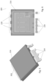
- FIG. 1 a shows a perspective view of a known lead frame arrangement.
- FIG. 1 b shows a side view of a known lead frame arrangement.
- FIG. 2 a illustrates a perspective view of a lead frame arrangement according to an embodiment.
- FIG. 2 b illustrates a side view of a lead frame arrangement according to an embodiment.
- FIG. 3 illustrates a perspective view of a lead frame arrangement according to an embodiment.
- FIG. 4 illustrates a perspective view of a clip arrangement according to an embodiment.
- FIG. 5 illustrates a perspective view of a semiconductor device according to an embodiment.
- FIG. 6 illustrates a top view of a semiconductor device according to an embodiment.
- FIGS. 7 a to 7 h illustrate the process steps for manufacturing a semiconductor device according to an embodiment.
- FIGS. 2 a and 2 b a semiconductor device 200 prior to moulding and comprising a lead frame assembly 202 according to an embodiment is illustrated in FIGS. 2 a and 2 b .
- the semiconductor device 200 generally comprises a die attach structure 204 and a clip frame structure 206 , forming the lead frame assembly 202 , and a semiconductor die 208 attached to both the die attach structure 204 and the clip frame structure 206 .
- the die attach structure 204 is typically arranged for mounting a semiconductor die 208 thereon and providing support for the clip frame structure 206 .
- the die attach structure 204 may, depending on the arrangement of contact terminals, such as source, gate or drain, of semiconductor die 208 , provide contact to a back-side or bottom contact of the semiconductor die 208 .
- the die attach structure 204 is typically formed of a metallic conductive material, such as copper. In this way the die attach structure 204 may provide a bottom external lead 203 , such as a drain contact or tab, to a back-side or bottom contact terminal arranged on the semiconductor die 208 .
- the bottom external lead 203 may extend outside of the moulded package material of the semiconductor device 200 to form a heat sink tab to the bottom of the semiconductor die 208 , as illustrated for example in FIG. 5 .
- the semiconductor die 208 is fixedly arranged on the die attach structure 204
- the clip frame structure 206 is fixedly connected to the semiconductor die 208 and the die attach structure 204 .
- the clip frame structure 206 is formed of two distinct but integrally formed parts, namely: a die connection portion 210 ; and a lead portion 212 .
- the die connection portion 210 may be generally rectangular in shape and/or may be dimensioned such that it substantially corresponds to the dimensions of a contact terminal on the top side of the semiconductor die 208 to which the die connection portion 210 is attached.
- the bottom or backside contact terminal of the semiconductor die 208 may be fixedly attached to the die attach structure 204 .
- the semiconductor die 208 may be fixedly attached to and may be electrically connected, via a bottom contact terminal (not illustrated) to the die attach structure 204 using any suitable bonding material such as a solder or a conductive adhesive.
- the die connection portion of the clip frame structure 206 is fixedly attached to the contact terminal arranged on a top side of the semiconductor die 208 , using an appropriate bonding material, such as for example, a solder or a conductive adhesive.
- the lead portion 212 is a continuous and merged section extending from the die connection portion 210 .
- the lead portion 212 is continuous in that forms a substantially elongate member extending away from and along the width of the die connection portion 210 .
- the lead portion 212 has a continuous width W and may be seen as a merged member, that is without bifurcation or plurality of finger like lead members, which extends substantially along the width of the die connection portion 210 .
- the lead portion 212 is arranged as a so-called “gull wing” lead having one or more angles or bends to allow the lead portion to contact the PCB.
- the lead portion 212 being continuous and merged may be arranged as a plate like member having the appropriate gull-wing bends formed therein.
- the lead portion 212 can be dimensioned such that it aligns or corresponds to the footprint of the contacts on a PCB (not illustrated).
- W width
- the lead portion 212 can be dimensioned such that it aligns or corresponds to the footprint of the contacts on a PCB (not illustrated).
- the lead portion By arranging the lead portion in this way it is possible to reduce the reduce the package resistance of the lead frame assembly 202 and thus reduce the operating resistance, such as Rdson, of the semiconductor device 200 .
- the above arrangement does not significantly increase the inductance of the lead frame assembly 202 .
- the resistance of the clip frame structure may be 0.34717 m ⁇ with an inductance of 1.9718 nH.
- the resistance of the clip frame structure may be 0.49792 m ⁇ with an inductance of 1.9898 nH.
- the semiconductor die 208 and the clip frame structure 206 is then encapsulated using a moulding material 216 (as illustrated for example in FIG. 5 ).
- the lead portion 212 and the bottom external lead 203 project through the mould compound 216 to allow the lead portion 212 and the bottom external lead 203 to contact an external carrier such as a PCB.
- the clip frame structure 206 is typically formed from a single unitary sheet of metal, such as copper, which is formed or stamped to produce the desired structure. In this way the thickness of the die connection portion 210 and a lead portion 212 of the clip frame structure 206 may be equal.
- the choice of metal is entirely at the choice of the skilled person and may be chosen dependent on the required electrical characteristics of the lead frame assembly for the semiconductor device 200 .
- FIGS. 3 and 4 illustrate a further embodiment of the lead frame assembly 202 .
- the arrangement of FIGS. 3 and 4 includes generally comprises a die attach structure 204 and a clip frame structure 206 , forming the lead frame assembly 202 , and a semiconductor die 208 attached to both the die attach structure 204 and the clip frame structure 206 .
- FIGS. 3 and 4 also includes a number of optional slots or holes 220 formed through the die connection portion 210 and the bottom external lead 203 .
- the slots or holes 220 act as anchor or locking points for the mould compound 216 and allow for improved adhesion or attachment of the mould compound 216 to the lead frame assembly 202 .
- Improved adhesion of mould compound prevents can reduce stress and package cracking during lead forming, that is cutting and bending of the die connection portion 210 and or the bottom external lead 203 post moulding.
- optional slots or holes 221 formed through the die connection portion 210 traverse or extend lengthways across the die connection portion 210 . This allows for both stress relief and solder protection.
- the holes or slots 221 formed in the die connection portion 210 reduce stress spreading across the surface of the die connection portion 210 as it is fixed to the terminal arranged on the top surface of the semiconductor die. In other words the holes or slots 221 distort the stress induced the die connection portion 210 so stress does not propagate across the die connection portion 210 . In terms of solder protection, the holes or slots 221 allow for gasses to escape from under the die connection portion 210 during solder reflow processes.
- Optional slots or holes 212 may also be incorporated in the lead portion 212 to prevent the leads from springing back, due to the elastic return of the metal after formation of the leads. This also makes the leads more flexible during board level temperature cycling which can prevent the solder joints of the leads to the PCB from breaking or cracking.
- FIGS. 3 , 4 and 5 also illustrate one or more optional lead end portions 224 arranged at one end of the lead portion 212 distal to the die connection portion 210 .
- the lead end portions 224 and the lead portion 212 may comprise one or more bends 230 intermediate the die connection portion 210 and an extremity of the lead end portions 224 , such that the leads are formed as so-called “gull wing” leads.
- the lead end portions 224 may be arranged in any standard lead geometry as required by the footprint of the contacts on a PCB.
- the lead geometry may be the Small Outline Integrated Circuit (SOIC) such as SO8, SO14, SO16 or any other appropriate package outline.
- SOIC Small Outline Integrated Circuit
- clip frame structure 206 may form a source connection to a source terminal on top side of the semiconductor die 208 .
- a lead 218 may form a gate connection to a gate terminal also formed on the top side of the semiconductor die 208 .
- the bottom external lead 203 may form a drain connection to a drain terminal formed on the back side of the semiconductor die 106 .
- the semiconductor die 106 may be a field effect transistor.
- the semiconductor die 208 may be a bipolar junction transistor.
- the clip frame structure 206 may form a collector connection to a collector terminal on the top side of the semiconductor die 208 .
- the lead 218 may form a base connection to a base terminal also formed on the top side of the semiconductor die 208 .
- the bottom external lead 203 may form an emitter connection to an emitter terminal formed on the back side of the semiconductor die 208 .
- FIG. 6 illustrates the slots or holes 220 arranged in the bottom external lead 203 anchoring the mould compound 216 to the bottom external lead 203 so as to allow for improved adhesion or attachment of the mould compound 216 to the bottom external lead 203 .
- FIGS. 7 a to 7 h illustrate the process flow steps for manufacturing a semiconductor device according to embodiments.
- the die attach structure 204 with a bottom external lead 203 extending therefrom is provided.
- the die attach structure 204 and bottom external lead 203 may be formed of any appropriate conductive material such as copper.
- the arrangement of FIG. 7 a shows a single die attach structure 204 , however the skilled person will appreciate that a plurality of die attach structures may be arranged in a strip or matrix.
- a die attach material 215 is dispensed onto the die attach structure 204 .
- the die attach material 215 is arranged for fixedly mounting the semiconductor die 208 to the die attach material 215 , as illustrated in FIG. 7 c .
- the die attach material 215 may be any appropriate adhesive material such as a solder or conductive adhesive.
- a contact terminal attach material is dispended on the top side contact of the semiconductor die 208 for electrical and mechanical connection of the clip frame structure 206 to the semiconductor die 208 as illustrated in FIG. 7 d .
- the die attach material may be applied by any appropriate process such as adhesive or solder printing or dispense.
- the contact terminal attach material 214 is arranged on the one or more top contacts of the semiconductor die 208 .
- the clip frame structure 206 may then be arranged on the contact terminals, as illustrated in FIG. 7 e . Whilst the arrangement of FIG. 7 e illustrates a single clip frame structure 206 arranged on the semiconductor die 208 , the skilled person will appreciate that a plurality of such clip frame structures may be arranged in a strip or matrix corresponding to the plurality of die attach structures each having a semiconductor die arranged thereon. Following connection of the clip frame structure 206 the assembly undergoes solder re-flow to solidify the die attach material and the contact terminal attach material. Following re-flow, the assembly may be packaged in a mould material 216 as illustrated in FIG. 7 f.
- the lead end portions 224 are formed by trimming the lead portion 212 and bending the leads to form the gull-wing arrangement.
- the process is completed in FIG. 7 h by trimming of the bottom external lead 203 .
Landscapes
- Lead Frames For Integrated Circuits (AREA)
- Structures Or Materials For Encapsulating Or Coating Semiconductor Devices Or Solid State Devices (AREA)
Abstract
Description
Claims (12)
Priority Applications (1)
| Application Number | Priority Date | Filing Date | Title |
|---|---|---|---|
| US18/631,535 US20240258207A1 (en) | 2019-07-03 | 2024-04-10 | Lead frame assembly for a semiconductor device |
Applications Claiming Priority (3)
| Application Number | Priority Date | Filing Date | Title |
|---|---|---|---|
| EP19184250 | 2019-07-03 | ||
| EP19184250.9 | 2019-07-03 | ||
| EP19184250.9A EP3761359B1 (en) | 2019-07-03 | 2019-07-03 | A lead frame assembly for a semiconductor device |
Related Child Applications (1)
| Application Number | Title | Priority Date | Filing Date |
|---|---|---|---|
| US18/631,535 Continuation US20240258207A1 (en) | 2019-07-03 | 2024-04-10 | Lead frame assembly for a semiconductor device |
Publications (2)
| Publication Number | Publication Date |
|---|---|
| US20210005538A1 US20210005538A1 (en) | 2021-01-07 |
| US11973009B2 true US11973009B2 (en) | 2024-04-30 |
Family
ID=67184786
Family Applications (2)
| Application Number | Title | Priority Date | Filing Date |
|---|---|---|---|
| US16/919,426 Active US11973009B2 (en) | 2019-07-03 | 2020-07-02 | Lead frame assembly for a semiconductor device |
| US18/631,535 Pending US20240258207A1 (en) | 2019-07-03 | 2024-04-10 | Lead frame assembly for a semiconductor device |
Family Applications After (1)
| Application Number | Title | Priority Date | Filing Date |
|---|---|---|---|
| US18/631,535 Pending US20240258207A1 (en) | 2019-07-03 | 2024-04-10 | Lead frame assembly for a semiconductor device |
Country Status (3)
| Country | Link |
|---|---|
| US (2) | US11973009B2 (en) |
| EP (1) | EP3761359B1 (en) |
| CN (2) | CN121568581A (en) |
Families Citing this family (7)
| Publication number | Priority date | Publication date | Assignee | Title |
|---|---|---|---|---|
| EP3996129A1 (en) * | 2020-11-04 | 2022-05-11 | Nexperia B.V. | A semiconductor device and a method of manufacturing a semiconductor device |
| CN115547841A (en) * | 2021-06-30 | 2022-12-30 | 意法半导体股份有限公司 | Method for manufacturing semiconductor device and corresponding semiconductor device |
| IT202100017207A1 (en) | 2021-06-30 | 2022-12-30 | St Microelectronics Srl | Process for manufacturing semiconductor devices and corresponding semiconductor device |
| EP4184571A1 (en) * | 2021-11-18 | 2023-05-24 | Nexperia B.V. | A semiconductor package with improved connection of the pins to the bond pads of the semiconductor die |
| CN117766498A (en) * | 2022-09-16 | 2024-03-26 | 力特半导体(无锡)有限公司 | Asymmetric Transient Voltage Suppressor Package Structure |
| US20240312855A1 (en) * | 2023-03-17 | 2024-09-19 | Semiconductor Components Industries, Llc | Full ag sinter discrete premium package |
| KR20260015929A (en) * | 2023-06-27 | 2026-02-03 | 테슬라, 인크. | Semiconductor package with directional locking structure |
Citations (14)
| Publication number | Priority date | Publication date | Assignee | Title |
|---|---|---|---|---|
| US6307755B1 (en) * | 1999-05-27 | 2001-10-23 | Richard K. Williams | Surface mount semiconductor package, die-leadframe combination and leadframe therefor and method of mounting leadframes to surfaces of semiconductor die |
| US20020140067A1 (en) * | 2001-03-29 | 2002-10-03 | Tetsuji Hori | Semiconductor package and manufacturing method thereof |
| US20040080028A1 (en) * | 2002-09-05 | 2004-04-29 | Kabushiki Kaisha Toshiba | Semiconductor device with semiconductor chip mounted in package |
| US6762067B1 (en) * | 2000-01-18 | 2004-07-13 | Fairchild Semiconductor Corporation | Method of packaging a plurality of devices utilizing a plurality of lead frames coupled together by rails |
| US20050224925A1 (en) | 2004-04-01 | 2005-10-13 | Peter Chou | Lead frame having a tilt flap for locking molding compound and semiconductor device having the same |
| US20070108564A1 (en) * | 2005-03-30 | 2007-05-17 | Wai Kwong Tang | Thermally enhanced power semiconductor package system |
| WO2007061558A2 (en) | 2005-11-18 | 2007-05-31 | Fairchild Semiconductor Corporation | Semiconductor die package using leadframe and clip and method of manufacturing |
| US20070228556A1 (en) * | 2006-03-31 | 2007-10-04 | Infineon Technologies Ag | Power Semiconductor Component with a Power Semiconductor Chip and Method for Producing the Same |
| US20090008775A1 (en) | 2007-07-05 | 2009-01-08 | Nec Electronics Corporation | Semiconductor device with welded leads and method of manufacturing the same |
| US20100109135A1 (en) * | 2008-11-06 | 2010-05-06 | Jereza Armand Vincent C | Semiconductor die package including lead with end portion |
| US20100193921A1 (en) * | 2009-02-05 | 2010-08-05 | Jereza Armand Vincent C | Semiconductor die package and method for making the same |
| US20140084433A1 (en) | 2012-09-25 | 2014-03-27 | Infineon Technologies Ag | Semiconductor Device Having a Clip Contact |
| US20140361419A1 (en) * | 2013-06-10 | 2014-12-11 | Yan Xun Xue | Power control device and preparation method thereof |
| US20190190391A1 (en) * | 2016-08-30 | 2019-06-20 | Panasonic Intellectual Property Management Co., Ltd. | Switching power supply device and semiconductor device |
Family Cites Families (16)
| Publication number | Priority date | Publication date | Assignee | Title |
|---|---|---|---|---|
| JP2635851B2 (en) * | 1991-06-19 | 1997-07-30 | ローム株式会社 | Lead frame structure used for manufacturing electronic components |
| JP2959521B2 (en) * | 1997-05-21 | 1999-10-06 | 日本電気株式会社 | Semiconductor device manufacturing method, lead frame |
| US6075286A (en) * | 1997-06-02 | 2000-06-13 | International Rectifier Corporation | Stress clip design |
| KR20000057810A (en) * | 1999-01-28 | 2000-09-25 | 가나이 쓰토무 | Semiconductor device |
| US6521982B1 (en) * | 2000-06-02 | 2003-02-18 | Amkor Technology, Inc. | Packaging high power integrated circuit devices |
| US6867481B2 (en) * | 2003-04-11 | 2005-03-15 | Fairchild Semiconductor Corporation | Lead frame structure with aperture or groove for flip chip in a leaded molded package |
| JP4450230B2 (en) * | 2005-12-26 | 2010-04-14 | 株式会社デンソー | Semiconductor device |
| US20090057852A1 (en) * | 2007-08-27 | 2009-03-05 | Madrid Ruben P | Thermally enhanced thin semiconductor package |
| US8106501B2 (en) * | 2008-12-12 | 2012-01-31 | Fairchild Semiconductor Corporation | Semiconductor die package including low stress configuration |
| JP5107839B2 (en) * | 2008-09-10 | 2012-12-26 | ルネサスエレクトロニクス株式会社 | Semiconductor device |
| US8581376B2 (en) * | 2010-03-18 | 2013-11-12 | Alpha & Omega Semiconductor Incorporated | Stacked dual chip package and method of fabrication |
| KR101249745B1 (en) * | 2011-05-16 | 2013-04-03 | 제엠제코(주) | Clip for semiconductor package, semiconductor package using the same amd method for fabricating the package |
| JP2015176871A (en) * | 2014-03-12 | 2015-10-05 | 株式会社東芝 | Semiconductor device and manufacturing method thereof |
| KR20160033870A (en) * | 2014-09-18 | 2016-03-29 | 제엠제코(주) | Semiconductor package with clip structure |
| US9818675B2 (en) * | 2015-03-31 | 2017-11-14 | Stmicroelectronics, Inc. | Semiconductor device including conductive clip with flexible leads and related methods |
| US10553524B2 (en) * | 2017-10-30 | 2020-02-04 | Microchip Technology Incorporated | Integrated circuit (IC) die attached between an offset lead frame die-attach pad and a discrete die-attach pad |
-
2019
- 2019-07-03 EP EP19184250.9A patent/EP3761359B1/en active Active
-
2020
- 2020-07-02 US US16/919,426 patent/US11973009B2/en active Active
- 2020-07-03 CN CN202511765381.7A patent/CN121568581A/en active Pending
- 2020-07-03 CN CN202010630833.1A patent/CN112185923A/en active Pending
-
2024
- 2024-04-10 US US18/631,535 patent/US20240258207A1/en active Pending
Patent Citations (15)
| Publication number | Priority date | Publication date | Assignee | Title |
|---|---|---|---|---|
| US6307755B1 (en) * | 1999-05-27 | 2001-10-23 | Richard K. Williams | Surface mount semiconductor package, die-leadframe combination and leadframe therefor and method of mounting leadframes to surfaces of semiconductor die |
| US6762067B1 (en) * | 2000-01-18 | 2004-07-13 | Fairchild Semiconductor Corporation | Method of packaging a plurality of devices utilizing a plurality of lead frames coupled together by rails |
| US20020140067A1 (en) * | 2001-03-29 | 2002-10-03 | Tetsuji Hori | Semiconductor package and manufacturing method thereof |
| US20040080028A1 (en) * | 2002-09-05 | 2004-04-29 | Kabushiki Kaisha Toshiba | Semiconductor device with semiconductor chip mounted in package |
| US20050224925A1 (en) | 2004-04-01 | 2005-10-13 | Peter Chou | Lead frame having a tilt flap for locking molding compound and semiconductor device having the same |
| US20070108564A1 (en) * | 2005-03-30 | 2007-05-17 | Wai Kwong Tang | Thermally enhanced power semiconductor package system |
| WO2007061558A2 (en) | 2005-11-18 | 2007-05-31 | Fairchild Semiconductor Corporation | Semiconductor die package using leadframe and clip and method of manufacturing |
| WO2007061558A3 (en) | 2005-11-18 | 2009-04-23 | Fairchild Semiconductor | Semiconductor die package using leadframe and clip and method of manufacturing |
| US20070228556A1 (en) * | 2006-03-31 | 2007-10-04 | Infineon Technologies Ag | Power Semiconductor Component with a Power Semiconductor Chip and Method for Producing the Same |
| US20090008775A1 (en) | 2007-07-05 | 2009-01-08 | Nec Electronics Corporation | Semiconductor device with welded leads and method of manufacturing the same |
| US20100109135A1 (en) * | 2008-11-06 | 2010-05-06 | Jereza Armand Vincent C | Semiconductor die package including lead with end portion |
| US20100193921A1 (en) * | 2009-02-05 | 2010-08-05 | Jereza Armand Vincent C | Semiconductor die package and method for making the same |
| US20140084433A1 (en) | 2012-09-25 | 2014-03-27 | Infineon Technologies Ag | Semiconductor Device Having a Clip Contact |
| US20140361419A1 (en) * | 2013-06-10 | 2014-12-11 | Yan Xun Xue | Power control device and preparation method thereof |
| US20190190391A1 (en) * | 2016-08-30 | 2019-06-20 | Panasonic Intellectual Property Management Co., Ltd. | Switching power supply device and semiconductor device |
Non-Patent Citations (2)
| Title |
|---|
| EP 2093793, Manufacturing Method of Semiconductor Device; Muto et al.; published Jan. 28, 2009. * |
| Extended European Search Report for priority European application No. EP19184250.9, 9 pages, dated Jan. 21, 2020. |
Also Published As
| Publication number | Publication date |
|---|---|
| EP3761359B1 (en) | 2025-04-30 |
| US20210005538A1 (en) | 2021-01-07 |
| CN121568581A (en) | 2026-02-24 |
| EP3761359A1 (en) | 2021-01-06 |
| US20240258207A1 (en) | 2024-08-01 |
| CN112185923A (en) | 2021-01-05 |
Similar Documents
| Publication | Publication Date | Title |
|---|---|---|
| US11973009B2 (en) | Lead frame assembly for a semiconductor device | |
| US6624522B2 (en) | Chip scale surface mounted device and process of manufacture | |
| TWI394254B (en) | Revealed clip on top of window array | |
| USRE41559E1 (en) | Semiconductor device package with improved cooling | |
| TWI450373B (en) | Double-sided cooling integrated power device package and module, and manufacturing method | |
| US7495323B2 (en) | Semiconductor package structure having multiple heat dissipation paths and method of manufacture | |
| US8680658B2 (en) | Conductive clip for semiconductor device package | |
| US9165866B2 (en) | Stacked dual chip package having leveling projections | |
| US20150194373A1 (en) | Semiconductor Packaging Arrangement | |
| US8384206B2 (en) | Semiconductor package | |
| CN101416311B (en) | Clipless and wireless semiconductor die package and method for making the same | |
| US7566967B2 (en) | Semiconductor package structure for vertical mount and method | |
| CN114520203A (en) | Contact clip for semiconductor device package | |
| US20240112990A1 (en) | Method for manufacturing semiconductor apparatus and semiconductor apparatus | |
| JPH07283356A (en) | Method for manufacturing resin-sealed circuit device |
Legal Events
| Date | Code | Title | Description |
|---|---|---|---|
| FEPP | Fee payment procedure |
Free format text: ENTITY STATUS SET TO UNDISCOUNTED (ORIGINAL EVENT CODE: BIG.); ENTITY STATUS OF PATENT OWNER: LARGE ENTITY |
|
| AS | Assignment |
Owner name: NEXPERIA B.V., NETHERLANDS Free format text: ASSIGNMENT OF ASSIGNORS INTEREST;ASSIGNORS:YANDOC, RICARDO LAGMAY;ANDERSON, DAVE;BROWN, ADAM RICHARD;REEL/FRAME:053133/0705 Effective date: 20200701 |
|
| STPP | Information on status: patent application and granting procedure in general |
Free format text: DOCKETED NEW CASE - READY FOR EXAMINATION |
|
| STPP | Information on status: patent application and granting procedure in general |
Free format text: NON FINAL ACTION MAILED |
|
| STPP | Information on status: patent application and granting procedure in general |
Free format text: RESPONSE TO NON-FINAL OFFICE ACTION ENTERED AND FORWARDED TO EXAMINER |
|
| STPP | Information on status: patent application and granting procedure in general |
Free format text: FINAL REJECTION MAILED |
|
| STPP | Information on status: patent application and granting procedure in general |
Free format text: RESPONSE AFTER FINAL ACTION FORWARDED TO EXAMINER |
|
| STPP | Information on status: patent application and granting procedure in general |
Free format text: ADVISORY ACTION MAILED |
|
| STPP | Information on status: patent application and granting procedure in general |
Free format text: RESPONSE TO NON-FINAL OFFICE ACTION ENTERED AND FORWARDED TO EXAMINER |
|
| STPP | Information on status: patent application and granting procedure in general |
Free format text: FINAL REJECTION MAILED |
|
| STPP | Information on status: patent application and granting procedure in general |
Free format text: RESPONSE AFTER FINAL ACTION FORWARDED TO EXAMINER |
|
| STPP | Information on status: patent application and granting procedure in general |
Free format text: NOTICE OF ALLOWANCE MAILED -- APPLICATION RECEIVED IN OFFICE OF PUBLICATIONS |
|
| STPP | Information on status: patent application and granting procedure in general |
Free format text: PUBLICATIONS -- ISSUE FEE PAYMENT VERIFIED |
|
| STCF | Information on status: patent grant |
Free format text: PATENTED CASE |