US11966531B2 - Capacitive sensing device and capacitive sensing method - Google Patents
Capacitive sensing device and capacitive sensing method Download PDFInfo
- Publication number
- US11966531B2 US11966531B2 US18/197,750 US202318197750A US11966531B2 US 11966531 B2 US11966531 B2 US 11966531B2 US 202318197750 A US202318197750 A US 202318197750A US 11966531 B2 US11966531 B2 US 11966531B2
- Authority
- US
- United States
- Prior art keywords
- reference voltage
- phase
- input terminal
- during
- capacitive sensing
- Prior art date
- Legal status (The legal status is an assumption and is not a legal conclusion. Google has not performed a legal analysis and makes no representation as to the accuracy of the status listed.)
- Active
Links
- 238000000034 method Methods 0.000 title claims description 20
- 239000003990 capacitor Substances 0.000 claims abstract description 56
- 238000012360 testing method Methods 0.000 claims abstract description 42
- 230000008859 change Effects 0.000 claims abstract description 15
- 230000008878 coupling Effects 0.000 claims description 2
- 238000010168 coupling process Methods 0.000 claims description 2
- 238000005859 coupling reaction Methods 0.000 claims description 2
- 238000010586 diagram Methods 0.000 description 10
- 230000004044 response Effects 0.000 description 8
- 238000013459 approach Methods 0.000 description 2
- 230000003247 decreasing effect Effects 0.000 description 2
- 238000012545 processing Methods 0.000 description 2
- 238000013515 script Methods 0.000 description 2
- 230000004075 alteration Effects 0.000 description 1
- 238000012938 design process Methods 0.000 description 1
- 238000009826 distribution Methods 0.000 description 1
- 230000006870 function Effects 0.000 description 1
- 230000006872 improvement Effects 0.000 description 1
- 238000004519 manufacturing process Methods 0.000 description 1
- 238000012986 modification Methods 0.000 description 1
- 230000004048 modification Effects 0.000 description 1
- 238000012546 transfer Methods 0.000 description 1
Images


Classifications
-
- G—PHYSICS
- G06—COMPUTING; CALCULATING OR COUNTING
- G06F—ELECTRIC DIGITAL DATA PROCESSING
- G06F3/00—Input arrangements for transferring data to be processed into a form capable of being handled by the computer; Output arrangements for transferring data from processing unit to output unit, e.g. interface arrangements
- G06F3/01—Input arrangements or combined input and output arrangements for interaction between user and computer
- G06F3/03—Arrangements for converting the position or the displacement of a member into a coded form
- G06F3/041—Digitisers, e.g. for touch screens or touch pads, characterised by the transducing means
- G06F3/0416—Control or interface arrangements specially adapted for digitisers
-
- G—PHYSICS
- G06—COMPUTING; CALCULATING OR COUNTING
- G06F—ELECTRIC DIGITAL DATA PROCESSING
- G06F3/00—Input arrangements for transferring data to be processed into a form capable of being handled by the computer; Output arrangements for transferring data from processing unit to output unit, e.g. interface arrangements
- G06F3/01—Input arrangements or combined input and output arrangements for interaction between user and computer
- G06F3/03—Arrangements for converting the position or the displacement of a member into a coded form
- G06F3/041—Digitisers, e.g. for touch screens or touch pads, characterised by the transducing means
- G06F3/044—Digitisers, e.g. for touch screens or touch pads, characterised by the transducing means by capacitive means
-
- G—PHYSICS
- G06—COMPUTING; CALCULATING OR COUNTING
- G06F—ELECTRIC DIGITAL DATA PROCESSING
- G06F2203/00—Indexing scheme relating to G06F3/00 - G06F3/048
- G06F2203/041—Indexing scheme relating to G06F3/041 - G06F3/045
- G06F2203/04107—Shielding in digitiser, i.e. guard or shielding arrangements, mostly for capacitive touchscreens, e.g. driven shields, driven grounds
-
- G—PHYSICS
- G06—COMPUTING; CALCULATING OR COUNTING
- G06F—ELECTRIC DIGITAL DATA PROCESSING
- G06F2218/00—Aspects of pattern recognition specially adapted for signal processing
- G06F2218/02—Preprocessing
- G06F2218/04—Denoising
-
- G—PHYSICS
- G06—COMPUTING; CALCULATING OR COUNTING
- G06F—ELECTRIC DIGITAL DATA PROCESSING
- G06F3/00—Input arrangements for transferring data to be processed into a form capable of being handled by the computer; Output arrangements for transferring data from processing unit to output unit, e.g. interface arrangements
- G06F3/01—Input arrangements or combined input and output arrangements for interaction between user and computer
- G06F3/03—Arrangements for converting the position or the displacement of a member into a coded form
- G06F3/041—Digitisers, e.g. for touch screens or touch pads, characterised by the transducing means
- G06F3/0416—Control or interface arrangements specially adapted for digitisers
- G06F3/0418—Control or interface arrangements specially adapted for digitisers for error correction or compensation, e.g. based on parallax, calibration or alignment
Definitions
- the present disclosure relates to a capacitive sensing device. More particularly, the present disclosure relates to a capacitive sensing device and a capacitive sensing method that are able to sense a capacitance value change of a touch element.
- Touch devices are widely employed in various electronic products.
- a touch element connected to a specific level e.g., ground
- a capacitive sensing circuit has a higher circuit complexity, and the capacitive sensing circuit may utilize an amplifier to directly amplify a change of charges on the touch element, and the signal generated by the amplifier is directly output as a sensing signal.
- the amplifier may amplify noises in the system and thus the output of the amplifier may be oversaturated. As a result, operations of the capacitive sensing circuit will fail, and the capacitive sensing circuit will not be able to effectively identify whether the touch input is received.
- an object of the present disclosure is to, but not limited to, provide capacitive sensing device and method that utilize a counter to check a capacitance value change, in order to make an improvement to the prior art.
- a capacitive sensing device includes an amplifier circuit, a feedback capacitor, a switch circuitry, a counter circuit, and a comparator circuit.
- a first input terminal of the amplifier circuit is coupled to a capacitor under-test.
- the feedback capacitor is coupled between the first input terminal and an output terminal of the amplifier circuit.
- the switch circuitry is configured to transmit a first reference voltage to a second input terminal of the amplifier circuit and couple the first input terminal to the output terminal during a first phase, transmit a second reference voltage to the second input terminal during a second phase, and adjust an output voltage of the output terminal during a third phase.
- the counter circuit is configured to start counting during the third phase and stop counting according to a control signal to generate a count value, in which the count value indicates a capacitance value change of the capacitor under-test.
- the comparator circuit is configured to generate the control signal according to the output voltage and the second reference voltage during the third phase.
- a capacitive sensing method includes the following operations: transmitting a first reference voltage to a first input terminal of an amplifier circuit and coupling a second input terminal of the amplifier circuit to an output terminal the amplifier circuit during a first phase, in which the second input terminal is coupled to the output terminal via a switch circuitry and is coupled to ground via a capacitor under-test; transmitting a second reference voltage to the first input terminal during a second phase; adjusting an output voltage of the output terminal and generating a control signal according to the output voltage and the second reference voltage during a third phase; and starting counting when entering the third phase and stopping counting according to the control signal to generate a count value, in which the count value indicates a capacitance value change of the capacitor under-test.
- FIG. 1 illustrates a schematic diagram of a capacitive sensing device according to some embodiments of the present disclosure.
- FIG. 2 A illustrates a circuit diagram of the capacitive sensing device in FIG. 1 according to some embodiments of the present disclosure.
- FIG. 2 B illustrates a schematic diagram of waveforms of signals and voltages in FIG. 2 A according to some embodiments of the present disclosure.
- FIG. 3 A illustrates a circuit diagram of the capacitive sensing device in FIG. 1 according to some embodiments of the present disclosure.
- FIG. 3 B illustrates a schematic diagram of waveforms of signals and voltages in FIG. 3 A according to some embodiments of the present disclosure.
- FIG. 4 illustrates a flow chart of a capacitive sensing method according to some embodiments of the present disclosure.
- circuitry may indicate a system implemented with at least one circuit, and the term “circuit” may indicate an object, which is formed with one or more transistors and/or one or more active/passive elements based on a specific arrangement, for processing signals.
- the term “and/or” includes any and all combinations of one or more of the associated listed items.
- first, second, etc. may be used herein to describe various elements, these elements should not be limited by these terms. These terms are used to distinguish one element from another. For example, a first element could be termed a second element, and, similarly, a second element could be termed a first element, without departing from the scope of the embodiments.
- similar/identical elements in various figures are designated with the same reference number.
- FIG. 1 illustrates a schematic diagram of a capacitive sensing device 100 according to some embodiments of the present disclosure.
- the capacitive sensing device 100 may sense a capacitance value change of a capacitor under-test CT.
- the capacitor under-test CT may be, but not limited to, a touch element in a touch screen.
- the capacitor under-test CT may be a self-capacitive touch element.
- the capacitive sensing device 100 may sense whether a capacitance value of the capacitor under-test CT changes, in order to determine whether the capacitor under-test CT is touched.
- the capacitive sensing device 100 includes an amplifier circuit 110 , a switch circuitry 120 , a counter circuit 130 , a comparator circuit 140 , a digital control circuit 150 , and a feedback capacitor CFB.
- a first input terminal of the amplifier circuit 110 e.g., a negative input terminal
- another terminal of the capacitor under-test CT is coupled to ground.
- a second terminal of the amplifier circuit 110 e.g., a positive input terminal
- the feedback capacitor CFB is coupled between the negative input terminal and an output terminal of the amplifier circuit 110 .
- the switch circuitry 120 transmits the reference voltage VREF 1 to the positive input terminal of the amplifier circuit 110 , and couples the negative input terminal of the amplifier circuit 110 to the output terminal of the amplifier circuit 110 .
- the switch circuitry 120 transmits the reference voltage VREF 2 to the positive input terminal of the amplifier circuit 110 during a second phase (e.g., a phase P 2 in FIG. 2 B or FIG. 3 B ), and adjusts an output voltage VO of the output terminal of amplifier circuit 110 during a third phase (e.g., a phase P 3 in FIG. 2 B or FIG. 3 B ).
- the switch circuitry 120 may perform the above operations during different phases according to signals S 1 -S 4 .
- the counter circuit 130 starts counting during the third phase, and stops counting according to a control signal SC to output a count value CNT which indicates the capacitance value change of the capacitor under-test CT.
- the comparator circuit 140 generates the control signal SC according to the output voltage VO and the reference voltage VREF 2 during the third phase. In this embodiment, the comparator circuit 140 detects whether the output voltage VO is lower than or equal to the reference voltage VREF 2 , and generates the control signal SC when the output voltage VO is lower than or equal to the reference voltage VREF 2 .
- the digital control circuit 150 may generate the signals S 1 -S 4 according to the control signal SC, and determine whether the capacitance value of the capacitor under-test CT changes according to the count value CNT.
- the digital control circuit 150 may determine whether to switch the signals S 1 -S 4 according to the control signal SC during the third phase, and generates an enable signal EN to control the counter circuit 130 to start counting when entering the third phase. If the count value CNT exceeds a predetermined range (or is different from a predetermined value), the digital control circuit 150 may determine that the capacitance value of the capacitor under-test CT changes (i.e., the capacitor under-test CT is being touched).
- the digital control circuit 150 may be, but not limited to, implemented with logic circuits that perform a finite stage machine or a digital signal processing circuit.
- FIG. 2 A illustrates a circuit diagram of the capacitive sensing device 100 in FIG. 1 according to some embodiments of the present disclosure.
- the reference voltage VREF 1 is lower than the reference voltage VREF 2
- the switch circuitry 120 is configured to transmit a current I int to the negative input terminal of the amplifier circuit 110 during the third phase, in order to adjust the output voltage VO.
- the switch circuitry 120 includes switches SW 1 -SW 4 and a current source circuit 210 .
- a first terminal of the switch SW 1 receives the reference voltage VREF 1
- a second terminal of the switch SW 1 is coupled to the positive input terminal of the amplifier circuit 110
- a control terminal of the switch SW 1 receives the signal S 1 .
- the switch SW 1 is turned on according to the signal S 1 during the first phase, in order to transmit the reference voltage VREF 1 to the positive input terminal of the amplifier circuit 110 .
- a first terminal of the switch SW 2 is coupled to the negative input terminal of the amplifier circuit 110 , a second terminal of the switch SW 2 is coupled to the output terminal of the amplifier circuit 110 , and a control terminal of the switch SW 2 (not shown) receives the signal S 2 .
- the switch SW 2 is turned on according to the signal S 2 during the first phase, in order to couple the negative input terminal of the amplifier circuit 110 to the output terminal of the amplifier circuit 110 . In other words, when the switch SW 2 is turned on, the negative input terminal and the output terminal of the amplifier circuit 110 have the same level.
- a first terminal of the switch SW 3 receives the reference voltage VREF 2
- a second terminal of the switch SW 3 is coupled to the positive input terminal of the amplifier circuit 110
- a control terminal of the switch SW 3 receives the signal S 3 .
- the switch SW 3 is turned on according to the signal S 3 during the second phase, in order to transmit the reference voltage VREF 2 to the positive input terminal of the amplifier circuit 110 .
- a first terminal of the switch SW 4 is coupled to the current source circuit 210
- a second terminal of the switch SW 4 is coupled to the negative input terminal of the amplifier circuit 110
- a control terminal of the switch SW 4 receives the signal S 4 .
- the switch SW 4 is turned on according to the signal S 3 during the third phase, in order to couple the current source circuit 210 to the negative input terminal of the amplifier circuit 110 .
- the current source circuit 210 may transmit the current I int it to the negative input terminal of the amplifier circuit 110 to adjust the output voltage VO.
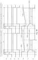
- FIG. 2 B illustrates a schematic diagram of waveforms of signals and voltages in FIG. 2 A according to some embodiments of the present disclosure.
- FIG. 2 B shows two consecutive sensing periods, in which the capacitor under-test CT is not being touched during the first sensing period (i.e., the capacitance value is unchanged), and is being touched during the second sensing period (i.e., the capacitance value is changed).
- the signal S 1 and the signal S 2 are switched to an enabling level (e.g., a high level).
- an enabling level e.g., a high level.
- the switch SW 1 and the switch SW 2 are turned on.
- the switch SW 1 transmits the reference voltage VREF 1 to the positive input terminal of the amplifier circuit 110
- the switch SW 2 couples the negative input terminal of the amplifier circuit 110 to its output terminal.
- the level of the negative input terminal of the amplifier circuit 110 is equal to that of the positive input terminal of the amplifier circuit 110 due to virtual ground (or virtual short-circuit), such that the levels of the negative input terminal, the positive input terminal, and the output terminal of the amplifier circuit 110 are equal to the reference voltage VREF 1 , in which the voltage of the negative input terminal of the amplifier circuit 110 is labeled as the voltage VA.
- the capacitor under-test CT is charged by the reference voltage VREF 1 to store charges amounted to CT ⁇ VREF 1 , a voltage across two terminals of the feedback capacitor CFB is zero, and thus no charges are stored by the feedback capacitor CFB.
- the output voltage VO is equal to the reference voltage VREF 1 , and is thus lower than the reference voltage VREF 2 .
- the comparator circuit 140 outputs the control signal SC having a first level (e.g., high level).
- the digital control circuit 150 does not operate according to the control signal SC during the phase P 1 , the digital control circuit 150 does not operate mistakenly.
- the signal S 1 and the signal S 2 are switched to a disabling level (e.g., a low level), and the signal S 3 is switched to an enabling level (e.g., a high level).
- the signal S 4 is switched the enabling level (e.g., the high level).
- the switch SW 1 is not turned on in response to the signal S 1
- the switch SW 2 is not turned on in response to the signal S 2
- the switch SW 3 is turned on in response to the signal S 3 .
- the switch SW 1 stops transmitting the reference voltage VREF 1 to the positive input terminal of the amplifier circuit 110
- the switch SW 3 transmits the reference voltage VREF 2 to the positive input terminal of the amplifier circuit 110
- the negative input terminal of the amplifier circuit 110 is not coupled to the output terminal of the amplifier circuit 110 via the switch SW 2 .
- the level of the negative input terminal of the amplifier circuit 110 is pulled to reference voltage VREF 2 during the phase P 2 due to virtual ground.
- the capacitor under-test CT is charged by the reference voltage VREF 2 to store charges amounted to CT ⁇ VREF 2
- the voltage across the two terminals of the feedback capacitor CFB is a difference between reference voltage VREF 2 and the output voltage VO, and thus the feedback capacitor CFB stores charges amounted to CFB ⁇ (VREF 2 ⁇ VO).
- the output voltage VO is higher than the reference voltage VREF 2 in a brief period.
- the comparator circuit 140 may output the control signal SC having a second level (e.g., a low level). As the digital control circuit 150 does not operate according to the control signal SC during the phase P 2 , the digital control circuit 150 does not operate mistakenly.
- V ⁇ O V ⁇ R ⁇ E ⁇ F ⁇ 2 + ( V ⁇ R ⁇ E ⁇ F ⁇ 2 - V ⁇ R ⁇ E ⁇ F ⁇ 1 ) ⁇ C ⁇ T C ⁇ F ⁇ B ( 2 )
- the switch SW 3 is continuously turned on in response to the signal S 3 , and the switch SW 4 is turned on in response to the signal S 4 .
- the switch SW 3 continuously transmits the reference voltage VREF 2 to the positive input terminal of the amplifier circuit 110 , and the current source circuit 210 may transmit the current I int to the negative input terminal of the amplifier circuit 110 via the switch SW 4 to adjust the output voltage VO.
- the counter circuit 130 may start counting based on the enable signal EN.
- the comparator circuit 140 When the level of the output voltage VO is adjusted to be equal to (or lower than) the reference voltage VREF 2 (i.e., time T 4 ), the comparator circuit 140 outputs the control signal SC having the high level. In response to the control signal SC, the counter circuit 130 stops counting and outputs the count value CNT to the digital control circuit 150 , in order to determine whether the capacitance value of the capacitor under-test CT changes. In the above operations, the amount of charges stored in the capacitor under-test CT is not changed, and the amount of charges stored in the feedback capacitor CFB is changed from CFB ⁇ (VREF 2 ⁇ VO) to CFB ⁇ (VREF 2 ⁇ VREF 2 ).
- the period T is proportional to the capacitance value of the capacitor under-test CT.
- the count value CNT generated by the counter circuit 130 may be utilized to indicate the time length of the period T. If the count value CNT does not exceed a predetermined range (or is the same as the predetermined value), it indicates that the capacitor under-test CT is not being touched and thus capacitance value is unchanged.
- the time length of the period T is proportional to the voltage difference between the reference voltage VREF 1 and the reference voltage VREF 2 .
- the count value CNT is proportional to the voltage difference between the reference voltage VREF 1 and the reference voltage VREF 2 .
- the value of the reference voltage VREF 1 and that of the reference voltage VREF 2 may be adjusted according to practical system requirement(s).
- the capacitive sensing device 100 may perform the same operations again to determine whether the capacitance value of the capacitor under-test CT changes.
- the capacitor under-test CT is being touched to have a higher capacitance value.
- the output voltage VO is increased to a higher level during the phase P 2 in the second sensing period.
- the time length of the period T is longer, and the value of the count value CNT is higher.
- the count value CNT is proportional to the change of the capacitance value of the capacitor under-test CT. If the count value CNT exceeds the predetermined range (or is higher than a predetermined value), it indicates that the capacitor under-test CT is touched to have a capacitance value change.
- FIG. 3 A illustrates a circuit diagram of the capacitive sensing device 100 in FIG. 1 according to some embodiments of the present disclosure.
- the reference voltage VREF 2 is lower than the reference voltage VREF 1
- the switch circuitry 120 is configured to drain the current I int from the negative input terminal of the amplifier circuit 110 to ground during the third phase, in order to adjust the output voltage VO.
- the current source circuit 210 is coupled from the negative input terminal of the amplifier circuit 110 to ground via the switch SW 4 to drain the current I int from the negative input terminal of the amplifier circuit 110 to ground, in order to adjust the output voltage VO.
- FIG. 3 B illustrates a schematic diagram of waveforms of signals and voltages in FIG. 3 A according to some embodiments of the present disclosure. Similar to FIG. 2 B , FIG. 3 B shows two consecutive sensing periods, in which the capacitor under-test CT is not being touched during the first sensing period (i.e., the capacitance value is unchanged), and is being touched during the second sensing period (i.e., the capacitance value is changed.
- the reference voltage VREF 2 is set to be lower than the reference voltage VREF 1 . Accordingly, the comparator circuit 140 outputs the control signal SC having the low level when the output voltage VO is equal to or higher than the reference voltage VREF 2 , and thus the counter circuit 130 may be configured to stop counting in response to the control signal SC having the low level.
- the output voltage VO is getting lower from the reference voltage VREF 1 .
- the level of the output voltage VO is increased gradually to be equal to or higher than the reference voltage VREF 2 .
- Operations of switches SW 1 -SW 4 and the changes of amount of the charges in each of the capacitor under-test CT and the feedback capacitor CFB are similar to those in FIG. 2 B , and thus the repetitious descriptions are not further given.
- the period T is a period from when the switch SW 4 starts being turned on to when the output voltage VO is adjusted to be equal to or higher than the reference voltage VREF 2 .
- FIG. 4 illustrates a flow chart of a capacitive sensing method 400 according to some embodiments of the present disclosure.
- operation S 410 during a first phase, a first reference voltage is transmitted to a first input terminal of an amplifier circuit and a second input terminal of the amplifier circuit is coupled to an output terminal of the amplifier circuit, in which the second input terminal is further coupled to the output terminal via a switch circuitry and is coupled to ground via a capacitor under-test.
- a second reference voltage is transmitted to the first input terminal during a second phase.
- an output voltage of the output terminal is adjusted and a control signal is generated according to the output voltage and the second reference voltage.
- counting is started when entering the third phase and is stopped according to the control signal to generate a count value, in which the count value indicates a capacitance value change of the capacitor under-test.
- the above operations of the capacitive sensing method 400 can be understood with reference to above embodiments, and thus the repetitious descriptions are not further given.
- the above description of the capacitive sensing method 400 includes exemplary operations, but the operations of the capacitive sensing method 400 are not necessarily performed in the order described above. Operations of the capacitive sensing method 400 may be added, replaced, changed order, and/or eliminated, or the operations of the capacitive sensing method 400 may be executed simultaneously or partially simultaneously as appropriate, in accordance with the spirit and scope of various embodiments of the present disclosure.
- the capacitive sensing device and the capacitive sensing method provided in some embodiments of the present disclosure may utilize a counter to generate a count value that is able to indicate whether a capacitance value of the capacitor under-test changes. As a result, it is able to monitor the count value to determine whether the capacitor under-test is being touched.
- the functional blocks will preferably be implemented through circuits (either dedicated circuits, or general purpose circuits, which operate under the control of one or more processors and coded instructions), which will typically comprise transistors or other circuit elements that are configured in such a way as to control the operation of the circuitry in accordance with the functions and operations described herein.
- a compiler such as a register transfer language (RTL) compiler.
- RTL compilers operate upon scripts that closely resemble assembly language code, to compile the script into a form that is used for the layout or fabrication of the ultimate circuitry. Indeed, RTL is well known for its role and use in the facilitation of the design process of electronic and digital systems.
Landscapes
- Engineering & Computer Science (AREA)
- General Engineering & Computer Science (AREA)
- Theoretical Computer Science (AREA)
- Physics & Mathematics (AREA)
- General Physics & Mathematics (AREA)
- Human Computer Interaction (AREA)
- Measurement Of Resistance Or Impedance (AREA)
- Electronic Switches (AREA)
Abstract
Description
VREF2×CT−VREF1×CT=—(VREF2−VO)×CFB (1)
I int ×T=(VREF2−VREF2)×CFB−(VREF2−VO)×CFB (3)
Claims (20)
Applications Claiming Priority (2)
| Application Number | Priority Date | Filing Date | Title |
|---|---|---|---|
| TW111120516 | 2022-06-01 | ||
| TW111120516A TWI825758B (en) | 2022-06-01 | 2022-06-01 | Capacitive sensing device and capacitive sensing method |
Publications (2)
| Publication Number | Publication Date |
|---|---|
| US20230393693A1 US20230393693A1 (en) | 2023-12-07 |
| US11966531B2 true US11966531B2 (en) | 2024-04-23 |
Family
ID=88976454
Family Applications (1)
| Application Number | Title | Priority Date | Filing Date |
|---|---|---|---|
| US18/197,750 Active US11966531B2 (en) | 2022-06-01 | 2023-05-16 | Capacitive sensing device and capacitive sensing method |
Country Status (2)
| Country | Link |
|---|---|
| US (1) | US11966531B2 (en) |
| TW (1) | TWI825758B (en) |
Citations (12)
| Publication number | Priority date | Publication date | Assignee | Title |
|---|---|---|---|---|
| US20120049868A1 (en) * | 2010-08-24 | 2012-03-01 | Cypress Semiconductor Corporation | Capacitance sensing systems, circuits and methods that include current conveyor based oscillators |
| US20120268415A1 (en) * | 2011-04-19 | 2012-10-25 | Anton Konovalov | Method and apparatus to improve noise immunity of a touch sense array |
| US20130207677A1 (en) * | 2010-09-28 | 2013-08-15 | Fujikura, Ltd. | Electrostatic capacitance sensor and method for determining failure of electrostatic capacitance sensor |
| US8810546B1 (en) * | 2012-09-26 | 2014-08-19 | Cypress Semiconductor Corporation | Touchscreen panel frequency response determination |
| US9151792B1 (en) | 2014-05-29 | 2015-10-06 | Cyress Semiconductor Corporation | High-voltage, high-sensitivity self-capacitance sensing |
| US20150317028A1 (en) * | 2014-05-02 | 2015-11-05 | Semiconductor Energy Laboratory Co., Ltd. | Display device and input/output device |
| US20170003777A1 (en) * | 2015-06-30 | 2017-01-05 | Synaptics Incorporated | Active matrix capacitive fingerprint sensor with 1-tft pixel architecture for display integration |
| CN106598370A (en) | 2017-01-19 | 2017-04-26 | 北京集创北方科技股份有限公司 | Touch detection circuit and touch device thereof |
| CN107092407A (en) | 2017-04-12 | 2017-08-25 | 北京集创北方科技股份有限公司 | Inductance capacitance measurement apparatus |
| US9823798B2 (en) | 2016-04-08 | 2017-11-21 | Nxp Usa, Inc. | Capacitive sensor device and method of operation |
| US20200220543A1 (en) | 2019-01-08 | 2020-07-09 | Raydium Semiconductor Corporation | Capacitive touch sensing circuit |
| US20210055832A1 (en) * | 2017-08-08 | 2021-02-25 | Cambridge Touch Technologies Ltd. | Touch panel pressure detection |
Family Cites Families (4)
| Publication number | Priority date | Publication date | Assignee | Title |
|---|---|---|---|---|
| TWI395125B (en) * | 2009-07-14 | 2013-05-01 | Sonix Technology Co Ltd | Capacitive touch sensing circuit |
| US8866499B2 (en) * | 2009-08-27 | 2014-10-21 | Analog Devices, Inc. | System and method for measuring capacitance |
| US9244569B2 (en) * | 2010-03-31 | 2016-01-26 | Stmicroelectronics Asia Pacific Pte Ltd | Capacitive sensing analog front end |
| TWI569186B (en) * | 2014-10-21 | 2017-02-01 | 財團法人工業技術研究院 | Touch sensing method and touch sensing apparatus |
-
2022
- 2022-06-01 TW TW111120516A patent/TWI825758B/en active
-
2023
- 2023-05-16 US US18/197,750 patent/US11966531B2/en active Active
Patent Citations (18)
| Publication number | Priority date | Publication date | Assignee | Title |
|---|---|---|---|---|
| US8729913B2 (en) * | 2010-08-24 | 2014-05-20 | Cypress Semiconductor Corporation | Capacitance sensing systems, circuits and methods that include current conveyor based oscillators |
| US20120049868A1 (en) * | 2010-08-24 | 2012-03-01 | Cypress Semiconductor Corporation | Capacitance sensing systems, circuits and methods that include current conveyor based oscillators |
| US9274154B2 (en) * | 2010-09-28 | 2016-03-01 | Fujikura Ltd. | Electrostatic capacitance sensor and method for determining failure of electrostatic capacitance sensor |
| US20130207677A1 (en) * | 2010-09-28 | 2013-08-15 | Fujikura, Ltd. | Electrostatic capacitance sensor and method for determining failure of electrostatic capacitance sensor |
| US20120268415A1 (en) * | 2011-04-19 | 2012-10-25 | Anton Konovalov | Method and apparatus to improve noise immunity of a touch sense array |
| US9092098B2 (en) * | 2011-04-19 | 2015-07-28 | Cypress Semiconductor Corporation | Method and apparatus to improve noise immunity of a touch sense array |
| US8810546B1 (en) * | 2012-09-26 | 2014-08-19 | Cypress Semiconductor Corporation | Touchscreen panel frequency response determination |
| US20150317028A1 (en) * | 2014-05-02 | 2015-11-05 | Semiconductor Energy Laboratory Co., Ltd. | Display device and input/output device |
| US10521032B2 (en) * | 2014-05-02 | 2019-12-31 | Semiconductor Energy Laboratory Co., Ltd. | Display device and input/output device |
| US9151792B1 (en) | 2014-05-29 | 2015-10-06 | Cyress Semiconductor Corporation | High-voltage, high-sensitivity self-capacitance sensing |
| US20170003777A1 (en) * | 2015-06-30 | 2017-01-05 | Synaptics Incorporated | Active matrix capacitive fingerprint sensor with 1-tft pixel architecture for display integration |
| US9958993B2 (en) * | 2015-06-30 | 2018-05-01 | Synaptics Incorporated | Active matrix capacitive fingerprint sensor with 1-TFT pixel architecture for display integration |
| US9823798B2 (en) | 2016-04-08 | 2017-11-21 | Nxp Usa, Inc. | Capacitive sensor device and method of operation |
| CN106598370A (en) | 2017-01-19 | 2017-04-26 | 北京集创北方科技股份有限公司 | Touch detection circuit and touch device thereof |
| CN107092407A (en) | 2017-04-12 | 2017-08-25 | 北京集创北方科技股份有限公司 | Inductance capacitance measurement apparatus |
| US20210055832A1 (en) * | 2017-08-08 | 2021-02-25 | Cambridge Touch Technologies Ltd. | Touch panel pressure detection |
| US11481060B2 (en) * | 2017-08-08 | 2022-10-25 | Cambridge Touch Technologies Ltd. | Touch panel pressure detection |
| US20200220543A1 (en) | 2019-01-08 | 2020-07-09 | Raydium Semiconductor Corporation | Capacitive touch sensing circuit |
Also Published As
| Publication number | Publication date |
|---|---|
| US20230393693A1 (en) | 2023-12-07 |
| TW202349188A (en) | 2023-12-16 |
| TWI825758B (en) | 2023-12-11 |
Similar Documents
| Publication | Publication Date | Title |
|---|---|---|
| US9652104B2 (en) | Capacitance voltage conversion circuit, input apparatus using the same, electronic instrument, and capacitance voltage conversion method | |
| US10845926B2 (en) | Capacitance detecting circuit, touch device and terminal device | |
| US10627436B2 (en) | Capacitance sensing circuits | |
| US10942606B2 (en) | Touch sensing device of current driving type | |
| US20070052428A1 (en) | Object sensing | |
| US9197207B2 (en) | Touch sensor circuit and touch display device | |
| US9086712B2 (en) | Device and method for compensating for voltage drops | |
| US10684726B2 (en) | Capacitive touch sensing circuit and charge compensation method thereof | |
| US11758076B2 (en) | Clock generator device, image processing chip, and clock signal calibration method | |
| US11966531B2 (en) | Capacitive sensing device and capacitive sensing method | |
| US11843401B2 (en) | Transmitter with slew rate control | |
| US20120139529A1 (en) | Readout apparatus for current type touch panel | |
| US20220200588A1 (en) | Current steering comparator and capacitor control method | |
| US11777477B2 (en) | Digital circuit device and voltage drop detector circuitry | |
| US9030246B2 (en) | Semiconductor device | |
| US20220247399A1 (en) | Reliability detection device and reliability detection method | |
| CN106325625B (en) | Mutual capacitance touch screen capable of automatically adjusting width of sensing window | |
| US20070021846A1 (en) | Button device | |
| US20220360256A1 (en) | Ramp signal calibration device | |
| US20220276286A1 (en) | Voltage hold circuit, voltage monitoring circuit, and semiconductor integrated circuit | |
| CN117234349A (en) | Capacitance sensing device and capacitance sensing method | |
| US7142146B2 (en) | Method and system for reducing interference between analog circuits operating from a common power supply | |
| CN114924608A (en) | Reference voltage generating circuit | |
| CN116094509A (en) | Touch state detection circuit, method and electronic system | |
| JPS585026A (en) | Semiconductor integrated circuit |
Legal Events
| Date | Code | Title | Description |
|---|---|---|---|
| AS | Assignment |
Owner name: REALTEK SEMICONDUCTOR CORPORATION, TAIWAN Free format text: ASSIGNMENT OF ASSIGNORS INTEREST;ASSIGNOR:TSAI, HSU-MING;REEL/FRAME:063649/0299 Effective date: 20230511 |
|
| FEPP | Fee payment procedure |
Free format text: ENTITY STATUS SET TO UNDISCOUNTED (ORIGINAL EVENT CODE: BIG.); ENTITY STATUS OF PATENT OWNER: LARGE ENTITY |
|
| STPP | Information on status: patent application and granting procedure in general |
Free format text: DOCKETED NEW CASE - READY FOR EXAMINATION |
|
| STPP | Information on status: patent application and granting procedure in general |
Free format text: NOTICE OF ALLOWANCE MAILED -- APPLICATION RECEIVED IN OFFICE OF PUBLICATIONS |
|
| ZAAB | Notice of allowance mailed |
Free format text: ORIGINAL CODE: MN/=. |
|
| STPP | Information on status: patent application and granting procedure in general |
Free format text: AWAITING TC RESP., ISSUE FEE NOT PAID |
|
| STPP | Information on status: patent application and granting procedure in general |
Free format text: PUBLICATIONS -- ISSUE FEE PAYMENT RECEIVED |
|
| STPP | Information on status: patent application and granting procedure in general |
Free format text: PUBLICATIONS -- ISSUE FEE PAYMENT VERIFIED |
|
| STCF | Information on status: patent grant |
Free format text: PATENTED CASE |