US11940407B2 - Micro-sensor for detecting chemical species and associated manufacturing method - Google Patents
Micro-sensor for detecting chemical species and associated manufacturing method Download PDFInfo
- Publication number
- US11940407B2 US11940407B2 US17/044,205 US201917044205A US11940407B2 US 11940407 B2 US11940407 B2 US 11940407B2 US 201917044205 A US201917044205 A US 201917044205A US 11940407 B2 US11940407 B2 US 11940407B2
- Authority
- US
- United States
- Prior art keywords
- microsensor
- dielectric layer
- active layer
- silicon
- nanometers
- Prior art date
- Legal status (The legal status is an assumption and is not a legal conclusion. Google has not performed a legal analysis and makes no representation as to the accuracy of the status listed.)
- Active, expires
Links
Images

Classifications
-
- G—PHYSICS
- G01—MEASURING; TESTING
- G01N—INVESTIGATING OR ANALYSING MATERIALS BY DETERMINING THEIR CHEMICAL OR PHYSICAL PROPERTIES
- G01N27/00—Investigating or analysing materials by the use of electric, electrochemical, or magnetic means
- G01N27/26—Investigating or analysing materials by the use of electric, electrochemical, or magnetic means by investigating electrochemical variables; by using electrolysis or electrophoresis
- G01N27/403—Cells and electrode assemblies
- G01N27/414—Ion-sensitive or chemical field-effect transistors, i.e. ISFETS or CHEMFETS
- G01N27/4148—Integrated circuits therefor, e.g. fabricated by CMOS processing
-
- B—PERFORMING OPERATIONS; TRANSPORTING
- B01—PHYSICAL OR CHEMICAL PROCESSES OR APPARATUS IN GENERAL
- B01L—CHEMICAL OR PHYSICAL LABORATORY APPARATUS FOR GENERAL USE
- B01L3/00—Containers or dishes for laboratory use, e.g. laboratory glassware; Droppers
- B01L3/50—Containers for the purpose of retaining a material to be analysed, e.g. test tubes
- B01L3/502—Containers for the purpose of retaining a material to be analysed, e.g. test tubes with fluid transport, e.g. in multi-compartment structures
- B01L3/5027—Containers for the purpose of retaining a material to be analysed, e.g. test tubes with fluid transport, e.g. in multi-compartment structures by integrated microfluidic structures, i.e. dimensions of channels and chambers are such that surface tension forces are important, e.g. lab-on-a-chip
- B01L3/502715—Containers for the purpose of retaining a material to be analysed, e.g. test tubes with fluid transport, e.g. in multi-compartment structures by integrated microfluidic structures, i.e. dimensions of channels and chambers are such that surface tension forces are important, e.g. lab-on-a-chip characterised by interfacing components, e.g. fluidic, electrical, optical or mechanical interfaces
-
- H01L21/30604—
-
- H01L21/76254—
-
- H—ELECTRICITY
- H10—SEMICONDUCTOR DEVICES; ELECTRIC SOLID-STATE DEVICES NOT OTHERWISE PROVIDED FOR
- H10P—GENERIC PROCESSES OR APPARATUS FOR THE MANUFACTURE OR TREATMENT OF DEVICES COVERED BY CLASS H10
- H10P50/00—Etching of wafers, substrates or parts of devices
- H10P50/60—Wet etching
- H10P50/64—Wet etching of semiconductor materials
- H10P50/642—Chemical etching
-
- H—ELECTRICITY
- H10—SEMICONDUCTOR DEVICES; ELECTRIC SOLID-STATE DEVICES NOT OTHERWISE PROVIDED FOR
- H10P—GENERIC PROCESSES OR APPARATUS FOR THE MANUFACTURE OR TREATMENT OF DEVICES COVERED BY CLASS H10
- H10P90/00—Preparation of wafers not covered by a single main group of this subclass, e.g. wafer reinforcement
- H10P90/19—Preparing inhomogeneous wafers
- H10P90/1904—Preparing vertically inhomogeneous wafers
- H10P90/1906—Preparing SOI wafers
- H10P90/1914—Preparing SOI wafers using bonding
- H10P90/1916—Preparing SOI wafers using bonding with separation or delamination along an ion implanted layer, e.g. Smart-cut
-
- H—ELECTRICITY
- H10—SEMICONDUCTOR DEVICES; ELECTRIC SOLID-STATE DEVICES NOT OTHERWISE PROVIDED FOR
- H10W—GENERIC PACKAGES, INTERCONNECTIONS, CONNECTORS OR OTHER CONSTRUCTIONAL DETAILS OF DEVICES COVERED BY CLASS H10
- H10W10/00—Isolation regions in semiconductor bodies between components of integrated devices
- H10W10/10—Isolation regions comprising dielectric materials
- H10W10/181—Semiconductor-on-insulator [SOI] isolation regions, e.g. buried oxide regions of SOI wafers
-
- B—PERFORMING OPERATIONS; TRANSPORTING
- B01—PHYSICAL OR CHEMICAL PROCESSES OR APPARATUS IN GENERAL
- B01L—CHEMICAL OR PHYSICAL LABORATORY APPARATUS FOR GENERAL USE
- B01L2200/00—Solutions for specific problems relating to chemical or physical laboratory apparatus
- B01L2200/12—Specific details about manufacturing devices
-
- H01L29/16—
-
- H01L29/161—
-
- H01L29/20—
-
- H01L29/2003—
-
- H—ELECTRICITY
- H10—SEMICONDUCTOR DEVICES; ELECTRIC SOLID-STATE DEVICES NOT OTHERWISE PROVIDED FOR
- H10D—INORGANIC ELECTRIC SEMICONDUCTOR DEVICES
- H10D62/00—Semiconductor bodies, or regions thereof, of devices having potential barriers
- H10D62/80—Semiconductor bodies, or regions thereof, of devices having potential barriers characterised by the materials
- H10D62/83—Semiconductor bodies, or regions thereof, of devices having potential barriers characterised by the materials being Group IV materials, e.g. B-doped Si or undoped Ge
-
- H—ELECTRICITY
- H10—SEMICONDUCTOR DEVICES; ELECTRIC SOLID-STATE DEVICES NOT OTHERWISE PROVIDED FOR
- H10D—INORGANIC ELECTRIC SEMICONDUCTOR DEVICES
- H10D62/00—Semiconductor bodies, or regions thereof, of devices having potential barriers
- H10D62/80—Semiconductor bodies, or regions thereof, of devices having potential barriers characterised by the materials
- H10D62/83—Semiconductor bodies, or regions thereof, of devices having potential barriers characterised by the materials being Group IV materials, e.g. B-doped Si or undoped Ge
- H10D62/832—Semiconductor bodies, or regions thereof, of devices having potential barriers characterised by the materials being Group IV materials, e.g. B-doped Si or undoped Ge being Group IV materials comprising two or more elements, e.g. SiGe
-
- H—ELECTRICITY
- H10—SEMICONDUCTOR DEVICES; ELECTRIC SOLID-STATE DEVICES NOT OTHERWISE PROVIDED FOR
- H10D—INORGANIC ELECTRIC SEMICONDUCTOR DEVICES
- H10D62/00—Semiconductor bodies, or regions thereof, of devices having potential barriers
- H10D62/80—Semiconductor bodies, or regions thereof, of devices having potential barriers characterised by the materials
- H10D62/85—Semiconductor bodies, or regions thereof, of devices having potential barriers characterised by the materials being Group III-V materials, e.g. GaAs
-
- H—ELECTRICITY
- H10—SEMICONDUCTOR DEVICES; ELECTRIC SOLID-STATE DEVICES NOT OTHERWISE PROVIDED FOR
- H10D—INORGANIC ELECTRIC SEMICONDUCTOR DEVICES
- H10D62/00—Semiconductor bodies, or regions thereof, of devices having potential barriers
- H10D62/80—Semiconductor bodies, or regions thereof, of devices having potential barriers characterised by the materials
- H10D62/85—Semiconductor bodies, or regions thereof, of devices having potential barriers characterised by the materials being Group III-V materials, e.g. GaAs
- H10D62/8503—Nitride Group III-V materials, e.g. AlN or GaN
Definitions
- the present disclosure relates to the field of microsensors for detecting chemical species in ionic form that are present in a fluid. It relates, in particular, to a microsensor comprising an ion-sensitive field-effect transistor and comprising integrated microfluidic channels for transporting the fluid.
- ISFET Ion-sensitive field-effect transistors
- the gate of the transistor is placed in contact with the chemical solution to be analyzed; the chemical species present in the solution modify the electrochemical potential in the vicinity of the gate, and may thus influence the current circulating between the drain and the source of the transistor.
- the conduction characteristics of the ISFET are therefore capable of changing as a function of the concentration of the ions in contact with the gate.
- the conventional approach involves bringing the chemical solution into contact with the gate of the transistor (or with the gate oxide), at the front face of the transistor, i.e., in the active region of the component, where sensitive elements of the transistor are formed (source electrode, drain electrode, metal contacts, etc.)
- sensitive elements of the transistor source electrode, drain electrode, metal contacts, etc.
- local encapsulation layers are used to insulate these elements from the chemical solution, infiltrations may be the cause of premature wear or failure of the transistor.
- the formation of such encapsulation layers further complicates the production process.
- document WO 00/51180 proposes the formation of an ISFET on an SOI (silicon on insulator) substrate, then the formation of an insulating support layer on the front face of the transistor and finally the partial or complete removal of the silicon substrate to expose the oxide layer of the SOI; the oxide layer is then placed in contact with the chemical solution.
- This approach avoids bringing the front face of the transistor into contact with a chemical solution and therefore prevents risks of infiltration.
- it has the drawback of carrying out a step of removing, by etching, several hundreds of microns of the silicon substrate. This removal may be aggressive for the active layer (silicon surface layer of the SOI) and the sensitive elements of the transistor.
- the present disclosure aims to overcome all or some of the aforementioned drawbacks, and relates to a microsensor for chemical analysis, based on a field-effect transistor, and to the associated fabrication process.
- the present disclosure relates to a microsensor for detecting ions in a fluid, comprising:
- the present disclosure also relates to a process for fabricating a microsensor for detecting ions in a fluid, comprising:
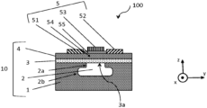
- FIGS. 1 a and 1 b present microsensors in accordance with the present disclosure
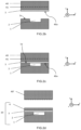
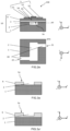
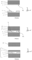
- FIGS. 2 a to 2 e and 3 a to 3 d present steps of the process for fabricating a microsensor in accordance with the present disclosure.
- the same references in the figures might be used for elements of the same type.
- the figures are schematic representations which, for the sake of legibility, are not to scale.
- the thicknesses of the layers along the z-axis are not to scale with respect to their lateral dimensions along the x- and y-axes; and the relative thicknesses of the layers with respect to one another are not necessarily respected in the figures.
- the present disclosure relates to a microsensor 100 for detecting ions in a fluid.
- the microsensor 100 comprises a structure 10 comprising an active layer 4 , positioned on a dielectric layer 3 , itself positioned on a support substrate 1 ( FIG. 1 a ).
- the active layer 4 is intended to contain and/or support at least one microelectronic component, in particular, a field-effect transistor (FET).
- FET field-effect transistor
- the active layer 4 may be based on a single material or may include several layers of different materials.
- the active layer 4 is formed of at least one semiconductor material selected from silicon, silicon-germanium, germanium, III-V compounds (arsenides, phosphides, nitrides, etc.) And it has a thickness between a few nanometers and a few hundreds of nanometers.
- the support substrate 1 may be based on a semiconductor or an insulating material, such as silicon, germanium, silicon carbide, gallium arsenide, indium phosphide, sapphire or glass.
- the support substrate 1 is formed of silicon.
- the structure 10 further comprises at least one buried cavity 2 , formed in the support substrate 1 and positioned beneath the dielectric layer 3 . A portion of the surface 3 a of the dielectric layer 3 adjacent the buried cavity 2 is, therefore, free.
- the microsensor 100 also comprises a field-effect transistor 5 (also referred to herein as “FET 5 ”) formed in and on the active layer 4 of the structure 10 . It has a source 51 , a drain 52 , an active region 54 between the source 51 and the drain 52 , and a gate 53 positioned above the active region 54 .
- the active region 54 is formed in the active layer 4 , it comprises a conduction channel in which the current is capable of flowing, between the source 51 and the drain 52 , when the field-effect transistor 5 is in an on-state.
- the gate 53 is positioned on the insulating layer 55 (gate oxide), which separates it from the active layer 4 .
- the active layer 4 is thin.
- it could have a thickness of 15 nm.
- the field-effect transistor 5 is advantageously produced according to conventional CMOS technology in and on the active layer 4 ; it is, for example, of MOSFET type and operates in fully depleted mode.
- the field-effect transistor 5 is advantageously produced according to FDSOI (fully depleted SOI) architecture.
- the field-effect transistor 5 maybe of HEMT (high electron mobility transistor) type.
- An FET transistor for the chemical detection of ions must be very sensitive.
- the threshold voltage of the transistor must preferably be sensitive to the variation of the electrochemical potential in the vicinity of the gate, to detect as precisely as possible a variation in concentration of ions in the solution brought into contact with the gate.
- An FET 5 in “fully depleted” mode of the microsensor 100 produced on an active layer 4 , in particular, made of silicon, and a dielectric layer 3 , have features perfectly suitable for this application.
- the gate 53 is produced substantially plum with the buried cavity 2 and all or some of the active region 54 is located above the buried cavity 2 .
- the buried cavity 2 is intended to receive the fluid to be analyzed and to bring it into contact with the dielectric layer 3 .
- the buried cavity 2 could have lateral dimensions (in the (x, y) plane in the figures) between around 100 nanometers and a few tens of microns and a depth (along the z axis in the figures) between a few tens of nanometers and a few hundreds of microns.
- a buried cavity 2 could have a width (along the y axis in the figures) of around 150 nm, a length (along the x axis in the figures) of around 500 nm and a depth on the order of 150 nm.
- the dielectric layer 3 is formed of at least one insulating material selected from silicon dioxide, silicon nitride, an oxynitride, hafnium oxide (HfO 2 ), alumina (Al 2 O 3 ), tantalum oxide (Ta 2 O 5 ) or a stack of layers of these materials.
- the dielectric layer 3 has a thickness of between a few angstroms and a few tens of nanometers.
- the ions present in the fluid will modify the electrochemical potential at the surface 3 a of the dielectric layer 3 .
- the FET 5 then operates with a dual gate: the upper gate 53 , which may be biased at a certain potential and the lower chemical gate, the potential of which (at the surface 3 a of the dielectric layer 3 ) is influenced by the presence and the concentration of the ions of the fluid contained in the buried cavity 2 .
- the insulating material of the dielectric layer 3 is selected as a function of the type of ions to be detected in the fluid.
- the buried cavity 2 comprises a constriction 2 a in the vicinity of the dielectric layer 3 ; at this constriction 2 a , the cavity 2 has lateral dimensions corresponding substantially to the dimensions of the gate 53 .
- the buried cavity 2 further comprises a flared portion 2 b in its deeper zone. This flared portion 2 b promotes the circulation of the fluid.
- the constriction 2 a having reduced lateral dimensions, promotes the mechanical strength of the stack of dielectric and active layers 3 , 4 positioned on top of the buried cavity 2 and may simplify the fabrication of the structure 10 and/or of the microsensor 100 .
- a buried cavity 2 could have, at the constriction 2 a , a width (along the y axis) of around 100 nm, a length (along the x axis) of around 200 nm, and at the flared portion 2 b , a width (along they axis) of around 1000 nm, a length (along the x axis) of around 2000 nm. It could furthermore have a depth of the order of 500 nm.
- the (at least one) buried cavity 2 is connected to a network of buried channels 20 formed in the support substrate 1 , in order to continuously or periodically transport the fluid.
- the network comprises a fluid inlet 21 and a fluid outlet 22 ( FIG. 2 e ).
- An external pumping system makes it possible to circulate the fluid in the network of buried channels 20 , in order to convey it into the buried cavity 2 .
- the fluid is removed from the buried cavity 2 by pumping or flushed from the buried cavity 2 by injecting a rinsing solution into the network of buried channels 20 .
- the present disclosure also relates to a process for fabricating the microsensor 100 for detecting ions in a fluid.
- the fabrication process comprises a first step of providing a structure 10 comprising an active layer 4 , positioned on a dielectric layer 3 , itself positioned on a support substrate 1 .
- the structure 10 comprises at least one buried cavity 2 , formed in the support substrate 1 and positioned beneath the dielectric layer 3 .
- this first step includes the formation, on a first face 1 a of the support substrate 1 , of the (at least one) buried cavity 2 , by etching ( FIG. 2 a ).
- a masking layer (not represented) is deposited on the first face 1 a and removed locally at the locations intended to be etched in order to form the buried cavity (or cavities) 2 .
- the network of buried channels 20 communicating with the buried cavity 2 is preferably produced at the same time.
- the support substrate 1 comprises an intermediate layer 6 at the first face 1 a thereof.
- the buried cavity (or cavities) 2 and the network of buried channels 20 are formed in the intermediate layer 6 .
- the intermediate layer 6 is preferably formed of at least one insulating material selected from silicon dioxide, silicon nitride, an oxynitride, hafnium oxide (HfO 2 ), alumina (Al 2 O 3 ), tantalum oxide (Ta 2 O 5 ) or a stack of layers of these materials.
- a buried cavity 2 could have lateral dimensions (in the (x, y) plane in the figures) between around 100 nanometers and a few tens of microns and a depth (along the z axis in the figures) between a few tens of nanometers and a few hundreds of microns.
- the buried channels 20 could have dimensions in similar ranges.
- the first step of the process comprises the provision of a donor substrate 40 , having a first face 40 a and comprising a dielectric layer 3 ( FIGS. 2 b , 3 b ).
- the dielectric layer 3 may be produced by thermal growth or by deposition, depending on the nature of the material(s) forming it and depending on the nature of the donor substrate 40 .
- the dielectric layer 3 is preferably formed of at least one insulating material selected from silicon dioxide, silicon nitride, an oxynitride, hafnium oxide (HfO 2 ), alumina (Al 2 O 3 ), tantalum oxide (Ta 2 O 5 ) or a stack of layers of these materials.
- the donor substrate 40 is preferably formed of at least one semiconductor material selected from silicon, silicon-germanium, germanium, III-V compounds (arsenides, phosphides, nitrides, etc.).
- the active layer 4 In order to form the active layer 4 from the donor substrate 40 , use will preferably be made of a transfer process especially suitable for thin to very thin layers and that provides a good layer thickness uniformity and a very good crystalline and surface quality.
- the SMART CUT® process may be used.
- Light species hydrogen and/or helium
- the joining of the first face 1 a of the support substrate 1 comprising the buried cavity (or cavities) 2 and the network of buried channels 20 , to the first face 40 a of a donor substrate 40 comprising a dielectric layer 3 is then carried out ( FIGS. 2 c , 3 c ).
- the buried cavity 2 and the network of buried channels 20 are thus buried in the joined structure.
- the joining is carried out by direct bonding, molecular adhesion of the two surfaces brought into contact.
- the principle of molecular adhesion which is well known in the prior art, will not be described in further detail here. Note that a very good surface finish (cleanness, low roughness, etc.) of the substrates to be joined is required, in order to obtain a good final quality of the structure 10 .
- the first step of the process comprises the thinning of the donor substrate 40 , so as to form the active layer 4 .
- the separation at the fragile buried layer 41 may take place during a heat treatment, for example, between 250° C. and 550° C., and/or under mechanical stress. This separation makes it possible, on the one hand, to form the structure 10 comprising the active layer 4 positioned on the dielectric layer 3 , itself positioned on the support substrate 1 , and, on the other hand, to form a residual donor substrate 40 ′ ( FIGS. 2 d , 3 d ).
- Finishing steps for example, thermal oxidation, thermal smoothing, or others are applied to the separated surface of the active layer 4 , so as to give it the required quality (in terms of thickness, uniformity, crystalline quality, roughness, defectivity) for the subsequent production of the FET transistors.
- the fabrication process comprises a second step of producing a field-effect transistor 5 having a source 51 , a drain 52 , an active region 54 formed in the active layer 4 and extending between the source 51 and the drain 52 .
- the transistor 5 also comprises a gate 53 positioned above the active region 54 , plumb with the (at least one) cavity 2 ( FIG. 2 e ).
- the alignment between the cavity 2 and the gate 53 of the transistor 5 could be easily achieved by using the alignment marks produced during the formation of the cavity 2 and the channels 20 on the support substrate 1 .
- each cavity 2 has a dimension, in the (x, y) plane, of less than 1000 nm or even of less than 200 nm, it being possible for the other dimension to range up to a few tens of microns ( FIG. 2 e ).
- the smallest dimension (width) is along the source 51 -drain 52 axis (y axis in the figures).
- the largest dimension (length) preferably corresponds to the width of the active region 54 , i.e., to the size of the source 51 , drain 52 and gate 53 electrodes (along the x axis in the figures).
- Such a configuration of the buried cavity 2 in the (x, y) plane is favorable to the mechanical strength of the stack portions of active layer 4 and dielectric layer 3 that are suspended above the buried cavity 2 .
- the cavity (or cavities) 2 and the network of channels 20 , produced in the support substrate 1 could be filled by a sacrificial material.
- the production of the structure 10 and of the transistor 5 of the microsensor 100 is carried out even though the cavities 2 are filled with the material.
- a step of etching in the active layer 4 and the dielectric layer 3 makes it possible to access the cavity (cavities) 2 and channels 20 ; the sacrificial material is chemically etched in order to empty the cavity (cavities) 2 and channels 20 , an encapsulation layer protecting the sensitive elements on the front face of the transistor 5 .
- the sacrificial material is selected so that it is preferably attacked by the chemical etching, compared to the support substrate 1 and the dielectric layer 3 .
- the microsensor 100 may comprise several field-effect transistors 5 , in particular, for increasing the effectiveness of processing the electrical signal expressing the detection of ions.
- These transistors 5 may share, for example, one and the same lower chemical gate (at the surface 3 a of the dielectric layer 3 ) positioned on one and the same cavity 2 in order to improve the sensitivity of the microsensor 100 .
- the microsensor 100 comprises at least one cavity 2 and a network of integrated channels 20 , buried beneath an FET 5 ; the latter is configured to operate with an upper gate 53 and lower chemical gate (at the surface 3 a of the dielectric layer 3 ) the electrochemical potential of which is influenced by the presence and the concentration of chemical species in the cavity 2 .
- the presence of the cavity (cavities) 2 and network of channels 20 in the support substrate 1 of the structure 10 used for the production of the transistor 5 avoids the deep etching steps of the prior art for exposing the dielectric layer after the formation of the transistor.
- the microsensor 100 may be used for the detection of chemical species in ionic form in a gaseous or liquid fluid.
- applications could be found in the field of gas detection or else of biological sensors for the detection of analytes in solution or the measurement of pH.
Landscapes
- Chemical & Material Sciences (AREA)
- Health & Medical Sciences (AREA)
- Engineering & Computer Science (AREA)
- Microelectronics & Electronic Packaging (AREA)
- Life Sciences & Earth Sciences (AREA)
- Chemical Kinetics & Catalysis (AREA)
- General Health & Medical Sciences (AREA)
- Analytical Chemistry (AREA)
- Pathology (AREA)
- Molecular Biology (AREA)
- Electrochemistry (AREA)
- Biochemistry (AREA)
- Computer Hardware Design (AREA)
- General Physics & Mathematics (AREA)
- Physics & Mathematics (AREA)
- Immunology (AREA)
- Hematology (AREA)
- Dispersion Chemistry (AREA)
- Clinical Laboratory Science (AREA)
- Thin Film Transistor (AREA)
- Investigating Or Analyzing Materials By The Use Of Electric Means (AREA)
- General Chemical & Material Sciences (AREA)
- Element Separation (AREA)
- Insulated Gate Type Field-Effect Transistor (AREA)
Applications Claiming Priority (3)
| Application Number | Priority Date | Filing Date | Title |
|---|---|---|---|
| FR1852783A FR3079616B1 (fr) | 2018-03-30 | 2018-03-30 | Micro-capteur pour detecter des especes chimiques et procede de fabrication associe |
| FR1852783 | 2018-03-30 | ||
| PCT/FR2019/050610 WO2019186027A1 (fr) | 2018-03-30 | 2019-03-19 | Micro-capteur pour détecter des espèces chimiques et procédé de fabrication associé |
Publications (2)
| Publication Number | Publication Date |
|---|---|
| US20210132002A1 US20210132002A1 (en) | 2021-05-06 |
| US11940407B2 true US11940407B2 (en) | 2024-03-26 |
Family
ID=62684890
Family Applications (1)
| Application Number | Title | Priority Date | Filing Date |
|---|---|---|---|
| US17/044,205 Active 2041-05-10 US11940407B2 (en) | 2018-03-30 | 2019-03-19 | Micro-sensor for detecting chemical species and associated manufacturing method |
Country Status (7)
| Country | Link |
|---|---|
| US (1) | US11940407B2 (fr) |
| EP (1) | EP3775862B1 (fr) |
| KR (1) | KR102813268B1 (fr) |
| CN (1) | CN111971552B (fr) |
| FR (1) | FR3079616B1 (fr) |
| TW (1) | TWI794449B (fr) |
| WO (1) | WO2019186027A1 (fr) |
Cited By (1)
| Publication number | Priority date | Publication date | Assignee | Title |
|---|---|---|---|---|
| US12339247B2 (en) | 2022-04-07 | 2025-06-24 | Globalfoundries U.S. Inc. | Field effect transistor with buried fluid-based gate and method |
Families Citing this family (7)
| Publication number | Priority date | Publication date | Assignee | Title |
|---|---|---|---|---|
| CN111415993B (zh) * | 2020-03-16 | 2023-11-21 | 中国科学院微电子研究所 | 一种多介质检测传感器及其制作方法 |
| FR3115278B1 (fr) * | 2020-10-16 | 2024-02-16 | Soitec Silicon On Insulator | Procédé de transfert d’une membrane |
| CN113333042B (zh) * | 2021-06-21 | 2022-04-22 | 太原理工大学 | 一种用于核酸检测的微流控芯片及其制作方法 |
| US20230105338A1 (en) * | 2021-10-05 | 2023-04-06 | Globalfoundries U.S. Inc. | Contact-free biosensor |
| US12491511B2 (en) * | 2022-06-21 | 2025-12-09 | Globalfoundries U.S. Inc. | Microfluidic channel structure and method |
| US20250063821A1 (en) * | 2023-08-14 | 2025-02-20 | Taiwan Semiconductor Manufacturing Company, Ltd. | Manufacturing method for hybrid soi substrate |
| WO2026019906A1 (fr) * | 2024-07-19 | 2026-01-22 | Globalwafers Co., Ltd. | Structures fdsoi et procédés de préparation de structures fdsoi |
Citations (14)
| Publication number | Priority date | Publication date | Assignee | Title |
|---|---|---|---|---|
| EP0893827A1 (fr) | 1997-07-25 | 1999-01-27 | Motorola Semiconducteurs S.A. | Appareil électronique et méthode pour former une membrane pour un appareil électronique |
| WO2000051136A1 (fr) | 1999-02-25 | 2000-08-31 | Nycomed Amersham Plc | Instrument ou outil medical a visibilite amelioree aux ultrasons |
| WO2000051180A1 (fr) | 1999-02-26 | 2000-08-31 | Dynamics Research Corporation | Detecteur du type silicium sur isolant, ayant une surface de detection a l'oxyde de silicium, et son procede de fabrication |
| US20050212016A1 (en) | 2004-03-23 | 2005-09-29 | Fujitsu Limited | On-chip integrated detector for analyzing fluids |
| TW201013179A (en) | 2008-09-23 | 2010-04-01 | Univ Nat Chiao Tung | Sensing element, manufacturing method and detecting system thereof |
| US20110227043A1 (en) | 2010-03-19 | 2011-09-22 | International Business Machines Corporation | Graphene sensor |
| US8241998B2 (en) * | 2007-01-16 | 2012-08-14 | Soitec | Method of producing an SOI structure with an insulating layer of controlled thickness |
| US20140106494A1 (en) * | 2012-10-15 | 2014-04-17 | International Business Machines Corporation | Dual-gate bio/chem sensor |
| TW201435340A (zh) | 2013-03-14 | 2014-09-16 | 台灣積體電路製造股份有限公司 | 生物場效電晶體及其製造方法與生物晶片 |
| US20150014752A1 (en) | 2013-07-12 | 2015-01-15 | International Business Machines Corporation | Thin body fet nanopore sensor for sensing and screening biomolecules |
| US20160187288A1 (en) * | 2014-12-31 | 2016-06-30 | International Business Machines Corporation | Nanofluid sensor with real-time spatial sensing |
| US9679897B1 (en) * | 2016-04-04 | 2017-06-13 | International Business Machines Corporation | High density nanofluidic structure with precisely controlled nano-channel dimensions |
| US20180097076A1 (en) * | 2016-09-30 | 2018-04-05 | International Business Machines Corporation | Fully depleted soi device for reducing parasitic back gate capacitance |
| US20180238827A1 (en) * | 2013-03-14 | 2018-08-23 | Taiwan Semiconductor Manufacturing Co., Ltd. | Backside Sensing BioFET with Enhanced Performance |
Family Cites Families (5)
| Publication number | Priority date | Publication date | Assignee | Title |
|---|---|---|---|---|
| FR2672158B1 (fr) * | 1991-01-24 | 1993-04-09 | Commissariat Energie Atomique | Capteur pour la detection d'especes chimiques ou de photons utilisant un transistor a effet de champ. |
| US7659172B2 (en) * | 2005-11-18 | 2010-02-09 | International Business Machines Corporation | Structure and method for reducing miller capacitance in field effect transistors |
| KR101772639B1 (ko) * | 2009-10-16 | 2017-08-29 | 가부시키가이샤 한도오따이 에네루기 켄큐쇼 | 반도체 장치 |
| CN102376769B (zh) * | 2010-08-18 | 2013-06-26 | 中国科学院微电子研究所 | 超薄体晶体管及其制作方法 |
| WO2018017134A1 (fr) * | 2016-07-22 | 2018-01-25 | Hewlett-Packard Development Company, L.P. | Ensemble substrat et procédés connexes |
-
2018
- 2018-03-30 FR FR1852783A patent/FR3079616B1/fr active Active
-
2019
- 2019-03-19 EP EP19717544.1A patent/EP3775862B1/fr active Active
- 2019-03-19 TW TW108109257A patent/TWI794449B/zh active
- 2019-03-19 WO PCT/FR2019/050610 patent/WO2019186027A1/fr not_active Ceased
- 2019-03-19 US US17/044,205 patent/US11940407B2/en active Active
- 2019-03-19 KR KR1020207030467A patent/KR102813268B1/ko active Active
- 2019-03-19 CN CN201980023245.7A patent/CN111971552B/zh active Active
Patent Citations (14)
| Publication number | Priority date | Publication date | Assignee | Title |
|---|---|---|---|---|
| EP0893827A1 (fr) | 1997-07-25 | 1999-01-27 | Motorola Semiconducteurs S.A. | Appareil électronique et méthode pour former une membrane pour un appareil électronique |
| WO2000051136A1 (fr) | 1999-02-25 | 2000-08-31 | Nycomed Amersham Plc | Instrument ou outil medical a visibilite amelioree aux ultrasons |
| WO2000051180A1 (fr) | 1999-02-26 | 2000-08-31 | Dynamics Research Corporation | Detecteur du type silicium sur isolant, ayant une surface de detection a l'oxyde de silicium, et son procede de fabrication |
| US20050212016A1 (en) | 2004-03-23 | 2005-09-29 | Fujitsu Limited | On-chip integrated detector for analyzing fluids |
| US8241998B2 (en) * | 2007-01-16 | 2012-08-14 | Soitec | Method of producing an SOI structure with an insulating layer of controlled thickness |
| TW201013179A (en) | 2008-09-23 | 2010-04-01 | Univ Nat Chiao Tung | Sensing element, manufacturing method and detecting system thereof |
| US20110227043A1 (en) | 2010-03-19 | 2011-09-22 | International Business Machines Corporation | Graphene sensor |
| US20140106494A1 (en) * | 2012-10-15 | 2014-04-17 | International Business Machines Corporation | Dual-gate bio/chem sensor |
| TW201435340A (zh) | 2013-03-14 | 2014-09-16 | 台灣積體電路製造股份有限公司 | 生物場效電晶體及其製造方法與生物晶片 |
| US20180238827A1 (en) * | 2013-03-14 | 2018-08-23 | Taiwan Semiconductor Manufacturing Co., Ltd. | Backside Sensing BioFET with Enhanced Performance |
| US20150014752A1 (en) | 2013-07-12 | 2015-01-15 | International Business Machines Corporation | Thin body fet nanopore sensor for sensing and screening biomolecules |
| US20160187288A1 (en) * | 2014-12-31 | 2016-06-30 | International Business Machines Corporation | Nanofluid sensor with real-time spatial sensing |
| US9679897B1 (en) * | 2016-04-04 | 2017-06-13 | International Business Machines Corporation | High density nanofluidic structure with precisely controlled nano-channel dimensions |
| US20180097076A1 (en) * | 2016-09-30 | 2018-04-05 | International Business Machines Corporation | Fully depleted soi device for reducing parasitic back gate capacitance |
Non-Patent Citations (7)
| Title |
|---|
| Chen et al., Fabrication of a Graphene Field Effect Transistor Array on Microchannels for Ethanol Sensing, Applied Surface Science, vol. 258, Issue 6, (Jan. 1, 2012), pp. 1971-1975. |
| Chinese 2nd Office Action for Application No. 201980023245.7 dated Feb. 3, 2023, 6 pages. |
| Chinese First Office Action For Application No. 201980023245.7 dated Sep. 22, 2022, 11 pages. |
| French Search Report for Application No. 1852783 dated Aug. 9, 2018, 2 pages. |
| International Search Report for International Application No. PCT/FR2019/050610 dated Jun. 13, 2019, 3 pages. |
| International Written Opinion for International Application No. PCT/FR2019/050610 dated Jun. 13, 2019, 6 pages. |
| Taiwan Office Action for Application No. 11120691010 dated Jul. 13, 2022. |
Cited By (1)
| Publication number | Priority date | Publication date | Assignee | Title |
|---|---|---|---|---|
| US12339247B2 (en) | 2022-04-07 | 2025-06-24 | Globalfoundries U.S. Inc. | Field effect transistor with buried fluid-based gate and method |
Also Published As
| Publication number | Publication date |
|---|---|
| FR3079616A1 (fr) | 2019-10-04 |
| KR102813268B1 (ko) | 2025-05-28 |
| TW201942959A (zh) | 2019-11-01 |
| CN111971552A (zh) | 2020-11-20 |
| FR3079616B1 (fr) | 2021-02-12 |
| WO2019186027A1 (fr) | 2019-10-03 |
| EP3775862A1 (fr) | 2021-02-17 |
| US20210132002A1 (en) | 2021-05-06 |
| TWI794449B (zh) | 2023-03-01 |
| EP3775862B1 (fr) | 2022-04-06 |
| KR20200136954A (ko) | 2020-12-08 |
| CN111971552B (zh) | 2023-06-09 |
Similar Documents
| Publication | Publication Date | Title |
|---|---|---|
| US20210132002A1 (en) | Micro-sensor for detecting chemical species and associated manufactruing method | |
| US11099152B2 (en) | Backside CMOS compatible BioFET with no plasma induced damage | |
| US8927988B2 (en) | Self-sealed fluidic channels for a nanopore array | |
| KR100522622B1 (ko) | 반도체장치의 제조방법 | |
| US20040124439A1 (en) | Semiconductor device having a hollow region and method of manufacturing the same | |
| US9714914B2 (en) | CMOS compatible biofet | |
| US20020031854A1 (en) | Silicon-on-insulator sensor having silicon oxide sensing surface, and manufacturing method therefor | |
| US12601708B2 (en) | Biosensor devices and methods of forming the same | |
| Knopfmacher et al. | Dual gated silicon nanowire field effect transistors | |
| TWI790564B (zh) | 積體電路及其形成方法 | |
| KR100740159B1 (ko) | 반도체 장치의 평가방법, 반도체 장치의 제조 방법, 및 반도체 웨이퍼 | |
| US9746442B2 (en) | Switched-capacitor biosensor device | |
| US10768138B2 (en) | Protecting a substrate region during fabrication of a FET sensor | |
| US6558990B1 (en) | SOI substrate, method of manufacture thereof, and semiconductor device using SOI substrate | |
| Duarte et al. | Fabrication and Electrical Characterization of ISFET for H 2 O 2 sensing | |
| WO2007016446A2 (fr) | Polarisation par un corps isole par un dielectrique d'un silicium sur isolant | |
| US7414290B2 (en) | Double gate transistor, method of manufacturing same, and system containing same | |
| WO2008068692A1 (fr) | Procédé de fabrication d'un dispositif de détection a semi-conducteur et dispositif de détection a semi-conducteur obtenu au moyen d'un tel procédé | |
| WO2011148602A1 (fr) | Puce de capteur et dispositif de capteur l'utilisant | |
| Rigante et al. | Integrated finfet based sensing in a liquid environment | |
| Lim et al. | Fabrication of 3-dimensional structure of metal oxide semiconductor field effect transistor embodied in the convex corner of the silicon micro-fluidic channel | |
| KR20240054171A (ko) | 이온 검출 및 식별을 위한 미세유체 공동 위의 이온 감지 전계 효과 트랜지스터 | |
| Rupakula et al. | Monolithically Integrated Catalyst-Free High Aspect Ratio InAs-on-Insulator (InAsOI) FinFETs for pH Sensing |
Legal Events
| Date | Code | Title | Description |
|---|---|---|---|
| FEPP | Fee payment procedure |
Free format text: ENTITY STATUS SET TO UNDISCOUNTED (ORIGINAL EVENT CODE: BIG.); ENTITY STATUS OF PATENT OWNER: LARGE ENTITY |
|
| AS | Assignment |
Owner name: SOITEC, FRANCE Free format text: ASSIGNMENT OF ASSIGNORS INTEREST;ASSIGNOR:GHYSELEN, BRUNO;REEL/FRAME:055776/0001 Effective date: 20210303 |
|
| STPP | Information on status: patent application and granting procedure in general |
Free format text: APPLICATION DISPATCHED FROM PREEXAM, NOT YET DOCKETED |
|
| STPP | Information on status: patent application and granting procedure in general |
Free format text: DOCKETED NEW CASE - READY FOR EXAMINATION |
|
| STPP | Information on status: patent application and granting procedure in general |
Free format text: NON FINAL ACTION MAILED |
|
| STPP | Information on status: patent application and granting procedure in general |
Free format text: RESPONSE TO NON-FINAL OFFICE ACTION ENTERED AND FORWARDED TO EXAMINER |
|
| STPP | Information on status: patent application and granting procedure in general |
Free format text: NOTICE OF ALLOWANCE MAILED -- APPLICATION RECEIVED IN OFFICE OF PUBLICATIONS |
|
| STPP | Information on status: patent application and granting procedure in general |
Free format text: PUBLICATIONS -- ISSUE FEE PAYMENT VERIFIED |
|
| STCF | Information on status: patent grant |
Free format text: PATENTED CASE |