US11930573B2 - Power supply device - Google Patents
Power supply device Download PDFInfo
- Publication number
- US11930573B2 US11930573B2 US17/960,140 US202217960140A US11930573B2 US 11930573 B2 US11930573 B2 US 11930573B2 US 202217960140 A US202217960140 A US 202217960140A US 11930573 B2 US11930573 B2 US 11930573B2
- Authority
- US
- United States
- Prior art keywords
- detection result
- output
- supply device
- power
- power supply
- Prior art date
- Legal status (The legal status is an assumption and is not a legal conclusion. Google has not performed a legal analysis and makes no representation as to the accuracy of the status listed.)
- Active
Links
- 238000001514 detection method Methods 0.000 claims abstract description 243
- 230000000903 blocking effect Effects 0.000 claims description 28
- 230000002596 correlated effect Effects 0.000 claims description 24
- 230000001360 synchronised effect Effects 0.000 claims description 14
- 230000000875 corresponding effect Effects 0.000 claims description 4
- 230000008094 contradictory effect Effects 0.000 description 4
- 238000000034 method Methods 0.000 description 3
- 101100489713 Saccharomyces cerevisiae (strain ATCC 204508 / S288c) GND1 gene Proteins 0.000 description 2
- 101100489717 Saccharomyces cerevisiae (strain ATCC 204508 / S288c) GND2 gene Proteins 0.000 description 2
- 230000008901 benefit Effects 0.000 description 2
- 230000005540 biological transmission Effects 0.000 description 2
- 239000013256 coordination polymer Substances 0.000 description 1
- 239000000463 material Substances 0.000 description 1
- 238000012986 modification Methods 0.000 description 1
- 230000004048 modification Effects 0.000 description 1
- 230000000087 stabilizing effect Effects 0.000 description 1
Images


Classifications
-
- H—ELECTRICITY
- H05—ELECTRIC TECHNIQUES NOT OTHERWISE PROVIDED FOR
- H05B—ELECTRIC HEATING; ELECTRIC LIGHT SOURCES NOT OTHERWISE PROVIDED FOR; CIRCUIT ARRANGEMENTS FOR ELECTRIC LIGHT SOURCES, IN GENERAL
- H05B45/00—Circuit arrangements for operating light-emitting diodes [LED]
- H05B45/10—Controlling the intensity of the light
- H05B45/14—Controlling the intensity of the light using electrical feedback from LEDs or from LED modules
-
- H—ELECTRICITY
- H02—GENERATION; CONVERSION OR DISTRIBUTION OF ELECTRIC POWER
- H02M—APPARATUS FOR CONVERSION BETWEEN AC AND AC, BETWEEN AC AND DC, OR BETWEEN DC AND DC, AND FOR USE WITH MAINS OR SIMILAR POWER SUPPLY SYSTEMS; CONVERSION OF DC OR AC INPUT POWER INTO SURGE OUTPUT POWER; CONTROL OR REGULATION THEREOF
- H02M3/00—Conversion of dc power input into dc power output
- H02M3/02—Conversion of dc power input into dc power output without intermediate conversion into ac
- H02M3/04—Conversion of dc power input into dc power output without intermediate conversion into ac by static converters
- H02M3/10—Conversion of dc power input into dc power output without intermediate conversion into ac by static converters using discharge tubes with control electrode or semiconductor devices with control electrode
- H02M3/145—Conversion of dc power input into dc power output without intermediate conversion into ac by static converters using discharge tubes with control electrode or semiconductor devices with control electrode using devices of a triode or transistor type requiring continuous application of a control signal
- H02M3/155—Conversion of dc power input into dc power output without intermediate conversion into ac by static converters using discharge tubes with control electrode or semiconductor devices with control electrode using devices of a triode or transistor type requiring continuous application of a control signal using semiconductor devices only
- H02M3/156—Conversion of dc power input into dc power output without intermediate conversion into ac by static converters using discharge tubes with control electrode or semiconductor devices with control electrode using devices of a triode or transistor type requiring continuous application of a control signal using semiconductor devices only with automatic control of output voltage or current, e.g. switching regulators
-
- H—ELECTRICITY
- H05—ELECTRIC TECHNIQUES NOT OTHERWISE PROVIDED FOR
- H05B—ELECTRIC HEATING; ELECTRIC LIGHT SOURCES NOT OTHERWISE PROVIDED FOR; CIRCUIT ARRANGEMENTS FOR ELECTRIC LIGHT SOURCES, IN GENERAL
- H05B45/00—Circuit arrangements for operating light-emitting diodes [LED]
- H05B45/30—Driver circuits
- H05B45/37—Converter circuits
- H05B45/3725—Switched mode power supply [SMPS]
-
- G—PHYSICS
- G01—MEASURING; TESTING
- G01R—MEASURING ELECTRIC VARIABLES; MEASURING MAGNETIC VARIABLES
- G01R31/00—Arrangements for testing electric properties; Arrangements for locating electric faults; Arrangements for electrical testing characterised by what is being tested not provided for elsewhere
- G01R31/40—Testing power supplies
-
- H—ELECTRICITY
- H02—GENERATION; CONVERSION OR DISTRIBUTION OF ELECTRIC POWER
- H02H—EMERGENCY PROTECTIVE CIRCUIT ARRANGEMENTS
- H02H3/00—Emergency protective circuit arrangements for automatic disconnection directly responsive to an undesired change from normal electric working condition with or without subsequent reconnection ; integrated protection
- H02H3/08—Emergency protective circuit arrangements for automatic disconnection directly responsive to an undesired change from normal electric working condition with or without subsequent reconnection ; integrated protection responsive to excess current
- H02H3/087—Emergency protective circuit arrangements for automatic disconnection directly responsive to an undesired change from normal electric working condition with or without subsequent reconnection ; integrated protection responsive to excess current for dc applications
-
- H—ELECTRICITY
- H02—GENERATION; CONVERSION OR DISTRIBUTION OF ELECTRIC POWER
- H02J—CIRCUIT ARRANGEMENTS OR SYSTEMS FOR SUPPLYING OR DISTRIBUTING ELECTRIC POWER; SYSTEMS FOR STORING ELECTRIC ENERGY
- H02J3/00—Circuit arrangements for ac mains or ac distribution networks
- H02J3/007—Arrangements for selectively connecting the load or loads to one or several among a plurality of power lines or power sources
- H02J3/0075—Arrangements for selectively connecting the load or loads to one or several among a plurality of power lines or power sources for providing alternative feeding paths between load and source according to economic or energy efficiency considerations, e.g. economic dispatch
-
- H—ELECTRICITY
- H02—GENERATION; CONVERSION OR DISTRIBUTION OF ELECTRIC POWER
- H02J—CIRCUIT ARRANGEMENTS OR SYSTEMS FOR SUPPLYING OR DISTRIBUTING ELECTRIC POWER; SYSTEMS FOR STORING ELECTRIC ENERGY
- H02J3/00—Circuit arrangements for ac mains or ac distribution networks
- H02J3/12—Circuit arrangements for ac mains or ac distribution networks for adjusting voltage in ac networks by changing a characteristic of the network load
- H02J3/14—Circuit arrangements for ac mains or ac distribution networks for adjusting voltage in ac networks by changing a characteristic of the network load by switching loads on to, or off from, network, e.g. progressively balanced loading
-
- H—ELECTRICITY
- H02—GENERATION; CONVERSION OR DISTRIBUTION OF ELECTRIC POWER
- H02M—APPARATUS FOR CONVERSION BETWEEN AC AND AC, BETWEEN AC AND DC, OR BETWEEN DC AND DC, AND FOR USE WITH MAINS OR SIMILAR POWER SUPPLY SYSTEMS; CONVERSION OF DC OR AC INPUT POWER INTO SURGE OUTPUT POWER; CONTROL OR REGULATION THEREOF
- H02M1/00—Details of apparatus for conversion
- H02M1/0003—Details of control, feedback or regulation circuits
- H02M1/0009—Devices or circuits for detecting current in a converter
-
- H—ELECTRICITY
- H02—GENERATION; CONVERSION OR DISTRIBUTION OF ELECTRIC POWER
- H02M—APPARATUS FOR CONVERSION BETWEEN AC AND AC, BETWEEN AC AND DC, OR BETWEEN DC AND DC, AND FOR USE WITH MAINS OR SIMILAR POWER SUPPLY SYSTEMS; CONVERSION OF DC OR AC INPUT POWER INTO SURGE OUTPUT POWER; CONTROL OR REGULATION THEREOF
- H02M1/00—Details of apparatus for conversion
- H02M1/0083—Converters characterised by their input or output configuration
-
- H—ELECTRICITY
- H02—GENERATION; CONVERSION OR DISTRIBUTION OF ELECTRIC POWER
- H02M—APPARATUS FOR CONVERSION BETWEEN AC AND AC, BETWEEN AC AND DC, OR BETWEEN DC AND DC, AND FOR USE WITH MAINS OR SIMILAR POWER SUPPLY SYSTEMS; CONVERSION OF DC OR AC INPUT POWER INTO SURGE OUTPUT POWER; CONTROL OR REGULATION THEREOF
- H02M1/00—Details of apparatus for conversion
- H02M1/32—Means for protecting converters other than automatic disconnection
-
- H—ELECTRICITY
- H02—GENERATION; CONVERSION OR DISTRIBUTION OF ELECTRIC POWER
- H02M—APPARATUS FOR CONVERSION BETWEEN AC AND AC, BETWEEN AC AND DC, OR BETWEEN DC AND DC, AND FOR USE WITH MAINS OR SIMILAR POWER SUPPLY SYSTEMS; CONVERSION OF DC OR AC INPUT POWER INTO SURGE OUTPUT POWER; CONTROL OR REGULATION THEREOF
- H02M3/00—Conversion of dc power input into dc power output
- H02M3/02—Conversion of dc power input into dc power output without intermediate conversion into ac
- H02M3/04—Conversion of dc power input into dc power output without intermediate conversion into ac by static converters
- H02M3/10—Conversion of dc power input into dc power output without intermediate conversion into ac by static converters using discharge tubes with control electrode or semiconductor devices with control electrode
- H02M3/145—Conversion of dc power input into dc power output without intermediate conversion into ac by static converters using discharge tubes with control electrode or semiconductor devices with control electrode using devices of a triode or transistor type requiring continuous application of a control signal
- H02M3/155—Conversion of dc power input into dc power output without intermediate conversion into ac by static converters using discharge tubes with control electrode or semiconductor devices with control electrode using devices of a triode or transistor type requiring continuous application of a control signal using semiconductor devices only
- H02M3/156—Conversion of dc power input into dc power output without intermediate conversion into ac by static converters using discharge tubes with control electrode or semiconductor devices with control electrode using devices of a triode or transistor type requiring continuous application of a control signal using semiconductor devices only with automatic control of output voltage or current, e.g. switching regulators
- H02M3/158—Conversion of dc power input into dc power output without intermediate conversion into ac by static converters using discharge tubes with control electrode or semiconductor devices with control electrode using devices of a triode or transistor type requiring continuous application of a control signal using semiconductor devices only with automatic control of output voltage or current, e.g. switching regulators including plural semiconductor devices as final control devices for a single load
-
- H—ELECTRICITY
- H02—GENERATION; CONVERSION OR DISTRIBUTION OF ELECTRIC POWER
- H02M—APPARATUS FOR CONVERSION BETWEEN AC AND AC, BETWEEN AC AND DC, OR BETWEEN DC AND DC, AND FOR USE WITH MAINS OR SIMILAR POWER SUPPLY SYSTEMS; CONVERSION OF DC OR AC INPUT POWER INTO SURGE OUTPUT POWER; CONTROL OR REGULATION THEREOF
- H02M3/00—Conversion of dc power input into dc power output
- H02M3/22—Conversion of dc power input into dc power output with intermediate conversion into ac
- H02M3/24—Conversion of dc power input into dc power output with intermediate conversion into ac by static converters
- H02M3/28—Conversion of dc power input into dc power output with intermediate conversion into ac by static converters using discharge tubes with control electrode or semiconductor devices with control electrode to produce the intermediate ac
- H02M3/325—Conversion of dc power input into dc power output with intermediate conversion into ac by static converters using discharge tubes with control electrode or semiconductor devices with control electrode to produce the intermediate ac using devices of a triode or a transistor type requiring continuous application of a control signal
- H02M3/335—Conversion of dc power input into dc power output with intermediate conversion into ac by static converters using discharge tubes with control electrode or semiconductor devices with control electrode to produce the intermediate ac using devices of a triode or a transistor type requiring continuous application of a control signal using semiconductor devices only
- H02M3/33507—Conversion of dc power input into dc power output with intermediate conversion into ac by static converters using discharge tubes with control electrode or semiconductor devices with control electrode to produce the intermediate ac using devices of a triode or a transistor type requiring continuous application of a control signal using semiconductor devices only with automatic control of the output voltage or current, e.g. flyback converters
-
- Y—GENERAL TAGGING OF NEW TECHNOLOGICAL DEVELOPMENTS; GENERAL TAGGING OF CROSS-SECTIONAL TECHNOLOGIES SPANNING OVER SEVERAL SECTIONS OF THE IPC; TECHNICAL SUBJECTS COVERED BY FORMER USPC CROSS-REFERENCE ART COLLECTIONS [XRACs] AND DIGESTS
- Y02—TECHNOLOGIES OR APPLICATIONS FOR MITIGATION OR ADAPTATION AGAINST CLIMATE CHANGE
- Y02B—CLIMATE CHANGE MITIGATION TECHNOLOGIES RELATED TO BUILDINGS, e.g. HOUSING, HOUSE APPLIANCES OR RELATED END-USER APPLICATIONS
- Y02B70/00—Technologies for an efficient end-user side electric power management and consumption
- Y02B70/10—Technologies improving the efficiency by using switched-mode power supplies [SMPS], i.e. efficient power electronics conversion e.g. power factor correction or reduction of losses in power supplies or efficient standby modes
Definitions
- the disclosure relates to a field of power supply, and more particularly, to a power supply device.
- the current power supply device has a precise power detection method.
- the controller of the power supply device may obtain at least the output current value of the output power, and control the operation of the power supply device through the output current value, thereby complying with the current safety standards (such as the safety standard IEC 60950-1, IEC 62368-1, and IEC 60065).
- the controller may not control the operation of the power supply device. Therefore, the power supply device may fail to comply with the safety standards, or even cause misoperation or cause safety hazards.
- the disclosure provides a power supply device, which may determine whether a precise power detection method is invalid, and accordingly provides a power supply method corresponding to the invalidation of the precise power detection method.
- a power supply device in the disclosure includes a power converter and a controller.
- the controller is coupled to the power converter.
- the controller controls the power converter to generate an output power.
- the controller includes a first detection circuit and a second detection circuit.
- the first detection circuit detects the output power to obtain a first detection result.
- the first detection result is a variation of an output current value of the output power.
- the second detection circuit detects electrical characteristics other than the output current value to obtain a second detection result.
- the controller limits output of the output power according to a relationship between the first detection result and the second detection result.
- the first detection circuit detects the output power to obtain the first detection result.
- the first detection result is the variation of the output current value of the output power.
- the second detection circuit detects the electrical characteristics other than the output current value to obtain the second detection result.
- the controller determines whether to limit the output of the output power according to the relationship between the first detection result and the second detection result. Therefore, the controller may determine whether the detection of the first detection circuit is invalid according to the second detection result.
- the controller enables the power supply device to limit the output of the output power source. In this way, the power supply device may avoid misoperation and/or safety hazards that may occur when the first detection result is invalid.
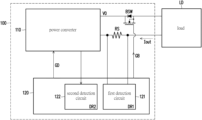
- FIG. 1 is a schematic view of a power supply device according to the first embodiment of the disclosure.
- FIG. 2 is a schematic view of a power supply device according to the second embodiment of the disclosure.
- FIG. 3 is a schematic view of a power supply device according to the third embodiment of the disclosure.
- FIG. 4 is a schematic view of a power supply device according to the fourth embodiment of the disclosure.
- FIG. 5 is a schematic view of the power supply device supplying power to a load through a Type-C communication cable according to the first embodiment.
- FIG. 1 is a schematic view of a power supply device according to the first embodiment of the disclosure.
- a power supply device 100 includes a power converter 110 and a controller 120 .
- the controller 120 is coupled to the power converter 110 .
- the controller 120 controls the power converter 110 to generate an output power VO.
- the controller 120 provides a control signal GD.
- the power converter 110 generates the output power VO in response to the control signal GD.
- the power supply device 100 outputs the output power VO to a load LD.
- the controller 120 includes a first detection circuit 121 and a second detection circuit 122 .
- the first detection circuit 121 detects the output power VO to obtain a first detection result DR 1 .
- the first detection result DR 1 is a variation of an output current value of the output power VO.
- the power supply device 100 further includes a detection resistor RS.
- the detection resistor RS is coupled between an output terminal of the power converter 110 and the load LD.
- An output current Iout of the output power VO flows through the detection resistor RS. Therefore, a voltage difference corresponding to the output current Iout is generated at two terminals of the detection resistor RS.
- the first detection circuit 121 detects the voltage difference at the two terminals of the detection resistor RS, and obtains the first detection result DR 1 corresponding to the output current value based on the voltage difference at the two terminals of the detection resistor RS.
- the first detection circuit 121 provides a precise detection method.
- the first detection result DR 1 is equal to the variation of the output current value. Therefore, the controller 120 controls the power converter 110 in response to the first detection result DR 1 , so that the power supply device 100 complies with a safety standard (e.g., the safety standard IEC 60950).
- the controller 120 controls the power converter 110 in response to the first detection result DR 1 , so that the power supply device 100 complies with limited power source (LPS) requirements of the safety standard IEC 60950.
- LPS limited power source
- the power supply device 100 does not need to provide a fire enclosure, but may use a relatively inexpensive enclosure material with a HB flammability rate. Therefore, the cost of the power supply device 100 may be reduced while complying with the LPS requirements.
- the second detection circuit 122 detects electrical characteristics other than the output current value to obtain a second detection result DR 2 .
- the controller 120 determines whether to limit output of the output power VO according to a relationship between the first detection result DR 1 and the second detection result DR 2 . Taking this embodiment as an example, the controller 120 determines whether to stop the power supply device 100 from supplying the output power VO to the load LD according to the relationship between the first detection result DR 1 and the second detection result DR 2 .
- the controller 120 determines whether to reduce a voltage or a current of the output power VO according to the relationship between the first detection result DR 1 and the second detection result DR 2 .
- the second detection result DR 2 is a variation of the electrical characteristics other than the output current value. However, a trend of the variation of the second detection result DR 2 is still positively correlated or negatively correlated with the variation of the output current value.
- the controller 120 determines whether to limit the output of the output power VO according to the correlation between the first detection result DR 1 and the second detection result DR 2 . For example, when the detection resistor RS is shorted, the variation does not occur in the first detection result DR 1 does not vary. However, the variation occurs in the second detection result DR 2 . That is, the second detection result DR 2 is independent of the first detection result DR 1 . Therefore, when the load LD may continuously receive the output power VO, the controller 120 determines that a first detection method has been invalid. The controller 120 enables the power supply device 100 to limit the output of the output power VO.
- the controller 120 determines whether to enable the power supply device 100 to limit the output of the output power VO according to the relationship between the first detection result DR 1 and the second detection result DR 2 , for example, to stop the power supply device 100 from supplying the output power VO to the load LD.
- the controller 120 may determine whether detection of the first detection circuit 121 is invalid according to the second detection result DR 2 .
- the power supply device 100 limits the output of the output power VO. In this way, the power supply device 100 may avoid misoperation and/or safety hazards when the detection of the first detection circuit 121 is invalid.
- the power supply device 100 further includes a blocking switch BSW.
- a first terminal of the blocking switch BSW is coupled to the output terminal of the power converter 110 .
- a second terminal of the blocking switch BSW is coupled to the load LD.
- a control terminal of the blocking switch BSW is coupled to the controller 120 .
- the controller 120 turns on the blocking switch BSW to enable the power supply device 100 to supply the output power VO to the load LD.
- the controller 120 turns off the blocking switch BSW to enable the power supply device 100 to stop supplying the output power VO to the load LD.
- the controller 120 when the detection of the first detection circuit 121 is determined to be normal, the controller 120 provides a control signal GB having a first voltage level (e.g., a high voltage level) to turn on the blocking switch BSW. Therefore, the power supply device 100 supplies the output power VO to the load LD.
- the controller 120 when the detection of the first detection circuit 121 is determined to be invalid, the controller 120 provides the control signal GB having a second voltage level (e.g., a low voltage level) to turn off the blocking switch BSW. Therefore, the power supply device 100 does not supply the output power VO to the load LD.
- the power converter 110 may be implemented by a flyback power converter, a boost converter, a buck converter, an LLC resonant power converter, an asymmetrical half-bridge (AHB) power converter, or one or any combination of other types of converters.
- the load LD may be an electronic device or an electrical appliance.
- the second detection circuit 122 may obtain at least one second detection result DR 2 through at least one detection method.
- possible methods to obtain the second detection result DR 2 will be exemplified in several embodiments.
- FIG. 2 is a schematic view of a power supply device according to the second embodiment of the disclosure.
- a power supply device 200 includes a power converter 210 , a controller 220 , the blocking switch BSW, and the detection resistor RS.
- the power converter 210 includes a primary side and a secondary side.
- the power converter 210 includes an optocoupler 211 .
- the optocoupler 211 includes a light emitting diode D and a phototransistor T.
- an anode of the light emitting diode D is coupled to an output terminal of the power converter 210 .
- a cathode of the light emitting diode D is coupled to the controller 220 .
- the disclosure is not limited thereto.
- the secondary side of the power converter 210 includes an output diode DO and an output condenser CO.
- a cathode of the output diode DO is used as the output terminal of the power converter 210 .
- a first terminal of the output condenser CO is coupled to the cathode of the output diode DO.
- a second terminal of the output condenser CO is coupled to a ground terminal GND 1 .
- the first terminal of the blocking switch BSW is coupled to the cathode of the diode.
- the detection resistor RS is coupled between the second terminal of the output condenser CO and the load LD.
- a first terminal of the phototransistor T is coupled to a voltage source VB.
- a second terminal of the phototransistor T is coupled to a ground terminal GND 2 .
- the voltage source VB may be provided by a primary-side controller (not shown) on the same side as the phototransistor T.
- the first terminal of the phototransistor T is coupled to a connected node FB.
- the ground terminal GND 2 is different from the ground terminal GND 1 .
- the controller 220 may, for example, receive the output power VO, and adjust a voltage value at the cathode of the light emitting diode D based on the variation of the output power VO.
- the output current value of the output power VO is correlated with a current value flowing through the light emitting diode D. Therefore, the variation of the output current value of the output power VO changes a turn-on current of the phototransistor T, thereby affecting a voltage level of the connected node FB or charge and discharge conditions.
- the controller 220 stabilizes the output power VO according to the voltage level of the connected node FB or the charge and discharge conditions.
- the power converter 210 includes a power switch. The power switch performs a switching operation based on a control signal provided by the controller 220 . The controller 220 adjusts a frequency or a duty cycle of the control signal according to the voltage level of the connected node FB or the charge and discharge conditions, thereby stabilizing the output power VO.
- a resistor R 1 may be provided to limit the current value flowing through the light emitting diode D.
- a resistor R 2 may be provided to limit a current value flowing through the phototransistor T.
- the controller 220 includes a first detection circuit 221 and a second detection circuit 222 .
- a detection operation of the first detection circuit 221 is substantially similar to a detection operation of the first detection circuit 121 in the first embodiment. Therefore, the same details will not be repeated in the following.
- the output current value of the output power VO is correlated with the current value flowing through the light emitting diode D.
- the current value flowing through the light emitting diode D is smaller. Therefore, the second detection circuit 222 detects the current value flowing through the light emitting diode.
- the second detection result DR 2 is a variation of the current value flowing through the light emitting diode D.
- the controller 220 controls the power supply device 200 to limit the output of the output power VO.
- a first threshold and a second threshold are provided, and the second threshold is greater than the first threshold.
- the controller 220 controls the power supply device 200 to limit the output of the output power VO.
- the controller 220 enables the power supply device 200 to supply the output power VO to the load LD.
- FIG. 3 is a schematic view of a power supply device according to the third embodiment of the disclosure.
- a power supply device 300 includes a power converter 310 , a controller 320 , the blocking switch BSW, and the detection resistor RS.
- the power converter 310 includes a synchronous rectifying switch SRSW and the output condenser CO.
- a terminal of the synchronous rectifying switch SRSW is coupled to the first terminal of the output condenser CO as an output terminal (in which the disclosure is not limited thereto).
- the synchronous rectifying switch SRSW performs a synchronous rectifying operation in response to a control signal GSR.
- the controller 320 includes a first detection circuit 321 and a second detection circuit 322 .
- a detection operation of the first detection circuit 321 is substantially similar to the detection operation of the first detection circuit 121 in the first embodiment. Therefore, the same details will not be repeated in the following.
- the second detection circuit 322 detects time that the synchronous rectifying switch SRSW is turned on. Therefore, the second detection result DR 2 is a variation of the time that the synchronous rectifying switch SRSW is turned on. Furthermore, the controller 320 further includes a driver 323 .
- the driver 323 provides the control signal GSR having the duty cycle.
- the second detection circuit 322 receives and detects the control signal GSR, and obtains the time that the synchronous rectifying switch SRSW is turned on according to the duty cycle of the control signal GSR. The time that the synchronous rectifying switch SRSW is turned on is positively correlated with the output current value.
- the first threshold and the second threshold are provided, and the second threshold is greater than the first threshold.
- the variation of the first detection result DR 1 is less than the first threshold, and the variation of the time that the synchronous rectifying switch SRSW is turned on is greater than the second threshold, it indicates that the second detection result DR 2 has the significant variation, while the first detection result DR 1 has the extremely small variation (or no variation).
- the trends of the second detection result DR 2 and the first detection result DR 1 are not consistent. For example, when the detection resistor RS is shorted or opened, the first detection result DR 1 indicates that the output current value is equal to 0 ampere.
- the second detection result DR indicates that the duty cycle of the control signal GSR is greater than a threshold (for example, 10% or 20%, and the disclosure is not limited thereto).
- a threshold for example, 10% or 20%, and the disclosure is not limited thereto.
- the controller 320 controls the power supply device 300 to limit the output of the output power VO.
- the second detection result DR 2 is negatively correlated with the first detection result DR 1 , it indicates that the second detection result DR 2 and the first detection result DR 1 are contradictory.
- the controller 320 controls the power supply device 300 to limit the output of the output power source VO.
- the controller 320 enables the power supply device 300 to supply the output power VO to the load LD.
- FIG. 4 is a schematic view of a power supply device according to the fourth embodiment of the disclosure.
- a power supply device 400 includes a power converter 410 , a controller 420 , the blocking switch BSW, and the detection resistor RS.
- the controller 420 includes a first detection circuit 421 and a second detection circuit 422 .
- a detection operation of the first detection circuit 421 is substantially similar to the detection operation of the first detection circuit 121 in the first embodiment. Therefore, the same details will not be repeated in the following.
- the second detection circuit 422 detects a turn-on voltage value of the blocking switch BSW. Furthermore, the second detection circuit 422 obtains in advance the turn-on voltage value of the blocking switch BSW in a turn-on state. When the blocking switch BSW is in the turn-on state, the second detection circuit 422 receives a voltage difference between the first terminal of the blocking switch BSW and the second terminal of the blocking switch BSW, and divides the voltage difference by the turn-on voltage value to obtain the turn-on voltage value of the blocking switch BSW. The turn-on voltage value of the blocking switch BSW is positively correlated with the output current value. Therefore, the second detection result DR 2 is a variation of the turn-on voltage value.
- the first threshold and the second threshold are provided, and the second threshold is greater than the first threshold.
- the variation of the first detection result DR 1 is less than the first threshold, and the variation of the turn-on voltage value is greater than the second threshold, it indicates that the second detection result DR 2 has the significant variation, while the first detection result DR 1 has the extremely small variation (or no variation).
- the trends of the second detection result DR 2 and the first detection result DR 1 are not consistent.
- the controller 420 controls the power supply device 400 to control.
- the controller 420 controls the power supply device 400 to control.
- the controller 420 enables the power supply device 400 to supply the output power VO to the load LD.
- FIG. 5 is a schematic view of the power supply device supplying power to a load through a Type-C communication cable according to the first embodiment.
- the power supply device 100 further supplies power to the load LD through a communication cable CB complying with the Type-C protocol.
- the communication cable CB includes a power channel Vbus, a configuration channel CC, and a ground channel CGND.
- the configuration channel CC is coupled between a configuration channel pin P 1 of the power supply device 100 and a configuration channel pin P 4 of the load LD.
- the ground channel CGND is coupled between a ground channel pin P 2 of the power supply device 100 and a ground pin P 5 of the load LD.
- the power channel Vbus is coupled between a power pin P 3 of the power supply device 100 and a power pin P 6 of the load LD.
- the power supply device 100 further includes a current source Ip or an equivalent circuit.
- the current source Ip is configured to provide a constant current signal to the load LD.
- a pull-down resistor Rd of the load LD establishes a voltage difference VR at two terminals of the pull-down resistor Rd according to the constant current signal.
- the load LD and the power supply device 100 determine whether to perform communication or to supply and output the output power VO in response to the voltage difference VR at the two terminals of the pull-down resistor Rd.
- the second detection circuit 122 detects a voltage difference VD between the configuration channel pin P 1 and the ground channel pin P 2 of the power converter 110 . Furthermore, the controller 320 may obtain the voltage difference VD between the configuration channel pin P 1 and the ground channel pin P 2 according to Formula (1). VD ⁇ ( i _ I out+ i _ Ip ) ⁇ r _ Rc+i _ Ip ⁇ r _ Rd Formula (1)
- i_Iout is represented as a current value of the output current Iout
- r_Rc is represented as a resistance value of an equivalent path resistance Rc on a transmission path of the output current Iout
- i_Ip is represented as a current value of the constant current signal
- r_Rd is represented as a resistance value of the pull-down resistor Rd.
- the transmission path includes the power channel Vbus, a current path CP inside the load LD, and the configuration channel CC.
- the equivalent path resistance Rc in this embodiment is shown in configuration channel CC as an example.
- the current value of the constant current signal is significantly less than the current value of the output current Iout.
- the resistance value of the equivalent path resistance Rc is significantly less than the resistance value of the pull-down resistor Rd.
- Formula (1) may be simplified to Formula (2).
- the controller 320 may obtain the voltage difference VR at the two terminals of the pull-down resistor Rd according to Formula (3).
- VR i _ Ip ⁇ r _ Rd Formula (3)
- the voltage difference VR at the two terminals of the pull-down resistor Rd is equal to a product of the current value of the constant current signal and the resistance value of the pull-down resistor Rd.
- the voltage difference VR is a constant value. Therefore, based on Formulas (2) and (3), the voltage difference VD between the configuration channel pin P 1 and the ground channel pin P 2 is proportional to the current value of the output current Iout. Therefore, the second detection result DR 2 of the second detection circuit 122 is a variation of the voltage difference VD.
- the first threshold and the second threshold are provided, and the second threshold is greater than the first threshold.
- the controller 320 controls the power supply device 300 to limit the output of the output power source VO.
- the controller 320 controls the power supply device 300 to limit the output of the output power source VO.
- the controller 320 enables the power supply device 300 to supply the output power VO to the load LD.
- the controller 320 may accurately obtain the current value of the output current Iout according to Formula (4).
- the first detection circuit in the disclosure detects the output power to obtain the precise first detection result.
- the second detection circuit detects the electrical characteristics other than the output current value to obtain the second detection result.
- the controller may determine whether the detection of the first detection circuit is invalid according to the second detection result. When the detection of the first detection circuit is determined to be invalid, the controller controls the power supply device to limit the output of the output power source VO.
- the power supply device in the disclosure may avoid the misoperation and/or the safety hazards that may occur when the first detection result is invalid.
Landscapes
- Engineering & Computer Science (AREA)
- Power Engineering (AREA)
- Physics & Mathematics (AREA)
- General Physics & Mathematics (AREA)
- Dc-Dc Converters (AREA)
- Heat-Pump Type And Storage Water Heaters (AREA)
- Apparatus For Radiation Diagnosis (AREA)
Applications Claiming Priority (2)
| Application Number | Priority Date | Filing Date | Title |
|---|---|---|---|
| TW110149269 | 2021-12-29 | ||
| TW110149269A TWI808584B (zh) | 2021-12-29 | 2021-12-29 | 電源供應裝置 |
Publications (2)
| Publication Number | Publication Date |
|---|---|
| US20230209678A1 US20230209678A1 (en) | 2023-06-29 |
| US11930573B2 true US11930573B2 (en) | 2024-03-12 |
Family
ID=86896598
Family Applications (1)
| Application Number | Title | Priority Date | Filing Date |
|---|---|---|---|
| US17/960,140 Active US11930573B2 (en) | 2021-12-29 | 2022-10-05 | Power supply device |
Country Status (3)
| Country | Link |
|---|---|
| US (1) | US11930573B2 (zh) |
| CN (1) | CN116418228A (zh) |
| TW (1) | TWI808584B (zh) |
Citations (2)
| Publication number | Priority date | Publication date | Assignee | Title |
|---|---|---|---|---|
| US9742293B2 (en) * | 2016-01-21 | 2017-08-22 | Inno-Tech Co., Ltd. | Power supply and method of power supplying |
| US20180241308A1 (en) * | 2015-02-16 | 2018-08-23 | Tdk Corporation | Control circuit and switching power supply |
Family Cites Families (4)
| Publication number | Priority date | Publication date | Assignee | Title |
|---|---|---|---|---|
| US7764516B2 (en) * | 2008-02-21 | 2010-07-27 | System General Corporation | Method and apparatus of providing synchronous regulation circuit for offline power converter |
| TWI498704B (zh) * | 2012-11-06 | 2015-09-01 | 泰達電子公司 | 可動態調整輸出電壓之電源轉換器及其適用之供電系統 |
| TWI523392B (zh) * | 2013-10-30 | 2016-02-21 | 南京博蘭得電子科技有限公司 | 諧振變換器及其控制方法 |
| TWI719573B (zh) * | 2019-08-06 | 2021-02-21 | 台達電子工業股份有限公司 | 電源轉換器及電源轉換器的控制方法 |
-
2021
- 2021-12-29 TW TW110149269A patent/TWI808584B/zh active
-
2022
- 2022-02-10 CN CN202210125126.6A patent/CN116418228A/zh active Pending
- 2022-10-05 US US17/960,140 patent/US11930573B2/en active Active
Patent Citations (2)
| Publication number | Priority date | Publication date | Assignee | Title |
|---|---|---|---|---|
| US20180241308A1 (en) * | 2015-02-16 | 2018-08-23 | Tdk Corporation | Control circuit and switching power supply |
| US9742293B2 (en) * | 2016-01-21 | 2017-08-22 | Inno-Tech Co., Ltd. | Power supply and method of power supplying |
Also Published As
| Publication number | Publication date |
|---|---|
| CN116418228A (zh) | 2023-07-11 |
| TWI808584B (zh) | 2023-07-11 |
| TW202326338A (zh) | 2023-07-01 |
| US20230209678A1 (en) | 2023-06-29 |
Similar Documents
| Publication | Publication Date | Title |
|---|---|---|
| US10337676B2 (en) | LED tube lamp | |
| US20190006949A1 (en) | Isolated synchronous rectification-type dc/dc converter | |
| US8508151B2 (en) | Power unit and lighting apparatus | |
| US10277133B2 (en) | Isolated DC/DC converter, primary side controller, power adapter, and electronic device | |
| US20160118900A1 (en) | Power supply adaptor | |
| US9763295B2 (en) | Switching converter and lighting device using the same | |
| US20120147631A1 (en) | Dc/dc converter, and power supply and electronic device using the same | |
| US20060209581A1 (en) | Terminal for multiple functions in a power supply | |
| US20120181952A1 (en) | Drive circuit for light-emmiting diode array | |
| JP6554321B2 (ja) | 絶縁同期整流型dc/dcコンバータおよびその同期整流コントローラ、それを用いた電源装置、電源アダプタおよび電子機器 | |
| KR20120081610A (ko) | Led 드라이버의 디밍 | |
| TW201539914A (zh) | 電源供應裝置 | |
| WO2017075296A1 (en) | Wall mounted ac to dc converter gang box | |
| JP6707390B2 (ja) | 絶縁型のdc/dcコンバータ、それを用いた電源アダプタおよび電子機器、その制御方法 | |
| JP5595255B2 (ja) | Led電源装置 | |
| US6940233B2 (en) | Method and system of driving a CCFL | |
| US10389256B2 (en) | Isolated DC/DC converter and primary side controller thereof, control method and power adaptor and electronic device using the same | |
| CN101868105B (zh) | 一种电子镇流器及其过压保护方法 | |
| US11930573B2 (en) | Power supply device | |
| TWI751518B (zh) | 支援電力輸送之充電裝置 | |
| US9584033B1 (en) | Power supply device for varying an output voltage | |
| US11915628B2 (en) | Display device including overload protection circuit | |
| KR20090018605A (ko) | 교류 전원 장치 및 교류 전원 장치용 집적 회로 | |
| CN109640437B (zh) | 一种led调光控制系统 | |
| CN220570463U (zh) | 一种负载可调电路、电源电路、电路板及电子设备 |
Legal Events
| Date | Code | Title | Description |
|---|---|---|---|
| FEPP | Fee payment procedure |
Free format text: ENTITY STATUS SET TO UNDISCOUNTED (ORIGINAL EVENT CODE: BIG.); ENTITY STATUS OF PATENT OWNER: LARGE ENTITY |
|
| AS | Assignment |
Owner name: POWER FOREST TECHNOLOGY CORPORATION, TAIWAN Free format text: ASSIGNMENT OF ASSIGNORS INTEREST;ASSIGNORS:TU, RONG-JIE;CHIU, HUNG-CHIH;LEE, CHIEN-LUNG;SIGNING DATES FROM 20220330 TO 20220912;REEL/FRAME:061447/0005 |
|
| STPP | Information on status: patent application and granting procedure in general |
Free format text: DOCKETED NEW CASE - READY FOR EXAMINATION |
|
| STPP | Information on status: patent application and granting procedure in general |
Free format text: NON FINAL ACTION MAILED |
|
| STPP | Information on status: patent application and granting procedure in general |
Free format text: RESPONSE TO NON-FINAL OFFICE ACTION ENTERED AND FORWARDED TO EXAMINER |
|
| STPP | Information on status: patent application and granting procedure in general |
Free format text: NOTICE OF ALLOWANCE MAILED -- APPLICATION RECEIVED IN OFFICE OF PUBLICATIONS |
|
| STPP | Information on status: patent application and granting procedure in general |
Free format text: PUBLICATIONS -- ISSUE FEE PAYMENT VERIFIED |
|
| STCF | Information on status: patent grant |
Free format text: PATENTED CASE |