US11929354B2 - Power semiconductor module - Google Patents
Power semiconductor module Download PDFInfo
- Publication number
- US11929354B2 US11929354B2 US17/134,646 US202017134646A US11929354B2 US 11929354 B2 US11929354 B2 US 11929354B2 US 202017134646 A US202017134646 A US 202017134646A US 11929354 B2 US11929354 B2 US 11929354B2
- Authority
- US
- United States
- Prior art keywords
- power semiconductor
- corrosion
- wiring member
- corrosion sensor
- semiconductor module
- Prior art date
- Legal status (The legal status is an assumption and is not a legal conclusion. Google has not performed a legal analysis and makes no representation as to the accuracy of the status listed.)
- Active, expires
Links
Images


Classifications
-
- H—ELECTRICITY
- H01—ELECTRIC ELEMENTS
- H01L—SEMICONDUCTOR DEVICES NOT COVERED BY CLASS H10
- H01L25/00—Assemblies consisting of a plurality of semiconductor or other solid state devices
- H01L25/03—Assemblies consisting of a plurality of semiconductor or other solid state devices all the devices being of a type provided for in a single subclass of subclasses H10B, H10D, H10F, H10H, H10K or H10N, e.g. assemblies of rectifier diodes
- H01L25/04—Assemblies consisting of a plurality of semiconductor or other solid state devices all the devices being of a type provided for in a single subclass of subclasses H10B, H10D, H10F, H10H, H10K or H10N, e.g. assemblies of rectifier diodes the devices not having separate containers
- H01L25/075—Assemblies consisting of a plurality of semiconductor or other solid state devices all the devices being of a type provided for in a single subclass of subclasses H10B, H10D, H10F, H10H, H10K or H10N, e.g. assemblies of rectifier diodes the devices not having separate containers the devices being of a type provided for in group H10H20/00
- H01L25/0753—Assemblies consisting of a plurality of semiconductor or other solid state devices all the devices being of a type provided for in a single subclass of subclasses H10B, H10D, H10F, H10H, H10K or H10N, e.g. assemblies of rectifier diodes the devices not having separate containers the devices being of a type provided for in group H10H20/00 the devices being arranged next to each other
-
- H—ELECTRICITY
- H02—GENERATION; CONVERSION OR DISTRIBUTION OF ELECTRIC POWER
- H02M—APPARATUS FOR CONVERSION BETWEEN AC AND AC, BETWEEN AC AND DC, OR BETWEEN DC AND DC, AND FOR USE WITH MAINS OR SIMILAR POWER SUPPLY SYSTEMS; CONVERSION OF DC OR AC INPUT POWER INTO SURGE OUTPUT POWER; CONTROL OR REGULATION THEREOF
- H02M1/00—Details of apparatus for conversion
- H02M1/32—Means for protecting converters other than automatic disconnection
-
- G—PHYSICS
- G01—MEASURING; TESTING
- G01K—MEASURING TEMPERATURE; MEASURING QUANTITY OF HEAT; THERMALLY-SENSITIVE ELEMENTS NOT OTHERWISE PROVIDED FOR
- G01K7/00—Measuring temperature based on the use of electric or magnetic elements directly sensitive to heat ; Power supply therefor, e.g. using thermoelectric elements
- G01K7/01—Measuring temperature based on the use of electric or magnetic elements directly sensitive to heat ; Power supply therefor, e.g. using thermoelectric elements using semiconducting elements having PN junctions
-
- G—PHYSICS
- G01—MEASURING; TESTING
- G01N—INVESTIGATING OR ANALYSING MATERIALS BY DETERMINING THEIR CHEMICAL OR PHYSICAL PROPERTIES
- G01N17/00—Investigating resistance of materials to the weather, to corrosion, or to light
- G01N17/04—Corrosion probes
-
- H—ELECTRICITY
- H01—ELECTRIC ELEMENTS
- H01L—SEMICONDUCTOR DEVICES NOT COVERED BY CLASS H10
- H01L24/00—Arrangements for connecting or disconnecting semiconductor or solid-state bodies; Methods or apparatus related thereto
- H01L24/01—Means for bonding being attached to, or being formed on, the surface to be connected, e.g. chip-to-package, die-attach, "first-level" interconnects; Manufacturing methods related thereto
- H01L24/26—Layer connectors, e.g. plate connectors, solder or adhesive layers; Manufacturing methods related thereto
- H01L24/31—Structure, shape, material or disposition of the layer connectors after the connecting process
- H01L24/32—Structure, shape, material or disposition of the layer connectors after the connecting process of an individual layer connector
-
- H—ELECTRICITY
- H01—ELECTRIC ELEMENTS
- H01L—SEMICONDUCTOR DEVICES NOT COVERED BY CLASS H10
- H01L24/00—Arrangements for connecting or disconnecting semiconductor or solid-state bodies; Methods or apparatus related thereto
- H01L24/01—Means for bonding being attached to, or being formed on, the surface to be connected, e.g. chip-to-package, die-attach, "first-level" interconnects; Manufacturing methods related thereto
- H01L24/42—Wire connectors; Manufacturing methods related thereto
- H01L24/47—Structure, shape, material or disposition of the wire connectors after the connecting process
- H01L24/48—Structure, shape, material or disposition of the wire connectors after the connecting process of an individual wire connector
-
- H—ELECTRICITY
- H01—ELECTRIC ELEMENTS
- H01L—SEMICONDUCTOR DEVICES NOT COVERED BY CLASS H10
- H01L24/00—Arrangements for connecting or disconnecting semiconductor or solid-state bodies; Methods or apparatus related thereto
- H01L24/73—Means for bonding being of different types provided for in two or more of groups H01L24/10, H01L24/18, H01L24/26, H01L24/34, H01L24/42, H01L24/50, H01L24/63, H01L24/71
-
- H—ELECTRICITY
- H01—ELECTRIC ELEMENTS
- H01L—SEMICONDUCTOR DEVICES NOT COVERED BY CLASS H10
- H01L25/00—Assemblies consisting of a plurality of semiconductor or other solid state devices
- H01L25/18—Assemblies consisting of a plurality of semiconductor or other solid state devices the devices being of the types provided for in two or more different main groups of the same subclass of H10B, H10D, H10F, H10H, H10K or H10N
-
- H—ELECTRICITY
- H02—GENERATION; CONVERSION OR DISTRIBUTION OF ELECTRIC POWER
- H02M—APPARATUS FOR CONVERSION BETWEEN AC AND AC, BETWEEN AC AND DC, OR BETWEEN DC AND DC, AND FOR USE WITH MAINS OR SIMILAR POWER SUPPLY SYSTEMS; CONVERSION OF DC OR AC INPUT POWER INTO SURGE OUTPUT POWER; CONTROL OR REGULATION THEREOF
- H02M7/00—Conversion of AC power input into DC power output; Conversion of DC power input into AC power output
- H02M7/003—Constructional details, e.g. physical layout, assembly, wiring or busbar connections
-
- H—ELECTRICITY
- H02—GENERATION; CONVERSION OR DISTRIBUTION OF ELECTRIC POWER
- H02M—APPARATUS FOR CONVERSION BETWEEN AC AND AC, BETWEEN AC AND DC, OR BETWEEN DC AND DC, AND FOR USE WITH MAINS OR SIMILAR POWER SUPPLY SYSTEMS; CONVERSION OF DC OR AC INPUT POWER INTO SURGE OUTPUT POWER; CONTROL OR REGULATION THEREOF
- H02M7/00—Conversion of AC power input into DC power output; Conversion of DC power input into AC power output
- H02M7/42—Conversion of DC power input into AC power output without possibility of reversal
- H02M7/44—Conversion of DC power input into AC power output without possibility of reversal by static converters
- H02M7/48—Conversion of DC power input into AC power output without possibility of reversal by static converters using discharge tubes with control electrode or semiconductor devices with control electrode
- H02M7/53—Conversion of DC power input into AC power output without possibility of reversal by static converters using discharge tubes with control electrode or semiconductor devices with control electrode using devices of a triode or transistor type requiring continuous application of a control signal
- H02M7/537—Conversion of DC power input into AC power output without possibility of reversal by static converters using discharge tubes with control electrode or semiconductor devices with control electrode using devices of a triode or transistor type requiring continuous application of a control signal using semiconductor devices only, e.g. single switched pulse inverters
- H02M7/5387—Conversion of DC power input into AC power output without possibility of reversal by static converters using discharge tubes with control electrode or semiconductor devices with control electrode using devices of a triode or transistor type requiring continuous application of a control signal using semiconductor devices only, e.g. single switched pulse inverters in a bridge configuration
- H02M7/53871—Conversion of DC power input into AC power output without possibility of reversal by static converters using discharge tubes with control electrode or semiconductor devices with control electrode using devices of a triode or transistor type requiring continuous application of a control signal using semiconductor devices only, e.g. single switched pulse inverters in a bridge configuration with automatic control of output voltage or current
-
- H10W90/00—
-
- G—PHYSICS
- G01—MEASURING; TESTING
- G01K—MEASURING TEMPERATURE; MEASURING QUANTITY OF HEAT; THERMALLY-SENSITIVE ELEMENTS NOT OTHERWISE PROVIDED FOR
- G01K13/00—Thermometers specially adapted for specific purposes
-
- H—ELECTRICITY
- H01—ELECTRIC ELEMENTS
- H01L—SEMICONDUCTOR DEVICES NOT COVERED BY CLASS H10
- H01L2224/00—Indexing scheme for arrangements for connecting or disconnecting semiconductor or solid-state bodies and methods related thereto as covered by H01L24/00
- H01L2224/01—Means for bonding being attached to, or being formed on, the surface to be connected, e.g. chip-to-package, die-attach, "first-level" interconnects; Manufacturing methods related thereto
- H01L2224/26—Layer connectors, e.g. plate connectors, solder or adhesive layers; Manufacturing methods related thereto
- H01L2224/31—Structure, shape, material or disposition of the layer connectors after the connecting process
- H01L2224/32—Structure, shape, material or disposition of the layer connectors after the connecting process of an individual layer connector
- H01L2224/321—Disposition
- H01L2224/32151—Disposition the layer connector connecting between a semiconductor or solid-state body and an item not being a semiconductor or solid-state body, e.g. chip-to-substrate, chip-to-passive
- H01L2224/32221—Disposition the layer connector connecting between a semiconductor or solid-state body and an item not being a semiconductor or solid-state body, e.g. chip-to-substrate, chip-to-passive the body and the item being stacked
- H01L2224/32225—Disposition the layer connector connecting between a semiconductor or solid-state body and an item not being a semiconductor or solid-state body, e.g. chip-to-substrate, chip-to-passive the body and the item being stacked the item being non-metallic, e.g. insulating substrate with or without metallisation
-
- H—ELECTRICITY
- H01—ELECTRIC ELEMENTS
- H01L—SEMICONDUCTOR DEVICES NOT COVERED BY CLASS H10
- H01L2224/00—Indexing scheme for arrangements for connecting or disconnecting semiconductor or solid-state bodies and methods related thereto as covered by H01L24/00
- H01L2224/01—Means for bonding being attached to, or being formed on, the surface to be connected, e.g. chip-to-package, die-attach, "first-level" interconnects; Manufacturing methods related thereto
- H01L2224/42—Wire connectors; Manufacturing methods related thereto
- H01L2224/47—Structure, shape, material or disposition of the wire connectors after the connecting process
- H01L2224/48—Structure, shape, material or disposition of the wire connectors after the connecting process of an individual wire connector
- H01L2224/481—Disposition
- H01L2224/48151—Connecting between a semiconductor or solid-state body and an item not being a semiconductor or solid-state body, e.g. chip-to-substrate, chip-to-passive
- H01L2224/48221—Connecting between a semiconductor or solid-state body and an item not being a semiconductor or solid-state body, e.g. chip-to-substrate, chip-to-passive the body and the item being stacked
- H01L2224/48225—Connecting between a semiconductor or solid-state body and an item not being a semiconductor or solid-state body, e.g. chip-to-substrate, chip-to-passive the body and the item being stacked the item being non-metallic, e.g. insulating substrate with or without metallisation
- H01L2224/48227—Connecting between a semiconductor or solid-state body and an item not being a semiconductor or solid-state body, e.g. chip-to-substrate, chip-to-passive the body and the item being stacked the item being non-metallic, e.g. insulating substrate with or without metallisation connecting the wire to a bond pad of the item
-
- H—ELECTRICITY
- H01—ELECTRIC ELEMENTS
- H01L—SEMICONDUCTOR DEVICES NOT COVERED BY CLASS H10
- H01L2224/00—Indexing scheme for arrangements for connecting or disconnecting semiconductor or solid-state bodies and methods related thereto as covered by H01L24/00
- H01L2224/73—Means for bonding being of different types provided for in two or more of groups H01L2224/10, H01L2224/18, H01L2224/26, H01L2224/34, H01L2224/42, H01L2224/50, H01L2224/63, H01L2224/71
- H01L2224/732—Location after the connecting process
- H01L2224/73251—Location after the connecting process on different surfaces
- H01L2224/73265—Layer and wire connectors
-
- H—ELECTRICITY
- H01—ELECTRIC ELEMENTS
- H01L—SEMICONDUCTOR DEVICES NOT COVERED BY CLASS H10
- H01L2924/00—Indexing scheme for arrangements or methods for connecting or disconnecting semiconductor or solid-state bodies as covered by H01L24/00
- H01L2924/10—Details of semiconductor or other solid state devices to be connected
- H01L2924/11—Device type
- H01L2924/12—Passive devices, e.g. 2 terminal devices
- H01L2924/1203—Rectifying Diode
-
- H—ELECTRICITY
- H01—ELECTRIC ELEMENTS
- H01L—SEMICONDUCTOR DEVICES NOT COVERED BY CLASS H10
- H01L2924/00—Indexing scheme for arrangements or methods for connecting or disconnecting semiconductor or solid-state bodies as covered by H01L24/00
- H01L2924/10—Details of semiconductor or other solid state devices to be connected
- H01L2924/11—Device type
- H01L2924/13—Discrete devices, e.g. 3 terminal devices
- H01L2924/1304—Transistor
- H01L2924/1305—Bipolar Junction Transistor [BJT]
- H01L2924/13055—Insulated gate bipolar transistor [IGBT]
-
- H—ELECTRICITY
- H01—ELECTRIC ELEMENTS
- H01L—SEMICONDUCTOR DEVICES NOT COVERED BY CLASS H10
- H01L2924/00—Indexing scheme for arrangements or methods for connecting or disconnecting semiconductor or solid-state bodies as covered by H01L24/00
- H01L2924/10—Details of semiconductor or other solid state devices to be connected
- H01L2924/11—Device type
- H01L2924/14—Integrated circuits
- H01L2924/141—Analog devices
- H01L2924/1425—Converter
- H01L2924/14252—Voltage converter
-
- H10W72/07552—
-
- H10W72/527—
-
- H10W72/5473—
-
- H10W72/5524—
-
- H10W72/5525—
-
- H10W72/884—
-
- H10W72/926—
-
- H10W90/734—
-
- H10W90/753—
-
- H10W90/754—
Definitions
- the embodiments discussed herein relate to a power semiconductor module.
- power conversion inverter circuits include power semiconductors as switching elements. Insulated gate bipolar transistors (IGBTs) or metal-oxide-semiconductor field-effect transistors (MOSFETs) are generally used as these power semiconductors.
- IGBTs Insulated gate bipolar transistors
- MOSFETs metal-oxide-semiconductor field-effect transistors
- the power semiconductors are incorporated into a single package to constitute a power semiconductor module.
- a power semiconductor module includes one or more power semiconductors.
- These power semiconductor modules have evolved to intelligent power modules (IPMs).
- An IPM includes a drive circuit for driving an individual power semiconductor and a control circuit including peripheral circuits such as various kinds of protection circuits.
- This corrosion sensor for detecting how the corrosion progresses (see, for example, Japanese Laid-open Patent Publication No. 2014-153089).
- This corrosion sensor includes a plurality of series circuits connected in parallel with each other, each of the series circuits being formed by a combination of a metal having a corrosion rate as a calculation target and a fixed resistor.
- This technique calculates how much time it takes for the plurality of metals to be corroded and disconnected in an exposure environment by combining the metals having corrosion rates as the calculation targets based on the resistance values of the corresponding fixed resistors.
- the conventional corrosion sensor needs a plurality of kinds of metals having different corrosion rates, it is difficult to install the corrosion sensor inside a power semiconductor module in view of space. Also, it is difficult to select the installation location.
- a power semiconductor module including: a half-bridge circuit including a first power semiconductor element and a second power semiconductor element that are connected in series with each other; a first external terminal, a second external terminal, and a third external terminal; a first wiring member that connects a high-potential-side main electrode of the first power semiconductor element to the first external terminal; a second wiring member that connects a low-potential-side main electrode of the second power semiconductor element to the second external terminal; a third wiring member that connects an output of the half-bridge circuit to the third external terminal; and at least one of a first corrosion sensor disposed in an installation environment of the first wiring member, a second corrosion sensor disposed in an installation environment of the second wiring member, or a third corrosion sensor disposed in an installation environment of the third wiring member.
- FIG. 1 is a plan view illustrating an example of an internal configuration of a power semiconductor module according to a first embodiment
- FIG. 2 is a circuit diagram of the power semiconductor module according to the first embodiment
- FIG. 3 is a plan view illustrating an example of an internal configuration of a power semiconductor module according to a second embodiment
- FIG. 4 is a circuit diagram of the power semiconductor module according to the second embodiment
- FIG. 5 is a plan view illustrating an example of an internal configuration of a power semiconductor module according to a third embodiment
- FIG. 6 is a circuit diagram of the power semiconductor module according to the third embodiment.
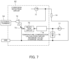
- FIG. 7 is a circuit diagram of a corrosion detection circuit.
- FIG. 1 is a plan view illustrating an example of an internal configuration of a power semiconductor module according to a first embodiment.
- FIG. 2 is a circuit diagram of the power semiconductor module according to the first embodiment.
- this power semiconductor module 10 includes an IGBT 11 , a free wheeling diode (FWD) 12 , and two corrosion sensors 13 and 14 .
- the IGBT 11 and the FWD 12 are mounted on an insulating substrate 15 .
- a circuit pattern 16 is formed on one surface of the insulating substrate 15 , and the IGBT 11 and the FWD 12 are bonded to the circuit pattern 16 via solder.
- the IGBT 11 has a collector terminal, which is a high-potential-side main electrode and is bonded to the circuit pattern 16 via solder.
- the FWD 12 has a cathode terminal bonded to the circuit pattern 16 via solder.
- circuit patterns 17 and 18 are formed on the insulating substrate 15 .
- One terminal of the corrosion sensor 13 is connected to the circuit pattern 17
- one terminal of the corrosion sensor 14 is connected to the circuit pattern 18 .
- This insulating substrate 15 is housed in a case 19 .
- On the frame of the case 19 there are formed a high-potential-side external terminal 20 , a low-potential-side external terminal 21 , external terminals 22 and 23 for inputting control signals, and external terminals 24 to 27 for the corrosion sensors 13 and 14 .
- the high-potential-side external terminal 20 is connected to the circuit pattern 16 via a plurality of bonding wires 28 , which are wiring members.
- bonding wires 28 which are wiring members.
- a main current having a large current capacity is caused to flow through the bonding wires 28 .
- several dozens of bonding wires 28 may be used.
- a single thick line having black circles at both ends represents a plurality of bonding wires.
- the low-potential-side external terminal 21 is connected to the anode terminal of the FWD 12 via a plurality of bonding wires 29 , and the anode terminal of FWD 12 is connected to an emitter terminal of the IGBT 11 , which is a low-potential-side main electrode thereof, via a plurality of bonding wires 30 . In this way, the FWD 12 and the IGBT 11 are connected in reverse parallel with each other.
- the circuit pattern 17 to which one terminal of the corrosion sensor 13 is connected, is connected to the external terminal 24 via a bonding wire 31 , and the other terminal of the corrosion sensor 13 is connected to the external terminal 25 .
- the circuit pattern 18 to which one terminal of the corrosion sensor 14 is connected, is connected to the external terminal 26 via a bonding wire 32 , and the other terminal of the corrosion sensor 14 is connected to the external terminal 27 .
- the external terminal 22 is connected to a gate pad 33 of the IGBT 11 via a bonding wire 34
- the external terminal 23 is connected to the emitter terminal of the IGBT 11 via a bonding wire 35 .
- the corrosion sensor 13 is disposed near the bonding wires 28 through which a main current is inputted, and the corrosion sensor 14 is disposed near the bonding wires 29 through which a main current is outputted.
- the corrosion sensor 13 is disposed in an installation environment of the bonding wire 28 , such as in a vicinity of the bonding wire 28 having a same condition with respect to corrosion of the bonding wire 28 , so as to detect the corrosion of the bonding wire 28 .
- the corrosion sensor 14 is disposed in an installation environment of the bonding wire 29 , such as in a vicinity of the bonding wire 29 having a same condition with respect to corrosion of the bonding wire 29 , so as to detect corrosion of the bonding wire 29 .
- the corrosion sensors 13 and 14 are disposed in high-temperature environments in which heat is generated when the main currents flow through the bonding wires 28 and 29 .
- the corrosion sensors 13 and 14 exhibit corrosion reaction with the bonding wires 28 and 29 .
- the corrosion sensors 13 and 14 use metal resistive wires as resistive elements, and the resistance values of these metal resistive wires rise as the corrosion progresses.
- the material of the metal resistive wires is selected based on the material of the bonding wires 28 and 29 . Namely, when the bonding wires 28 and 29 are made of aluminum, aluminum or an aluminum alloy is used as the material of the metal resistive wires. When the bonding wires 28 and 29 are made of copper, copper or a copper alloy is used as the material of the metal resistive wires.
- the metal resistive wires are formed to have a cross section that achieves a current density higher than that of the bonding wires 28 and 29 . In this way, the resistance values of the metal resistive wires are adjusted to be higher than those of the bonding wires 28 and 29 .
- the corrosion sensors 13 and of this power semiconductor module 10 include metal resistive wires.
- the corrosion sensors 13 and 14 are easily and inexpensively installable even in a small module.
- the corrosion state in the module is determined by the external circuits.
- the external circuits determine the corrosion state in the module by using at least one of the corrosion sensors 13 and 14 , as needed.
- FIG. 3 is a plan view illustrating an example of an internal configuration of a power semiconductor module according to a second embodiment.
- FIG. 4 is a circuit diagram of the power semiconductor module according to the second embodiment.
- the material of the metal resistive wires and the resistance value adjustment method are the same as those according to the first embodiment.
- an individual half-bridge circuit formed by connecting two power semiconductors in series with each other is provided with corrosion sensors 13 and 14 .
- four high-side power semiconductors of the half-bridge circuits are connected in parallel with each other.
- four low-side power semiconductors of the half-bridge circuits are connected in parallel with each other. This connection increases the capacities of the source and sink currents.
- a reverse-conducting IGBT (RC-IGBT) is used as a power semiconductor.
- an IGBT and an FWD are connected to form an individual RC-IGBT as a single element.
- the power semiconductor module 10 a includes eight elements, as illustrated in FIG. 3 .
- This power semiconductor module 10 a includes a high-side insulating substrate 15 a and a low-side insulating substrate 15 b , and these insulating substrates 15 a and 15 b are housed in a case 19 a .
- Circuit patterns 16 a to 16 g are formed on the high-side insulating substrate 15 a
- circuit patterns 16 h to 16 l are formed on the low-side insulating substrate 15 b.
- RC-IGBTs 41 a to 41 d are mounted on the circuit pattern 16 a on the high-side insulating substrate 15 a
- RC-IGBTs 41 e to 41 h are mounted on the circuit pattern 16 h on the low-side insulating substrate 15 b.
- a high-potential-side external terminal 20 , a low-potential-side external terminal 21 , external terminals 24 and 25 for the corrosion sensor 13 , external terminals 26 and 27 for the corrosion sensor 14 , an output external terminal 42 , and external terminals 26 a and 27 a for a corrosion sensor 14 a are formed on the frame of the case 19 a.
- the high-potential-side external terminal 20 is connected to the circuit pattern 16 a via a plurality of bonding wires 28 .
- the emitter terminals of the high-side RC-IGBTs 41 a to 41 d are connected to the circuit pattern 16 b via a plurality of bonding wires 28 a to 28 d .
- the circuit pattern 16 b is connected to the circuit pattern 16 h formed on the low-side insulating substrate 15 b via a plurality of bonding wires 28 e.
- the circuit pattern 16 h is connected to the external terminal 42 via a plurality of bonding wires 28 f .
- the emitter terminals of the low-side RC-IGBTs 41 e to 41 h are connected to the circuit pattern 16 i via a plurality of bonding wires 29 a to 29 d .
- the circuit pattern 16 i is connected to the high-side circuit pattern 16 c via a plurality of bonding wires 29 e
- the circuit pattern 16 c is connected to the low-potential-side external terminal 21 via a plurality of bonding wires 29 .
- the high-side circuit pattern 16 d is connected to gate pads 33 a to 33 d of the high-side RC-IGBTs 41 a to 41 d via bonding wires.
- the circuit pattern 16 e is connected to the emitter terminal of the high-side RC-IGBT 41 b via a bonding wire.
- the low-side circuit pattern 16 j is connected to gate pads 33 e to 33 h of the low-side RC-IGBTs 41 e to 41 h via bonding wires.
- the circuit pattern 16 k is connected to the emitter terminal of the low-side RC-IGBT 41 g via a bonding wire.
- the circuit pattern 16 f to which one terminal of the corrosion sensor 13 is connected, is connected to the external terminal 24 via a bonding wire 31 , and the other terminal of the corrosion sensor 13 is connected to the external terminal 25 .
- the circuit pattern 16 g to which one terminal of the corrosion sensor 14 is connected, is connected to the external terminal 26 via a bonding wire 32 , and the other terminal of the corrosion sensor 14 is connected to the external terminal 27 .
- the circuit pattern 16 l to which one terminal of the corrosion sensor 14 a is connected, is connected to the external terminal 26 a via a bonding wire 32 a , and the other terminal of the corrosion sensor 14 a is connected to the external terminal 27 a.
- the corrosion sensor 13 is disposed near the bonding wire 28 through which a main current is inputted, and the corrosion sensor 14 is disposed near the bonding wire 29 through which a main current is outputted.
- the corrosion sensor 14 a is disposed near the bonding wire 28 f through which a main current is inputted and outputted.
- the corrosion sensor 14 a is disposed in an installation environment of the bonding wire 28 f , such as in a vicinity of the bonding wire 28 f having a same condition of corrosion of the bonding wire 28 f , so as to detect the corrosion of the bonding wire 28 f .
- the corrosion sensors 13 , 14 , and 14 a are disposed in high-temperature environments in which heat is generated when the large currents flow through the bonding wires 28 , 29 , and 28 f .
- the corrosion sensors 13 , 14 , and 14 a exhibit corrosion reaction with the bonding wires 28 , 29 , and 28 f.
- the corrosion sensors 13 , 14 , and 14 a of this power semiconductor module 10 a also have terminals connectable to external circuits. Thus, the corrosion state in the module is determined by observing change in the resistance values of the corrosion sensors 13 , 14 , and 14 a with the external circuits.
- FIG. 5 is a plan view illustrating an example of an internal configuration of a power semiconductor module according to a third embodiment.
- FIG. 6 is a circuit diagram of the power semiconductor module according to the third embodiment.
- FIG. 7 is a circuit diagram of a corrosion detection circuit. The material of the metal resistive wires and the resistance value adjustment method are the same as those according to the first embodiment.
- This power semiconductor module 10 b is an IPM that drives load such as a three-phase motor, and three sets of half-bridge circuits are provided with a corrosion sensor 14 .
- this power semiconductor module 10 b includes control integrated circuit (IC) 51 a to 51 f , each of which drives a power semiconductor constituting a half-bridge circuit and has a circuit for protecting abnormalities such as overheat and overcurrent.
- the power semiconductors constituting their respective half-bridge circuits are IGBTs 11 a to 11 f , and the IGBTs 11 a to 11 f are connected in reverse parallel with FWDs 12 a to 12 f , respectively.
- This power semiconductor module 10 b includes an insulating substrate 15 c , a printed substrate 52 disposed around three peripheral sides of the insulating substrate 15 c , the corrosion sensor 14 , and a case 19 b in which the insulating substrate 15 c and the printed substrate 52 are housed.
- the case 19 b includes an external terminal 20 , which is a high-potential-side input terminal, an external terminal 21 , which is a low-potential-side input terminal, external terminals 53 ( u ), 53 ( v ), and 53 ( w ), which are three-phase output terminals, and an external terminal 54 , which is an alarm output terminal used when corrosion is detected.
- a long circuit pattern 55 extending vertically in FIG. 5 , three circuit patterns 56 to 58 lined vertically in FIG. 5 , a long circuit pattern 59 extending vertically in FIG. 5 , and a circuit pattern 60 for the corrosion sensor 14 are formed on the insulating substrate 15 c.
- the IGBT 11 a and the FWD 12 a , the IGBT 11 c and the FWD 12 c , and the IGBT 11 e and the FWD 12 e are mounted on the circuit pattern 55 .
- the IGBT lib and the FWD 12 b are mounted on the circuit pattern 56
- the IGBT 11 d and the FWD 12 d are mounted on the circuit pattern 57 .
- the IGBT 11 f and the FWD 12 f are mounted on the circuit pattern 58 .
- the control ICs 51 a to 51 f for controlling the IGBTs 11 a to 11 f , respectively, are mounted on the printed substrate 52 .
- a circuit pattern 61 for the corrosion sensor 14 is formed on the printed substrate 52 .
- the control IC 51 a closest to the installation location of the corrosion sensor 14 includes a corrosion detection circuit 62 illustrated in FIG. 6 .
- the high-potential-side external terminal 20 is connected to the circuit pattern 55 via a plurality of bonding wires 63 .
- the anode terminal of the FWD 12 a mounted on the circuit pattern 55 is connected to the emitter terminal of the IGBT 11 a via a plurality of bonding wires 64 and is also connected to the circuit pattern 56 via a plurality of bonding wires 65 .
- the circuit pattern 56 is connected to the external terminal 53 ( u ) via a plurality of bonding wires 66 .
- the anode terminal of the FWD 12 b mounted on the circuit pattern 56 is connected to the emitter terminal of the IGBT 11 b via a plurality of bonding wires 67 and is also connected to the circuit pattern 59 via a plurality of bonding wires 68 .
- the anode terminal of the FWD 12 c mounted on the circuit pattern 55 is connected to the emitter terminal of the IGBT 11 c and the circuit pattern 57 .
- the circuit pattern 57 is connected to the external terminal 53 ( v ).
- the anode terminal of the FWD 12 d mounted on the circuit pattern 57 is connected to the emitter terminal of the IGBT 11 d and the circuit pattern 59 .
- the anode terminal of the FWD 12 e mounted on the circuit pattern 55 is connected to the emitter terminal of the IGBT 11 e and the circuit pattern 58 .
- the circuit pattern 58 is connected to the external terminal 53 ( w ).
- the anode terminal of the FWD 12 f mounted on the circuit pattern 58 is connected to the emitter terminal of the IGBT 11 f and the circuit pattern 59 .
- circuit pattern 59 is connected to the low-potential-side external terminal 21 via a plurality of bonding wires 69 .
- the external terminals 53 ( u ), 53 ( v ), and 53 ( w ) are connected to load 70 .
- the corrosion sensor 14 is disposed near the plurality of bonding wires 69 connecting the circuit pattern 59 and the low-potential-side external terminal 21 . Namely, the corrosion sensor 14 is disposed in a high-temperature environment in which heat is generated when a main current flows through the plurality of bonding wires 69 . The corrosion sensor 14 is connected to the control IC 51 a.
- the control IC 51 a includes the corrosion detection circuit 62 as illustrated in FIG. 7 .
- the corrosion detection circuit 62 includes a constant current circuit 71 , a comparator 72 , a reference voltage source 73 , a temperature compensation calculation circuit 74 , and a selection circuit 75 .
- the constant current circuit 71 has an output terminal connected to one terminal of the corrosion sensor 14 .
- the other terminal of the corrosion sensor 14 is connected to a ground (GND) terminal of this corrosion detection circuit 62 .
- the temperature compensation calculation circuit 74 has an input terminal connected to the temperature sensor 76 and the constant current circuit 77 .
- a temperature detection diode 76 a used in an overheat protection circuit integrally formed with the IGBT 11 a may be used as the temperature sensor 76 .
- a constant current circuit arranged in an overheat protection circuit of the control IC 51 a is used as the constant current circuit 77 .
- the temperature compensation calculation circuit 74 is able to acquire not only a temperature signal detected by the temperature detection diode 76 a of the IGBT 11 a but also temperature signals detected by the temperature detection diodes formed in the other respective IGBTs lib to 11 f from the control ICs 51 b to 51 f.
- the output terminal of the constant current circuit 71 is connected to the non-inverting input terminal of the comparator 72 , and the inverting input terminal of the comparator 72 is connected to the positive terminal of the reference voltage source 73 that outputs a reference voltage Vref.
- the negative terminal of the reference voltage source 73 is connected to the ground (GND) terminal of this corrosion detection circuit 62 .
- the reference voltage Vref of the reference voltage source 73 is variable, and the value of the reference voltage Vref is calculated by the temperature compensation calculation circuit 74 .
- the temperature compensation calculation circuit 74 has a function of calculating and holding the maximum value and the average value of the temperature detected by the temperature sensor 76 .
- the selection circuit 75 selects either the maximum value or the average value, depending on the need.
- the corrosion detection circuit 62 is able to set the reference voltage Vref based on the ambient temperature environment. For example, when the reference voltage Vref is set to a voltage corresponding to the maximum value of the detected temperature and when use of the power semiconductor module 10 b increases the ambient temperature, the reference voltage Vref may be changed from the maximum value to the average value.
- the selection circuit 75 may select a fixed value previously set in the temperature compensation calculation circuit 74 .
- the comparator 72 compares the detected voltage across the corrosion sensor 14 with the reference voltage Vref of the reference voltage source 73 while the constant current circuit 71 is flowing a constant current through the corrosion sensor 14 . Since the resistance value of the corrosion sensor 14 is small when corrosion is not detected, the constant current supplied by the constant current circuit 71 undergoes a small voltage drop, and the detected voltage is also sufficiently small. Thus, the comparator 72 outputs a ground-level signal.
- the comparator 72 outputs a high-level alarm signal. This alarm signal notifies, via the external terminal 54 , an external element that the corrosion has progressed and reached a predetermined value inside the power semiconductor module 10 b.
- the constant current circuit 71 in the corrosion detection circuit 62 constantly flows a constant current while the power semiconductor module 10 b is operating.
- the current generated by the constant current circuit 71 is, for example, on the order of some dozens of ⁇ amperes. Namely, the current is small enough to ignore with respect to a main current that flows on the order of some hundreds of amperes, for example. Thus, the current does not particularly cause any problems.
- the power semiconductor module having the above configuration is advantageous in that a first corrosion sensor, a second corrosion sensor, or a third corrosion sensor is easily installable in a small space in an environment where a first wiring member, a second wiring member, or a third wiring member that generates heat when a large current flows is installed.
Landscapes
- Engineering & Computer Science (AREA)
- Power Engineering (AREA)
- Life Sciences & Earth Sciences (AREA)
- General Physics & Mathematics (AREA)
- Physics & Mathematics (AREA)
- Microelectronics & Electronic Packaging (AREA)
- Computer Hardware Design (AREA)
- Environmental & Geological Engineering (AREA)
- Health & Medical Sciences (AREA)
- Analytical Chemistry (AREA)
- Biochemistry (AREA)
- General Health & Medical Sciences (AREA)
- Immunology (AREA)
- Pathology (AREA)
- Chemical & Material Sciences (AREA)
- Environmental Sciences (AREA)
- Biodiversity & Conservation Biology (AREA)
- Ecology (AREA)
- Condensed Matter Physics & Semiconductors (AREA)
- Inverter Devices (AREA)
- Power Conversion In General (AREA)
Abstract
Description
Claims (14)
Applications Claiming Priority (2)
| Application Number | Priority Date | Filing Date | Title |
|---|---|---|---|
| JP2020017672A JP2021125547A (en) | 2020-02-05 | 2020-02-05 | Power semiconductor module |
| JP2020-017672 | 2020-02-05 |
Publications (2)
| Publication Number | Publication Date |
|---|---|
| US20210242179A1 US20210242179A1 (en) | 2021-08-05 |
| US11929354B2 true US11929354B2 (en) | 2024-03-12 |
Family
ID=77062164
Family Applications (1)
| Application Number | Title | Priority Date | Filing Date |
|---|---|---|---|
| US17/134,646 Active 2042-08-04 US11929354B2 (en) | 2020-02-05 | 2020-12-28 | Power semiconductor module |
Country Status (2)
| Country | Link |
|---|---|
| US (1) | US11929354B2 (en) |
| JP (1) | JP2021125547A (en) |
Families Citing this family (3)
| Publication number | Priority date | Publication date | Assignee | Title |
|---|---|---|---|---|
| CN117716258A (en) | 2021-07-30 | 2024-03-15 | 株式会社电装 | Radar device for vehicle |
| CN116130446A (en) * | 2021-11-12 | 2023-05-16 | 比亚迪半导体股份有限公司 | Semiconductor power module, motor controller and vehicle |
| JP2024034892A (en) | 2022-09-01 | 2024-03-13 | 富士電機株式会社 | semiconductor equipment |
Citations (13)
| Publication number | Priority date | Publication date | Assignee | Title |
|---|---|---|---|---|
| JPH0786279A (en) | 1993-09-13 | 1995-03-31 | Showa Electric Wire & Cable Co Ltd | Prevention and detection of corrosion of wiring of semiconductor device |
| JPH07128384A (en) | 1993-11-05 | 1995-05-19 | Hitachi Ltd | Semiconductor device |
| JP2001197723A (en) | 2000-01-05 | 2001-07-19 | Mitsubishi Electric Corp | Semiconductor device |
| US20060186854A1 (en) * | 2002-07-25 | 2006-08-24 | International Rectifier Corporation | Global closed loop control system with DV/DT control and EMI/switching loss reduction |
| JP2008243940A (en) | 2007-03-26 | 2008-10-09 | Toyota Motor Corp | Dummy wiring and corrosion progress indicator detection device |
| CN101424654A (en) * | 2008-12-02 | 2009-05-06 | 中国科学院微电子研究所 | Copper lead circuit layout structure for testing whether interlayer dielectric is corroded |
| JP2014153089A (en) | 2013-02-05 | 2014-08-25 | Mitsubishi Electric Corp | Metal corrosion detection method, corrosion detection device, and manufacturing method thereof |
| JP2014178264A (en) | 2013-03-15 | 2014-09-25 | Mitsubishi Electric Corp | Power module |
| US20160036316A1 (en) * | 2013-09-25 | 2016-02-04 | Fuji Electric Co., Ltd. | Insulated gate semiconductor device |
| JP2016138784A (en) | 2015-01-27 | 2016-08-04 | 日本電気株式会社 | Life prediction device for semiconductor integrated circuit |
| US20160315038A1 (en) * | 2014-07-30 | 2016-10-27 | Fuji Electric Co., Ltd. | Semiconductor module |
| US20170154877A1 (en) * | 2014-07-03 | 2017-06-01 | Nissan Motor Co., Ltd. | Half-bridge power semiconductor module and manufacturing method therefor |
| CN107356521A (en) * | 2017-07-12 | 2017-11-17 | 湖北工业大学 | A kind of detection means and method for multiple electrode array corrosion sensor Weak current |
-
2020
- 2020-02-05 JP JP2020017672A patent/JP2021125547A/en not_active Withdrawn
- 2020-12-28 US US17/134,646 patent/US11929354B2/en active Active
Patent Citations (13)
| Publication number | Priority date | Publication date | Assignee | Title |
|---|---|---|---|---|
| JPH0786279A (en) | 1993-09-13 | 1995-03-31 | Showa Electric Wire & Cable Co Ltd | Prevention and detection of corrosion of wiring of semiconductor device |
| JPH07128384A (en) | 1993-11-05 | 1995-05-19 | Hitachi Ltd | Semiconductor device |
| JP2001197723A (en) | 2000-01-05 | 2001-07-19 | Mitsubishi Electric Corp | Semiconductor device |
| US20060186854A1 (en) * | 2002-07-25 | 2006-08-24 | International Rectifier Corporation | Global closed loop control system with DV/DT control and EMI/switching loss reduction |
| JP2008243940A (en) | 2007-03-26 | 2008-10-09 | Toyota Motor Corp | Dummy wiring and corrosion progress indicator detection device |
| CN101424654A (en) * | 2008-12-02 | 2009-05-06 | 中国科学院微电子研究所 | Copper lead circuit layout structure for testing whether interlayer dielectric is corroded |
| JP2014153089A (en) | 2013-02-05 | 2014-08-25 | Mitsubishi Electric Corp | Metal corrosion detection method, corrosion detection device, and manufacturing method thereof |
| JP2014178264A (en) | 2013-03-15 | 2014-09-25 | Mitsubishi Electric Corp | Power module |
| US20160036316A1 (en) * | 2013-09-25 | 2016-02-04 | Fuji Electric Co., Ltd. | Insulated gate semiconductor device |
| US20170154877A1 (en) * | 2014-07-03 | 2017-06-01 | Nissan Motor Co., Ltd. | Half-bridge power semiconductor module and manufacturing method therefor |
| US20160315038A1 (en) * | 2014-07-30 | 2016-10-27 | Fuji Electric Co., Ltd. | Semiconductor module |
| JP2016138784A (en) | 2015-01-27 | 2016-08-04 | 日本電気株式会社 | Life prediction device for semiconductor integrated circuit |
| CN107356521A (en) * | 2017-07-12 | 2017-11-17 | 湖北工业大学 | A kind of detection means and method for multiple electrode array corrosion sensor Weak current |
Non-Patent Citations (1)
| Title |
|---|
| Japanese Patent Office Action dated Nov. 21, 2023, for corresponding Japanese Patent Application No. 2020-017672. |
Also Published As
| Publication number | Publication date |
|---|---|
| US20210242179A1 (en) | 2021-08-05 |
| JP2021125547A (en) | 2021-08-30 |
Similar Documents
| Publication | Publication Date | Title |
|---|---|---|
| US11929354B2 (en) | Power semiconductor module | |
| US9935577B2 (en) | Semiconductor device and fault detecting method | |
| JP6522232B2 (en) | Overheat protection control device and power circuit device for vehicle | |
| CN100589315C (en) | Motor Control with Overheat Detection | |
| US7414867B2 (en) | Power conversion device | |
| US11728748B2 (en) | Power module for operating an electric vehicle drive with improved temperature determination of the power semiconductors | |
| US20190051640A1 (en) | Semiconductor module | |
| US12212309B2 (en) | Switch module, driver circuit and related methods | |
| JP2009019953A (en) | Degradation detection method for semiconductor device | |
| JP6745991B2 (en) | Semiconductor power module | |
| EP4257943A1 (en) | Temperature sensor arrangement in semiconductor module | |
| US11462445B2 (en) | Semiconductor module and semiconductor-module deterioration detecting method | |
| US20210048472A1 (en) | Semiconductor device and power converter | |
| CN114928263A (en) | Power module for operating an electric vehicle drive with improved temperature determination of the power semiconductor | |
| JP4677756B2 (en) | Power module | |
| US11791727B2 (en) | Half-bridge module with precise temperature detection | |
| JP2023109223A (en) | Degradation detection device, power conversion device, and degradation detection method | |
| US11710683B2 (en) | Heat conduction pattern for cooling a power module | |
| JP7631646B2 (en) | CONTROL CIRCUIT FOR SEMICONDUCTOR DEVICE AND SEMICONDUCTOR DEVICE | |
| US20250244179A1 (en) | Method for determining the temperature of a semiconductor switch and inverter circuit | |
| US11469750B2 (en) | Switching apparatus and determination apparatus | |
| US20250246496A1 (en) | Semiconductor module | |
| JP2007089256A (en) | DC-DC converter, semiconductor module, and temperature detection device thereof | |
| JP2024162186A (en) | POWER CONVERSION APPARATUS, DETERIORATION DETECTION APPARATUS, AND DETERIORATION DETECTION METHOD | |
| JP7088048B2 (en) | Semiconductor equipment |
Legal Events
| Date | Code | Title | Description |
|---|---|---|---|
| AS | Assignment |
Owner name: FUJI ELECTRIC CO., LTD., JAPAN Free format text: ASSIGNMENT OF ASSIGNORS INTEREST;ASSIGNOR:FUJII, MASANARI;REEL/FRAME:054751/0839 Effective date: 20201124 |
|
| FEPP | Fee payment procedure |
Free format text: ENTITY STATUS SET TO UNDISCOUNTED (ORIGINAL EVENT CODE: BIG.); ENTITY STATUS OF PATENT OWNER: LARGE ENTITY |
|
| STPP | Information on status: patent application and granting procedure in general |
Free format text: APPLICATION DISPATCHED FROM PREEXAM, NOT YET DOCKETED |
|
| STPP | Information on status: patent application and granting procedure in general |
Free format text: DOCKETED NEW CASE - READY FOR EXAMINATION |
|
| STPP | Information on status: patent application and granting procedure in general |
Free format text: NON FINAL ACTION MAILED |
|
| STPP | Information on status: patent application and granting procedure in general |
Free format text: RESPONSE TO NON-FINAL OFFICE ACTION ENTERED AND FORWARDED TO EXAMINER |
|
| STPP | Information on status: patent application and granting procedure in general |
Free format text: NOTICE OF ALLOWANCE MAILED -- APPLICATION RECEIVED IN OFFICE OF PUBLICATIONS |
|
| STPP | Information on status: patent application and granting procedure in general |
Free format text: AWAITING TC RESP., ISSUE FEE NOT PAID |
|
| STPP | Information on status: patent application and granting procedure in general |
Free format text: NOTICE OF ALLOWANCE MAILED -- APPLICATION RECEIVED IN OFFICE OF PUBLICATIONS |
|
| STPP | Information on status: patent application and granting procedure in general |
Free format text: PUBLICATIONS -- ISSUE FEE PAYMENT VERIFIED |
|
| STCF | Information on status: patent grant |
Free format text: PATENTED CASE |