US11906569B2 - Semiconductor wafer evaluation apparatus and semiconductor wafer manufacturing method - Google Patents
Semiconductor wafer evaluation apparatus and semiconductor wafer manufacturing method Download PDFInfo
- Publication number
- US11906569B2 US11906569B2 US17/519,679 US202117519679A US11906569B2 US 11906569 B2 US11906569 B2 US 11906569B2 US 202117519679 A US202117519679 A US 202117519679A US 11906569 B2 US11906569 B2 US 11906569B2
- Authority
- US
- United States
- Prior art keywords
- semiconductor wafer
- evaluation apparatus
- point defects
- defects
- state
- Prior art date
- Legal status (The legal status is an assumption and is not a legal conclusion. Google has not performed a legal analysis and makes no representation as to the accuracy of the status listed.)
- Active, expires
Links
Images


Classifications
-
- G—PHYSICS
- G01—MEASURING; TESTING
- G01R—MEASURING ELECTRIC VARIABLES; MEASURING MAGNETIC VARIABLES
- G01R31/00—Arrangements for testing electric properties; Arrangements for locating electric faults; Arrangements for electrical testing characterised by what is being tested not provided for elsewhere
- G01R31/26—Testing of individual semiconductor devices
- G01R31/2601—Apparatus or methods therefor
-
- C—CHEMISTRY; METALLURGY
- C23—COATING METALLIC MATERIAL; COATING MATERIAL WITH METALLIC MATERIAL; CHEMICAL SURFACE TREATMENT; DIFFUSION TREATMENT OF METALLIC MATERIAL; COATING BY VACUUM EVAPORATION, BY SPUTTERING, BY ION IMPLANTATION OR BY CHEMICAL VAPOUR DEPOSITION, IN GENERAL; INHIBITING CORROSION OF METALLIC MATERIAL OR INCRUSTATION IN GENERAL
- C23C—COATING METALLIC MATERIAL; COATING MATERIAL WITH METALLIC MATERIAL; SURFACE TREATMENT OF METALLIC MATERIAL BY DIFFUSION INTO THE SURFACE, BY CHEMICAL CONVERSION OR SUBSTITUTION; COATING BY VACUUM EVAPORATION, BY SPUTTERING, BY ION IMPLANTATION OR BY CHEMICAL VAPOUR DEPOSITION, IN GENERAL
- C23C16/00—Chemical coating by decomposition of gaseous compounds, without leaving reaction products of surface material in the coating, i.e. chemical vapour deposition [CVD] processes
- C23C16/22—Chemical coating by decomposition of gaseous compounds, without leaving reaction products of surface material in the coating, i.e. chemical vapour deposition [CVD] processes characterised by the deposition of inorganic material, other than metallic material
- C23C16/30—Deposition of compounds, mixtures or solid solutions, e.g. borides, carbides, nitrides
- C23C16/32—Carbides
- C23C16/325—Silicon carbide
-
- C—CHEMISTRY; METALLURGY
- C23—COATING METALLIC MATERIAL; COATING MATERIAL WITH METALLIC MATERIAL; CHEMICAL SURFACE TREATMENT; DIFFUSION TREATMENT OF METALLIC MATERIAL; COATING BY VACUUM EVAPORATION, BY SPUTTERING, BY ION IMPLANTATION OR BY CHEMICAL VAPOUR DEPOSITION, IN GENERAL; INHIBITING CORROSION OF METALLIC MATERIAL OR INCRUSTATION IN GENERAL
- C23C—COATING METALLIC MATERIAL; COATING MATERIAL WITH METALLIC MATERIAL; SURFACE TREATMENT OF METALLIC MATERIAL BY DIFFUSION INTO THE SURFACE, BY CHEMICAL CONVERSION OR SUBSTITUTION; COATING BY VACUUM EVAPORATION, BY SPUTTERING, BY ION IMPLANTATION OR BY CHEMICAL VAPOUR DEPOSITION, IN GENERAL
- C23C16/00—Chemical coating by decomposition of gaseous compounds, without leaving reaction products of surface material in the coating, i.e. chemical vapour deposition [CVD] processes
- C23C16/44—Chemical coating by decomposition of gaseous compounds, without leaving reaction products of surface material in the coating, i.e. chemical vapour deposition [CVD] processes characterised by the method of coating
- C23C16/52—Controlling or regulating the coating process
-
- C—CHEMISTRY; METALLURGY
- C30—CRYSTAL GROWTH
- C30B—SINGLE-CRYSTAL GROWTH; UNIDIRECTIONAL SOLIDIFICATION OF EUTECTIC MATERIAL OR UNIDIRECTIONAL DEMIXING OF EUTECTOID MATERIAL; REFINING BY ZONE-MELTING OF MATERIAL; PRODUCTION OF A HOMOGENEOUS POLYCRYSTALLINE MATERIAL WITH DEFINED STRUCTURE; SINGLE CRYSTALS OR HOMOGENEOUS POLYCRYSTALLINE MATERIAL WITH DEFINED STRUCTURE; AFTER-TREATMENT OF SINGLE CRYSTALS OR A HOMOGENEOUS POLYCRYSTALLINE MATERIAL WITH DEFINED STRUCTURE; APPARATUS THEREFOR
- C30B25/00—Single-crystal growth by chemical reaction of reactive gases, e.g. chemical vapour-deposition growth
- C30B25/02—Epitaxial-layer growth
- C30B25/16—Controlling or regulating
-
- C—CHEMISTRY; METALLURGY
- C30—CRYSTAL GROWTH
- C30B—SINGLE-CRYSTAL GROWTH; UNIDIRECTIONAL SOLIDIFICATION OF EUTECTIC MATERIAL OR UNIDIRECTIONAL DEMIXING OF EUTECTOID MATERIAL; REFINING BY ZONE-MELTING OF MATERIAL; PRODUCTION OF A HOMOGENEOUS POLYCRYSTALLINE MATERIAL WITH DEFINED STRUCTURE; SINGLE CRYSTALS OR HOMOGENEOUS POLYCRYSTALLINE MATERIAL WITH DEFINED STRUCTURE; AFTER-TREATMENT OF SINGLE CRYSTALS OR A HOMOGENEOUS POLYCRYSTALLINE MATERIAL WITH DEFINED STRUCTURE; APPARATUS THEREFOR
- C30B29/00—Single crystals or homogeneous polycrystalline material with defined structure characterised by the material or by their shape
- C30B29/10—Inorganic compounds or compositions
- C30B29/36—Carbides
-
- G—PHYSICS
- G01—MEASURING; TESTING
- G01R—MEASURING ELECTRIC VARIABLES; MEASURING MAGNETIC VARIABLES
- G01R1/00—Details of instruments or arrangements of the types included in groups G01R5/00 - G01R13/00 and G01R31/00
- G01R1/02—General constructional details
- G01R1/06—Measuring leads; Measuring probes
- G01R1/067—Measuring probes
- G01R1/06783—Measuring probes containing liquids
-
- G—PHYSICS
- G01—MEASURING; TESTING
- G01R—MEASURING ELECTRIC VARIABLES; MEASURING MAGNETIC VARIABLES
- G01R31/00—Arrangements for testing electric properties; Arrangements for locating electric faults; Arrangements for electrical testing characterised by what is being tested not provided for elsewhere
- G01R31/26—Testing of individual semiconductor devices
- G01R31/2648—Characterising semiconductor materials
-
- G—PHYSICS
- G01—MEASURING; TESTING
- G01R—MEASURING ELECTRIC VARIABLES; MEASURING MAGNETIC VARIABLES
- G01R31/00—Arrangements for testing electric properties; Arrangements for locating electric faults; Arrangements for electrical testing characterised by what is being tested not provided for elsewhere
- G01R31/26—Testing of individual semiconductor devices
- G01R31/265—Contactless testing
- G01R31/2656—Contactless testing using non-ionising electromagnetic radiation, e.g. optical radiation
-
- H01L22/20—
-
- H—ELECTRICITY
- H10—SEMICONDUCTOR DEVICES; ELECTRIC SOLID-STATE DEVICES NOT OTHERWISE PROVIDED FOR
- H10P—GENERIC PROCESSES OR APPARATUS FOR THE MANUFACTURE OR TREATMENT OF DEVICES COVERED BY CLASS H10
- H10P74/00—Testing or measuring during manufacture or treatment of wafers, substrates or devices
- H10P74/20—Testing or measuring during manufacture or treatment of wafers, substrates or devices characterised by the properties tested or measured, e.g. structural or electrical properties
- H10P74/203—Structural properties, e.g. testing or measuring thicknesses, line widths, warpage, bond strengths or physical defects
-
- H—ELECTRICITY
- H10—SEMICONDUCTOR DEVICES; ELECTRIC SOLID-STATE DEVICES NOT OTHERWISE PROVIDED FOR
- H10P—GENERIC PROCESSES OR APPARATUS FOR THE MANUFACTURE OR TREATMENT OF DEVICES COVERED BY CLASS H10
- H10P74/00—Testing or measuring during manufacture or treatment of wafers, substrates or devices
- H10P74/23—Testing or measuring during manufacture or treatment of wafers, substrates or devices characterised by multiple measurements, corrections, marking or sorting processes
-
- C—CHEMISTRY; METALLURGY
- C30—CRYSTAL GROWTH
- C30B—SINGLE-CRYSTAL GROWTH; UNIDIRECTIONAL SOLIDIFICATION OF EUTECTIC MATERIAL OR UNIDIRECTIONAL DEMIXING OF EUTECTOID MATERIAL; REFINING BY ZONE-MELTING OF MATERIAL; PRODUCTION OF A HOMOGENEOUS POLYCRYSTALLINE MATERIAL WITH DEFINED STRUCTURE; SINGLE CRYSTALS OR HOMOGENEOUS POLYCRYSTALLINE MATERIAL WITH DEFINED STRUCTURE; AFTER-TREATMENT OF SINGLE CRYSTALS OR A HOMOGENEOUS POLYCRYSTALLINE MATERIAL WITH DEFINED STRUCTURE; APPARATUS THEREFOR
- C30B35/00—Apparatus not otherwise provided for, specially adapted for the growth, production or after-treatment of single crystals or of a homogeneous polycrystalline material with defined structure
Definitions
- This invention relates to an apparatus for evaluating crystal defects in a semiconductor wafer, the apparatus capable of unerringly evaluating the status of the crystal defects (point defects) in the plane of the semiconductor wafer; and a method for manufacturing a semiconductor wafer.
- the power semiconductor device has been formed using a semiconductor wafer having an epitaxial layer grown on a single crystal substrate. After the quality of the semiconductor wafer (epiwafer) is confirmed, therefore, the power semiconductor device is required to be used. The locations, kinds and density of crystal defects (extended defects) present in the semiconductor wafer are determined by a widely used evaluation method utilizing an optical technique.
- a doping concentration one of the characteristics of the semiconductor wafer, can be estimated by forming a Schottky junction and determining the capacitance-voltage characteristics.
- a mercury electrode may be used as a convenient method capable of omitting a process for forming a Schottky electrode.
- Crystal defects (point defects) influencing the characteristics of the semiconductor wafer are merely evaluated indirectly from characteristics affected by their defect density (i.e., carrier lifetime).
- defect density i.e., carrier lifetime
- the present invention has been accomplished in the light of the above-described circumstances. It is an object of this invention to provide a semiconductor wafer evaluation apparatus which can easily evaluate crystal defects in the entire surface of a semiconductor wafer; and a semiconductor wafer manufacturing method using the semiconductor wafer evaluation apparatus.
- a contact maker where a metal (Schottky electrode) liquefied at room temperature makes contact with a semiconductor wafer as an object to be evaluated
- a power supply means for applying a voltage to the contact maker via a means for compensating for parasitic inductance and parasitic capacity
- an application control means for intermittently establishing the applied state of the voltage from the power supply means
- an evaluation means for evaluating the state
- the contact maker (mercury) in contact with the semiconductor wafer voltage is intermittently applied, and the state (kinds, density) of the point defects is evaluated based on the status of the electrostatic capacity of the semiconductor wafer. Since the metal (mercury) to be liquefied at room temperature is used as the Schottky electrode, there is no need to cut out the semiconductor wafer partially and stack a metal electrode. The point defects in the entire semiconductor wafer can be evaluated directly, and their evaluation can be made easily.
- the means for compensating for the parasitic inductance and the parasitic capacity for example, it is possible to employ a means utilizing offset adjustment which adjusts errors before measurement to zero.
- the crystal defects of the semiconductor wafer can be evaluated easily and, for example, the carrier lifetime of the semiconductor wafer can be evaluated indirectly.
- a semiconductor wafer evaluation apparatus is the semiconductor wafer evaluation apparatus according to the first aspect of the invention, wherein the metal liquefied at room temperature is mercury.
- mercury can be used as a Schottky electrode.
- a semiconductor wafer evaluation apparatus is the semiconductor wafer evaluation apparatus according to the second aspect of the invention, wherein the point defects are defects whose signals peak at a temperature near room temperature, and the state of the point defects is the kinds and density of the point defects.
- the kinds and density of the point defects whose signals peak at around room temperature can be evaluated.
- a semiconductor wafer evaluation apparatus is the semiconductor wafer evaluation apparatus according to any one of the first to third aspects of the invention, which further comprises a moving means for moving the contact maker relatively in the range of a diameter of 150 mm or more with respect to the planar direction of the semiconductor wafer.
- the contact maker is moved, in the range of a diameter of 150 mm or more, to any position in the plane of the semiconductor wafer, so that even in the upsized semiconductor wafer, the in-plane distribution of the point defects in the entire surface of the semiconductor wafer can be grasped.
- a semiconductor wafer evaluation apparatus is the semiconductor wafer evaluation apparatus according to any one of the first to fourth aspects of the invention, wherein the application control means has the function of varying the applied voltage, and the evaluation means evaluates the state of the point defects at a deep location in a depth direction when the applied voltage is varied.
- the applied voltage is varied (raised), whereby the state of the point defects at a deep location in the depth direction of the semiconductor wafer can be evaluated.
- a semiconductor wafer evaluation apparatus is the semiconductor wafer evaluation apparatus according to any one of the first to fifth aspects of the invention, which further comprises a photoirradiation means for performing irradiation with light having energy equal to or higher than the bandgap of the semiconductor wafer, and wherein the evaluation means evaluates the defects by minority carrier transient spectroscopy.
- light having energy equal to or more than the bandgap is projected by the photoirradiation means, whereby the defects can be evaluated by minority carrier transient spectroscopy.
- a semiconductor wafer evaluation apparatus is the semiconductor wafer evaluation apparatus according to any one of the first to sixth aspects of the invention, wherein the semiconductor wafer is a SiC single crystal.
- a semiconductor wafer evaluation apparatus is the semiconductor wafer evaluation apparatus according to the seventh aspect of the invention, wherein the point defects in the SiC single crystal are Z 1/2 centers ascribed to carbon vacancies.
- a semiconductor wafer manufacturing method intended to attain the aforementioned object, comprises adjusting and controlling conditions for thin film formation by a semiconductor manufacturing means based on information on the point defects, which has been obtained using the semiconductor wafer evaluation apparatus according to any one of the first to eighth aspects of the invention, thereby manufacturing a semiconductor wafer.
- a semiconductor wafer can be manufactured, with its crystal defects being evaluated to maintain its quality in a desired state.
- a semiconductor wafer can be manufactured, with its crystal defects being evaluated easily.
- the semiconductor wafer can be manufactured, with its carrier lifetime being evaluated.
- the semiconductor wafer evaluation apparatus of the present invention is capable of evaluating the crystal defects of a semiconductor wafer with ease and in a nondestructive manner.
- the semiconductor wafer manufacturing method of the present invention is capable of manufacturing a semiconductor wafer upon easy and nondestructive evaluation of the crystal defects of the semiconductor wafer.
- FIG. 1 is a schematic configuration diagram of a semiconductor wafer evaluation apparatus according to an embodiment of the present invention.
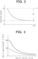
- FIG. 2 is a graph showing the time course of electrostatic capacity.
- FIG. 3 is a graph showing the attenuation status of the electrostatic capacity at the peak of point defects.
- FIG. 4 is a graph showing the relation between signal intensity due to the point defects and a temperature.
- FIG. 5 is a conceptual diagram of a semiconductor manufacturing system having the semiconductor wafer evaluation apparatus according to the embodiment of the present invention.
- FIG. 6 is a flowchart illustrating an example of control actions of a semiconductor wafer manufacturing method according to the embodiment of the present invention.
- FIG. 7 is a graph showing the in-plane distribution of a point defect density.
- FIGS. 1 to 3 A semiconductor wafer evaluation apparatus according to one embodiment of the present invention will be described based on FIGS. 1 to 3 .
- FIG. 1 shows the schematic configuration of an evaluation apparatus 21 which is the semiconductor wafer evaluation apparatus according to the one embodiment of the present invention.
- FIG. 2 shows a graph representing the time course of electrostatic capacity.
- FIG. 3 shows the attenuation curve of the electrostatic capacity at the peak of point defects (for example, Z 1/2 center defects in a SiC single crystal).
- FIG. 4 shows a graph representing a temperature sweep spectrum indicating the relation between signal intensity due to the point defects and a temperature. The Z 1/2 center is ascribed to a carbon vacancy.
- the evaluation apparatus 21 is equipped with a table 22 on which a semiconductor wafer 11 , an object to be evaluated, is placed, and which is supported so as to be reciprocatable in a plane.
- a probe means 23 as a means of contact is provided which contacts the semiconductor wafer 11 placed on the table 22 and which can reciprocate in the plane in a direction perpendicular to the table 22 .
- the probe means 23 is structured to bring mercury (Schottky electrode), which is liquefied at room temperature, as a contact maker 24 into contact with the semiconductor wafer 11 .
- the probe means 23 is rendered movable, owing to the reciprocation of the table 22 and the probe means 23 itself, to any position in the plane of the semiconductor wafer 11 .
- the evaluation apparatus 21 may be equipped with a moving means 30 .
- the moving means 30 is connected to the table 22 .
- the moving means 30 may be connected to the probe means 23 .
- the moving means is, for example, a motor.
- the moving means 30 may be a manually movable dial, screw or the like.
- the moving means 30 moves the contact maker relatively with respect to the planar direction of the semiconductor wafer.
- the probe means 23 can move the contact maker to any position in the plane of the semiconductor wafer 11 , for example, within the range of the semiconductor wafer 11 with a diameter of 150 mm or more, preferably, 300 mm or more. Thus, even in the case of the semiconductor wafer 11 having a large diameter, the in-plane distribution of point defects in the entire semiconductor wafer 11 can be grasped.
- a pulse power supply 25 as a power supply means, is provided which applies a voltage to the contact maker 24 (mercury) of the probe means 23 via a means 10 for compensating for parasitic inductance and parasitic capacity.
- the pulse power supply 25 has the function of intermittently bringing the state of voltage application (application control means).
- the evaluation apparatus 21 is equipped with a capacity meter 26 for measuring the electrostatic capacity of the semiconductor wafer 11 when the voltage is intermittently applied by the pulse power supply 25 .
- the electrostatic capacity changes over time from C2 (1) to C1 (3) through the process of (2). Based on these changes in the electrostatic capacity with the passage of time (values of the electrostatic capacity after a lapse of a predetermined time), the trap level and density of the point defects can be confirmed. Concretely, in (1) where the voltage has been applied, the density of the electrons or holes trapped corresponds to the density of the point defects. Thus, the changes in the electrostatic capacity are proportional to the density of the point defects approximately.
- the above-described evaluation apparatus 21 therefore, makes it possible to evaluate easily the density of point defects which are crystal defects of the semiconductor wafer 11 .
- the attenuation status of the electrostatic capacity of the point defect (carbon vacancy defect) peak in the silicon carbide semiconductor wafer has been confirmed. That is, the following findings have been obtained: If the point defects (carbon vacancy defects) are large (indicated by a solid line), the signal intensity for detection of the electrostatic capacity lowers with the passage of time. If the point defects (carbon vacancy defects) are small (indicated by a dashed line), with the absolute value of the signal intensity being lower than the case where the point defects are large, the signal intensity for detection of the electrostatic capacity declines over time (i.e., the attenuation of the electrostatic capacity has been confirmed).
- the status of the electrostatic capacity measured by the capacity meter 26 is sent to an evaluation means 27 .
- the evaluation means 27 the state (kinds, density, etc.) of the point defects of the semiconductor wafer 11 is evaluated based on the status of the electrostatic capacity of the semiconductor wafer 11 .
- the attenuation curve of the electrostatic capacity is approximated by an exponential function (Napier's constant is the base) to determine the amount of change in the signal intensity, and the defect density can be calculated using the value of the doping density that has been determined beforehand.
- a time constant is calculated from the exponent of the exponential function to evaluate an energetic depth in the bandgap of the defects.
- Nt is approximately calculated as 2Nx
- Nt may be multiplied by a correction term for correcting an error due to a nonionized region at the tip of the depletion layer.
- the point defect is a defect whose signal peaks at a temperature in the vicinity of room temperature. It is measured concretely by utilization of a correlation function (correlator method). This method is applicable to a defect which can be adjusted so that an electrical signal peak is obtained at around room temperature.
- a correlation function correlator method
- This method is applicable to a defect which can be adjusted so that an electrical signal peak is obtained at around room temperature.
- the correlation function described in the literature Y. Tokuda, N. Shimizu, and A. Usami, Jpn. J. Appln. Phys. 18, 309 (1979) can be utilized.
- the point defects which have been observed with their peak appearing in a state higher than room temperature (the state indicated by a dashed line), can be observed in a state near room temperature (the state indicated by a solid line), by adjusting the measurement conditions (period of the correlation function).
- An example of the point defects at around room temperature is Z 1/2 center defects in the SiC single crystal.
- the period of the correlation function which enables the maximum value of the signal intensity to be obtained is determined.
- the optimal value of the period of the correlation function depends on the kind of the defect (energetic depth of the defect). In order to evaluate a plurality of defects, therefore, an appropriate value needs to be used for each of them.
- the relative value can be used for evaluation of the uniformity of the defect density in the wafer plane.
- the defect density will be undervalued and, in a region where the defect density is low, the values may be below the lower limit of detection.
- an evaluation method involving measurements using a temperature sweep may be available in an attempt to evaluate unknown defects.
- there is no need to provide a massive cooling device or high-temperature heating device for adjusting the wafer temperature and it suffices to annex a heater for temperature control to room temperature or a temperature close to room temperature.
- the cost of equipment can be kept low.
- the pulse power supply 25 has the function of varying the applied voltage. By raising the applied voltage from the pulse power supply 25 (for example, to 100V), the state (kinds, density, etc.) of the point defects at a location deep in the depth direction of the semiconductor wafer 11 is evaluated in the evaluation means 27 . By making measurements while varying the applied voltage, the depth profile of the state of the defects can be acquired.
- the evaluation apparatus 21 can be configured to have a photoirradiation means 29 for performing irradiation with light having energy equal to or above the bandgap of the semiconductor wafer 11 .
- a photoirradiation means 29 for performing irradiation with light having energy equal to or above the bandgap of the semiconductor wafer 11 .
- the evaluation apparatus can be applied to defects forming a defect level in a bandgap near a conduction band; in a p-type semiconductor, the evaluation apparatus can be applied to defects forming a defect level in a bandgap near a valence band.
- the evaluation apparatus can be applied to defects forming a defect level in a bandgap near a valence band; in a p-type semiconductor, the evaluation apparatus can be applied to defects forming a defect level in a bandgap near a conduction band.
- the evaluation apparatus can also evaluate the status of B-related defects in an n-type SiC crystal.
- B defects are formed by B impurities unintentionally introduced during the crystal growth of SiC, and affect the doping density of the n-type SiC crystal.
- the evaluation apparatus can be applied to the quality control of the wafer.
- the evaluation apparatus can be applied to evaluating the density of point defects called a D center which is composite defects composed of B defects and carbon vacancies.
- the evaluation apparatus is also applicable to the density evaluation of defects attributed to an unintentionally introduced transition metal element, in addition to B impurities.
- the evaluation apparatus 21 of the foregoing configuration applies voltage intermittently, with the contact maker 24 (mercury) in contact with the semiconductor wafer 11 , and can evaluate the status of point defects (kinds, density, etc.: e.g., carbon vacancy density in the SiC crystal) based on the status of the electrostatic capacity of the semiconductor wafer 11 . Since the metal (mercury) liquefied at room temperature can be used as the Schottky electrode, it is unnecessary to cut out the semiconductor wafer 11 partly and stack a metal electrode for the purpose of evaluation. It becomes possible to evaluate the point defects of the entire semiconductor wafer directly.
- the contact maker 24 (mercury) is moved relatively to any position in the plane of the semiconductor wafer 11 , and voltage is applied intermittently, whereby the distribution of point defects (e.g., distribution of density, etc.) in the plane of the semiconductor wafer 11 can be evaluated.
- point defects e.g., distribution of density, etc.
- the following embodiment shows an example in which a silicon carbide semiconductor is applied as the semiconductor wafer 11 .
- the density of carbon vacancies (carbon vacancy density) can be evaluated as point defects.
- FIG. 5 shows the conceptual configuration of a semiconductor manufacturing system having the semiconductor wafer evaluation apparatus according to the one embodiment of the present invention.
- FIG. 6 is a flowchart illustrating an example of control actions by a control means 12 .
- a silicon carbide single crystal manufacturing device 1 As shown in FIG. 5 , a silicon carbide single crystal manufacturing device 1 , a semiconductor manufacturing means, epitaxially grows a silicon carbide single crystal (SiC single crystal) by chemical vapor deposition, for example.
- the silicon carbide single crystal manufacturing device 1 is a device equipped with a raw material gas supply device, a temperature control means, etc.
- a seed substrate is disposed on a susceptor, and a raw material gas is supplied to obtain a semiconductor wafer 11 having a SiC single crystal grown on the seed substrate.
- the silicon carbide single crystal manufacturing device 1 is subject to control by the control means 12 over the pressure of the manufacturing device, the composition of the raw material gas supplied from the raw material gas supply device (C/Si ratio, addition rates of additives such as N 2 , Al and B, and so on), the amount of the gas supplied, the supply position (supply angle) of the raw material gas, etc.
- the state of the susceptor (number of revolutions, position of rotation axis, etc.) is also adjusted by the control means 12 .
- the temperature control means is controlled by the control means 12 and adjusted to a predetermined high temperature state.
- the conditions for growth of the SiC single crystal are adjusted in accordance with information from the evaluation apparatus 21 , the semiconductor wafer evaluation apparatus of the present invention.
- the evaluation apparatus 21 the state of point defects (kinds, density of the point defects) of an epitaxial film of the semiconductor wafer 11 is found.
- the control means 12 the conditions for growth of the SiC single crystal (distribution of the point defects, etc.) by the silicon carbide single crystal manufacturing device 1 are adjusted and controlled in accordance with the results of evaluation by the evaluation apparatus 21 .
- the control means 12 can judge the silicon carbide single crystal manufacturing device 1 to be malfunctioning. As a result, maintenance of the silicon carbide single crystal manufacturing device 1 , for example, can be put under management. Thus, the malfunction of the device can be grasped so as not to continue manufacturing products which do not achieve the desired performance.
- the control means 12 determines, for example, carbon vacancy density, and controls the composition or the like of the raw material gas so that the carbon vacancy density determined will be in a desired state. By so doing, control can be exercised so that the carbon vacancy density is maintained in the desired state. If the carbon vacancy density fails to enter the desired state even upon control for maintaining the carbon vacancy density in the desired state, the control means 12 judges the silicon carbide single crystal manufacturing device 1 to be deficient, and can take a necessary measure.
- the control means 12 also finds point defects related to the additives (related to impurities), and controls the flow rate of the raw material gas (doping gas) so that the density of the found point defects will be in a desired state. By so doing, the state of the impurities-related point defects can be maintained in the desired state.
- the applied voltage from the pulse power supply 25 is raised to vary the measured voltage, thereby evaluating the state (kinds, density, etc.) of the point defects at a location deep in the depth direction of the semiconductor wafer 11 .
- This way of evaluation combined with the control means makes it possible to control the characteristics in the depth direction of the epiwafer.
- a multi-layered epiwafer having characteristics changed in the depth direction can be prepared, and the state in the depth direction can be confirmed by the evaluation apparatus 21 .
- Step S 1 point defects (kinds, density of point defects: point defect density A) of the epitaxial film based on changes in the electrostatic capacity are read in. It is determined in Step S 2 whether or not the read-in point defect density A is equal to or less than a target value B (threshold value). If, in Step S 2 , it is determined that the point defect density A is equal to or less than the target value B, the point defect density is taken to be in the desired state, and the program comes to an end. Thus, the manufacturing of the semiconductor wafer 11 is continued as such.
- Step S 3 it is determined in Step S 3 whether or not the point defect density A is equal to or less than a value C which is higher than the target value B. If, in Step S 3 , the point defect density A is judged to be equal to or less than the value C, the raw material gas supply device is controlled. In Step S 4 , the amount of the raw material gas, for example, is changed so that the C/Si ratio of the raw material gas is changed. Thus, the point defect density A is controlled to fall into the desired state (equal to or less than the target value B, the threshold value).
- Step S 3 If, in Step S 3 , the point defect density A is judged to exceed the value C, the temperature control means is controlled.
- Step S 5 the temperature within the treating chamber, for example, is adjusted (temperature change) so that the point defect density A is controlled to be in the desired state (equal to or less than the target value B, the threshold value).
- Step S 5 it is also possible to change the supply amount, supply angle, etc. of the gas in addition.
- Step S 6 After the supply status of the raw material gas is changed in Step S 4 , it is determined in Step S 6 whether or not the point defect density A is equal to or less than the target value B (threshold value). That is, it is determined whether or not the point defect density A has been brought into the desired state by changing the supply status of the raw material gas.
- Step S 6 If, in Step S 6 , it is determined that the point defect density A is equal to or less than the target value B, the point defect density is taken to be in the desired state, and the program ends, whereafter the manufacture of the semiconductor wafer 11 is continued as such.
- the semiconductor wafer 11 with the desired performance maintained can be manufactured by evaluating the point defect density (e.g., carbon vacancy density) of the semiconductor wafer 11 by means of the evaluation apparatus 21 and controlling the state of the point defect density by the control means 12 .
- the point defect density e.g., carbon vacancy density
- Step S 6 If it is determined in Step S 6 that the point defect density A exceeds the target value B, it is judged that the point defect density A has not decreased (the desired point defect density is not obtained) even after changing the supply status of the raw material gas. Thus, the program proceeds to Step S 7 to determine that the silicon carbide single crystal manufacturing device 1 is malfunctioning. Then, the program comes to an end.
- Step S 7 the silicon carbide single crystal manufacturing device 1 is judged to have a malfunction, the device is stopped to interrupt the manufacture of the semiconductor wafer 11 , and maintenance or the like of the silicon carbide single crystal manufacturing device 1 can be implemented.
- the maintenance of the silicon carbide single crystal manufacturing device 1 includes, for example, replacement of members constituting the silicon carbide single crystal manufacturing device 1 , positional adjustment of the members, and cleaning of the silicon carbide single crystal manufacturing device 1 .
- the malfunction of the silicon carbide single crystal manufacturing device 1 itself can be determined, and managemental action on maintenance or the like of the silicon carbide single crystal manufacturing device 1 can be carried out.
- the malfunction of the silicon carbide single crystal manufacturing device 1 can be grasped, and it can be avoided to continue manufacturing the semiconductor wafer 11 (product) which does not provide the desired performance.
- the so configured semiconductor wafer manufacturing system can maintain the quality of the semiconductor wafer 11 in the desired state, namely, the desired state of point defects (the state where the desired carrier lifetime is obtained). Moreover, the system can control the conditions of the silicon carbide single crystal manufacturing device 1 so as to manufacture the semiconductor wafer 11 in the desired state of point defects, and enables the device 1 to manufacture the semiconductor wafer 11 in a stable state. Furthermore, the system can grasp the malfunction of the silicon carbide single crystal manufacturing device 1 , and can prevent the device 1 from continuing the manufacture of the semiconductor wafer 11 (product) which does not provide the desired performance.
- FIG. 7 shows the in-plane distribution of the point defect density.
- the relative values (%) of the density of point defects in the plane of the semiconductor wafer 11 can be evaluated as an example, as shown in FIG. 7 . That is, variations in the point defects in the plane of the semiconductor wafer 11 can be evaluated. In the example shown in FIG. 7 , the relative values (%) of the density of the point defects in the plane of the semiconductor wafer 11 can be confirmed to fall within the range of ⁇ S 1 .
- the variations in the point defects in the plane of the semiconductor wafer 11 are evaluated, whereby the variations in the defect density in the plane of the semiconductor wafer 11 can be managed.
- the point defect density in the plane of the semiconductor wafer 11 is evaluated to determine the malfunction of the silicon carbide single crystal manufacturing device 1 .
- the semiconductor wafer evaluation apparatus (evaluation apparatus 21 ) of the present invention described above brings the contact maker 24 (mercury) into contact with the semiconductor wafer 11 to apply voltage intermittently, and evaluates the state (kinds, density) of point defects based on the status of the electrostatic capacity of the semiconductor wafer 11 . In this manner, the metal (mercury) liquefied at room temperature can be used as a Schottky electrode.
- the present invention can be utilized in the industrial fields of semiconductor wafer evaluation apparatuses and semiconductor wafer manufacturing methods.
Landscapes
- Chemical & Material Sciences (AREA)
- Physics & Mathematics (AREA)
- Organic Chemistry (AREA)
- Engineering & Computer Science (AREA)
- Materials Engineering (AREA)
- Metallurgy (AREA)
- General Physics & Mathematics (AREA)
- General Chemical & Material Sciences (AREA)
- Chemical Kinetics & Catalysis (AREA)
- Mechanical Engineering (AREA)
- Inorganic Chemistry (AREA)
- Crystallography & Structural Chemistry (AREA)
- Health & Medical Sciences (AREA)
- Electromagnetism (AREA)
- Toxicology (AREA)
- Testing Or Measuring Of Semiconductors Or The Like (AREA)
- Crystals, And After-Treatments Of Crystals (AREA)
Abstract
Description
-
- 1 Silicon carbide single crystal manufacturing device
- 10 Means for compensating for parasitic inductance and parasitic capacity
- 11 Semiconductor wafer
- 12 Control means
- 21 Evaluation apparatus
- 22 Table
- 23 Probe means
- 24 Contact maker
- 25 Pulse power supply
- 26 Capacity meter
- 27 Evaluation means
- 29 Photoirradiation means
- 30 Moving means
Claims (15)
Applications Claiming Priority (2)
| Application Number | Priority Date | Filing Date | Title |
|---|---|---|---|
| JP2020185713A JP7588495B2 (en) | 2020-11-06 | 2020-11-06 | Semiconductor wafer evaluation device and semiconductor wafer manufacturing method |
| JP2020-185713 | 2020-11-06 |
Publications (2)
| Publication Number | Publication Date |
|---|---|
| US20220146564A1 US20220146564A1 (en) | 2022-05-12 |
| US11906569B2 true US11906569B2 (en) | 2024-02-20 |
Family
ID=81454302
Family Applications (1)
| Application Number | Title | Priority Date | Filing Date |
|---|---|---|---|
| US17/519,679 Active 2042-04-10 US11906569B2 (en) | 2020-11-06 | 2021-11-05 | Semiconductor wafer evaluation apparatus and semiconductor wafer manufacturing method |
Country Status (2)
| Country | Link |
|---|---|
| US (1) | US11906569B2 (en) |
| JP (1) | JP7588495B2 (en) |
Families Citing this family (1)
| Publication number | Priority date | Publication date | Assignee | Title |
|---|---|---|---|---|
| EP4717802A1 (en) * | 2024-09-30 | 2026-04-01 | Resonac Corporation | Sic epitaxial wafer, method for manufacturing sic epitaxial wafer, and sic device |
Citations (5)
| Publication number | Priority date | Publication date | Assignee | Title |
|---|---|---|---|---|
| US3794912A (en) * | 1971-05-19 | 1974-02-26 | Philips Corp | Contact device using conductive fluid for measuring resistance and capacitance of semiconductor |
| JP2007318031A (en) * | 2006-05-29 | 2007-12-06 | Central Res Inst Of Electric Power Ind | Method for manufacturing silicon carbide semiconductor element |
| US20160086799A1 (en) * | 2014-09-22 | 2016-03-24 | Sumitomo Electric Industries, Ltd. | Method of Producing Silicon Carbide Epitaxial Substrate, Silicon Carbide Epitaxial Substrate, and Silicon Carbide Semiconductor Device |
| JP2016100591A (en) | 2014-11-26 | 2016-05-30 | 株式会社東芝 | Semiconductor device manufacturing method and semiconductor device |
| US20170160335A1 (en) * | 2014-06-25 | 2017-06-08 | Shin-Etsu Handotai Co., Ltd. | Method for evaluating defect region of semiconductor substrate |
Family Cites Families (3)
| Publication number | Priority date | Publication date | Assignee | Title |
|---|---|---|---|---|
| JPS5415751B1 (en) * | 1967-08-30 | 1979-06-16 | ||
| JP4946264B2 (en) * | 2006-08-23 | 2012-06-06 | 日立金属株式会社 | Method for manufacturing silicon carbide semiconductor epitaxial substrate |
| JP6023497B2 (en) * | 2012-07-30 | 2016-11-09 | 学校法人中部大学 | Wide gap semiconductor band gap electronic property measuring method and wide gap semiconductor band gap electronic property measuring apparatus |
-
2020
- 2020-11-06 JP JP2020185713A patent/JP7588495B2/en active Active
-
2021
- 2021-11-05 US US17/519,679 patent/US11906569B2/en active Active
Patent Citations (5)
| Publication number | Priority date | Publication date | Assignee | Title |
|---|---|---|---|---|
| US3794912A (en) * | 1971-05-19 | 1974-02-26 | Philips Corp | Contact device using conductive fluid for measuring resistance and capacitance of semiconductor |
| JP2007318031A (en) * | 2006-05-29 | 2007-12-06 | Central Res Inst Of Electric Power Ind | Method for manufacturing silicon carbide semiconductor element |
| US20170160335A1 (en) * | 2014-06-25 | 2017-06-08 | Shin-Etsu Handotai Co., Ltd. | Method for evaluating defect region of semiconductor substrate |
| US20160086799A1 (en) * | 2014-09-22 | 2016-03-24 | Sumitomo Electric Industries, Ltd. | Method of Producing Silicon Carbide Epitaxial Substrate, Silicon Carbide Epitaxial Substrate, and Silicon Carbide Semiconductor Device |
| JP2016100591A (en) | 2014-11-26 | 2016-05-30 | 株式会社東芝 | Semiconductor device manufacturing method and semiconductor device |
Non-Patent Citations (1)
| Title |
|---|
| Espacenet English translation of JP2007318031A Manufacturing Method of Silicon Carbide Semiconductor Element (Year: 2007). * |
Also Published As
| Publication number | Publication date |
|---|---|
| JP7588495B2 (en) | 2024-11-22 |
| JP2022075127A (en) | 2022-05-18 |
| US20220146564A1 (en) | 2022-05-12 |
Similar Documents
| Publication | Publication Date | Title |
|---|---|---|
| US10615085B2 (en) | Method for predicting thickness of oxide layer of silicon wafer | |
| CN101443488A (en) | Method for producing III-N bulk crystals and free-standing III-N substrates, and III-N bulk crystals and free-standing III-N substrates | |
| US11906569B2 (en) | Semiconductor wafer evaluation apparatus and semiconductor wafer manufacturing method | |
| US20220173001A1 (en) | SiC EPITAXIAL WAFER AND METHOD FOR PRODUCING SiC EPITAXIAL WAFER | |
| KR102595667B1 (en) | SiC SUBSTRATE AND SiC INGOT | |
| CN118854445A (en) | A method for controlling silicon carbide epitaxial growth temperature | |
| CN117711935A (en) | Method and device for reducing warping degree of epitaxial wafer | |
| JP2002531935A (en) | Method and system for manufacturing semiconductor crystals with temperature control | |
| CN113035697B (en) | A method for optimizing process parameters for epitaxial growth of high electron mobility devices | |
| CN113252195B (en) | A method for determining substrate temperature in molecular beam epitaxy equipment | |
| CN119308013A (en) | A method for monitoring and calibrating epitaxial cavity temperature | |
| US11183433B2 (en) | Method of evaluating silicon layer and a method of manufacturing silicon epitaxial wafer | |
| CN113314951B (en) | VCSEL chip oxidation real-time monitoring method and device | |
| EP4717802A1 (en) | Sic epitaxial wafer, method for manufacturing sic epitaxial wafer, and sic device | |
| CN113257706A (en) | Epitaxial wafer and doping concentration monitoring method thereof | |
| CN121046945A (en) | Debugging method of multi-sheet furnace | |
| CN119764220B (en) | A method for reducing the number of defects in silicon carbide epitaxial materials | |
| KR20100010795A (en) | Manufacturing method of resistivity standard sample of epitaxial wafer and revision method of resistivity measuring device used the resistivity standard sample manufactured by the method | |
| JP5928146B2 (en) | Semiconductor product manufacturing method and semiconductor manufacturing apparatus | |
| US7474114B2 (en) | System and method for characterizing silicon wafers | |
| WO2002000971A1 (en) | Silicon epitaxial wafer manufacturing method and silicon epitaxial wafer | |
| CN121712314A (en) | Methods to improve film thickness and slip lines after epitaxy | |
| CN109632855B (en) | Method for detecting impurity defect concentration substituting for cation position in compound semiconductor | |
| EP1933372A1 (en) | Process for producing epitaxial wafer and epitaxial wafer produced therefrom | |
| JP2025072804A (en) | SiC epitaxial wafer |
Legal Events
| Date | Code | Title | Description |
|---|---|---|---|
| AS | Assignment |
Owner name: SHOWA DENKO K.K., JAPAN Free format text: ASSIGNMENT OF ASSIGNORS INTEREST;ASSIGNORS:MURATA, KOICHI;KAMATA, ISAHO;TSUCHIDA, HIDEKAZU;AND OTHERS;SIGNING DATES FROM 20211019 TO 20211029;REEL/FRAME:058029/0037 |
|
| FEPP | Fee payment procedure |
Free format text: ENTITY STATUS SET TO UNDISCOUNTED (ORIGINAL EVENT CODE: BIG.); ENTITY STATUS OF PATENT OWNER: LARGE ENTITY |
|
| STPP | Information on status: patent application and granting procedure in general |
Free format text: DOCKETED NEW CASE - READY FOR EXAMINATION |
|
| STPP | Information on status: patent application and granting procedure in general |
Free format text: NON FINAL ACTION MAILED |
|
| STPP | Information on status: patent application and granting procedure in general |
Free format text: RESPONSE TO NON-FINAL OFFICE ACTION ENTERED AND FORWARDED TO EXAMINER |
|
| AS | Assignment |
Owner name: RESONAC CORPORATION, JAPAN Free format text: CHANGE OF NAME;ASSIGNOR:SHOWA DENKO K.K.;REEL/FRAME:064082/0513 Effective date: 20230623 |
|
| STPP | Information on status: patent application and granting procedure in general |
Free format text: NON FINAL ACTION MAILED |
|
| STPP | Information on status: patent application and granting procedure in general |
Free format text: RESPONSE TO NON-FINAL OFFICE ACTION ENTERED AND FORWARDED TO EXAMINER |
|
| STPP | Information on status: patent application and granting procedure in general |
Free format text: NOTICE OF ALLOWANCE MAILED -- APPLICATION RECEIVED IN OFFICE OF PUBLICATIONS |
|
| STPP | Information on status: patent application and granting procedure in general |
Free format text: PUBLICATIONS -- ISSUE FEE PAYMENT RECEIVED |
|
| STPP | Information on status: patent application and granting procedure in general |
Free format text: PUBLICATIONS -- ISSUE FEE PAYMENT VERIFIED |
|
| STCF | Information on status: patent grant |
Free format text: PATENTED CASE |
|
| AS | Assignment |
Owner name: RESONAC CORPORATION, JAPAN Free format text: CHANGE OF ADDRESS;ASSIGNOR:RESONAC CORPORATION;REEL/FRAME:066547/0677 Effective date: 20231001 |