US11875843B2 - Systems and methods for improved data access speed - Google Patents
Systems and methods for improved data access speed Download PDFInfo
- Publication number
- US11875843B2 US11875843B2 US17/141,279 US202117141279A US11875843B2 US 11875843 B2 US11875843 B2 US 11875843B2 US 202117141279 A US202117141279 A US 202117141279A US 11875843 B2 US11875843 B2 US 11875843B2
- Authority
- US
- United States
- Prior art keywords
- signal
- enable signal
- input
- column selection
- memory array
- Prior art date
- Legal status (The legal status is an assumption and is not a legal conclusion. Google has not performed a legal analysis and makes no representation as to the accuracy of the status listed.)
- Active
Links
- 238000000034 method Methods 0.000 title claims abstract description 23
- 230000004044 response Effects 0.000 claims abstract description 7
- 238000010586 diagram Methods 0.000 description 20
- 230000008569 process Effects 0.000 description 6
- 230000004913 activation Effects 0.000 description 5
- 230000007704 transition Effects 0.000 description 5
- 230000003321 amplification Effects 0.000 description 4
- 238000003199 nucleic acid amplification method Methods 0.000 description 4
- 230000005540 biological transmission Effects 0.000 description 3
- 101100004199 Brassica napus BBM2 gene Proteins 0.000 description 2
- 230000003213 activating effect Effects 0.000 description 2
- 238000003491 array Methods 0.000 description 2
- 230000004075 alteration Effects 0.000 description 1
- 230000008859 change Effects 0.000 description 1
- 230000000295 complement effect Effects 0.000 description 1
- 238000004883 computer application Methods 0.000 description 1
- 238000010276 construction Methods 0.000 description 1
- 238000013500 data storage Methods 0.000 description 1
- 230000000630 rising effect Effects 0.000 description 1
- 238000006467 substitution reaction Methods 0.000 description 1
- 230000001960 triggered effect Effects 0.000 description 1
Images


Classifications
-
- G—PHYSICS
- G11—INFORMATION STORAGE
- G11C—STATIC STORES
- G11C8/00—Arrangements for selecting an address in a digital store
- G11C8/06—Address interface arrangements, e.g. address buffers
-
- G—PHYSICS
- G11—INFORMATION STORAGE
- G11C—STATIC STORES
- G11C11/00—Digital stores characterised by the use of particular electric or magnetic storage elements; Storage elements therefor
- G11C11/21—Digital stores characterised by the use of particular electric or magnetic storage elements; Storage elements therefor using electric elements
- G11C11/34—Digital stores characterised by the use of particular electric or magnetic storage elements; Storage elements therefor using electric elements using semiconductor devices
- G11C11/40—Digital stores characterised by the use of particular electric or magnetic storage elements; Storage elements therefor using electric elements using semiconductor devices using transistors
- G11C11/41—Digital stores characterised by the use of particular electric or magnetic storage elements; Storage elements therefor using electric elements using semiconductor devices using transistors forming static cells with positive feedback, i.e. cells not needing refreshing or charge regeneration, e.g. bistable multivibrator or Schmitt trigger
- G11C11/413—Auxiliary circuits, e.g. for addressing, decoding, driving, writing, sensing, timing or power reduction
- G11C11/417—Auxiliary circuits, e.g. for addressing, decoding, driving, writing, sensing, timing or power reduction for memory cells of the field-effect type
- G11C11/419—Read-write [R-W] circuits
-
- G—PHYSICS
- G11—INFORMATION STORAGE
- G11C—STATIC STORES
- G11C11/00—Digital stores characterised by the use of particular electric or magnetic storage elements; Storage elements therefor
- G11C11/21—Digital stores characterised by the use of particular electric or magnetic storage elements; Storage elements therefor using electric elements
- G11C11/34—Digital stores characterised by the use of particular electric or magnetic storage elements; Storage elements therefor using electric elements using semiconductor devices
- G11C11/40—Digital stores characterised by the use of particular electric or magnetic storage elements; Storage elements therefor using electric elements using semiconductor devices using transistors
- G11C11/41—Digital stores characterised by the use of particular electric or magnetic storage elements; Storage elements therefor using electric elements using semiconductor devices using transistors forming static cells with positive feedback, i.e. cells not needing refreshing or charge regeneration, e.g. bistable multivibrator or Schmitt trigger
- G11C11/413—Auxiliary circuits, e.g. for addressing, decoding, driving, writing, sensing, timing or power reduction
- G11C11/417—Auxiliary circuits, e.g. for addressing, decoding, driving, writing, sensing, timing or power reduction for memory cells of the field-effect type
- G11C11/418—Address circuits
-
- G—PHYSICS
- G11—INFORMATION STORAGE
- G11C—STATIC STORES
- G11C7/00—Arrangements for writing information into, or reading information out from, a digital store
- G11C7/06—Sense amplifiers; Associated circuits, e.g. timing or triggering circuits
-
- G—PHYSICS
- G11—INFORMATION STORAGE
- G11C—STATIC STORES
- G11C7/00—Arrangements for writing information into, or reading information out from, a digital store
- G11C7/06—Sense amplifiers; Associated circuits, e.g. timing or triggering circuits
- G11C7/065—Differential amplifiers of latching type
-
- G—PHYSICS
- G11—INFORMATION STORAGE
- G11C—STATIC STORES
- G11C8/00—Arrangements for selecting an address in a digital store
- G11C8/08—Word line control circuits, e.g. drivers, boosters, pull-up circuits, pull-down circuits, precharging circuits, for word lines
-
- G—PHYSICS
- G11—INFORMATION STORAGE
- G11C—STATIC STORES
- G11C7/00—Arrangements for writing information into, or reading information out from, a digital store
- G11C7/06—Sense amplifiers; Associated circuits, e.g. timing or triggering circuits
- G11C7/08—Control thereof
Definitions
- This disclosure is related to data access and particularly signal timing for coordination of access to stored data values.
- Data rates may be improved in different manners including improved data access and data transmission.
- data access process there are a variety of portions of the data access process where latency occurs and improvements may be realized.
- FIG. 1 is a block diagram depicting a memory device in accordance with an embodiment.
- FIG. 2 is a block diagram depicting example details of column selection in accordance with embodiments.
- FIG. 3 is a diagram depicting generation of first and second enable signals by an enable signal generating circuit in accordance with embodiments.
- FIG. 4 is a diagram depicting column selection circuitry for generating column selection signals in accordance with embodiments.
- FIG. 5 is a diagram depicting operation of a sense amplifier in accordance with an embodiment.
- FIG. 6 is a signal diagram depicting operation of a memory device in accordance with an embodiment.
- FIG. 7 is a block diagram depicting an enable signal generating circuit operating on a multibank memory device in accordance with an embodiment.
- FIG. 8 is a diagram depicting column multiplexer circuitry for selecting a column from one of multiple memory banks in accordance with an embodiment.
- FIG. 9 is a diagram depicting a multi-bank memory device circuit in accordance with an embodiment.
- FIG. 10 is a flow diagram depicting a method of operating a memory device in accordance with an embodiment.
- Computing system performance can often be improved by lessening the time it takes to access data from a data storage device, such as an SRAM memory (e.g., an SRAM register file). Accessing data from a memory may occur in a series of stages. In one example, a clock transition initiates the data access process. An address of the data to be accessed is decoded, and a word line signal is provided to a word line of a memory array based on the address. Data (e.g., a differential data signal on a bit line (BTS) and a bit complement line (BBS)) from one or more columns of the selected word of memory is accessed and provided to a sense amplifier. The sense amplifier senses a difference between signal levels of the received signals and drives one output line (e.g., QT, QB) low and one output line high based on the sensed difference.
- a data storage device such as an SRAM memory (e.g., an SRAM register file). Accessing data from a memory may occur in a series of stages. In
- Each stage of the data access process is typically associated with some latency. For example, there is a latency associated with decoding a received address that indicates data to be access from the memory array to identify which word line signal to activate. There is also a latency associated with transferring data from an associated data location (i.e., a word/column identified in an address) to the sense amplifier.
- Systems and methods as described herein can, in embodiments, coordinate selection of data from a column of a selected memory array word and activation of a sense amplifier such that word line-to-sense amplifier latency is minimized.
- FIG. 1 is a block diagram depicting a memory device in accordance with an embodiment.
- the memory device 100 includes a memory array 102 which may be divided into a plurality of rows and columns, where each row/column location includes a memory cell (e.g., a 6T SRAM cell).
- a column selection circuit 104 is coupled to the memory array and is configured to generate one or more column selection signals 106 .
- a sense amplifier 108 is configured to receive data signals (e.g., on differential signal lines BTS/BBS) from the memory array 102 .
- An enable signal generating circuit 110 coordinates column selection at 104 and sense amplification at 108 by generating a first enable signal and a second enable signal.
- column selection circuit 104 generates the column selection signal 106 based on the first enable signal, and the sense amplifier 108 receives a data signal from the memory array 102 in response to the second enable signal. In an alternative example embodiment, the sense amplifier 108 further receives the data signal from the memory array 102 based on the first enable signal.
- FIG. 2 is a block diagram depicting example details of column selection in accordance with embodiments.
- FIG. 2 depicts a memory device 200 that includes a memory array 102 .
- the memory array 102 may include memory cell circuitry 204 that includes rows and columns of memory cells 203 (connected to word line signals WLTop . . . WL0) as well as precharge circuits 205 (connected to control signal BLPCHB) for enabling memory cells 203 to promptly output signals representative of data stored within the data cells.
- the memory device 200 is configured to receive an address of an identified memory cell from which data is to be accessed. The address is decoded and a word line (e.g., WLTop, . . .
- WL0 WL0 associated with a row where the identified cell resides is asserted (e.g., based on most significant bits of the address). That asserted word line may activate each of the cells in that row such that each cell in the selected row provides respective data signals on BTn, BBn (e.g., a first cell in the selected row provides differential data signals on BT0, BB0, a third cell in the selected row provides differential data signals on BT2, BB2).
- a column selection circuit 104 i.e., column multiplexer (MUX) then selects a column of the memory array (e.g., based on the least significant bits of the address) and forwards data signals from the selected memory cell(s) to a sense amplifier 108 on differential signal lines BTS/BBS.
- a sense amplifier 108 For example, an active low column selection signal on SAEB_CME[0] activates transistors BTM0, BBM0 such that signals received at BT0, BB0 are passed to BTS, BBS as outputs from the memory array 102 , respectively.
- a low column selection signal on SAEB_CME[2] activates transistors BTM2, BBM2 such that signals received at BT2, BB2 are passed to BTS, BBS as outputs from the memory array 102 , respectively.
- the sense amplifier 108 senses a difference in signal levels of received signals BTS/BBS and outputs a corresponding differential output signal at QT/QB.
- the example of FIG. 2 includes an enable signal generating circuit 110 .
- the enable signal generating circuit 110 coordinates column selection by the column selection circuit 104 and activation of the sense amplifier 108 by providing the column selection circuit 104 a first enable signal (SAEB) as described further herein.
- the enable signal generating circuit 110 further provides a second enable signal (SAE_INT) to the sense amplifier 108 , where in embodiments the second enable signal is based on the first enable signal (e.g., the second enable signal is activated a predetermined period of time after the first enable signal is activated as described in further detail herein with respect to FIG. 3 , where SAE_INT is activated one inverter transition period after activation of SAEB).
- the enable signal generating circuit also provides the first enable signal (SAEB) to the sense amplifier 108 .
- SAEB first enable signal
- Coordination of column selection and operation of the sense amplifier can, in embodiments, streamline transmission of data from the memory cells to the sense amplifier, such as by using a reduced number of gating structures (e.g., transistors) on the path between the memory cells and the sense amplifier outputs.
- use of the first and second enable signals from the column selection circuit 104 enables direct connection from memory array 102 (see, e.g., BTS, BBS outputs from memory array 102 as depicted in FIG. 2 ) to input nodes of the sense amplifier 108 (see, e.g., BTS, BTS inputs to as depicted in FIG. 5 ) without the use of any intervening transistors or logic gates.
- FIG. 3 is a diagram depicting generation of first and second enable signals by an enable signal generating circuit in accordance with embodiments.
- the enable signal generating circuit receives an input enable signal (SAE), which in embodiments modified to incorporate an enable signal generating circuit and/or other features described herein may be analogous to a sense amplifier enable signal.
- SAE input enable signal
- the enable signal generating circuit generates the first enable signal (SAEB) by inverting the input enable signal (SAE) providing an inverted output a predetermined period of time after the input enable signal is received.
- the enable signal generating circuit further generates the second enable signal (SAE_INT) by inverting the first enable signal (SAEB) providing an inverted output a predetermined period of time after transition of the first enable signal (SAEB).
- FIG. 4 is a diagram depicting column selection circuitry for generating column selection signals 106 in accordance with embodiments.
- a column selection circuit 104 that is configured to provide an active low column selection signal to one of four columns of a memory array 102 includes four not-and (NAND) gates in an embodiment.
- the column selection circuit routes the first enable signal (SAEB) from the enable signal generating circuit 110 to each of the NAND gates along with one of four column indication signals CME[0] . . . CME[3], one of which is activated at 402 based on decoding of the two least significant bits of an address of data being accessed.
- SAEB first enable signal
- an active low column selection signal is output to the memory array column associated with the indicated column.
- SAEB first enable signal
- column indicator CME[0] when the first enable signal SAEB and column indicator CME[0] are high, SAEB_CME[0] (routed to transistors BTM0, BBM0 in the example of FIG. 2 ) is output active low enabling passage of a data indicating signal from the first column of the memory array 102 to pass to output lines BTS/BBS.
- SAEB_CME[2] routed to transistors BTM2, BBM2 in the example of FIG. 2
- SAEB_CME[2] when the first enable signal SAEB and column indicator CME[2] are high, SAEB_CME[2] (routed to transistors BTM2, BBM2 in the example of FIG. 2 ) is output active low, enabling passage of a data indicating signal from the fourth column of the memory array 102 to pass to output lines BTS/BBS.
- FIG. 5 is a diagram depicting operation of a sense amplifier 108 in accordance with an embodiment.
- a sense amplifier precharge circuit 502 precharges input nodes BTS/BBS to a high level based on an active low enable circuit SEP, which in embodiments is activated at or about the time that a word line is activated at the memory array 102 .
- a sense amplification portion 504 includes the first input node BTS and the second input node BBS, which receive signals from the memory array.
- a first inverter 506 is responsive to the first input node BTS and provides a first output QB from the sense amplifier 108 .
- a second inverter 508 is responsive to the second input node BTB and provides a second output QT from the sense amplifier 108 .
- the sense-amplifying portion 504 further includes circuitry configured to push one of the first and second input nodes (BTS/BBS) high and the other low based on a detected voltage difference between the first and second input nodes.
- the sense amplifying portion 504 includes two P-type transistors (MPXT, MPXB), each connected to a voltage source and an intermediate node) and two N-type transistors (MNXT, MNXB), each connected to a respective one of the intermediate nodes and a sense amplifier transistor (MNSAE), which is further connected to a ground node.
- the gates of one of the P-type and one of the N-type transistors are connected to the first input node BTS; and the gates of one of the P-type and one of the N-type transistors (MPXT, MNXT) are connected to the second input node BBS.
- the sense amplifying portion 504 in one embodiment is primed for operation by a high first enable signal (SAEB) at 510 , followed by a high second enable signal (SAE_INT), which activates the sense amplifier transistor (MNSAE).
- SAEB high first enable signal
- SAE_INT high second enable signal
- node 510 is not connected to the first enable signal.
- input nodes BTS, BBS are initially pre-charged to high levels by precharge circuit 502 .
- Data signals are received at the input nodes BTS/BBS from the memory array after activation of the first enable signal (e.g., via a column selection signal from the column selection circuit).
- the data signals received at BTS/BBS pull one of the input nodes lower than the other.
- the sense amplifying portion 504 drives whichever input node BTS/BBS is currently at a lower level to the ground level while at the same time driving the other input node to a high level.
- Inverters 506 , 508 invert the resulting signals at the input nodes BTS/BBS, producing corresponding outputs at QT, QB.
- FIG. 6 is a signal diagram depicting operation of a memory device in accordance with an embodiment.
- a data cell in the top row, fourth column is selected.
- a data access process is initiated at 602 by a rising clock signal, which initiates decoding of the most significant bits of a provided address that dictate which of a plurality of word lines is to be activated.
- the word line (WLTOP) identified by the most significant bits of the address and a bit line precharge circuit control signal are activated.
- WLTOP word line
- each of the bit cells in the top row drive their respective BTn/BBn signal lines to levels corresponding to the data value stored therein.
- Top Row, Column 4 is selected by the address, signals on BB[2:0], BT[2:0] are Don't Care values and are not indicated in FIG. 6 .
- the data value in Top Row, Column 4 pulls BT3 toward a low value while keeping BB3 near a high level, beginning at 606 .
- an input enable signal (SAE) provided to the enable signal generating circuit transitions high.
- the enable signal generating circuit generates the first enable signal (SAEB) at 610 which is received by the column selection circuit and used to generate column selection signal SAEB_CME[3] at 612 based on the first enable signal and a column indicating signal CME[3] generated based on decoding of the least significant bits of the address.
- the SAEB_CME[3] signal generated by the column selection circuit selects the fourth column of the top word line of the memory array and initiates transmission of the signal from BT3/BB3 to the sense amplifier via BTS/BBS, respectively.
- BTS and BBS beginning to transition based on the column selection signal (SAEB_CME[3]) at 612 .
- the first enable signal may, in embodiments, also provided to the sense amplifier to prime the sense amplifier for operation.
- the sense amplifier receives the second enable signal (SAE_INT) at 614 , which triggers sense amplifier operation.
- SAE_INT the second enable signal
- the sense amplifier senses the difference between BTS and BBS at its input nodes and drives the corresponding one of QT and QB low accordingly at 614 .
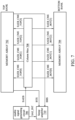
- FIG. 7 is a block diagram depicting an enable signal generating circuit operating on a multibank memory device in accordance with an embodiment.
- the memory device of FIG. 7 includes a memory array that is divided into multiple (2) memory banks, a top memory bank 702 and a bottom memory bank 704 .
- Each memory bank 702 , 704 includes multiple rows of memory cells, each row containing four columns [columns 0 . . . 3].
- An enable signal generating circuit 706 is configured to generate a first enable signal (SAEB) that is provided to a column multiplexer 708 and a second enable signal (SAE_INT) that is provided to a sense amplifier 710 .
- the first enable signal (SAEB) is used by the column multiplexer 708 to select one column from either the top bank 702 or the bottom bank 704 (e.g., based on the two least significant bits of an address and a top/bottom bank indication signal).
- FIG. 8 is a diagram depicting column multiplexer circuitry 708 for selecting a column from one of multiple memory banks 702 , 704 in accordance with an embodiment.
- the column multiplexer 708 receives the two least significant bits of an address (ADR[1:0]) which is decoded at 802 to identify which column should be selected from either the top bank 702 or bottom bank 704 by activating one of CME[0] . . . CME[3] (e.g., similar as performed above with respect to FIG. 4 ).
- the column multiplexer 708 further receives a Top/Bottom signal (e.g., on one or separate signal lines).
- ADR[1:0] the two least significant bits of an address
- CME[0] . . . CME[3] e.g., similar as performed above with respect to FIG. 4 .
- the column multiplexer 708 further receives a Top/Bottom signal (e.g., on one or separate signal lines).
- each of the NAND gates being associated with one of the columns of the two-bank memory (i.e., columns 0 . . . 3 of the top memory bank and columns 0 . . . 3 of the bottom memory bank).
- the NAND gate Upon receipt of a signal from the column decoder 802 and the top/bottom indication signal that indicates that the NAND gate is associated with the requested column/memory bank, and upon receipt of the first enable signal (SAEB), the NAND gate is configured to assert a corresponding column selection signal SAEB_CME_TOP (or BOT) [0 . . . 3].
- SAEB_CME_TOP or BOT
- the selected column of the selected memory bank provides a data-indicating signal on output lines BTS, BBS.
- the enable signal generating circuit 706 is further configured to provide the second enable signal (SAE_INT) to the sense amplifier 710 .
- the sense amplification operation is initiated on receipt of the second enable signal (SAE_INT), whereby data signals are output from the memory circuit based on that sense amplification.
- FIG. 9 is a diagram depicting a multi-bank memory device circuit in accordance with an embodiment.
- FIG. 9 depicts a memory device 900 that includes a top array 702 .
- the top memory array 702 may include memory cell circuitry 904 that includes rows and columns of memory cells 903 as well as precharge circuits 905 for enabling memory cells 903 to promptly output signals representative of data stored within the data cells.
- a bottom memory array 704 is similarly structured.
- the memory device 900 is configured to receive an address of an identified memory cell/memory bank from which data is to be accessed.
- the address is decoded and a word line associated with a row where the identified cell resides is asserted (e.g., based on most significant bits of the address).
- a word line in both the top and bottom memory arrays 702 , 704 may be activated.
- only one word line across the two memory arrays 702 , 704 may be asserted. That asserted word line may activate each of the cells in that row such that each cell in the selected row provides respective data signals on BTn, BBn.
- a column selection circuit e.g., column MUX 708 of FIG.
- FIG. 10 is a flow diagram depicting a method of operating a memory device in accordance with an embodiment. While the steps of the method may be performed using a wide variety of structures, references to some example structures are provided here for clarity.
- the method uses an enable signal circuit 110 to generate a first enable signal and a second enable signal at 1002 .
- first enable signal is provided to a column selection circuit 104
- the second enable signal is provided to a sense amplifier circuit 108 .
- the column selection circuit 104 is used at 1006 to generate a column selection signal 106 to a memory device 102 based upon the first enable signal.
- a data signal is received from the memory array 102 at the sense amplifier 108 in response to the second enable signal.
- use of the subject matter can provide high speed clock access to data stored in a memory, such as an SRAM register file.
- a memory such as an SRAM register file.
- data signals can be transmitted from a memory array to a sense amplifier directly, or substantially directly, with limited circuitry (e.g., transistors or logic gates) therebetween.
- a memory device includes a memory array, a column selection circuit coupled to the memory array, where the column selection circuit is configured to generate a column selection signal, and a sense amplifier configured to receive data signals from the memory array.
- An enable signal generating circuit is configured to generate a first enable signal and a second enable signal.
- the column selection circuit generates the column selection signal based on the first enable signal, and the sense amplifier is configured to receive a data signal from the memory array in response to the second enable signal.
- a method of operating a memory device uses an enable signal circuit to generate a first enable signal and a second enable signal.
- the first enable signal is provided to a column selection circuit, and the second enable signal to a sense amplifier circuit.
- the column selection circuit is used to generate a column selection signal to a memory device based upon the first enable signal.
- a data signal is received from the memory array at the sense amplifier in response to the second enable signal.
- an enable signal generator includes an input configured to receive an input enable signal. Logic is present for generating a first enable signal based on the input enable signal, said first enable signal being routed to a memory array column selection circuit. And further logic is present for generating a second enable signal based on the input enable signal, said second enable signal being routed to a sense amplifier.
Landscapes
- Engineering & Computer Science (AREA)
- Microelectronics & Electronic Packaging (AREA)
- Computer Hardware Design (AREA)
- Static Random-Access Memory (AREA)
- Dram (AREA)
Abstract
Description
Claims (20)
Priority Applications (4)
| Application Number | Priority Date | Filing Date | Title |
|---|---|---|---|
| US17/141,279 US11875843B2 (en) | 2020-08-31 | 2021-01-05 | Systems and methods for improved data access speed |
| CN202110903593.2A CN113808635B (en) | 2020-08-31 | 2021-08-06 | Enable signal generator, memory device and operating method thereof |
| TW110130646A TWI827968B (en) | 2020-08-31 | 2021-08-19 | Memory device and operating method thereof and enable signal generator |
| US18/503,290 US20240071481A1 (en) | 2020-08-31 | 2023-11-07 | Systems and Methods for Improved Data Access Speed |
Applications Claiming Priority (2)
| Application Number | Priority Date | Filing Date | Title |
|---|---|---|---|
| US202063072312P | 2020-08-31 | 2020-08-31 | |
| US17/141,279 US11875843B2 (en) | 2020-08-31 | 2021-01-05 | Systems and methods for improved data access speed |
Related Child Applications (1)
| Application Number | Title | Priority Date | Filing Date |
|---|---|---|---|
| US18/503,290 Continuation US20240071481A1 (en) | 2020-08-31 | 2023-11-07 | Systems and Methods for Improved Data Access Speed |
Publications (2)
| Publication Number | Publication Date |
|---|---|
| US20220068374A1 US20220068374A1 (en) | 2022-03-03 |
| US11875843B2 true US11875843B2 (en) | 2024-01-16 |
Family
ID=78893420
Family Applications (2)
| Application Number | Title | Priority Date | Filing Date |
|---|---|---|---|
| US17/141,279 Active US11875843B2 (en) | 2020-08-31 | 2021-01-05 | Systems and methods for improved data access speed |
| US18/503,290 Pending US20240071481A1 (en) | 2020-08-31 | 2023-11-07 | Systems and Methods for Improved Data Access Speed |
Family Applications After (1)
| Application Number | Title | Priority Date | Filing Date |
|---|---|---|---|
| US18/503,290 Pending US20240071481A1 (en) | 2020-08-31 | 2023-11-07 | Systems and Methods for Improved Data Access Speed |
Country Status (3)
| Country | Link |
|---|---|
| US (2) | US11875843B2 (en) |
| CN (1) | CN113808635B (en) |
| TW (1) | TWI827968B (en) |
Citations (14)
| Publication number | Priority date | Publication date | Assignee | Title |
|---|---|---|---|---|
| US6344760B1 (en) | 1999-07-28 | 2002-02-05 | Hyundai Electronics Industries Co., Ltd. | Sense amplifier drive circuit |
| US20020081789A1 (en) | 2000-11-21 | 2002-06-27 | Kim Sun Min | Sense amplifier circuit for semiconductor device |
| US20020181301A1 (en) * | 1999-12-03 | 2002-12-05 | Hiroyuki Takahashi | Semiconductor storage and method for testing the same |
| US20070183234A1 (en) * | 2006-01-27 | 2007-08-09 | Samsung Electronics Co., Ltd. | Semiconductor memory device having reduced voltage coupling between bit lines |
| US20080247249A1 (en) | 2007-04-03 | 2008-10-09 | Cheng Hung Lee | Circuit and method for a sense amplifier |
| US20090240900A1 (en) * | 2008-03-21 | 2009-09-24 | Fujitsu Limited | Memory apparatus and memory control method |
| US20110085391A1 (en) * | 2009-10-08 | 2011-04-14 | Arm Limited | Memory with improved read stability |
| US20110317478A1 (en) * | 2010-06-25 | 2011-12-29 | International Business Machines Corporation | Method and Circuit Arrangement for Performing a Write Through Operation, and SRAM Array With Write Through Capability |
| US20120127782A1 (en) | 2010-11-22 | 2012-05-24 | Fujitsu Semiconductor Limited | Static ram |
| US8289795B1 (en) | 2011-10-10 | 2012-10-16 | Elite Semiconductor Memory Technology Inc. | Semiconductor memory device and method of testing the same |
| US20130111282A1 (en) | 2010-07-19 | 2013-05-02 | Lawrence T. Clark | Fast parallel test of sram arrays |
| US20170221538A1 (en) * | 2016-01-28 | 2017-08-03 | Chan Kyung Kim | Semiconductor devices having separate source line structure |
| US20180233192A1 (en) | 2017-02-15 | 2018-08-16 | SK Hynix Inc. | Semiconductor device |
| US20210193195A1 (en) * | 2019-12-23 | 2021-06-24 | Arm Limited | Memory Multiplexing Techniques |
Family Cites Families (5)
| Publication number | Priority date | Publication date | Assignee | Title |
|---|---|---|---|---|
| US5093806A (en) * | 1988-02-16 | 1992-03-03 | Tran Hiep V | Sensing and decoding scheme for a bicmos read/write memory |
| US7653846B2 (en) * | 2006-12-28 | 2010-01-26 | Intel Corporation | Memory cell bit valve loss detection and restoration |
| US7643330B1 (en) * | 2007-08-14 | 2010-01-05 | Nvidia Corporation | Sequentially-accessed 1R/1W double-pumped single port SRAM with shared decoder architecture |
| JP5222619B2 (en) * | 2008-05-02 | 2013-06-26 | 株式会社日立製作所 | Semiconductor device |
| US11195576B2 (en) * | 2018-10-12 | 2021-12-07 | Stmicroelectronics International N.V. | Robust adaptive method and circuit for controlling a timing window for enabling operation of sense amplifier |
-
2021
- 2021-01-05 US US17/141,279 patent/US11875843B2/en active Active
- 2021-08-06 CN CN202110903593.2A patent/CN113808635B/en active Active
- 2021-08-19 TW TW110130646A patent/TWI827968B/en active
-
2023
- 2023-11-07 US US18/503,290 patent/US20240071481A1/en active Pending
Patent Citations (14)
| Publication number | Priority date | Publication date | Assignee | Title |
|---|---|---|---|---|
| US6344760B1 (en) | 1999-07-28 | 2002-02-05 | Hyundai Electronics Industries Co., Ltd. | Sense amplifier drive circuit |
| US20020181301A1 (en) * | 1999-12-03 | 2002-12-05 | Hiroyuki Takahashi | Semiconductor storage and method for testing the same |
| US20020081789A1 (en) | 2000-11-21 | 2002-06-27 | Kim Sun Min | Sense amplifier circuit for semiconductor device |
| US20070183234A1 (en) * | 2006-01-27 | 2007-08-09 | Samsung Electronics Co., Ltd. | Semiconductor memory device having reduced voltage coupling between bit lines |
| US20080247249A1 (en) | 2007-04-03 | 2008-10-09 | Cheng Hung Lee | Circuit and method for a sense amplifier |
| US20090240900A1 (en) * | 2008-03-21 | 2009-09-24 | Fujitsu Limited | Memory apparatus and memory control method |
| US20110085391A1 (en) * | 2009-10-08 | 2011-04-14 | Arm Limited | Memory with improved read stability |
| US20110317478A1 (en) * | 2010-06-25 | 2011-12-29 | International Business Machines Corporation | Method and Circuit Arrangement for Performing a Write Through Operation, and SRAM Array With Write Through Capability |
| US20130111282A1 (en) | 2010-07-19 | 2013-05-02 | Lawrence T. Clark | Fast parallel test of sram arrays |
| US20120127782A1 (en) | 2010-11-22 | 2012-05-24 | Fujitsu Semiconductor Limited | Static ram |
| US8289795B1 (en) | 2011-10-10 | 2012-10-16 | Elite Semiconductor Memory Technology Inc. | Semiconductor memory device and method of testing the same |
| US20170221538A1 (en) * | 2016-01-28 | 2017-08-03 | Chan Kyung Kim | Semiconductor devices having separate source line structure |
| US20180233192A1 (en) | 2017-02-15 | 2018-08-16 | SK Hynix Inc. | Semiconductor device |
| US20210193195A1 (en) * | 2019-12-23 | 2021-06-24 | Arm Limited | Memory Multiplexing Techniques |
Non-Patent Citations (3)
| Title |
|---|
| Chinese Office Action; Application No. 202110903593.2; dated Nov. 28, 2023. |
| Taiwan Notice of Allowance; Application No. 110130646; dated Oct. 12, 2023. |
| Taiwanese Office Action, Application No. 110130646, dated Sep. 8, 2022. |
Also Published As
| Publication number | Publication date |
|---|---|
| CN113808635B (en) | 2024-07-26 |
| US20220068374A1 (en) | 2022-03-03 |
| US20240071481A1 (en) | 2024-02-29 |
| CN113808635A (en) | 2021-12-17 |
| TWI827968B (en) | 2024-01-01 |
| TW202211228A (en) | 2022-03-16 |
Similar Documents
| Publication | Publication Date | Title |
|---|---|---|
| US6125071A (en) | Semiconductor memory device with high data read rate | |
| KR100192573B1 (en) | Memory device of multi-bank structure | |
| US6392957B1 (en) | Fast read/write cycle memory device having a self-timed read/write control circuit | |
| US9478269B2 (en) | Tracking mechanisms | |
| US7336546B2 (en) | Global bit select circuit with dual read and write bit line pairs | |
| US9087564B2 (en) | Semiconductor storage having different operation modes | |
| US5400274A (en) | Memory having looped global data lines for propagation delay matching | |
| JPH1050076A (en) | Associated memory | |
| US6490206B2 (en) | High-speed synchronous semiconductor memory having multi-stage pipeline structure and operating method | |
| US8000156B2 (en) | Memory device with propagation circuitry in each sub-array and method thereof | |
| KR100203720B1 (en) | Memory with address transition detect circuit | |
| US20080062792A1 (en) | Memory device and method for precharging a memory device | |
| US11164614B1 (en) | Memory architecture | |
| US7233542B2 (en) | Method and apparatus for address generation | |
| US6728125B2 (en) | Bit line selection circuit having hierarchical structure | |
| US6704238B2 (en) | Semiconductor memory device including data bus pairs respectively dedicated to data writing and data reading | |
| US10304507B2 (en) | Memory providing signal buffering scheme for array and periphery signals and operating method of the same | |
| US11875843B2 (en) | Systems and methods for improved data access speed | |
| US10734060B2 (en) | Input buffer circuit | |
| US6816397B1 (en) | Bi-directional read write data structure and method for memory | |
| US20040264280A1 (en) | Subarray control and subarray cell access in a memory module | |
| JP3239873B2 (en) | Semiconductor memory device | |
| KR100557934B1 (en) | Circuit of data output path in DRAM | |
| US20100061173A1 (en) | Auto-refresh control circuit and a semiconductor memory device using the same | |
| JPH07192489A (en) | Semiconductor memory |
Legal Events
| Date | Code | Title | Description |
|---|---|---|---|
| AS | Assignment |
Owner name: TAIWAN SEMICONDUCTOR MANUFACTURING COMPANY, LTD., TAIWAN Free format text: ASSIGNMENT OF ASSIGNORS INTEREST;ASSIGNOR:JAIN, SANJEEV KUMAR;REEL/FRAME:054807/0633 Effective date: 20201214 |
|
| FEPP | Fee payment procedure |
Free format text: ENTITY STATUS SET TO UNDISCOUNTED (ORIGINAL EVENT CODE: BIG.); ENTITY STATUS OF PATENT OWNER: LARGE ENTITY |
|
| STPP | Information on status: patent application and granting procedure in general |
Free format text: NON FINAL ACTION MAILED |
|
| STPP | Information on status: patent application and granting procedure in general |
Free format text: RESPONSE TO NON-FINAL OFFICE ACTION ENTERED AND FORWARDED TO EXAMINER |
|
| STPP | Information on status: patent application and granting procedure in general |
Free format text: FINAL REJECTION MAILED |
|
| STPP | Information on status: patent application and granting procedure in general |
Free format text: RESPONSE AFTER FINAL ACTION FORWARDED TO EXAMINER |
|
| STPP | Information on status: patent application and granting procedure in general |
Free format text: DOCKETED NEW CASE - READY FOR EXAMINATION |
|
| STPP | Information on status: patent application and granting procedure in general |
Free format text: NON FINAL ACTION MAILED |
|
| STPP | Information on status: patent application and granting procedure in general |
Free format text: DOCKETED NEW CASE - READY FOR EXAMINATION |
|
| STPP | Information on status: patent application and granting procedure in general |
Free format text: NOTICE OF ALLOWANCE MAILED -- APPLICATION RECEIVED IN OFFICE OF PUBLICATIONS |
|
| STPP | Information on status: patent application and granting procedure in general |
Free format text: AWAITING TC RESP, ISSUE FEE PAYMENT RECEIVED |
|
| STPP | Information on status: patent application and granting procedure in general |
Free format text: PUBLICATIONS -- ISSUE FEE PAYMENT VERIFIED |
|
| STCF | Information on status: patent grant |
Free format text: PATENTED CASE |
|
| STPP | Information on status: patent application and granting procedure in general |
Free format text: AWAITING TC RESP., ISSUE FEE NOT PAID |
|
| STPP | Information on status: patent application and granting procedure in general |
Free format text: NOTICE OF ALLOWANCE MAILED -- APPLICATION RECEIVED IN OFFICE OF PUBLICATIONS |
|
| STPP | Information on status: patent application and granting procedure in general |
Free format text: PUBLICATIONS -- ISSUE FEE PAYMENT VERIFIED |
|
| STCF | Information on status: patent grant |
Free format text: PATENTED CASE |