US11867775B2 - Systems, devices, and methods for resistance metrology using graphene with superconducting components - Google Patents
Systems, devices, and methods for resistance metrology using graphene with superconducting components Download PDFInfo
- Publication number
- US11867775B2 US11867775B2 US17/435,807 US202017435807A US11867775B2 US 11867775 B2 US11867775 B2 US 11867775B2 US 202017435807 A US202017435807 A US 202017435807A US 11867775 B2 US11867775 B2 US 11867775B2
- Authority
- US
- United States
- Prior art keywords
- quantum hall
- graphene
- contact
- substrate
- resistance apparatus
- Prior art date
- Legal status (The legal status is an assumption and is not a legal conclusion. Google has not performed a legal analysis and makes no representation as to the accuracy of the status listed.)
- Active, expires
Links
Images


Classifications
-
- G—PHYSICS
- G01—MEASURING; TESTING
- G01R—MEASURING ELECTRIC VARIABLES; MEASURING MAGNETIC VARIABLES
- G01R33/00—Arrangements or instruments for measuring magnetic variables
- G01R33/0052—Manufacturing aspects; Manufacturing of single devices, i.e. of semiconductor magnetic sensor chips
-
- G—PHYSICS
- G01—MEASURING; TESTING
- G01R—MEASURING ELECTRIC VARIABLES; MEASURING MAGNETIC VARIABLES
- G01R33/00—Arrangements or instruments for measuring magnetic variables
- G01R33/02—Measuring direction or magnitude of magnetic fields or magnetic flux
- G01R33/035—Measuring direction or magnitude of magnetic fields or magnetic flux using superconductive devices
-
- G—PHYSICS
- G01—MEASURING; TESTING
- G01R—MEASURING ELECTRIC VARIABLES; MEASURING MAGNETIC VARIABLES
- G01R33/00—Arrangements or instruments for measuring magnetic variables
- G01R33/02—Measuring direction or magnitude of magnetic fields or magnetic flux
- G01R33/06—Measuring direction or magnitude of magnetic fields or magnetic flux using galvano-magnetic devices
- G01R33/07—Hall effect devices
-
- G—PHYSICS
- G01—MEASURING; TESTING
- G01R—MEASURING ELECTRIC VARIABLES; MEASURING MAGNETIC VARIABLES
- G01R35/00—Testing or calibrating of apparatus covered by the other groups of this subclass
- G01R35/005—Calibrating; Standards or reference devices, e.g. voltage or resistance standards, "golden" references
- G01R35/007—Standards or reference devices, e.g. voltage or resistance standards, "golden references"
-
- H—ELECTRICITY
- H10—SEMICONDUCTOR DEVICES; ELECTRIC SOLID-STATE DEVICES NOT OTHERWISE PROVIDED FOR
- H10N—ELECTRIC SOLID-STATE DEVICES NOT OTHERWISE PROVIDED FOR
- H10N52/00—Hall-effect devices
- H10N52/01—Manufacture or treatment
-
- H—ELECTRICITY
- H10—SEMICONDUCTOR DEVICES; ELECTRIC SOLID-STATE DEVICES NOT OTHERWISE PROVIDED FOR
- H10N—ELECTRIC SOLID-STATE DEVICES NOT OTHERWISE PROVIDED FOR
- H10N52/00—Hall-effect devices
- H10N52/80—Constructional details
-
- H—ELECTRICITY
- H10—SEMICONDUCTOR DEVICES; ELECTRIC SOLID-STATE DEVICES NOT OTHERWISE PROVIDED FOR
- H10N—ELECTRIC SOLID-STATE DEVICES NOT OTHERWISE PROVIDED FOR
- H10N60/00—Superconducting devices
- H10N60/80—Constructional details
- H10N60/81—Containers; Mountings
-
- H—ELECTRICITY
- H10—SEMICONDUCTOR DEVICES; ELECTRIC SOLID-STATE DEVICES NOT OTHERWISE PROVIDED FOR
- H10N—ELECTRIC SOLID-STATE DEVICES NOT OTHERWISE PROVIDED FOR
- H10N60/00—Superconducting devices
- H10N60/80—Constructional details
- H10N60/85—Superconducting active materials
-
- G—PHYSICS
- G01—MEASURING; TESTING
- G01R—MEASURING ELECTRIC VARIABLES; MEASURING MAGNETIC VARIABLES
- G01R27/00—Arrangements for measuring resistance, reactance, impedance, or electric characteristics derived therefrom
- G01R27/02—Measuring real or complex resistance, reactance, impedance, or other two-pole characteristics derived therefrom, e.g. time constant
- G01R27/14—Measuring resistance by measuring current or voltage obtained from a reference source
Definitions
- the present disclosure relates generally to resistance metrology and, more particularly, to resistance standards using graphene with superconductor materials.
- Graphene was first isolated as micrometer-size exfoliated flakes from bulk graphite and found to have favorable electrical and optical properties. Scalability and homogeneity of the graphene have improved to the point that one can realize devices suitable for general applications, like larger scale electronics, and more specialized applications, such as quantized Hall resistance standards.
- QHARS quantum Hall array resistance standards
- the present disclosure relates to resistance metrology systems, devices, and methods, which improve resistance standards and are scalable by tailoring the equivalent value to meet the needs.
- QHR devices may be fabricated in large, scalable resistance networks based on multiple Hall bar elements that do not suffer from accumulated internal resistances due to contacts and resistive metallic interconnections by using superconducting connections in combination with improved contact geometries. Further, chemically functionalizing the graphene may extend the life of the quantum Hall resistance apparatuses.
- a quantum Hall resistance apparatus is to improve resistance standards and includes a substrate, a plurality of Hall bars made of a graphene electrical conduction layer, which is epitaxially grown on the substrate, each Hall bar having a plurality of first contact patterns at edges of the graphene, a plurality of contacts, each including a second contact pattern and configured to connect to a corresponding first contact pattern, and a protective layer configured to protect the graphene and to increase adherence between the first contact patterns and the second contact patterns.
- the contacts become a superconductor at a temperature lower than or equal to a predetermined temperature and under up to a predetermined magnetic flux density.
- each first contact pattern includes at least two extensions therefrom.
- Each second contact pattern fits to a corresponding first contact pattern.
- the predetermined temperature is 12.5 Kelvin.
- the predetermined magnetic flux density is 9 Tesla.
- the protective layer is formed of palladium and gold.
- the plurality of contacts are made of niobium, titanium, nitrogen, or any combination thereof.
- the graphene is a mono-layer.
- the quantum Hall resistance apparatus is functionalized with chromium tricarbonyl (Cr(CO) 3 ).
- the substrate is a 4H—SiC(0001) semi-insulating substrate with a miscut, relative to the (0001) atomic plane of the 4H—SiC(0001), which is less than or equal to 0.10°.
- the plurality of contacts with respect to the plurality of Hall bars are connected in series, parallel, or combination thereof to make a resistance standard.
- a method for making a quantum Hall bar resistance apparatus to improve resistance standards.
- the method includes providing a substrate, epitaxially growing graphene to form an electrical conduction layer on the substrate, etching the graphene to make a plurality of Hall bars, each including a plurality of first contact patterns at edges thereof, performing lithographic processes to lay a protective layer configured to protect the plurality of first contact patterns, and adding a plurality of contacts over the protective layer, each contact having a second contact pattern to connect to a corresponding first contact pattern.
- the plurality of contacts become a superconductor at a temperature lower than or equal to a predetermined temperature and under up to a predetermined magnetic flux density.
- epitaxially growing the graphene includes placing the substrate into a furnace, purging the substrate with argon, and step-wisely increasing a temperature in the furnace to 1875° C. at a same rate in an environment including argon and hydrogen.
- the hydrogen is removed from the furnace at 1050° C.
- a silicon face of the substrate is in contact with a polished graphite slab in the furnace.
- the predetermined temperature is 12.5 Kelvin.
- the predetermined magnetic flux density is 9 Tesla.
- the protective layer is formed of palladium and gold.
- the method further includes functionalizing the quantum Hall bar resistance apparatus with chromium tricarbonyl (Cr(CO) 3 ).
- the contacts are made of niobium, titanium, nitrogen, and any combination thereof.
- the method further includes mounting the quantum Hall bar resistance apparatus over a leadless chip carrier, and bonding wires between the quantum Hall bar resistance apparatus and the leadless chip carrier.
- FIG. 1 is a graphical illustration of a quantum Hall resistance device in accordance with aspects of the present disclosure
- FIGS. 2 A- 2 C are graphical configurations of a plurality of contacts for graphene quantum Hall bar elements in accordance with aspects of the present disclosure
- FIG. 3 A is a diagram of a graphene quantum Hall bar element of FIGS. 2 A- 2 C in accordance with aspects of the present disclosure
- FIG. 3 B is a diagram of contacts in connection with a graphene quantum Hall bar element of FIG. 3 A in accordance with aspects of the present disclosure
- FIG. 4 is a plot of critical temperature transition of superconducting material used for the contacts of FIG. 3 B in accordance with aspects of the present disclosure
- FIG. 5 is a graphical illustration of photolithography processes for fabricating a graphene quantum Hall bar element in accordance with aspects of the present disclosure
- FIG. 6 A is a graphical illustration of wire bonding for source/drain resistance measurements of a graphene quantum Hall array resistance device in accordance with aspects of the present disclosure
- FIG. 6 B is a plot of measurements for potential differences and voltage errors between pairs of center locations of the graphene quantum Hall array resistance device of FIG. 6 A ;
- FIG. 6 C is a plot of resistance measurements at the source/drain positions and potential differences at the center locations common to each pair of the graphene quantum Hall array resistance device of FIG. 6 A ;
- FIG. 7 A is a graphical illustration of wire bonding for source/drain resistance measurements of a graphene quantum all array resistance device in accordance with aspects of the present disclosure
- FIG. 7 B is a plot of measurements for potential differences and voltage errors between center locations of the graphene quantum Hall array resistance device of FIG. 7 A ;
- FIG. 7 C is a plot of resistance measurements for the source/drain positions and of potential differences for the center locations common to each pair of the graphene quantum Hall array resistance device of FIG. 7 A ;
- FIG. 8 is a flowchart for fabricating a graphene quantum Hall array resistance device in accordance with aspects of the present disclosure.
- the present disclosure relates to systems and methods for making a quantum Hall resistance device for resistance metrology.
- the quantum Hall resistance device includes a network of Hall bar elements, which can be configured to make a resistance standard, which can be used for resistance metrology.
- the Hall bar elements are made of graphene and connected to contacts, which are made of superconducting material so as to decrease resistances between the Hall bar elements and the contacts.
- the graphene is epitaxially grown on a substrate and shows electrically improved conductivity.
- the carrier density may be controlled or stabilized under ambient conditions, thereby enlarging the life of the quantum Hall resistance devices.
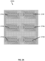
- FIG. 1 shows a quantum Hall resistance device 100 in accordance with aspects of the present disclosure.
- the illustrated quantum Hall resistance device 100 includes a leadless chip carrier 110 and an array of quantum Hall bar elements 130 .
- the leadless chip carrier 110 is connected to the array of quantum Hall bar elements via wires 120 .
- the quantum Hall bar elements 130 are made of graphene, which is epitaxially grown on a substrate.
- the graphene may have a mono layer, which exhibits electrically and optically improved characteristics.
- materials of contacts are made of a superconducting material so that resistance or interconnection resistance between the contacts and the graphene may be significantly reduced.
- the quantum Hall resistance device 100 may include several configurations of the quantum Hall bar elements 130 so as to make a resistance standard in need.
- FIGS. 2 A- 2 C show examples of contact configurations of graphene quantum Hall bar elements in accordance with aspects of the present disclosure.
- the graphene quantum Hall bar element 200 A of FIG. 2 A may include three pairs of graphene bar elements 210 a - 210 f .
- the graphene bar elements 210 a and 210 d are one pair
- the graphene bar elements 210 b and 210 e are another pair
- the graphene bar elements 210 c and 210 f are the other pair.
- Graphene bar elements in each pair are connected in series and three pairs of the graphene bar elements 210 a - 210 f are connected in parallel.
- Each graphene bar element may include six contact positions on the long side and two contact positions on the short side. However, the number of contact positions may vary dependent upon requirements of the resistance standards.
- the graphene quantum Hall bar element 200 B may include three graphene bar elements 220 a - 220 c , which are connected in parallel.
- the graphene quantum Hall bar element 200 C may include three graphene bar elements 230 a - 230 c , which are connected in series.
- FIGS. 2 A- 2 C may be combined in any feasible ways to meet the required resistance standard. Further, the number of graphene bar elements may be increased or decreased, the number of parallel connections or series connections may be increased or decreased to meet the requirements of the resistance standard.
- FIG. 3 A illustrates a diagram of a graphene quantum Hall bar element 300 in accordance with aspects of the present disclosure.
- the graphene quantum Hall bar element 300 may include six contact pads 310 on the long side and two contact pads 310 on the short side. Each contact pad 310 may be split into several branches. As shown in FIG. 3 A , the contact pad 310 has three branches. The split branches of the contact pad 310 may allow for the edge states to equilibrate with the electric potential of the source/drain contacts in the graphene quantum Hall bar element 300 . Further, the split branches play a great role when they represent places where current is injected.
- FIG. 3 B illustrates a diagram of contacts in connection with the graphene quantum Hall bar element 300 of FIG. 3 A in accordance with aspects of the present disclosure.
- the contact pad 310 of the graphene quantum Hall bar element 300 is covered by a protective layer 320 and is connected to contacts 330 .
- the protective layer 320 may be made of a material composed of palladium (Pd) and/or gold (Au). Since the graphene is prone to stick to organic materials, the protective layer 320 prevents the graphene from sticking to organic materials.
- the contacts 330 may be used for any other interconnections and be made of niobium (Nb), titanium (Ti), nitrogen (N), and any combination thereof. Between the superconducting contacts 330 and the graphene, there is no substantial resistance or interconnection resistance, thereby minimizing the unwanted internal resistances while its superconductivity is maintained.
- graphene quantum Hall bar elements as shown in FIGS. 2 A- 2 C may provide large-scale production and stabilization of graphene and provide variable quantized values to be needed or required for resistance standards.
- the contacts 330 becomes a superconductor under the temperature lower than or equal to 12.5 Kelvin (“K”) and under the magnetic flux density lower than or equal to 9 Tesla (“T”).
- K Kelvin
- T 9 Tesla
- the temperature range and the magnetic flux density range are well over the requirements of future precision QHR measurements.
- the superconducting features of the contacts 330 are shown in graph 400 in FIG. 4 .
- the vertical axis of the graph 400 represents resistance in Ohm ( ⁇ ) and the horizontal axis represents temperature in K. Measurement values are plotted in a curve 410 .
- the resistance of the contacts 330 is about 3 ⁇ when the temperature is over 12.5 K, and drops to zero when the temperature is less than or equal to 12.5 K.
- the curve 410 shows transition at 12.5 K and the contacts 330 , which is a combination of niobium (Nb), titanium (Ti), and nitrogen (N), or for example niobium titanium nitride (NbTiN), becomes a superconductor under 12.5 K.
- FIG. 5 Photolithography processes for fabricating a graphene quantum Hall bar element are graphically illustrated from the top illustration to the bottom illustration in FIG. 5 in accordance with aspects of the present disclosure.
- graphene may be epitaxially grown on a substrate 505 , the epitaxial graphene (EG) 510 may then be shielded by a thin layer of palladium 515 and/or gold 520 to allow for contaminant-free graphene/metal contacts.
- the substrate 505 may be a 4H—SiC(0001) semi-insulating substrate with a miscut, relative to the (0001) atomic plane of 4H—SiC(0001), which is less than or equal to 0.10°.
- a mask 525 of palladium and gold may cover the thin gold layer 520 as shown in the second illustration from the top.
- Argon (Ar) gas plasma 530 is used to etch the thin gold layer 520 , the thin palladium layer 515 , and the EG 510 without the portion covered by the mask layer 525 , as shown in the third illustration from the top.
- Niobium titanium nitride (NbTiN) is sputtered to form a contact layer 535 over a portion of the mask layer 525 and portions of the substrate 505 , where the thin gold layer 520 , the thin palladium layer 515 , and the EG 510 have been etched or removed, as shown in the fourth illustration from the top.
- the contact layer 535 may have a thickness of about 340 nm.
- Ti may be sputtered to form an adhesion layer before NbTiN is sputtered, and may have a thickness of about 7.5 nm.
- platinum (Pt) 540 may be sputtered over the contact layer 535 to prevent surface oxidation and have a thickness of about 30 nm.
- a photolithography process is used to open a window to the mask layer 525 .
- Aqua regia or diluted aqua regia 545 is applied to remove the mask layer 525 with the thin palladium layer 515 and the thin gold layer 520 .
- This wet-etching procedure does not harm the EG 510 .
- the only connection portion between the contact layer 535 and the EG 510 constitutes the desired contacts.
- Detailed description of the photolithography process for fabricating a graphene quantum Hall bar element may be found in “Two-Terminal and Multi-Terminal Designs for Next-Generation Quantized Hall Resistance Standards: Contact Material and Geometry,” IEEE Transactions on Electron Devices , Vol. 66, No.
- FIG. 6 A illustrates an example of wire bonding for source/drain resistance measurements of graphene quantum Hall bar elements 600 in accordance with aspects of the present disclosure.
- two graphene quantum Hall bar elements 600 in each pair are connected in series and three pairs of graphene quantum Hall bar elements 600 are connected in parallel.
- Reference points “a” and “b” are source and drain, respectively.
- Reference points “1,” “2,” and “3” are centers of three pairs of graphene quantum Hall bar elements 600 , where potential difference is measured as a function of magnetic flux density.
- the rectangle of each graphene quantum Hall bar element has six contact pads in the length direction and two contact pads in the width direction.
- the rectangular shape of the graphene quantum Hall bar element is 2220 ⁇ m in the length direction and 400 ⁇ m in the width direction.
- the distance between two adjacent contact pads in the length direction is 320 ⁇ m.
- FIG. 6 B illustrates a graph 620 including a boxplot showing measurements for potential differences and voltage errors between pairs of center locations of the graphene quantum Hall bar elements 600 of FIG. 6 A .
- the left vertical axis represents voltage errors in nV/V
- the right vertical axis represents potential differences in nV
- the horizontal axis represents contact pairs.
- the measurements are taken under the magnetic flux density greater than 6 Tesla and the temperature of 1.6 K with current of 1,156 ⁇ A flowing between the source and the drain.
- the boxplot includes three parts 625 a - 625 c , which show measurements at contact pair of “1” and “2,” at contact pair of “2” and “3,” and at contact pair of “1” and “3.”
- the measurements for potential differences between “1” and “2” have a range of potential difference between about 0 and about ⁇ 100 nV and a range of voltage errors between about 0 and ⁇ 20 nV/V.
- FIG. 6 C illustrates a graph 640 showing measurements for source/drain resistances and potential differences between the reference points “1,” “2,” and “3” based on the configuration shown in FIG. 6 A
- the left vertical axis represents a resistance (S/D) between the source and the drain in ⁇
- the right vertical axis represents a potential difference in V
- the horizontal axis represents a magnetic flux density in T.
- Curve 645 a is located in the top in the middle part of the horizontal axis and represents a potential difference between reference points “1” and “2”
- curve 645 b is located in the second from the top in the middle part of the horizontal axis and represents a resistance between the source and the drain
- curve 645 c is located in the third from the top in the middle part of the horizontal axis and represents a potential difference between reference points “1” and “3”
- curve 645 d is located in the bottom in the middle part of the horizontal axis and represents a potential difference between reference points “2 and 3.”
- the S/D resistance or R K is maintained at about 8,604 ⁇ when the magnetic flux density is greater than or equal to about 3.5 T, and the potential differences among “1,” “2,” and “3” based on the curves 645 a , 645 c , and 645 d become zero volts when the magnetic flux density is greater than or equal to about 3.5 T.
- FIG. 7 A illustrates an example of wire bonding for source/drain resistance measurements of a graphene quantum Hall bar elements 700 in accordance with aspects of the present disclosure.
- two graphene quantum Hall bar elements 700 in each pair are connected in series and three pairs of graphene quantum Hall bar elements 700 are connected in parallel.
- Reference points “1” and “2” are source and drain, respectively.
- Reference points “a,” “b,” and “c” are centers of three pairs of graphene quantum Hall bar elements, where potential difference is measured as a function of magnetic flux density.
- the rectangle of each graphene quantum Hall bar element has six contact pads in the length direction and two contact pads in the width direction.
- FIG. 7 B illustrates a graph 720 including a boxplot showing measurements for potential differences and voltage errors between pairs of center locations of the graphene quantum Hall bar elements 700 of FIG. 7 A .
- the left vertical axis represents voltage errors in nV/V
- the right vertical axis represents potential differences in nV
- the horizontal axis represents potential contact pairs.
- the measurements are taken under the magnetic flux density greater than 6 T and the temperature of 1.6 K with current of 771 ⁇ A flowing between the source and the drain.
- the boxplot includes three parts 725 a - 725 c .
- Three parts 725 a - 725 c show measurements at the contact pair of “a” and “b,” at the contact pair of “b” and “c,” and at the contact pair of “a” and “c.”
- the potential difference between “a” and “b” should be zero.
- Hall voltage may occur between “a” and “b”.
- the measurements for potential differences between “a” and “b” have a range of potential difference between about 0 and about 50 nV and a range of voltage errors between about 0 and about 10 nV/V.
- FIG. 7 C illustrates a graph 740 showing measurements for source/drain (S/D) resistances and potential differences between the reference points “a,” “b,” and “c” based on the configuration shown in FIG. 7 A
- the left vertical axis represents the S/D resistance in ⁇
- the right vertical axis represents a potential difference in V
- the horizontal axis represents a magnetic flux density in T.
- Three solid curves represent potential differences in V among reference points “a,” “b,” and “c”
- three dotted curves represent S/D resistances in ⁇ among the three reference points “a,” “b,” and “c.”
- the contacts of the graphene quantum Hall bar elements 700 show superconducting characteristics under the magnetic flux density, which is greater than or equal to 6 T and the temperature, which is equal to 1.6 K.
- FIG. 8 shows a flowchart illustrating a method 800 for fabricating a graphene quantum Hall array resistance device in accordance with aspects of the present disclosure.
- the method 800 starts with providing a substrate in step 810 .
- the substrate may be a silicon carbide (SiC) wafer, which is commonly found as a circular piece about 4 inches in diameter.
- the substrate may be a 4H—SiC(0001) semi-insulating substrate with a miscut, relative to the (0001) atomic plane of the 4H—SiC(0001), which is less than or equal to 0.10°.
- the substrate may be cut into 7.6 mm square chips. After the cutting, the diced chips may be cleansed with piranha etch solution and then further cleansed with diluted hydrofluoric acid (5:1 deionized H 2 O to hydrofluoric acid).
- the chips may be provided with several drops of custom chemical solution at 6000 rpm for 1 min.
- the chemical solution may be composed of 99.8% isopropanol and 0.2% polymer blend as a photoresist, which may be composed of 75% propylene glycol methyl ether acetate, 5% diazonaphthoquinone sulfonic ester, 2% phenolic acid, 18% cresol novolak resin (also known as phenol formaldehyde resin).
- the cresol novolak resin may be important in successful graphene growth.
- step 820 graphene is epitaxially grown on the chips in a furnace.
- the side of the chips identified as the (0001) surface or silicon-face is placed in contact with polished graphite slab to promote homogenous epitaxial graphene growth.
- Step 820 may be performed in small steps as described below.
- step 820 a In the furnace, the chip and the slab are purged with Ar gas in step 820 a .
- Ar gas in the Ar and H 2 environment (about 3% H 2 by volume), temperature is ramped at a rate of about 3° C./s to 500° C. and is maintained at 500° C. for 5 minutes in step 820 b.
- the temperature is also ramped at the same rate to 1050° C. and is maintained at 1050° C. for one hour in step 820 c .
- the gas environment is purified such that only Ar gas remains in the furnace and no more H 2 gas is used.
- the temperature is maintained at 1050° C. for an additional two hours in this purified gas environment.
- step 820 e the temperature is ramped again at the same rate to 1300° C. and is maintained at 1300° C. for one minute. Another ramping temperature is performed at the same rate to 1875° C. and the temperature remains at 1875° C. for 4.5 minutes in step 820 f.
- step 820 g the temperature is now ramped down to room temperature by allowing the furnace to cool overnight. After cooling down, the graphene is epitaxially grown on the chips. Such epitaxial growth may form a mono layer of graphene over the chips.
- the protective layer may be made of Pd and Au. Specifically, for example, 10 nm of Pd may be deposited onto the chips and 15 nm of Au may be also deposited onto the chips using electron beam deposition. The initial pressure of the beam deposition may be about 10 ⁇ 7 Torr.
- step 840 the graphene is etched to make a plurality of quantum Hall bar elements, each including first contact patterns at edge thereof, such as the split branches shown in FIG. 3 B .
- a “lift-off” photoresist is rotated at 4000 rpm for 45 seconds and the rotation speed may be accelerated to 5000 rpm/s in step 840 a .
- the lift-off photoresist may be composed of 75% cyclopentanone, 15% propylene glycol monomethyl ether, and 10% polyaliphatic imide copolymer. Chips are baked immediately after spinning the lift-off photoresist at 170° C. for 5 minutes in step 840 b.
- a “capping” photoresist is rotated at 4500 rpm for 45 seconds and the rotation speed may be accelerated to 5000 rpm/s in step 840 c .
- the capping photoresist may be composed of 75% electronic-grade propylene glycol monomethyl ether acetate, 15% mixed cresol novolak resin, and 10% diazo photoactive compound.
- the chips are baked at 115° C. for 1 minute immediately after spinning the capping photoresist in step 840 d.
- step 840 e the chips are exposed to ultraviolet light, of which wavelength may be 365 nm, for 5 seconds to write a custom shape such as the shape of the graphene quantum Hall bar element 300 of FIG. 3 A or other designs shown in FIGS. 2 A- 2 C .
- This can be performed on a maskless aligner. In an aspect, this can be done with a high-precision mask and bond aligner.
- step 840 f the exposed chips are taken out of the furnace and washed with a solution of 97% water and 3% tetramethylammonium hydroxide for 1 minute. This removes the photoresists exposed to ultraviolet light, leaving a region of palladium/gold-coated graphene exposed to air in the shape of FIG. 3 .
- step 840 g the chips are further washed in deionized H 2 O.
- the chips are dry-etched with argon plasma under pressure of 4 Pascal (Pa) and power of 50 Watts (W) for 30 seconds in step 840 h , and 50 nm of gold is deposited onto the chips in step 840 i.
- step 840 j the chips are placed in 100 mL of N-Methyl-2-pyrrolidone for one hour at 75° C., thereby allowing the remaining photoresists to lift off from the chips.
- step 840 k the chips are dry-etched with argon plasma under pressure of 4 Pa and power of 150 W for 7.5 minutes.
- the steps 840 a through 840 k are repeatedly performed with a photomask in the shape of the first contact patterns, which are shown in FIG. 3 A , in step 840 e.
- the contacts are deposited over the protective layer in step 850 .
- the contacts may be made of any combination of niobium, titanium, and nitrogen. Specifically, 7.5 nm of titanium is deposited, 330 nm of niobium titanium nitride is deposited, and finally 50 nm of platinum as a capping layer is deposited onto the chips using electron beam deposition in step 850 a .
- the initial pressure may be 1.33 ⁇ 10 ⁇ 3 Pa.
- step 850 b the chips are placed in 100 mL bath of N-Methyl-2-pyrrolidone for one hour at 75° C., thereby allowing the remaining photoresists to lift off from the substrate.
- steps 840 c through 840 h are repeated with a photomask design with six rectangles, for example, 2400 ⁇ m in length by 450 ⁇ m in width in step 840 e .
- these six rectangles should be aligned with the six Hall bars shown in FIG. 2 A , such that each of the 2220 ⁇ m by 400 ⁇ m Hall bars have their general rectangular perimeter enclosed within the larger rectangle, while excluding all or part of the split branches or trident features of the contact pads (e.g., the contact pads 310 of FIG. 3 A ).
- the electrical contact pads may not be within this rectangular window.
- the metal/graphene contacts are split into several branches. This split branch design allows for the edge states to equilibrate with the electric potential of the source/drain contacts in the quantum Hall regime.
- the split branches play a role when they represent the point where current is injected.
- step 850 c the chips are submerged in diluted aqua regia, which is composed of 1:1 deionized H 2 O to aqua regia, for 45 seconds.
- Final shapes formed from step 850 c may look like the shape of the contacts 330 in FIG. 3 B .
- the graphene Hall bar may not have any remaining metal.
- the three separated trident metal channels forming the source/drain contacts 330 enable graphene quantum Hall bar elements to perform significantly better due to minimizing the influence of the contact resistance.
- step 850 d the chips are vigorously cleaned with acetone squirt bottle in one minute, and then placed in acetone bath for two hours.
- step 850 e the chips are transferred to isopropanol bath for five minutes.
- the graphene quantum Hall bar elements are formed.
- 200 A, 200 B, or 200 C may be formed after step 850 f.
- a similar carrier density for quantum Hall bar elements may be provided by functionalizing the chips with chromium tricarbonyl using a small deposition furnace.
- Raw material, chromium hexacarbonyl, may be needed.
- Functionalization may be also performed in small steps as follows:
- step 860 a the chamber door is opened and phosphor-bronze boat designed to carry the chips and functionalizing compound are removed.
- step 860 b the chips are loaded into the boat and compound storage pocket is left empty.
- step 860 c the boat is loaded into the furnace chamber.
- step 860 d N2 gas is allowed to flow through the open furnace chamber for a few minutes.
- step 860 e the furnace chamber door is closed and N 2 gas flow is shut off.
- step 860 f the boat is baked at 130° C. for one hour.
- the range of temperature tolerance may be ⁇ 10° C.
- step 860 g After baking, in step 860 g , the same amount of N 2 flow is restarted and used while opening the furnace chamber.
- step 860 h when the furnace chamber door is opened, the boat is removed and 100 mg of chromium hexacarbonyl [Cr(CO) 6 ] is loaded into a designated pocket in the boat.
- the boat is reloaded, the furnace chamber is closed, and the N 2 gas flow is turned off in step 860 h.
- step 860 i while the temperature of the furnace chamber is maintained at 130° C., the pressure of the furnace chamber is decreased to 10 ⁇ 2 Torr for 40 minutes.
- step 860 k the deposition process is complete, and in step 860 l , the chamber heating source is turned off and the furnace chamber is cooled overnight before removing the chips.
- the functionalization may be found in “Gateless and reversible Carrier density tunability in epitaxial graphene devices functionalized with chromium tricarbonyl,” Carbon 142 (2019), pp 468-474, which is hereby incorporated by reference in its entirety.
- the quantum Hall bar resistance apparatus is mounted onto to a leadless chip carrier in step 870 , and wires are bonded between the quantum Hall bar resistance apparatus with the leadless chip carrier.
- the final result may be like the quantum Hall resistance device 100 of FIG. 1 .
- various combination of S/D resistance in terms of the von Klitzing constant of resistance R K may be realized.
- the carrier density may be adjusted by annealing the chip between 300 K and 360 K. Typically, functional devices are annealed at 350 K for 25 minutes.
- the carrier density may be reset to a low value by leaving the chip in air for 24 hours and then annealing the chip between 300 K and 360 K
- the following table shows another aspect of the method 800 .
- Purging and pre-sputtering steps are performed to ensure removal of possible gaseous contaminants in the furnace and on the sputter targets in steps 1 and 2.
- Titanium radio frequency source
- niobium direct current source
- titanium are both sputtered in a nitrogen/argon environment to promote growth of superconducting niobium titanium nitride in step 5.
- platinum is deposited as a protective capping layer in step 8.
- the flow of N 2 gas, Ar gas, the level of RF power, and the output power of a DC source may be controlled as shown below in the table.
- Step 1 2 3 4 5 6 7 8 Time (s) 1200 600 360 300 600 60 300 300 N 2 flow 120 — — 3 3 — — — (cm ⁇ 3 /min) Ar flow 20 50 50 50 50 50 50 50 (cm ⁇ 3 /min) RF Source — 200 100 150 150 — — — (W) DC Source — 2 — 1.5 1.5 — 0.2 0.2 (W)
- the method 800 may be performed in a different way.
- step 820 instead of chemical solution composed of 99.8% isopropanol and 0.2% polymer blend, the chemical solution composed of 0.2% AZ5214E polymer, which is a photoresist, may be used.
- amorphous boron nitride (a-BN) may be used to encapsulate the graphene layer.
- the a-BN layer may form at least 20 nm thickness, which is sufficient to preserve longitudinal resistivity of the graphene layer.
- a-BN use as an encapsulation layer may be found in “Electrical Stabilization of Surface Resistivity in Epitaxial Graphene Systems by Amorphous Boron Nitride Encapsulation,” ACS Omega 2017, vol. 2, pp 2326-2332, which is hereby incorporated by reference in its entirety.
- the rest of the method in use of a-BN is substantially similar to the method 800 as described above.
- a phrase in the form “A or B” means “(A), (B), or (A and B).”
- a phrase in the form “at least one of A, B, or C” means “(A); (B); (C); (A and B); (A and C); (B and C); or (A, B, and C).”
- programming language and “computer program,” as used herein, each include any language used to specify instructions to a computer, and include (but is not limited to) the following languages and their derivatives: Assembler, Basic, Batch files, BCPL, C, C+, C++, Delphi, Fortran, Java, JavaScript, machine code, operating system command languages, Pascal, Perl, PL1, scripting languages, Visual Basic, metalanguages which themselves specify programs, and all first, second, third, fourth, fifth, or further generation computer languages. Also included are database and other data schemas, and any other meta-languages.
- the systems described herein may also utilize one or more controllers to receive various information and transform the received information to generate an output.
- the controller may include any type of computing device, computational circuit, or any type of processor or processing circuit capable of executing a series of instructions that are stored in a memory.
- the controller may include multiple processors and/or multicore central processing units (CPUs) and may include any type of processor, such as a microprocessor, digital signal processor, microcontroller, programmable logic device (PLD), field programmable gate array (FPGA), or the like.
- the controller may also include a memory to store data and/or instructions that, when executed by the one or more processors, causes the one or more processors to perform one or more methods and/or algorithms.
Landscapes
- Physics & Mathematics (AREA)
- General Physics & Mathematics (AREA)
- Condensed Matter Physics & Semiconductors (AREA)
- Engineering & Computer Science (AREA)
- Manufacturing & Machinery (AREA)
- Hall/Mr Elements (AREA)
- Carbon And Carbon Compounds (AREA)
Abstract
Description
| |
1 | 2 | 3 | 4 | 5 | 6 | 7 | 8 |
| Time (s) | 1200 | 600 | 360 | 300 | 600 | 60 | 300 | 300 |
| N2 flow | 120 | — | — | 3 | 3 | — | — | — |
| (cm−3/min) | ||||||||
| |
20 | 50 | 50 | 50 | 50 | 50 | 50 | 50 |
| (cm−3/min) | ||||||||
| RF Source | — | 200 | 100 | 150 | 150 | — | — | — |
| (W) | ||||||||
| DC Source | — | 2 | — | 1.5 | 1.5 | — | 0.2 | 0.2 |
| (W) | ||||||||
Claims (22)
Priority Applications (1)
| Application Number | Priority Date | Filing Date | Title |
|---|---|---|---|
| US17/435,807 US11867775B2 (en) | 2019-03-04 | 2020-03-04 | Systems, devices, and methods for resistance metrology using graphene with superconducting components |
Applications Claiming Priority (3)
| Application Number | Priority Date | Filing Date | Title |
|---|---|---|---|
| US201962813526P | 2019-03-04 | 2019-03-04 | |
| PCT/US2020/020969 WO2020180977A1 (en) | 2019-03-04 | 2020-03-04 | Systems, devices, and methods for resistance metrology using graphene with superconducting components |
| US17/435,807 US11867775B2 (en) | 2019-03-04 | 2020-03-04 | Systems, devices, and methods for resistance metrology using graphene with superconducting components |
Publications (2)
| Publication Number | Publication Date |
|---|---|
| US20220146597A1 US20220146597A1 (en) | 2022-05-12 |
| US11867775B2 true US11867775B2 (en) | 2024-01-09 |
Family
ID=72337993
Family Applications (1)
| Application Number | Title | Priority Date | Filing Date |
|---|---|---|---|
| US17/435,807 Active 2040-03-14 US11867775B2 (en) | 2019-03-04 | 2020-03-04 | Systems, devices, and methods for resistance metrology using graphene with superconducting components |
Country Status (2)
| Country | Link |
|---|---|
| US (1) | US11867775B2 (en) |
| WO (1) | WO2020180977A1 (en) |
Families Citing this family (4)
| Publication number | Priority date | Publication date | Assignee | Title |
|---|---|---|---|---|
| KR102263568B1 (en) * | 2021-02-15 | 2021-06-11 | 한국표준과학연구원 | Encapsulated constructure for quantum resistance standard |
| CN114200373B (en) * | 2021-12-09 | 2022-12-09 | 中国科学院上海微系统与信息技术研究所 | Small quantum resistance standard |
| CN115792381B (en) * | 2022-11-24 | 2023-06-23 | 中国计量科学研究院 | Device and method for precise measurement of load factor using combined quantum Hall resistance |
| EP4589308A1 (en) * | 2024-01-16 | 2025-07-23 | Physikalisch-Technische Bundesanstalt Braunschweig und Berlin | Measuring device for measuring an electrical resistance |
Citations (8)
| Publication number | Priority date | Publication date | Assignee | Title |
|---|---|---|---|---|
| US20090140801A1 (en) * | 2007-11-02 | 2009-06-04 | The Trustees Of Columbia University In The City Of New York | Locally gated graphene nanostructures and methods of making and using |
| US20090303638A1 (en) * | 2008-06-09 | 2009-12-10 | Susumu Ogawa | Magnetoresistance device |
| US20140008616A1 (en) | 2011-03-22 | 2014-01-09 | The University Of Manchester | Transistor device and materials for making |
| US20140179026A1 (en) * | 2012-12-21 | 2014-06-26 | Institute Of Physics, Chinese Academy Of Sciences | Method for generating quantized anomalous hall effect |
| US20150123755A1 (en) * | 2013-11-05 | 2015-05-07 | Tdk Corporation | Magnetization controlling element using magnetoelectric effect |
| EP3106432A1 (en) | 2015-06-18 | 2016-12-21 | Bundesrepublik Deutschland, vertreten durch das Bundesmisterium für Wirtschaft und Energie, endvertreten durch den Präsidenten der PTB | Method for producing graphene |
| US20170229160A1 (en) * | 2016-01-20 | 2017-08-10 | The Johns Hopkins University | Heavy metal multilayers for switching of magnetic unit via electrical current without magnetic field, method and applications |
| KR20170097828A (en) | 2016-02-18 | 2017-08-29 | 나노스 주식회사 | Hall sensor comprising active layer with concave and convex pattern and method of fabricating the hall sensor |
-
2020
- 2020-03-04 US US17/435,807 patent/US11867775B2/en active Active
- 2020-03-04 WO PCT/US2020/020969 patent/WO2020180977A1/en not_active Ceased
Patent Citations (8)
| Publication number | Priority date | Publication date | Assignee | Title |
|---|---|---|---|---|
| US20090140801A1 (en) * | 2007-11-02 | 2009-06-04 | The Trustees Of Columbia University In The City Of New York | Locally gated graphene nanostructures and methods of making and using |
| US20090303638A1 (en) * | 2008-06-09 | 2009-12-10 | Susumu Ogawa | Magnetoresistance device |
| US20140008616A1 (en) | 2011-03-22 | 2014-01-09 | The University Of Manchester | Transistor device and materials for making |
| US20140179026A1 (en) * | 2012-12-21 | 2014-06-26 | Institute Of Physics, Chinese Academy Of Sciences | Method for generating quantized anomalous hall effect |
| US20150123755A1 (en) * | 2013-11-05 | 2015-05-07 | Tdk Corporation | Magnetization controlling element using magnetoelectric effect |
| EP3106432A1 (en) | 2015-06-18 | 2016-12-21 | Bundesrepublik Deutschland, vertreten durch das Bundesmisterium für Wirtschaft und Energie, endvertreten durch den Präsidenten der PTB | Method for producing graphene |
| US20170229160A1 (en) * | 2016-01-20 | 2017-08-10 | The Johns Hopkins University | Heavy metal multilayers for switching of magnetic unit via electrical current without magnetic field, method and applications |
| KR20170097828A (en) | 2016-02-18 | 2017-08-29 | 나노스 주식회사 | Hall sensor comprising active layer with concave and convex pattern and method of fabricating the hall sensor |
Non-Patent Citations (23)
| Title |
|---|
| "Critical Magnetic Fields for Superconductors" retrieved online <https://hyperphysics.phy-astr.gsu.edu/hbase/Solids/scbc.html>, (Jan. 2019), pp. 1-4. |
| Calado, et al., "Ballistic Josephson junctions in edge-contacted graphene", Nature Nanotechnology, Sep. 2015, pp. 761-765, No. 10 (5 pages). |
| Che et al., "Retained Carrier-Mobility and Enhanced Plasmonic-Photovoltaics of Graphene via ring-centered n6 Functionalization and Nanointerfacing", Nano Letters, 2017, pp. 4381-4389, No. 17 (9 pages). |
| De Heer, et al. "Large area and structured epitaxial graphene produced by confinement controlled ublimation of silicon carbide", PNAS, Oct. 11, 2011, pp. 16900-16905, vol. 108, No. 41 (6 pages). |
| Di Bartolomeo, A. et al., "Graphene field effect transistors with niobium contacts and asymmetric transfer characteristics" Nanotechnology (Nov. 2015) pp. 1-19, vol. 26, issue 47. |
| He et al., "Polymer-encapsulated molecular doped epigraphene for quantum resistance metrology", Metrologia, 2019, pp. 1-9, No. 56 (10 pages). |
| International Search Report issued in corresponding International Application No. PCT/US2020/020969, dated May 28, 2020, pp. 1-12. |
| Kruskopf et al., "Epitaxial graphene for quantum resistance metrology", Metrologia, 2018, pp. R27-R36, No. 55 (11 pages). |
| Kruskopf et al., "Two-Terminal and Multi-Terminal Designs for Next-Generation Quantized Hall Resistance Standards: Contact Material and Geometry", IEEE Transactions on Electron Devices, Sep. 2019, pp. 3973-3977, vol. 66, No. 9 (5 pages). |
| Kruskopf, et al., "Comeback of epitaxial graphene for electronics: large-area growth of bilayer-free graphene on SiC", 2D Materials, 2016, pp. 1-9, No. 3, IOP Publishing (10 pages). |
| Kruskopf, et al., "Next-generation crossover-free quantum Hall arrays with superconducting interconnections", Metrologia, 2019, pp. 1-11, No. 56(6) (12 pages). |
| Lafont, F. et al., "Quantum Hall resistance standards from graphene grown by chemical vapour deposition on silicon carbide" Nature Communications (Apr. 2015) pp. 1-9. |
| Lartsev, et al., "A prototype of RK/200 quantum Hall array resistance standard on epitaxial graphene", Journal of Applied Physics, Jul. 29, 2015, pp. 44506-44506-6, No. 118, AIP Publishing (7 pages). |
| Lee, et al., "Proximity coupling in superconductor-graphene heterostructures", Department of Physics, Harvard University (58 pages); (also published in Reports on Progress in Physics, Mar. 28, 2018, No. 81, IOPScience). |
| Real, et al., "Graphene Epitaxial Growth on SiC(0001) for Resistance Standards", IEEE Transactions on Instrumentation and Measurement, Jun. 2013, pp. 1454-1460, vol. 62, No. 6 (7 pages). |
| Rickhaus et al., "Quantum Hall Effect in Graphene with Superconducting Electrodes", Nano Letters, 2012, 1942-1945, vol. 12, American Chemical Society (4 pages). |
| Rigosi et al., "Electrical Stabilization of Surface Resistivity in Epitaxial Graphene Systems by Amorphous Boron Nitride Encapsulation", ACS Omega, 2017, pp. 2326-2332, No. 2 (7 pages). |
| Rigosi et all., "Gateless and reversible Carrier density tunability in epitaxial graphene devices functionalized with chromium tricarbonyl", Carbon,, 2019, pp. 468-474, No. 142 (7 pages). |
| Rigosi, et al., "A Table-Top Graphene Quantized Hall Standard", IEEE Trans. Instrument Measurements, 2019, pp. 1-2 (2 pages). |
| Sarkar et al., "Organometallic Hexahapto Functionalization of Single Layer Graphene as a Route to High Mobility Graphene Devices", Adv. Mater., 2013, pp. 1131-1136, vol. 15, WILEY-VCH Verlag Gmbh & Co. (6 pages). |
| Yang et al., "Epitaxial graphene homogeneity and quantum Hall effect in millimeter-scale devices", Carbon, 2017, pp. 229-236, No. 115, Elsevier Ltd. (8 pages). |
| Yang et al., "Low Carrier Density Epitaxial Graphene Devices on SiC", Small Nano Micro, 2014, pp. 1-6, vol. 11, Issue 1, Wiley-VCH Verlag GmbH & Co. (6 pages). |
| Yu, et al. "New synthesis method for the growth of epitaxial graphene", Journal of Electron Spectroscopy and Related Phenomena, 2011, pp. 100-106, vol. 184, Elsevier B.V. (7 pages). |
Also Published As
| Publication number | Publication date |
|---|---|
| WO2020180977A1 (en) | 2020-09-10 |
| US20220146597A1 (en) | 2022-05-12 |
Similar Documents
| Publication | Publication Date | Title |
|---|---|---|
| US11867775B2 (en) | Systems, devices, and methods for resistance metrology using graphene with superconducting components | |
| CN110462857B (en) | Systems and methods for fabricating superconducting integrated circuits | |
| US11923203B2 (en) | Semiconductor device and method of manufacturing semiconductor device | |
| US10032637B2 (en) | Sacrificial shorting straps for superconducting qubits | |
| US20210351344A1 (en) | Methods for forming structures for mram applications | |
| CN111211165B (en) | A quantum chip three-dimensional structure and its manufacturing and packaging method | |
| US6204102B1 (en) | Method of fabricating compound semiconductor devices using lift-off of insulating film | |
| US11621393B2 (en) | Top buffer layer for magnetic tunnel junction application | |
| JP3351383B2 (en) | Method for manufacturing semiconductor device | |
| JP2008118087A (en) | Method for forming T-gate of high electron mobility transistor and gate structure thereof | |
| WO1997008744A1 (en) | Laminate for forming ohmic electrode and ohmic electrode | |
| JPH0653241A (en) | Method for manufacturing field effect transistor | |
| TW559903B (en) | Semiconductor device and method for fabricating the same | |
| US20240213352A1 (en) | Graphene device and method of fabricating a graphene device | |
| KR960000360B1 (en) | Low contact resistance process | |
| RU2686863C1 (en) | Method of forming t-shaped gate | |
| JP6783463B2 (en) | Diamond semiconductor device, logic device using it, and manufacturing method of diamond semiconductor device | |
| Sugiura et al. | Characterization and surface cleaning technique for MOCVD growth-interrupted GaAs films | |
| EP0108910B1 (en) | Method of forming a passivated compound semiconductor substrate | |
| JPS6292327A (en) | Semiconductor device and manufacture thereof | |
| Mechold et al. | Towards fabrication of sub-micrometer cross-type aluminum Josephson junctions | |
| EP4704540A1 (en) | Quantum device and method of manufacturing quantum device | |
| Cheng et al. | In situ Al $ _2 $ O $ _3 $ passivation of epitaxial tantalum and aluminum films enables long-term stability in superconducting microwave resonators | |
| CN117832095A (en) | A one-dimensional electron gas device based on strontium titanate and its preparation method | |
| Erofeev et al. | A gold free fully copper metalized GaAs pHEMT for the high frequency applications |
Legal Events
| Date | Code | Title | Description |
|---|---|---|---|
| FEPP | Fee payment procedure |
Free format text: ENTITY STATUS SET TO UNDISCOUNTED (ORIGINAL EVENT CODE: BIG.); ENTITY STATUS OF PATENT OWNER: LARGE ENTITY |
|
| FEPP | Fee payment procedure |
Free format text: ENTITY STATUS SET TO SMALL (ORIGINAL EVENT CODE: SMAL); ENTITY STATUS OF PATENT OWNER: LARGE ENTITY |
|
| STPP | Information on status: patent application and granting procedure in general |
Free format text: DOCKETED NEW CASE - READY FOR EXAMINATION |
|
| AS | Assignment |
Owner name: GOVERNMENT OF THE UNITED STATES OF AMERICA, AS REPRESENTED BY THE SECRETARY OF COMMERCE, MARYLAND Free format text: ASSIGNMENT OF ASSIGNORS INTEREST;ASSIGNORS:ELMQUIST, RANDOLPH;RIGOSI, ALBERT;SIGNING DATES FROM 20220927 TO 20220929;REEL/FRAME:061253/0421 |
|
| STPP | Information on status: patent application and granting procedure in general |
Free format text: NOTICE OF ALLOWANCE MAILED -- APPLICATION RECEIVED IN OFFICE OF PUBLICATIONS |
|
| STPP | Information on status: patent application and granting procedure in general |
Free format text: DOCKETED NEW CASE - READY FOR EXAMINATION |
|
| STPP | Information on status: patent application and granting procedure in general |
Free format text: NOTICE OF ALLOWANCE MAILED -- APPLICATION RECEIVED IN OFFICE OF PUBLICATIONS |
|
| FEPP | Fee payment procedure |
Free format text: ENTITY STATUS SET TO UNDISCOUNTED (ORIGINAL EVENT CODE: BIG.); ENTITY STATUS OF PATENT OWNER: LARGE ENTITY |
|
| STPP | Information on status: patent application and granting procedure in general |
Free format text: NOTICE OF ALLOWANCE MAILED -- APPLICATION RECEIVED IN OFFICE OF PUBLICATIONS |
|
| AS | Assignment |
Owner name: UNIVERSITY OF MARYLAND, COLLEGE PARK, MARYLAND Free format text: ASSIGNMENT OF ASSIGNORS INTEREST;ASSIGNOR:KRUSKOPF, MATTIAS;REEL/FRAME:066581/0612 Effective date: 20230825 Owner name: UNIVERSITY OF MARYLAND, COLLEGE PARK, MARYLAND Free format text: ASSIGNMENT OF ASSIGNORS INTEREST;ASSIGNOR:KRUSKOPF, MATTIAS;REEL/FRAME:065610/0580 Effective date: 20230825 |
|
| STPP | Information on status: patent application and granting procedure in general |
Free format text: PUBLICATIONS -- ISSUE FEE PAYMENT RECEIVED |
|
| STPP | Information on status: patent application and granting procedure in general |
Free format text: PUBLICATIONS -- ISSUE FEE PAYMENT VERIFIED |
|
| STCF | Information on status: patent grant |
Free format text: PATENTED CASE |