US11864394B2 - Semiconductor device - Google Patents
Semiconductor device Download PDFInfo
- Publication number
- US11864394B2 US11864394B2 US17/494,534 US202117494534A US11864394B2 US 11864394 B2 US11864394 B2 US 11864394B2 US 202117494534 A US202117494534 A US 202117494534A US 11864394 B2 US11864394 B2 US 11864394B2
- Authority
- US
- United States
- Prior art keywords
- memory cells
- polarity
- memory
- variable resistance
- semiconductor device
- Prior art date
- Legal status (The legal status is an assumption and is not a legal conclusion. Google has not performed a legal analysis and makes no representation as to the accuracy of the status listed.)
- Active, expires
Links
- 239000004065 semiconductor Substances 0.000 title claims abstract description 49
- 230000015654 memory Effects 0.000 claims abstract description 282
- IJGRMHOSHXDMSA-UHFFFAOYSA-N Atomic nitrogen Chemical compound N#N IJGRMHOSHXDMSA-UHFFFAOYSA-N 0.000 claims description 20
- 229910052757 nitrogen Inorganic materials 0.000 claims description 10
- 238000010586 diagram Methods 0.000 description 18
- 238000003860 storage Methods 0.000 description 16
- 238000000034 method Methods 0.000 description 15
- 239000000463 material Substances 0.000 description 14
- 238000004891 communication Methods 0.000 description 10
- PXHVJJICTQNCMI-UHFFFAOYSA-N Nickel Chemical compound [Ni] PXHVJJICTQNCMI-UHFFFAOYSA-N 0.000 description 9
- 230000006870 function Effects 0.000 description 8
- 238000012545 processing Methods 0.000 description 8
- 229910052581 Si3N4 Inorganic materials 0.000 description 6
- BASFCYQUMIYNBI-UHFFFAOYSA-N platinum Chemical compound [Pt] BASFCYQUMIYNBI-UHFFFAOYSA-N 0.000 description 6
- 230000014759 maintenance of location Effects 0.000 description 5
- VYPSYNLAJGMNEJ-UHFFFAOYSA-N Silicium dioxide Chemical compound O=[Si]=O VYPSYNLAJGMNEJ-UHFFFAOYSA-N 0.000 description 4
- GWEVSGVZZGPLCZ-UHFFFAOYSA-N Titan oxide Chemical compound O=[Ti]=O GWEVSGVZZGPLCZ-UHFFFAOYSA-N 0.000 description 4
- 239000010949 copper Substances 0.000 description 4
- 229910000449 hafnium oxide Inorganic materials 0.000 description 4
- 238000004519 manufacturing process Methods 0.000 description 4
- TWNQGVIAIRXVLR-UHFFFAOYSA-N oxo(oxoalumanyloxy)alumane Chemical compound O=[Al]O[Al]=O TWNQGVIAIRXVLR-UHFFFAOYSA-N 0.000 description 4
- BPUBBGLMJRNUCC-UHFFFAOYSA-N oxygen(2-);tantalum(5+) Chemical compound [O-2].[O-2].[O-2].[O-2].[O-2].[Ta+5].[Ta+5] BPUBBGLMJRNUCC-UHFFFAOYSA-N 0.000 description 4
- RVTZCBVAJQQJTK-UHFFFAOYSA-N oxygen(2-);zirconium(4+) Chemical compound [O-2].[O-2].[Zr+4] RVTZCBVAJQQJTK-UHFFFAOYSA-N 0.000 description 4
- 229910021420 polycrystalline silicon Inorganic materials 0.000 description 4
- 229920005591 polysilicon Polymers 0.000 description 4
- 229910052814 silicon oxide Inorganic materials 0.000 description 4
- 229910001936 tantalum oxide Inorganic materials 0.000 description 4
- 239000010936 titanium Substances 0.000 description 4
- OGIDPMRJRNCKJF-UHFFFAOYSA-N titanium oxide Inorganic materials [Ti]=O OGIDPMRJRNCKJF-UHFFFAOYSA-N 0.000 description 4
- 229910052721 tungsten Inorganic materials 0.000 description 4
- 239000010937 tungsten Substances 0.000 description 4
- 229910001928 zirconium oxide Inorganic materials 0.000 description 4
- OKTJSMMVPCPJKN-UHFFFAOYSA-N Carbon Chemical compound [C] OKTJSMMVPCPJKN-UHFFFAOYSA-N 0.000 description 3
- 229910052799 carbon Inorganic materials 0.000 description 3
- 238000013500 data storage Methods 0.000 description 3
- 229910052759 nickel Inorganic materials 0.000 description 3
- 230000003252 repetitive effect Effects 0.000 description 3
- RYGMFSIKBFXOCR-UHFFFAOYSA-N Copper Chemical compound [Cu] RYGMFSIKBFXOCR-UHFFFAOYSA-N 0.000 description 2
- ZOKXTWBITQBERF-UHFFFAOYSA-N Molybdenum Chemical compound [Mo] ZOKXTWBITQBERF-UHFFFAOYSA-N 0.000 description 2
- KJTLSVCANCCWHF-UHFFFAOYSA-N Ruthenium Chemical compound [Ru] KJTLSVCANCCWHF-UHFFFAOYSA-N 0.000 description 2
- 229910010421 TiNx Inorganic materials 0.000 description 2
- RTAQQCXQSZGOHL-UHFFFAOYSA-N Titanium Chemical compound [Ti] RTAQQCXQSZGOHL-UHFFFAOYSA-N 0.000 description 2
- NRTOMJZYCJJWKI-UHFFFAOYSA-N Titanium nitride Chemical compound [Ti]#N NRTOMJZYCJJWKI-UHFFFAOYSA-N 0.000 description 2
- HMDDXIMCDZRSNE-UHFFFAOYSA-N [C].[Si] Chemical compound [C].[Si] HMDDXIMCDZRSNE-UHFFFAOYSA-N 0.000 description 2
- UGACIEPFGXRWCH-UHFFFAOYSA-N [Si].[Ti] Chemical compound [Si].[Ti] UGACIEPFGXRWCH-UHFFFAOYSA-N 0.000 description 2
- RVSGESPTHDDNTH-UHFFFAOYSA-N alumane;tantalum Chemical compound [AlH3].[Ta] RVSGESPTHDDNTH-UHFFFAOYSA-N 0.000 description 2
- UQZIWOQVLUASCR-UHFFFAOYSA-N alumane;titanium Chemical compound [AlH3].[Ti] UQZIWOQVLUASCR-UHFFFAOYSA-N 0.000 description 2
- 230000004888 barrier function Effects 0.000 description 2
- 230000005540 biological transmission Effects 0.000 description 2
- 229910017052 cobalt Inorganic materials 0.000 description 2
- 239000010941 cobalt Substances 0.000 description 2
- GUTLYIVDDKVIGB-UHFFFAOYSA-N cobalt atom Chemical compound [Co] GUTLYIVDDKVIGB-UHFFFAOYSA-N 0.000 description 2
- 239000004020 conductor Substances 0.000 description 2
- 229910052802 copper Inorganic materials 0.000 description 2
- 239000003989 dielectric material Substances 0.000 description 2
- WIHZLLGSGQNAGK-UHFFFAOYSA-N hafnium(4+);oxygen(2-) Chemical compound [O-2].[O-2].[Hf+4] WIHZLLGSGQNAGK-UHFFFAOYSA-N 0.000 description 2
- 239000011572 manganese Substances 0.000 description 2
- 229910052751 metal Inorganic materials 0.000 description 2
- 239000002184 metal Substances 0.000 description 2
- 229910052750 molybdenum Inorganic materials 0.000 description 2
- 239000011733 molybdenum Substances 0.000 description 2
- 150000004767 nitrides Chemical class 0.000 description 2
- 229910052697 platinum Inorganic materials 0.000 description 2
- 229910052707 ruthenium Inorganic materials 0.000 description 2
- 239000011669 selenium Substances 0.000 description 2
- HBMJWWWQQXIZIP-UHFFFAOYSA-N silicon carbide Chemical compound [Si+]#[C-] HBMJWWWQQXIZIP-UHFFFAOYSA-N 0.000 description 2
- HQVNEWCFYHHQES-UHFFFAOYSA-N silicon nitride Chemical compound N12[Si]34N5[Si]62N3[Si]51N64 HQVNEWCFYHHQES-UHFFFAOYSA-N 0.000 description 2
- HWEYZGSCHQNNEH-UHFFFAOYSA-N silicon tantalum Chemical compound [Si].[Ta] HWEYZGSCHQNNEH-UHFFFAOYSA-N 0.000 description 2
- 239000007787 solid Substances 0.000 description 2
- 229910052715 tantalum Inorganic materials 0.000 description 2
- GUVRBAGPIYLISA-UHFFFAOYSA-N tantalum atom Chemical compound [Ta] GUVRBAGPIYLISA-UHFFFAOYSA-N 0.000 description 2
- MZLGASXMSKOWSE-UHFFFAOYSA-N tantalum nitride Chemical compound [Ta]#N MZLGASXMSKOWSE-UHFFFAOYSA-N 0.000 description 2
- JBQYATWDVHIOAR-UHFFFAOYSA-N tellanylidenegermanium Chemical compound [Te]=[Ge] JBQYATWDVHIOAR-UHFFFAOYSA-N 0.000 description 2
- 229910052719 titanium Inorganic materials 0.000 description 2
- 238000012546 transfer Methods 0.000 description 2
- WFKWXMTUELFFGS-UHFFFAOYSA-N tungsten Chemical compound [W] WFKWXMTUELFFGS-UHFFFAOYSA-N 0.000 description 2
- WQJQOUPTWCFRMM-UHFFFAOYSA-N tungsten disilicide Chemical compound [Si]#[W]#[Si] WQJQOUPTWCFRMM-UHFFFAOYSA-N 0.000 description 2
- -1 tungsten nitride Chemical class 0.000 description 2
- 229910021342 tungsten silicide Inorganic materials 0.000 description 2
- ZOXJGFHDIHLPTG-UHFFFAOYSA-N Boron Chemical compound [B] ZOXJGFHDIHLPTG-UHFFFAOYSA-N 0.000 description 1
- GYHNNYVSQQEPJS-UHFFFAOYSA-N Gallium Chemical compound [Ga] GYHNNYVSQQEPJS-UHFFFAOYSA-N 0.000 description 1
- PWHULOQIROXLJO-UHFFFAOYSA-N Manganese Chemical compound [Mn] PWHULOQIROXLJO-UHFFFAOYSA-N 0.000 description 1
- BUGBHKTXTAQXES-UHFFFAOYSA-N Selenium Chemical compound [Se] BUGBHKTXTAQXES-UHFFFAOYSA-N 0.000 description 1
- XUIMIQQOPSSXEZ-UHFFFAOYSA-N Silicon Chemical compound [Si] XUIMIQQOPSSXEZ-UHFFFAOYSA-N 0.000 description 1
- BQCADISMDOOEFD-UHFFFAOYSA-N Silver Chemical compound [Ag] BQCADISMDOOEFD-UHFFFAOYSA-N 0.000 description 1
- NINIDFKCEFEMDL-UHFFFAOYSA-N Sulfur Chemical compound [S] NINIDFKCEFEMDL-UHFFFAOYSA-N 0.000 description 1
- ATJFFYVFTNAWJD-UHFFFAOYSA-N Tin Chemical compound [Sn] ATJFFYVFTNAWJD-UHFFFAOYSA-N 0.000 description 1
- 238000004458 analytical method Methods 0.000 description 1
- 229910052787 antimony Inorganic materials 0.000 description 1
- WATWJIUSRGPENY-UHFFFAOYSA-N antimony atom Chemical compound [Sb] WATWJIUSRGPENY-UHFFFAOYSA-N 0.000 description 1
- 229910052785 arsenic Inorganic materials 0.000 description 1
- RQNWIZPPADIBDY-UHFFFAOYSA-N arsenic atom Chemical compound [As] RQNWIZPPADIBDY-UHFFFAOYSA-N 0.000 description 1
- 229910052797 bismuth Inorganic materials 0.000 description 1
- JCXGWMGPZLAOME-UHFFFAOYSA-N bismuth atom Chemical compound [Bi] JCXGWMGPZLAOME-UHFFFAOYSA-N 0.000 description 1
- 229910052796 boron Inorganic materials 0.000 description 1
- 150000004770 chalcogenides Chemical class 0.000 description 1
- 230000003247 decreasing effect Effects 0.000 description 1
- 238000005137 deposition process Methods 0.000 description 1
- 238000013461 design Methods 0.000 description 1
- 238000005516 engineering process Methods 0.000 description 1
- 238000000605 extraction Methods 0.000 description 1
- 238000007667 floating Methods 0.000 description 1
- 229910052733 gallium Inorganic materials 0.000 description 1
- 229910052732 germanium Inorganic materials 0.000 description 1
- GNPVGFCGXDBREM-UHFFFAOYSA-N germanium atom Chemical compound [Ge] GNPVGFCGXDBREM-UHFFFAOYSA-N 0.000 description 1
- 229910052738 indium Inorganic materials 0.000 description 1
- APFVFJFRJDLVQX-UHFFFAOYSA-N indium atom Chemical compound [In] APFVFJFRJDLVQX-UHFFFAOYSA-N 0.000 description 1
- 230000007774 longterm Effects 0.000 description 1
- 229910052748 manganese Inorganic materials 0.000 description 1
- 229910052711 selenium Inorganic materials 0.000 description 1
- 229910052710 silicon Inorganic materials 0.000 description 1
- 239000010703 silicon Substances 0.000 description 1
- 229910052709 silver Inorganic materials 0.000 description 1
- 239000004332 silver Substances 0.000 description 1
- 230000003068 static effect Effects 0.000 description 1
- 229910052717 sulfur Inorganic materials 0.000 description 1
- 239000011593 sulfur Substances 0.000 description 1
- 238000004381 surface treatment Methods 0.000 description 1
- 229910052714 tellurium Inorganic materials 0.000 description 1
- PORWMNRCUJJQNO-UHFFFAOYSA-N tellurium atom Chemical compound [Te] PORWMNRCUJJQNO-UHFFFAOYSA-N 0.000 description 1
- 230000000007 visual effect Effects 0.000 description 1
Images


Classifications
-
- H—ELECTRICITY
- H10—SEMICONDUCTOR DEVICES; ELECTRIC SOLID-STATE DEVICES NOT OTHERWISE PROVIDED FOR
- H10N—ELECTRIC SOLID-STATE DEVICES NOT OTHERWISE PROVIDED FOR
- H10N70/00—Solid-state devices without a potential-jump barrier or surface barrier, and specially adapted for rectifying, amplifying, oscillating or switching
- H10N70/801—Constructional details of multistable switching devices
- H10N70/821—Device geometry
- H10N70/826—Device geometry adapted for essentially vertical current flow, e.g. sandwich or pillar type devices
-
- H—ELECTRICITY
- H10—SEMICONDUCTOR DEVICES; ELECTRIC SOLID-STATE DEVICES NOT OTHERWISE PROVIDED FOR
- H10B—ELECTRONIC MEMORY DEVICES
- H10B63/00—Resistance change memory devices, e.g. resistive RAM [ReRAM] devices
- H10B63/80—Arrangements comprising multiple bistable or multi-stable switching components of the same type on a plane parallel to the substrate, e.g. cross-point arrays
- H10B63/84—Arrangements comprising multiple bistable or multi-stable switching components of the same type on a plane parallel to the substrate, e.g. cross-point arrays arranged in a direction perpendicular to the substrate, e.g. 3D cell arrays
-
- G—PHYSICS
- G11—INFORMATION STORAGE
- G11C—STATIC STORES
- G11C13/00—Digital stores characterised by the use of storage elements not covered by groups G11C11/00, G11C23/00, or G11C25/00
- G11C13/0002—Digital stores characterised by the use of storage elements not covered by groups G11C11/00, G11C23/00, or G11C25/00 using resistive RAM [RRAM] elements
- G11C13/0021—Auxiliary circuits
- G11C13/003—Cell access
-
- G—PHYSICS
- G11—INFORMATION STORAGE
- G11C—STATIC STORES
- G11C13/00—Digital stores characterised by the use of storage elements not covered by groups G11C11/00, G11C23/00, or G11C25/00
- G11C13/0002—Digital stores characterised by the use of storage elements not covered by groups G11C11/00, G11C23/00, or G11C25/00 using resistive RAM [RRAM] elements
- G11C13/0004—Digital stores characterised by the use of storage elements not covered by groups G11C11/00, G11C23/00, or G11C25/00 using resistive RAM [RRAM] elements comprising amorphous/crystalline phase transition cells
-
- G—PHYSICS
- G11—INFORMATION STORAGE
- G11C—STATIC STORES
- G11C13/00—Digital stores characterised by the use of storage elements not covered by groups G11C11/00, G11C23/00, or G11C25/00
- G11C13/0002—Digital stores characterised by the use of storage elements not covered by groups G11C11/00, G11C23/00, or G11C25/00 using resistive RAM [RRAM] elements
- G11C13/0021—Auxiliary circuits
- G11C13/004—Reading or sensing circuits or methods
-
- G—PHYSICS
- G11—INFORMATION STORAGE
- G11C—STATIC STORES
- G11C13/00—Digital stores characterised by the use of storage elements not covered by groups G11C11/00, G11C23/00, or G11C25/00
- G11C13/0002—Digital stores characterised by the use of storage elements not covered by groups G11C11/00, G11C23/00, or G11C25/00 using resistive RAM [RRAM] elements
- G11C13/0021—Auxiliary circuits
- G11C13/0061—Timing circuits or methods
-
- G—PHYSICS
- G11—INFORMATION STORAGE
- G11C—STATIC STORES
- G11C13/00—Digital stores characterised by the use of storage elements not covered by groups G11C11/00, G11C23/00, or G11C25/00
- G11C13/0002—Digital stores characterised by the use of storage elements not covered by groups G11C11/00, G11C23/00, or G11C25/00 using resistive RAM [RRAM] elements
- G11C13/0021—Auxiliary circuits
- G11C13/0069—Writing or programming circuits or methods
-
- G—PHYSICS
- G11—INFORMATION STORAGE
- G11C—STATIC STORES
- G11C5/00—Details of stores covered by group G11C11/00
- G11C5/06—Arrangements for interconnecting storage elements electrically, e.g. by wiring
- G11C5/063—Voltage and signal distribution in integrated semi-conductor memory access lines, e.g. word-line, bit-line, cross-over resistance, propagation delay
-
- H—ELECTRICITY
- H10—SEMICONDUCTOR DEVICES; ELECTRIC SOLID-STATE DEVICES NOT OTHERWISE PROVIDED FOR
- H10B—ELECTRONIC MEMORY DEVICES
- H10B61/00—Magnetic memory devices, e.g. magnetoresistive RAM [MRAM] devices
-
- H—ELECTRICITY
- H10—SEMICONDUCTOR DEVICES; ELECTRIC SOLID-STATE DEVICES NOT OTHERWISE PROVIDED FOR
- H10N—ELECTRIC SOLID-STATE DEVICES NOT OTHERWISE PROVIDED FOR
- H10N70/00—Solid-state devices without a potential-jump barrier or surface barrier, and specially adapted for rectifying, amplifying, oscillating or switching
- H10N70/20—Multistable switching devices, e.g. memristors
- H10N70/231—Multistable switching devices, e.g. memristors based on solid-state phase change, e.g. between amorphous and crystalline phases, Ovshinsky effect
-
- H—ELECTRICITY
- H10—SEMICONDUCTOR DEVICES; ELECTRIC SOLID-STATE DEVICES NOT OTHERWISE PROVIDED FOR
- H10N—ELECTRIC SOLID-STATE DEVICES NOT OTHERWISE PROVIDED FOR
- H10N70/00—Solid-state devices without a potential-jump barrier or surface barrier, and specially adapted for rectifying, amplifying, oscillating or switching
- H10N70/801—Constructional details of multistable switching devices
- H10N70/841—Electrodes
-
- G—PHYSICS
- G11—INFORMATION STORAGE
- G11C—STATIC STORES
- G11C13/00—Digital stores characterised by the use of storage elements not covered by groups G11C11/00, G11C23/00, or G11C25/00
- G11C13/0002—Digital stores characterised by the use of storage elements not covered by groups G11C11/00, G11C23/00, or G11C25/00 using resistive RAM [RRAM] elements
- G11C13/0021—Auxiliary circuits
- G11C13/004—Reading or sensing circuits or methods
- G11C2013/0052—Read process characterized by the shape, e.g. form, length, amplitude of the read pulse
-
- G—PHYSICS
- G11—INFORMATION STORAGE
- G11C—STATIC STORES
- G11C13/00—Digital stores characterised by the use of storage elements not covered by groups G11C11/00, G11C23/00, or G11C25/00
- G11C13/0002—Digital stores characterised by the use of storage elements not covered by groups G11C11/00, G11C23/00, or G11C25/00 using resistive RAM [RRAM] elements
- G11C13/0021—Auxiliary circuits
- G11C13/0069—Writing or programming circuits or methods
- G11C2013/0092—Write characterized by the shape, e.g. form, length, amplitude of the write pulse
-
- G—PHYSICS
- G11—INFORMATION STORAGE
- G11C—STATIC STORES
- G11C2213/00—Indexing scheme relating to G11C13/00 for features not covered by this group
- G11C2213/70—Resistive array aspects
- G11C2213/71—Three dimensional array
-
- Y—GENERAL TAGGING OF NEW TECHNOLOGICAL DEVELOPMENTS; GENERAL TAGGING OF CROSS-SECTIONAL TECHNOLOGIES SPANNING OVER SEVERAL SECTIONS OF THE IPC; TECHNICAL SUBJECTS COVERED BY FORMER USPC CROSS-REFERENCE ART COLLECTIONS [XRACs] AND DIGESTS
- Y02—TECHNOLOGIES OR APPLICATIONS FOR MITIGATION OR ADAPTATION AGAINST CLIMATE CHANGE
- Y02D—CLIMATE CHANGE MITIGATION TECHNOLOGIES IN INFORMATION AND COMMUNICATION TECHNOLOGIES [ICT], I.E. INFORMATION AND COMMUNICATION TECHNOLOGIES AIMING AT THE REDUCTION OF THEIR OWN ENERGY USE
- Y02D10/00—Energy efficient computing, e.g. low power processors, power management or thermal management
Definitions
- the present disclosure relates to an electronic device, and more particularly, to a semiconductor device.
- a semiconductor device capable of storing information in various electronic devices such as a computer and a portable communication device has been demanded, according to miniaturization, low power consumption, high performance, and diversification of an electronic device. Therefore, study on a semiconductor device capable of storing data by using a switching characteristic between different resistance states according to an applied voltage or current.
- Examples of such a semiconductor device include a resistive random access memory (RRAM), a phase-change random access memory (PRAM), a ferroelectric random access memory (FRAM), a magnetic random access memory (MRAM), an e-fuse, and the like.
- a semiconductor device may include first row lines each extending in a first direction, column lines each extending in a second direction crossing the first direction, second row lines each extending in the first direction, a plurality of first memory cells respectively coupled between the first row lines and the column lines, each of the plurality of first memory cells including a first variable resistance layer and a first dielectric layer positioned between the first variable resistance layer and a corresponding one of the first row lines, and a plurality of second memory cells respectively coupled between the second row lines and the column lines, each of the plurality of second memory cells including a second variable resistance layer and a second dielectric layer positioned between the second variable resistance layer and a corresponding one of the second row lines.
- a semiconductor device may include a first memory deck comprising a plurality of first memory cells respectively coupled between first row lines and column lines crossing the first row lines, and a second memory deck comprising a plurality of second memory cells respectively coupled between the column lines and second row lines crossing the column lines.
- Each of the plurality of first memory cells may include a first variable resistance layer
- each of the plurality of second memory cells may include a second variable resistance layer.
- a first read pulse of a first polarity may be applied during a read operation of each of the plurality of first memory cells
- a second read pulse of a second polarity different from the first polarity may be applied during a read operation of each of the plurality of second memory cells.
- FIG. 1 is a diagram illustrating a cell array structure of a semiconductor device according to an embodiment of the present disclosure.
- FIGS. 2 A and 2 B are diagrams illustrating a structure of a semiconductor device according to an embodiment of the present disclosure.
- FIGS. 3 A and 3 B are diagrams illustrating a structure of a semiconductor device according to an embodiment of the present disclosure.
- FIGS. 4 A and 4 B are diagrams illustrating an operation of a semiconductor device according to an embodiment of the present disclosure.
- FIGS. 5 A and 5 B are diagrams illustrating an operation of a semiconductor device according to an embodiment of the present disclosure.
- FIG. 6 is an example of a configuration diagram of a microprocessor implementing a memory device according to an embodiment of the present disclosure.
- FIG. 7 is an example of a configuration diagram of a processor implementing a memory device according to an embodiment of the present disclosure.
- FIG. 8 is an example of a configuration diagram of a system implementing a memory device according to an embodiment of the present disclosure.
- FIG. 9 is an example of a configuration diagram of a memory system implementing a memory device according to an embodiment of the present disclosure.
- Embodiments of the present disclosure relate to a semiconductor device capable of improving an operation characteristic and reliability of a memory cell.
- FIG. 1 is a diagram illustrating a cell array structure of a semiconductor device according to an embodiment of the present disclosure.
- the semiconductor device may include a plurality of first row lines RL 1 , a plurality of column lines CL, a plurality of second row lines RL 2 , a plurality of first memory cells MC 1 , and a plurality of second memory cells MC 2 .
- the first row lines RL 1 and the second row lines RL 2 may be word lines
- the column lines CL may be bit lines.
- the first row lines RL 1 and the second row lines RL 2 may be bit lines
- the column lines CL may be word lines.
- the first row lines RL 1 and the second row lines RL 2 may extend in a first direction I.
- the column lines CL may cross the first row lines RL 1 and the second row lines RL 2 and may extend in a second direction II.
- the first row lines RL 1 and the second row lines RL 2 may be stacked in a third direction III.
- the third direction III may be a direction crossing a plane defined by the first direction I and the second direction II.
- the third direction III may be orthogonal to the plane defined by the first direction I and the second direction II.
- the column lines CL may be positioned between the first row lines RL 1 and the second row lines RL 2 .
- the first row lines RL 1 , the column lines CL, and the second row lines RL 2 may be sequentially stacked in the third direction III.
- the first memory cells MC 1 may be connected between the first row lines RL 1 and the column lines CL, respectively.
- the first memory cells MC 1 may be arranged in the first direction I and the second direction II.
- the second memory cells MC 2 may be connected between the second row lines RL 2 and the column lines CL, respectively.
- the second memory cells MC 2 may be arranged in the first direction I and the second direction II.
- the first memory cells MC 1 and the second memory cells MC 2 may be stacked in the third direction III.
- the first row lines RL 1 , the first memory cells MC 1 , and the column lines CL may configure a first memory deck D 1 .
- the second row lines RL 2 , the second memory cells MC 2 , and the column lines CL may configure a second memory deck D 2 .
- the first deck D 1 and the second deck D 2 may share the column lines CL.
- embodiments of the present disclosure are not limited thereto, and the first deck D 1 and the second deck D 2 may not share the column lines.
- the first deck D 1 may include first column lines
- the second deck D 2 may include second column lines.
- the semiconductor device may further include a column circuit for controlling the column lines CL and a row circuit for controlling the row lines RL 1 and RL 2 .
- the row circuit may be a row decoder, a word line decoder, a word line driver, and the like.
- the row circuit may select a row line on which a program operation is to be performed according to a row address.
- the column circuit may be a column decoder, a bit line decoder, a bit line driver, and the like.
- the column circuit may select a column line on which the program operation is to be performed according to a column address.
- a memory cell connected between the selected column line and the selected row line may be selected.
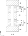
- FIGS. 2 A and 2 B are diagrams illustrating a structure of a semiconductor device according to an embodiment of the present disclosure.
- FIG. 2 A may be a cross-sectional view along the line A-A′ in the first direction I of FIG. 1
- FIG. 2 B may be a cross-sectional view along the line B-B′ in the second direction II of FIG. 1 .
- a content repetitive to the previously described content may be omitted for the interest of brevity.
- the semiconductor device may include the first deck D 1 and the second deck D 2 .
- the first deck D 1 may include a plurality of first row lines 10 , a plurality of first memory cells MC 1 , and a plurality of column lines 30 .
- the second deck D 2 may include a plurality of second row lines 20 , a plurality of second memory cells MC 2 , and the plurality of column lines 30 .
- Each of the first memory cells MC 1 may include a first electrode 11 , a second electrode 12 , a first variable resistance layer 13 , and a first resistance element (e.g., a first dielectric layer 14 ).
- the first electrode 11 may be a portion of the first row line 10 or may be electrically connected to the first row line 10 .
- the first electrode 11 may include a conductive material such as polysilicon or metal.
- the first electrodes 11 may include polysilicon, tungsten (W), tungsten nitride (WNx), tungsten silicide (WSix), titanium (Ti), titanium nitride (TiNx), titanium silicon nitride (TiSiN), titanium aluminum nitride (TiAlN), tantalum (Ta), tantalum nitride (TaN), tantalum silicon nitride (TaSiN), tantalum aluminum nitride (TaAIN), carbon (C), silicon carbide (SiC), silicon carbon nitride (SiCN), copper (Cu), zinc (Zn), nickel (Ni), cobalt (Co), lead (Pd), platinum (Pt), molybdenum (Mo), ruthenium (Ru), or the like, or may include a combination thereof.
- the second electrode 12 may be a portion of the column line 30 or may be electrically connected to the column line 30 . As an embodiment, when the first electrode 11 is electrically connected to the word line, the second electrode 12 may be electrically connected to the bit line.
- the second electrodes 12 may include the same material as the first electrodes 11 or may include a material different from that of the first electrodes 11 .
- the second electrodes 12 may include a conductive material such as polysilicon or metal.
- the second electrodes 12 may include polysilicon, tungsten (W), tungsten nitride (WNx), tungsten silicide (WSix), titanium (Ti), titanium nitride (TiNx), titanium silicon nitride (TiSiN), titanium aluminum nitride (TiAlN), tantalum (Ta), tantalum nitride (TaN), tantalum silicon nitride (TaSiN), tantalum aluminum nitride (TaAIN), carbon (C), silicon carbide (SiC), silicon carbon nitride (SiCN), copper (Cu), zinc (Zn), nickel (Ni), cobalt (Co), lead (Pd), platinum (Pt), molybdenum (Mo), ruthenium (Ru), or the like, or may include a combination thereof.
- the first variable resistance layer 13 may be positioned between the first electrode 11 and the second electrode 12 .
- the first variable resistance layer 13 may include a resistive material, and may have a property of reversibly transitioning between different resistance states according to an applied voltage or current.
- the first variable resistive layer 13 may be used as a data storage and a selection element simultaneously.
- the first variable resistance layer 13 may include a variable resistance material of which a resistance changes without a phase change, and may include a chalcogenide-based material.
- the first variable resistive layer 13 may include germanium (Ge), antimony (Sb), tellurium (Te), arsenic (As), selenium (Se), silicon (Si), indium (In), tin (Sn), sulfur (S), gallium (Ga), or the like, or may include a combination thereof.
- the first variable resistance layer 13 may further include boron (B), nitrogen (N), carbon (C), bismuth (Bi), nickel (Ni), manganese (Mn), silver (Ag), or the like, or may further include a combination thereof.
- the first variable resistance layer 13 may maintain an amorphous state during the program operation, and may not be changed to a crystalline state after the program operation.
- a threshold voltage of the first memory cell MC 1 may be changed according to a program voltage applied to the first memory cell MC 1 . According to the threshold voltage, the first memory cell MC 1 may be programmed to at least two states.
- the first dielectric layer 14 may be positioned between the first variable resistance layer 13 and the first row line 10 . As an embodiment, the first dielectric layer 14 may be positioned between the first variable resistance layer 13 and the first electrode 11 . The first dielectric layer 14 may be in contact with the first electrode 11 and the first variable resistance layer 13 . When performing the program operation, a current may flow through the first dielectric layer 14 , and thus data may be stored in the first memory cell MC 1 .
- the first dielectric layer 14 may have a thickness of 1 to 20 ⁇ . In an embodiment, the first dielectric layer 14 may have a thickness of 5 to 10 ⁇ or 8 to 13 ⁇ .
- the first dielectric layer 14 may include a dielectric material such as oxide or nitride.
- the first dielectric layer 14 may include silicon oxide (SiOx), silicon nitride (SiNx), aluminum oxide (AlOx), zirconium oxide (ZrO 2 ), hafnium oxide (HfOx), titanium oxide (TiOx), or tantalum oxide (TaOx), or may include a combination thereof.
- the first memory cell MC 1 may have an asymmetric structure by the first dielectric layer 14 .
- the first memory cell MC 1 may have an asymmetric structure by including the first dielectric layer 14 such that the first memory cell MC 1 has a first interface between the first electrode 11 and the first dielectric layer 14 and a second interface between the second electrode 12 and the first variable resistance layer 13 , the first interface having the higher resistivity than the second interface.
- the first dielectric layer 14 may be positioned only between the first row line 10 and the first variable resistance layer 13 , and the first dielectric layer 14 may not be positioned between the column line 30 and the first variable resistance layer 13 .
- the first dielectric layer 14 may act as a barrier layer.
- the second memory cells MC 2 may have a configuration similar to that of the first memory cells MC 1 .
- Each of the second memory cells MC 2 may include a first electrode 21 , a second electrode 22 , a second variable resistance layer 23 , and a second resistance element (e.g., a second dielectric layer 24 ).
- the first electrode 21 may be a portion of the second row line 20 or may be electrically connected to the second row line 20 .
- the first electrode 21 may include the same material as the first electrode 11 of the first memory cell MC 1 or may include a material different from that of the first electrode 11 of the first memory cell MC 1 .
- the second electrode 22 may be a portion of the column line 30 or may be electrically connected to the column line 30 .
- the second electrode 22 may include the same material as the second electrode 12 of the first memory cell MC 1 or may include a material different from that of the second electrode 12 of the first memory cell MC 1 .
- the second variable resistance layer 23 may be positioned between the first electrode 21 and the second electrode 22 .
- the second variable resistance layer 23 may include the same material as the first variable resistance layer 13 or may include a material different from that of the first variable resistance layer 13 .
- the second variable resistance layer 23 may include a resistive material, and may have a property of reversibly transitioning between different resistance states according to an applied voltage or current.
- the second variable resistive layer 23 may be used as a data storage and a selection element simultaneously.
- the second dielectric layer 24 may be positioned between the second variable resistance layer 23 and the second row line 20 . As an embodiment, the second dielectric layer 24 may be positioned between the second variable resistance layer 23 and the first electrode 21 . The second dielectric layer 24 may be in contact with the first electrode 21 and the second variable resistance layer 23 . When performing the program operation, a current may flow through the second dielectric layer 24 , and thus data may be stored in the second memory cell MC 2 .
- the second dielectric layer 24 may have a thickness of 1 to 20 ⁇ .
- the second dielectric layer 24 may include the same material as the first dielectric layer 14 or may include a material different from that of the first dielectric layer 14 .
- the second dielectric layer 24 may include a dielectric material such as oxide or nitride.
- the second dielectric layer 24 may include silicon oxide (SiOx), silicon nitride (SiNx), aluminum oxide (AlOx), zirconium oxide (ZrO 2 ), hafnium oxide (HfOx), titanium oxide (TiOx), or tantalum oxide. (TaOx), or may include a combination thereof.
- the second memory cell MC 2 may have an asymmetric structure by the second dielectric layer 24 .
- the second dielectric layer 24 may be positioned only between the second row line 20 and the second variable resistance layer 23 , and the second dielectric layer 24 may not be positioned between the column line 30 and the second variable resistance layer 23 .
- the first memory cell MC 1 and the second memory cell MC 2 may have a symmetric structure.
- the second dielectric layer 24 may act as a barrier layer.
- each of the first memory cells MC 1 and the second memory cells MC 2 may have an asymmetric structure. Through this, a change width of the threshold voltage may be increased, and a read window margin may be secured.
- a first threshold voltage may result when a first program pulse having a first polarity and a read pulse having the first polarity are applied across the first memory cell MC 1 .
- a second threshold voltage higher than the first threshold voltage may result when a second program pulse having a second polarity and a read pulse having the first polarity are applied across the first memory cell MC 1 .
- the first memory cell MC 1 When the column line 30 functions as a bit line and the first row line 10 functions as a word line, the first memory cell MC 1 has an asymmetric structure in which the first dielectric layer 14 is disposed closer to the first row line 10 than the column line 30 , thereby increasing the second threshold voltage compared to when the first memory cell MC 1 does not include the first dielectric layer 14 . Since a read window margin of the first memory cell MC 1 is a difference between the second threshold voltage and the first threshold voltage, the asymmetric structure of the first memory cell MC 1 may increase the read window margin to improve the reliability of the first memory cell MC 1 .
- the second memory cell MC 2 has an asymmetric structure in which the second dielectric layer 24 is disposed closer to the second row line 20 than the column line 30 , thereby increasing a read window margin of the second memory cell MC 2 to improve the reliability of the second memory cell MC 2 .
- the first memory cells MC 1 and the second memory cells MC 2 may have a symmetric structure based on the column line 30 .
- the second electrode 12 , the first variable resistance layer 13 , the first dielectric layer 14 , and the first electrode 11 of the first memory cell MC 1 may correspond to the second electrode 22 , the second variable resistance layer 23 , the second dielectric layer 24 , and the first electrode 21 of the second memory cell MC 2 , respectively, with respect to the column line 30 .
- both of the first deck D 1 and the second deck D 2 may increase the threshold voltage change width.
- the first memory cells MC 1 may include the first dielectric layers 14 and the second memory cells MC 2 may not include the second dielectric layers 24 .
- the first memory cells MC 1 may not include the first dielectric layers 14 and the second memory cells MC 2 may include the second dielectric layers 24 .
- FIGS. 3 A and 3 B are diagrams illustrating a structure of a semiconductor device according to an embodiment of the present disclosure.
- FIG. 3 A may be a cross-sectional view along the line AA′ in the first direction I of FIG. 1
- FIG. 3 B may be a cross-sectional view along the line BB′ in the second direction II of FIG. 1 .
- a content repetitive to the previously described content may be omitted for the interest of brevity.
- the semiconductor device may include a first deck D 1 and a second deck D 2 .
- the first deck D 1 may include a plurality of first row lines 10 , a plurality of first memory cells MC 1 , and a plurality of column lines 30 .
- the second deck D 2 may include a plurality of second row lines 20 , a plurality of second memory cells MC 2 , and the plurality of column lines 30 .
- Each of the first memory cells MC 1 may include a first electrode 11 ′, a second electrode 12 , and a first variable resistance layer 13 .
- the first electrode 11 ′ may include a first portion 11 _P 1 adjacent to the first row line 10 and a second portion 11 _P 2 adjacent to the first variable resistance layer 13 .
- the second portion 11 _P 2 may have a specific resistance higher than that of the first portion 11 _P 1 .
- the second portion 11 _P 2 may have a nitrogen concentration higher than that of the first portion 11 _P 1 .
- the first portion 11 _P 1 and the second portion 11 _P 2 may be films formed by a separate deposition process, and an interface may exist between the first portion 11 _P 1 and the second portion 11 _P 2 .
- the second portion 11 _P 2 may be formed by performing a surface treatment on the first electrode 11 , and an interface may not exist between the first portion 11 _P 1 and the second portion 11 _P 2 .
- the first memory cell MC 1 may have an asymmetric structure by the second portion 11 _P 2 .
- the second electrode 12 may not include a portion having a relatively high specific resistance.
- the first electrode 11 ′ may have a specific resistance higher than that of the second electrode 12 .
- the second portion 11 _P 2 may have a specific resistance higher than that of the second electrode 12 or may have a nitrogen concentration higher than that of the second electrode 12 .
- the first portion 11 _P 1 and the second portion 11 _P 2 may have a specific resistance higher than that of the second electrode 12 or may have a nitrogen concentration higher than that of the second electrode 12 .
- the second memory cells MC 2 may have a configuration similar to that of the first memory cells MC 1 .
- Each of the second memory cells MC 2 may include a first electrode 21 ′, a second electrode 22 , and a second variable resistance layer 23 .
- the first electrode 21 ′ may include a first portion 21 _P 1 adjacent to the second row line 20 and a second portion 21 _P 2 adjacent to the second variable resistance layer 23 .
- the second portion 21 _P 2 may have a specific resistance higher than that of the first portion 21 _P 1 .
- the second portion 21 _P 2 may have a nitrogen concentration higher than that of the first portion 21 _P 1 .
- the second memory cell MC 2 may have an asymmetric structure by the second portion 21 _P 2 .
- the second electrode 22 may not include a portion having a relatively high specific resistance.
- the first electrode 21 ′ may have a specific resistance higher than that of the second electrode 22 .
- the second portion 21 _P 2 may have a specific resistance higher than that of the second electrode 22 or may have a nitrogen concentration higher than that of the second electrode 22 .
- the first portion 21 _P 1 and the second portion 21 _P 2 may have a specific resistance higher than that of the second electrode 22 or may have a nitrogen concentration higher than that of the second electrode 22 .
- each of the first memory cells MC 1 and the second memory cells MC 2 may have an asymmetric structure. Through this, the change width of the threshold voltage may be increased, and the read window margin may be secured.
- the first memory cells MC 1 and the second memory cells MC 2 may have a symmetric structure based on the column line 30 . Through this, both of the first deck D 1 and the second deck D 2 may increase the threshold voltage change width.
- the first memory cells MC 1 may include the second portion 11 _P 2 and the second memory cells MC 2 may not include the second portion 21 _P 2 .
- the first memory cells MC 1 may not include the second portion 11 _P 2 and the second memory cells MC 2 may include the second portion 21 _P 2 .
- FIGS. 4 A and 4 B are diagrams illustrating an operation of a semiconductor device according to an embodiment of the present disclosure.
- an x-axis may indicate a time and a y-axis may indicate a voltage.
- a content repetitive to the previously described content may be omitted for the interest of brevity.
- FIG. 4 A illustrates performing a first operation (e.g., a set operation) on one or more of the plurality of first memory cells MC 1 included in the first deck D 1 .
- a program pulse P PGM of a first polarity is applied to a first memory cell MC 1 selected from among the plurality of first memory cells MC 1 .
- the first polarity may be a positive polarity.
- a first voltage e.g., a positive voltage
- a second voltage e.g., 0V
- a read pulse P READ of the first polarity may be applied to a first memory cell MC 1 selected from among the plurality of first memory cells MC 1 .
- FIG. 4 B illustrates performing a second operation (e.g., a reset operation) on one or more of the plurality of first memory cells MC 1 included in the second deck D 2 .
- a program pulse P PGM of a second polarity different from the first polarity is applied to a first memory cell MC 1 selected from among the plurality of first memory cells MC 1 .
- the second polarity may be a negative polarity.
- a first voltage e.g., 0V
- a second voltage e.g., a positive voltage
- a read pulse P READ of the first polarity may be applied to a first memory cell MC 1 selected from among the plurality of first memory cells MC 1 .
- the first polarity may be the positive polarity.
- the program pulse P PGM of the second polarity used during the reset operation and the program pulse P PGM of the first polarity used during the set operation may have substantially the same waveform except that the polarities are different.
- the waveform may include a pulse width, a peak value, and the like.
- the first memory cell MC 1 of a set state may have a first threshold voltage.
- the first memory cell MC 1 of the reset state may have a second threshold voltage different from the first threshold voltage.
- the second threshold voltage may have a level higher than that of the first threshold voltage.
- the first memory cell MC 1 may have the first threshold voltage when the program pulse P PGM and the read pulse P READ have the same polarity (e.g., the first polarity), whereas the first memory cell MC 1 may have the second threshold voltage higher than the first threshold voltage when the program pulse P PGM and the read pulse P READ have opposite polarities. Therefore, data may be stored in the first memory cell MC 1 by using a threshold voltage difference.
- the first memory cells MC 1 may have the second threshold voltage higher than that of a memory cell that does not include the first dielectric layer 14 or the second portion 11 _P 2 or a memory cell having a symmetric structure.
- the program pulse P PGM of a second polarity is applied to the first memory cell MC 1 during the reset operation and the read pulse P READ of a first polarity is applied to the first memory cell MC 1 by applying a first voltage to a first line (e.g., the first row line 10 ) and a second voltage to a second line (e.g., the column line 30 ), the second voltage being higher than the first voltage, the first dielectric layer 14 or the second portion 11 _P 2 of the first memory cell MC 1 may be disposed closer to the first line than the second line. Therefore, the change width of the threshold voltage may be increased, and the read window margin may be secured.
- a first line e.g., the first row line 10
- a second voltage e.g., the column line 30
- FIGS. 5 A and 5 B are diagrams illustrating an operation of a semiconductor device according to an embodiment of the present disclosure.
- an x-axis may indicate a time and a y-axis may indicate a voltage.
- FIG. 5 A illustrates performing a first operation (e.g., a set operation) on one or more of the plurality of second memory cells MC 2 included in the second deck D 2 .
- a program pulse P PGM of a second polarity is applied to a second memory cell MC 2 selected from among the plurality of second memory cells MC 2 .
- the second polarity may be a negative polarity.
- a first voltage e.g., 0V
- a second voltage e.g., a positive voltage
- a read pulse P READ of the second polarity may be applied to a second memory cell MC 2 selected from among the plurality of second memory cells MC 2 .
- FIG. 5 B illustrates performing a second operation (e.g., a reset operation) on one or more of the plurality of second memory cells MC 2 included in the second deck D 2 .
- a program pulse P PGM of a first polarity is applied to a second memory cell MC 2 selected from among the plurality of second memory cells MC 2 .
- the first polarity may be a positive polarity.
- a first voltage e.g., a positive voltage
- a second voltage e.g., 0V
- a read pulse P READ of the second polarity may be applied to a second memory cell MC 2 selected from among the plurality of second memory cells MC 2 .
- the second polarity may be the negative polarity.
- the program pulse P PGM of the first polarity used during the reset operation and the program pulse P PGM of the second polarity used during the set operation may have substantially the same waveform except that the polarities are different. Alternatively, not only the polarity but also the waveform may be different.
- the second memory cell MC 2 of a set state may have a first threshold voltage.
- the second memory cell MC 2 of the reset state may have a second threshold voltage higher than the first threshold voltage. Therefore, data may be stored in the second memory cell MC 2 by using a threshold voltage difference.
- the second memory cells MC 2 not only have an asymmetric structure by the second dielectric layer 24 or the second portion 21 _P 2 , but also have a symmetric structure with the first memory cells MC 1 based on the column line 30 . Even though the second memory cells MC 2 have the asymmetric structure, when the second dielectric layer 24 or the second portion 21 _P 2 is positioned between the column line 30 and the second variable resistance layer 23 , the second threshold voltage may decrease.
- the read pulse P READ of a second polarity may be applied to the second memory cell MC 2 by applying a first voltage to a first line (e.g., the column line 30 ) and a second voltage to a second line (e.g., the second row line 20 ), the first voltage being higher than the second voltage.
- a first line e.g., the column line 30
- a second voltage e.g., the second row line 20
- the second dielectric layer 24 or the second portion 21 _P 2 of the second memory cell MC 2 may be positioned between the column line 30 and the second variable resistance layer 23 to dispose the second dielectric layer 24 or the second portion 21 _P 2 farther from the second row line 20 than from the column line 30 , the second threshold voltage may decrease and thus the read window margin may also decrease.
- the second dielectric layer 24 or the second portion 21 _P 2 may be positioned between the second row line 20 and the second variable resistance layer 23 to dispose the second dielectric layer 24 or the second portion 21 _P 2 closer to the second row line 20 than to the column line 30 .
- the second threshold voltage of the second memory cells MC 2 may increase and thus the read window margin may also increase. Namely, the change width of the threshold voltage may be increased, and the read window margin may be secured.
- the program pulse of the first polarity may be used during the set operation of the first memory cells MC 1
- the program pulse of the second polarity may be used during the set operation of the second memory cells MC 2
- the second program pulse of the second polarity may be used during the reset operation of the first memory cells MC 1
- the first program pulse of the first polarity may be used during the set operation of the second memory cells MC 2 .
- the program pulse P PGM used during the set operation of the first memory cells MC 1 and the program pulse P PGM used during the reset operation of the second memory cells MC 2 may have the same polarity and substantially the same waveform. Alternatively, only the polarity may be the same and the waveform may be different.
- the program pulse P PGM used during the reset operation of the first memory cells MC 1 and the program pulse P PGM used during the set operation of the second memory cells MC 2 may have the same polarity and substantially the same waveform. Alternatively, only the polarity may be the same and the waveform may be different.
- the read pulse P READ of the first polarity may be used during the read operation of the first memory cells MC 1
- the read pulse P READ of the second polarity may be used during the read operation of the second memory cells MC 2 .
- the read pulse P READ of the first polarity and the read pulse P READ of the second polarity may have substantially the same waveform except that the polarities are different. Alternatively, not only the polarity but also the waveform may be different.
- the first memory cells MC 1 of the first deck D 1 and the second memory cells MC 2 of the second deck D 2 may be programmed using the program pulse V PGM of different polarities.
- the first memory cells MC 1 of the first deck D 1 and the second memory cells MC 2 of the second deck D 2 may be read using the read pulse V READ of different polarities. Therefore, read margins of both of the first memory cells MC 1 and the second memory cells MC 2 may be secured.
- FIGS. 6 to 9 illustrate some examples of a device or a system that may implement the memory circuit or the semiconductor device of the above-described embodiments.
- FIG. 6 is an example of a configuration diagram of a microprocessor implementing a memory device according to an embodiment of the present disclosure.
- the microprocessor 1000 may control and adjust a series of processes of receiving data from various external devices, processing the data, and transmitting a result of the process to the external device, and may include a memory 1010 , an operating component 1020 , a controller 1030 , and the like.
- the microprocessor 1000 may be various data processing devices such as a central processing unit (CPU), a graphic processing unit (GPU), and a digital signal processor (DSP), an application processor.
- CPU central processing unit
- GPU graphic processing unit
- DSP digital signal processor
- the memory 1010 may be a processor register, a register, or the like, may store data in the microprocessor 1000 , may include various registers such as a data register, an address register, and a floating point register.
- the memory 1010 may temporarily store addresses at which data for performing an operation in the operating component 1020 , data of a result of the performance, and data for the performance are stored.
- the memory 1010 may include one or more embodiments of the semiconductor device described above.
- the memory 1010 may include one or more memory elements.
- the memory element may include first row lines extending in a first direction, column lines extending in a second direction crossing the first direction, second row lines extending in the first direction, first memory cells respectively connected between the first row lines and the column lines and including a first variable resistance layer and a first dielectric layer positioned between the first variable resistance layer and the first row line, and second memory cells respectively connected between the second row lines and the column lines and including a second variable resistance layer and a second dielectric layer positioned between the second variable resistance layer and the second row line. Therefore, reliability of the memory 1010 may be improved and a manufacturing process may be improved. As a result, an operation characteristic of the microprocessor 1000 may be improved.
- the operating component 1020 may perform various arithmetic operations or logical operations according to a result obtained by decoding an instruction by the controller 1030 .
- the operating component 1020 may include one or more arithmetic and logic units (ALUs) and the like.
- the controller 1030 may receive a signal from an external device such as the memory 1010 , the operating component 1020 , and the microprocessor 1000 , perform extraction or decoding of an instruction and control of a signal input/output of the microprocessor 1000 , and the like, and execute a process indicated by a program.
- the microprocessor 1000 may further include a cache memory 1040 capable of temporarily storing data input from an external device or data to be output to an external device, in addition to the memory 1010 .
- the cache memory 1040 may exchange data with the memory 1010 , the operating component 1020 , and the controller 1030 through a bus interface 1050 .
- FIG. 7 is an example of a configuration diagram of a processor implementing a memory device according to an embodiment of the present disclosure.
- the processor 1100 may include various functions in addition to the functions of the microprocessor 1000 described above, and thus performance may be improved and multi-function may be implemented.
- the processor 1100 may include a core 1110 serving as a microprocessor, a cache memory 1120 temporarily store data, and a bus interface 1130 for transferring data between internal and external devices.
- the processor 1100 may include various system on chips (SoCs) such as a multi core processor, a graphic processing unit (GPU), and an application processor (AP).
- SoCs system on chips
- the core 1110 of the present embodiment may be a part for performing an arithmetic logic operation on data input from an external device and may include a memory 1111 , an operating component 1112 , and a controller 1113 .
- the memory 1111 , the operating component 1112 , and the controller 1113 may be substantially the same as the memory 1010 , the operating component 1020 , and the controller 1030 described above.
- the cache memory 1120 temporarily stores data to compensate for a data process speed difference between the core 1110 operating at a high speed and an external device operating at a low speed.
- the cache memory 1120 may include a primary storage 1121 and a secondary storage 1122 , and may include a tertiary storage 1123 when a high capacity is required.
- the cache memory 1120 may include more storages as needed. That is, the number of storages included in the cache memory 1120 may vary depending on design.
- process speeds for storing and discriminating data in the primary, secondary, and tertiary storages 1121 , 1122 , and 1123 may be the same or different. When the process speeds of each storage are different, the speed of the primary storage may be the fastest.
- the primary storage 1121 , the secondary storage 1122 , and the tertiary storage 1123 of the cache memory 1120 may include one or more embodiments of the semiconductor device described above.
- the cache memory 1120 may include one or more memory elements.
- the memory element may include first row lines extending in a first direction, column lines extending in a second direction crossing the first direction, second row lines extending in the first direction, first memory cells respectively connected between the first row lines and the column lines and including a first variable resistance layer and a first dielectric layer positioned between the first variable resistance layer and the first row line, and second memory cells respectively connected between the second row lines and the column lines and including a second variable resistance layer and a second dielectric layer positioned between the second variable resistance layer and the second row line. Therefore, reliability of the cache memory 1120 may be improved and a manufacturing process may be improved. As a result, an operation characteristic of the processor 1100 may be improved.
- the primary, secondary, and tertiary storages 1121 , 1122 , and 1123 are configured in the cache memory 1120 .
- some or all of the primary, secondary, and tertiary storages 1121 , 1122 , and 1123 may be configured inside the core 1110 and compensate for the process speed difference between the core 1110 and the external device.
- the bus interface 1130 connects the core 1110 , the cache memory 1120 , and an external device so as to efficiently transmit data.
- the processor 1100 may include a plurality of cores 1110 and the plurality of cores 1110 may share the cache memory 1120 .
- the plurality of cores 1110 and the cache memory 1120 may be directly connected to each other or may be connected to each other through the bus interface 1130 . All of the plurality of cores 1110 may be configured identically to the core described above.
- the processor 1100 may include an embedded memory 1140 that stores data, a communication module 1150 that may transmit and receive data in a wired manner or wirelessly with an external device, a memory controller 1160 that drives an external storage device, a media processor 1170 that processes data processed by the processor 1100 and input from an external input device and outputs the processed data to an external interface device, and the like.
- the processor 1100 may further include a plurality of modules and devices. In this case, the plurality of added modules may exchange data with the core 1110 and the cache memory 1120 through the bus interface 1130 .
- the embedded memory 1140 may include a non-volatile memory as well as a volatile memory.
- the volatile memory may include a dynamic random access memory (DRAM), a mobile DRAM, a static random access memory (SRAM), a memory performing a function similar to that of these, and the like.
- the non-volatile memory may include a read only memory (ROM), a NOR flash memory, a NAND flash memory, a phase change random access memory (PRAM), a resistive random access memory (RRAM), a spin transfer torque random access memory (STTRAM), a magnetic random access memory (MRAM), a memory performing a function similar to that of these, and the like.
- the communication module 1150 may include a module capable of connecting with a wired network, a module capable of connecting with a wireless network, and both of the modules capable of connecting with a wired network and the module capable of connecting with a wireless network.
- a wired network module may include a local area network (LAN), a universal serial bus (USB), an Ethernet, a power line communication (PLC), or the like, as various devices that transmit and receive data through a transmission line.
- a wireless network module may include an infrared data association (IrDA), a code division multiple access (CDMA), a time division multiple access (TDMA), a frequency division multiple access (FDMA), a wireless LAN, Zigbee, a ubiquitous sensor network (USN), Bluetooth, radio frequency identification (RFID), long term evolution (LTE), near field communication (NFC), wireless broadband Internet (WIBRO), high speed downlink packet access (HSDPA), wideband CDMA (WCDMA), ultra wide band (UWB), and the like, as various devices that transmit and receive data without a transmission line.
- IrDA infrared data association
- CDMA code division multiple access
- TDMA time division multiple access
- FDMA frequency division multiple access
- WLAN Zigbee
- USB ubiquitous sensor network
- RFID radio frequency identification
- LTE long term evolution
- NFC near field communication
- WIBRO wireless broadband Internet
- HSDPA high speed downlink packet access
- WCDMA wideband CDMA
- UWB ultra wide band
- the memory controller 1160 is for processing and managing data transmitted between the processor 1100 and an external storage device operating according to a different communication standard.
- the memory controller 1160 may include various memory controllers, for example, a controller that controls integrated device electronics (IDE), serial advanced technology attachment (SATA), a small computer system interface (SCSI), redundant array of independent disks (RAID), a solid state drive (SSD), external SATA (eSATA), personal computer memory card international association (PCMCIA), a universal serial bus (USB), a secure digital (SD) card, a mini secure digital (mSD) card, a micro secure digital (micro SD) card, a secure digital high capacity (SDHC) card, a memory stick card, a smart media (SM) card, a multi-media card (MMC), an embedded MMC (eMMC), a compact flash (CF) card, and the like.
- IDE integrated device electronics
- SATA serial advanced technology attachment
- SCSI small computer system interface
- RAID redundant array of independent disks
- SSD solid state drive
- the media processor 1170 may process data processed by the processor 1100 and data input as an image, a voice, and other formats from an external input device, and may output the data to an external interface device.
- the media processor 1170 may include a graphics processing unit (GPU), a digital signal processor (DSP), high-definition audio (HD Audio), high-definition multimedia interface (HDMI) controller, and the like.
- FIG. 8 is an example of a configuration diagram of a system implementing a memory device according to an embodiment of the present disclosure.
- the system 1200 is a device that processes data, and may perform input, process, output, communication, storage, and the like in order to perform a series of operations on data.
- the system 1200 may include a processor 1210 , a main memory device 1220 , an auxiliary memory device 1230 , an interface device 1240 , and the like.
- the system 1200 of the present embodiment may be various electronic systems operating using a processor, such as a computer, a server, a personal digital assistant (PDA), a portable computer, a web tablet, a wireless phone, a mobile phone, a smart phone, a digital music player, a portable multimedia player (PMP), a camera, a global positioning system (GPS), a video camera, a voice recorder, telematics, an audio visual system, a smart television, or the like.
- a processor such as a computer, a server, a personal digital assistant (PDA), a portable computer, a web tablet, a wireless phone, a mobile phone, a smart phone, a digital music player, a portable multimedia player (PMP), a camera, a global positioning system (GPS), a video camera, a voice recorder, telematics, an audio visual system, a smart television, or the like.
- PDA personal digital assistant
- PMP portable multimedia player
- GPS global positioning system
- video camera a
- the processor 1210 may control processes of analysis of an input command, an operation, comparison, and the like of data stored in the system 1200 , and may be substantially the same as the microprocessor 1000 or processor 1100 described above.
- the main memory device 1220 may be a memory space capable of moving, storing, and executing a program code or data from the auxiliary memory device 1230 when the program is executed. A stored content may be preserved even though power is shut off.
- the auxiliary memory device 1230 refers to a memory device for storing a program code or data.
- the auxiliary memory device 1230 is slower than the main memory device 1220 but may store a lot of data.
- the main memory device 1220 or the auxiliary memory device 1230 may include one or more embodiments of the electronic device described above.
- the main memory device 1220 or the auxiliary memory device 1230 may include one or more memory elements.
- the memory element may include first row lines extending in a first direction, column lines extending in a second direction crossing the first direction, second row lines extending in the first direction, first memory cells respectively connected between the first row lines and the column lines and including a first variable resistance layer and a first dielectric layer positioned between the first variable resistance layer and the first row line, and second memory cells respectively connected between the second row lines and the column lines and including a second variable resistance layer and a second dielectric layer positioned between the second variable resistance layer and the second row line. Therefore, reliability of the main memory device 1220 or the auxiliary memory device 1230 may be improved and a manufacturing process may be improved. As a result, an operation characteristic of the system 1200 may be improved.
- main memory device 1220 or the auxiliary memory device 1230 may include a memory system 1300 as shown in FIG. 9 in addition to the semiconductor device of the above-described embodiment or without the semiconductor device of the above-described embodiment.
- the interface device 1240 may be for exchanging an instruction, data, and the like between the system 1200 of the present embodiment and an external device.
- the interface device 1240 may be a keypad, a keyboard, a mouse, a speaker, a microphone, a display, various human interface devices (HIDs), a communication device, and the like.
- the communication device may be substantially the same as the communication module 1150 described above.
- FIG. 9 is an example of a configuration diagram of a memory system implementing a memory device according to an embodiment of the present disclosure.
- the memory system 1300 may include a memory 1310 having a nonvolatile characteristic as a configuration for storing data, a controller 1320 for controlling the memory 1310 , an interface 1330 for connection with an external device, and a buffer memory 1340 for temporarily storing data in order to efficiently transfer input/output of data between the interface 1330 and the memory 1310 .
- the memory system 1300 may mean a memory for simply storing data, and further, may mean a data storage device that conserves stored data for a long time.
- the memory system 1300 may be a disk type such as a solid state drive (SSD), and a card type such as a universal serial bus (USB) memory, a secure digital (SD) card, a mini secure digital (mSD) card, a micro secure digital (micro SD) card, a secure digital high capacity (SDHC) card, a memory stick card, a smart media (SM) card, a multi-media card (MMC), an embedded MMC (eMMC), and a compact flash (CF) card.
- SSD solid state drive
- a card type such as a universal serial bus (USB) memory, a secure digital (SD) card, a mini secure digital (mSD) card, a micro secure digital (micro SD) card, a secure digital high capacity (SDHC) card, a memory stick card, a smart media (SM) card, a multi-media card (MMC), an embedded MMC (eMMC), and a compact flash (CF) card.
- SSD solid state drive
- CF compact flash
- the memory 1310 or the buffer memory 1340 may include one or more embodiments of the semiconductor device described above.
- the memory 1310 or the buffer memory 1340 may include one or more memory elements.
- the memory element may include first row lines extending in a first direction, column lines extending in a second direction crossing the first direction, second row lines extending in the first direction, first memory cells respectively connected between the first row lines and the column lines and including a first variable resistance layer and a first dielectric layer positioned between the first variable resistance layer and the first row line, and second memory cells respectively connected between the second row lines and the column lines and including a second variable resistance layer and a second dielectric layer positioned between the second variable resistance layer and the second row line. Therefore, reliability of the memory 1310 or the buffer memory 1340 may be improved and a manufacturing process may be improved. As a result, an operation characteristic of the memory system 1300 may be improved.
- the memory 1310 or the buffer memory 1340 may include various volatile or nonvolatile memories in addition to the semiconductor device of the above-described embodiment or without the semiconductor device of the above-described embodiment.
- the controller 1320 may control exchange of data between the memory 1310 and the interface 1330 .
- the controller 1320 may include a processor 1321 that performs an operation or the like for processing commands input through the interface 1330 from the outside of the memory system 1300 .
- the interface 1330 is for exchanging an instruction, data, and the like between the memory system 1300 and an external device.
- the interface 1330 may be compatible with interfaces used in such a card type or disk type device, or may be compatible with interfaces used in a device similar to the card type or disk type device.
- the interface 1330 may be compatible with one or more interfaces having different types.
- an operation characteristic and reliability of a memory cell may be improved.
Abstract
Description
Claims (16)
Applications Claiming Priority (2)
| Application Number | Priority Date | Filing Date | Title |
|---|---|---|---|
| KR1020210046126A KR20220139747A (en) | 2021-04-08 | 2021-04-08 | Semiconductor device |
| KR10-2021-0046126 | 2021-04-08 |
Publications (2)
| Publication Number | Publication Date |
|---|---|
| US20220328563A1 US20220328563A1 (en) | 2022-10-13 |
| US11864394B2 true US11864394B2 (en) | 2024-01-02 |
Family
ID=83509561
Family Applications (1)
| Application Number | Title | Priority Date | Filing Date |
|---|---|---|---|
| US17/494,534 Active 2042-04-08 US11864394B2 (en) | 2021-04-08 | 2021-10-05 | Semiconductor device |
Country Status (3)
| Country | Link |
|---|---|
| US (1) | US11864394B2 (en) |
| KR (1) | KR20220139747A (en) |
| CN (1) | CN115207025A (en) |
Citations (7)
| Publication number | Priority date | Publication date | Assignee | Title |
|---|---|---|---|---|
| US20110210303A1 (en) * | 2008-09-02 | 2011-09-01 | Kabushiki Kaisha Toshiba | Nonvolatile semiconductor memory device |
| US9287498B2 (en) | 2011-09-14 | 2016-03-15 | Intel Corporation | Dielectric thin film on electrodes for resistance change memory devices |
| US10157667B2 (en) | 2017-04-28 | 2018-12-18 | Micron Technology, Inc. | Mixed cross point memory |
| US10193064B2 (en) | 2014-09-03 | 2019-01-29 | Micron Technology, Inc. | Memory cells including dielectric materials, memory devices including the memory cells, and methods of forming same |
| US20190067571A1 (en) * | 2017-08-25 | 2019-02-28 | Micron Technology, Inc. | Self-selecting memory cell with dielectric barrier |
| US20190311760A1 (en) * | 2010-02-15 | 2019-10-10 | Micron Technology, Inc. | Cross-Point Memory Cells, Non-Volatile Memory Arrays, Methods of Reading a Memory Cell, Methods of Programming a Memory Cell, Methods of Writing to and Reading from a Memory Cell, and Computer Systems |
| US20210064455A1 (en) * | 2019-08-28 | 2021-03-04 | Micron Technology, Inc. | Error correction for content-addressable memory |
-
2021
- 2021-04-08 KR KR1020210046126A patent/KR20220139747A/en active Search and Examination
- 2021-10-05 US US17/494,534 patent/US11864394B2/en active Active
-
2022
- 2022-03-01 CN CN202210193307.2A patent/CN115207025A/en active Pending
Patent Citations (7)
| Publication number | Priority date | Publication date | Assignee | Title |
|---|---|---|---|---|
| US20110210303A1 (en) * | 2008-09-02 | 2011-09-01 | Kabushiki Kaisha Toshiba | Nonvolatile semiconductor memory device |
| US20190311760A1 (en) * | 2010-02-15 | 2019-10-10 | Micron Technology, Inc. | Cross-Point Memory Cells, Non-Volatile Memory Arrays, Methods of Reading a Memory Cell, Methods of Programming a Memory Cell, Methods of Writing to and Reading from a Memory Cell, and Computer Systems |
| US9287498B2 (en) | 2011-09-14 | 2016-03-15 | Intel Corporation | Dielectric thin film on electrodes for resistance change memory devices |
| US10193064B2 (en) | 2014-09-03 | 2019-01-29 | Micron Technology, Inc. | Memory cells including dielectric materials, memory devices including the memory cells, and methods of forming same |
| US10157667B2 (en) | 2017-04-28 | 2018-12-18 | Micron Technology, Inc. | Mixed cross point memory |
| US20190067571A1 (en) * | 2017-08-25 | 2019-02-28 | Micron Technology, Inc. | Self-selecting memory cell with dielectric barrier |
| US20210064455A1 (en) * | 2019-08-28 | 2021-03-04 | Micron Technology, Inc. | Error correction for content-addressable memory |
Also Published As
| Publication number | Publication date |
|---|---|
| KR20220139747A (en) | 2022-10-17 |
| US20220328563A1 (en) | 2022-10-13 |
| CN115207025A (en) | 2022-10-18 |
Similar Documents
| Publication | Publication Date | Title |
|---|---|---|
| US9065046B2 (en) | Semiconductor device and method for fabricating the same, and microprocessor, processor, system, data storage system and memory system including the semiconductor device | |
| CN112151570B (en) | Electronic equipment | |
| US11283017B2 (en) | Electronic device and operating method of electronic device | |
| US20230284459A1 (en) | Electronic device with variable resistance layers and insulating layers alternately stacked and method of manufacturing the same | |
| US11707005B2 (en) | Chalcogenide material, variable resistance memory device and electronic device | |
| US11069746B2 (en) | Electronic device | |
| US11804263B2 (en) | Semiconductor device and method of operating the same | |
| US20220263020A1 (en) | Semiconductor device and manufacturing method of semiconductor device | |
| US11864394B2 (en) | Semiconductor device | |
| KR20220091814A (en) | Electronic device and method for fabricating the same | |
| KR20210145940A (en) | Electronic device and method for fabricating the same | |
| US11930647B2 (en) | Electronic device and method for manufacturing electronic device | |
| US11527288B2 (en) | Memory cell and operating method of memory cell | |
| US20220254997A1 (en) | Semiconductor device and method of manufacturing semiconductor device | |
| US11410723B2 (en) | Semiconductor device and method of operating the same | |
| CN113053945B (en) | Electronic device and method of manufacturing the same | |
| CN112216792B (en) | Electronic device and method of manufacturing the same | |
| US20220328762A1 (en) | Electronic device and method for fabricating the same | |
| KR20210153275A (en) | Electronic device | |
| CN112216792A (en) | Electronic device and method of manufacturing electronic device |
Legal Events
| Date | Code | Title | Description |
|---|---|---|---|
| FEPP | Fee payment procedure |
Free format text: ENTITY STATUS SET TO UNDISCOUNTED (ORIGINAL EVENT CODE: BIG.); ENTITY STATUS OF PATENT OWNER: LARGE ENTITY |
|
| AS | Assignment |
Owner name: SK HYNIX INC., KOREA, REPUBLIC OF Free format text: ASSIGNMENT OF ASSIGNORS INTEREST;ASSIGNORS:LEE, BEOM SEOK;LEE, WON JUN;REEL/FRAME:057718/0940 Effective date: 20210927 |
|
| AS | Assignment |
Owner name: SK HYNIX INC., KOREA, REPUBLIC OF Free format text: ASSIGNMENT OF ASSIGNORS INTEREST;ASSIGNORS:LEE, BEOM SEOK;LEE, WON JUN;HONG, SEOK MAN;REEL/FRAME:057739/0429 Effective date: 20210927 |
|
| STPP | Information on status: patent application and granting procedure in general |
Free format text: DOCKETED NEW CASE - READY FOR EXAMINATION |
|
| STPP | Information on status: patent application and granting procedure in general |
Free format text: NON FINAL ACTION MAILED |
|
| STPP | Information on status: patent application and granting procedure in general |
Free format text: RESPONSE TO NON-FINAL OFFICE ACTION ENTERED AND FORWARDED TO EXAMINER |
|
| STPP | Information on status: patent application and granting procedure in general |
Free format text: NOTICE OF ALLOWANCE MAILED -- APPLICATION RECEIVED IN OFFICE OF PUBLICATIONS |
|
| STPP | Information on status: patent application and granting procedure in general |
Free format text: PUBLICATIONS -- ISSUE FEE PAYMENT RECEIVED |
|
| STPP | Information on status: patent application and granting procedure in general |
Free format text: PUBLICATIONS -- ISSUE FEE PAYMENT VERIFIED |
|
| STCF | Information on status: patent grant |
Free format text: PATENTED CASE |