US11855641B2 - Integrated resistor network and method for fabricating the same - Google Patents
Integrated resistor network and method for fabricating the same Download PDFInfo
- Publication number
- US11855641B2 US11855641B2 US17/113,501 US202017113501A US11855641B2 US 11855641 B2 US11855641 B2 US 11855641B2 US 202017113501 A US202017113501 A US 202017113501A US 11855641 B2 US11855641 B2 US 11855641B2
- Authority
- US
- United States
- Prior art keywords
- integrated
- resistors
- resistor network
- resistor
- voltage
- Prior art date
- Legal status (The legal status is an assumption and is not a legal conclusion. Google has not performed a legal analysis and makes no representation as to the accuracy of the status listed.)
- Active, expires
Links
- 238000000034 method Methods 0.000 title abstract description 15
- 239000000758 substrate Substances 0.000 description 23
- 230000009467 reduction Effects 0.000 description 17
- 238000010586 diagram Methods 0.000 description 8
- 239000004065 semiconductor Substances 0.000 description 5
- 230000033228 biological regulation Effects 0.000 description 4
- 238000009792 diffusion process Methods 0.000 description 4
- 239000010409 thin film Substances 0.000 description 4
- 239000000463 material Substances 0.000 description 3
- 230000008859 change Effects 0.000 description 2
- 239000004020 conductor Substances 0.000 description 2
- 238000000151 deposition Methods 0.000 description 2
- 239000002019 doping agent Substances 0.000 description 2
- 230000003071 parasitic effect Effects 0.000 description 2
- 238000000059 patterning Methods 0.000 description 2
- 230000008569 process Effects 0.000 description 2
- 241000168096 Glareolidae Species 0.000 description 1
- 230000006978 adaptation Effects 0.000 description 1
- 230000002411 adverse Effects 0.000 description 1
- 230000008901 benefit Effects 0.000 description 1
- 230000007423 decrease Effects 0.000 description 1
- 238000001514 detection method Methods 0.000 description 1
- 230000006872 improvement Effects 0.000 description 1
- 238000004519 manufacturing process Methods 0.000 description 1
- 238000012986 modification Methods 0.000 description 1
- 230000004048 modification Effects 0.000 description 1
Images


Classifications
-
- H—ELECTRICITY
- H03—ELECTRONIC CIRCUITRY
- H03K—PULSE TECHNIQUE
- H03K5/00—Manipulating of pulses not covered by one of the other main groups of this subclass
- H03K5/125—Discriminating pulses
- H03K5/1252—Suppression or limitation of noise or interference
-
- G—PHYSICS
- G01—MEASURING; TESTING
- G01K—MEASURING TEMPERATURE; MEASURING QUANTITY OF HEAT; THERMALLY-SENSITIVE ELEMENTS NOT OTHERWISE PROVIDED FOR
- G01K7/00—Measuring temperature based on the use of electric or magnetic elements directly sensitive to heat ; Power supply therefor, e.g. using thermoelectric elements
- G01K7/16—Measuring temperature based on the use of electric or magnetic elements directly sensitive to heat ; Power supply therefor, e.g. using thermoelectric elements using resistive elements
- G01K7/18—Measuring temperature based on the use of electric or magnetic elements directly sensitive to heat ; Power supply therefor, e.g. using thermoelectric elements using resistive elements the element being a linear resistance, e.g. platinum resistance thermometer
- G01K7/183—Measuring temperature based on the use of electric or magnetic elements directly sensitive to heat ; Power supply therefor, e.g. using thermoelectric elements using resistive elements the element being a linear resistance, e.g. platinum resistance thermometer characterised by the use of the resistive element
-
- G—PHYSICS
- G01—MEASURING; TESTING
- G01K—MEASURING TEMPERATURE; MEASURING QUANTITY OF HEAT; THERMALLY-SENSITIVE ELEMENTS NOT OTHERWISE PROVIDED FOR
- G01K7/00—Measuring temperature based on the use of electric or magnetic elements directly sensitive to heat ; Power supply therefor, e.g. using thermoelectric elements
- G01K7/16—Measuring temperature based on the use of electric or magnetic elements directly sensitive to heat ; Power supply therefor, e.g. using thermoelectric elements using resistive elements
- G01K7/18—Measuring temperature based on the use of electric or magnetic elements directly sensitive to heat ; Power supply therefor, e.g. using thermoelectric elements using resistive elements the element being a linear resistance, e.g. platinum resistance thermometer
- G01K7/20—Measuring temperature based on the use of electric or magnetic elements directly sensitive to heat ; Power supply therefor, e.g. using thermoelectric elements using resistive elements the element being a linear resistance, e.g. platinum resistance thermometer in a specially-adapted circuit, e.g. bridge circuit
-
- G—PHYSICS
- G01—MEASURING; TESTING
- G01R—MEASURING ELECTRIC VARIABLES; MEASURING MAGNETIC VARIABLES
- G01R19/00—Arrangements for measuring currents or voltages or for indicating presence or sign thereof
- G01R19/25—Arrangements for measuring currents or voltages or for indicating presence or sign thereof using digital measurement techniques
- G01R19/2506—Arrangements for conditioning or analysing measured signals, e.g. for indicating peak values ; Details concerning sampling, digitizing or waveform capturing
- G01R19/2509—Details concerning sampling, digitizing or waveform capturing
-
- G—PHYSICS
- G05—CONTROLLING; REGULATING
- G05F—SYSTEMS FOR REGULATING ELECTRIC OR MAGNETIC VARIABLES
- G05F1/00—Automatic systems in which deviations of an electric quantity from one or more predetermined values are detected at the output of the system and fed back to a device within the system to restore the detected quantity to its predetermined value or values, i.e. retroactive systems
- G05F1/10—Regulating voltage or current
- G05F1/625—Regulating voltage or current wherein it is irrelevant whether the variable actually regulated is ac or dc
- G05F1/63—Regulating voltage or current wherein it is irrelevant whether the variable actually regulated is ac or dc using variable impedances in series with the load as final control devices
- G05F1/648—Regulating voltage or current wherein it is irrelevant whether the variable actually regulated is ac or dc using variable impedances in series with the load as final control devices being plural resistors among which a selection is made
-
- G—PHYSICS
- G11—INFORMATION STORAGE
- G11C—STATIC STORES
- G11C16/00—Erasable programmable read-only memories
- G11C16/02—Erasable programmable read-only memories electrically programmable
- G11C16/06—Auxiliary circuits, e.g. for writing into memory
- G11C16/22—Safety or protection circuits preventing unauthorised or accidental access to memory cells
-
- G—PHYSICS
- G11—INFORMATION STORAGE
- G11C—STATIC STORES
- G11C16/00—Erasable programmable read-only memories
- G11C16/02—Erasable programmable read-only memories electrically programmable
- G11C16/06—Auxiliary circuits, e.g. for writing into memory
- G11C16/30—Power supply circuits
-
- G—PHYSICS
- G11—INFORMATION STORAGE
- G11C—STATIC STORES
- G11C5/00—Details of stores covered by group G11C11/00
- G11C5/14—Power supply arrangements, e.g. power down, chip selection or deselection, layout of wirings or power grids, or multiple supply levels
- G11C5/148—Details of power up or power down circuits, standby circuits or recovery circuits
-
- G—PHYSICS
- G11—INFORMATION STORAGE
- G11C—STATIC STORES
- G11C7/00—Arrangements for writing information into, or reading information out from, a digital store
- G11C7/02—Arrangements for writing information into, or reading information out from, a digital store with means for avoiding parasitic signals
-
- G—PHYSICS
- G11—INFORMATION STORAGE
- G11C—STATIC STORES
- G11C7/00—Arrangements for writing information into, or reading information out from, a digital store
- G11C7/10—Input/output [I/O] data interface arrangements, e.g. I/O data control circuits, I/O data buffers
- G11C7/1015—Read-write modes for single port memories, i.e. having either a random port or a serial port
- G11C7/1039—Read-write modes for single port memories, i.e. having either a random port or a serial port using pipelining techniques, i.e. using latches between functional memory parts, e.g. row/column decoders, I/O buffers, sense amplifiers
-
- G—PHYSICS
- G11—INFORMATION STORAGE
- G11C—STATIC STORES
- G11C7/00—Arrangements for writing information into, or reading information out from, a digital store
- G11C7/14—Dummy cell management; Sense reference voltage generators
-
- G—PHYSICS
- G11—INFORMATION STORAGE
- G11C—STATIC STORES
- G11C7/00—Arrangements for writing information into, or reading information out from, a digital store
- G11C7/20—Memory cell initialisation circuits, e.g. when powering up or down, memory clear, latent image memory
-
- G—PHYSICS
- G11—INFORMATION STORAGE
- G11C—STATIC STORES
- G11C7/00—Arrangements for writing information into, or reading information out from, a digital store
- G11C7/24—Memory cell safety or protection circuits, e.g. arrangements for preventing inadvertent reading or writing; Status cells; Test cells
-
- H—ELECTRICITY
- H03—ELECTRONIC CIRCUITRY
- H03K—PULSE TECHNIQUE
- H03K17/00—Electronic switching or gating, i.e. not by contact-making and –breaking
- H03K17/22—Modifications for ensuring a predetermined initial state when the supply voltage has been applied
- H03K17/223—Modifications for ensuring a predetermined initial state when the supply voltage has been applied in field-effect transistor switches
-
- H—ELECTRICITY
- H03—ELECTRONIC CIRCUITRY
- H03K—PULSE TECHNIQUE
- H03K17/00—Electronic switching or gating, i.e. not by contact-making and –breaking
- H03K17/22—Modifications for ensuring a predetermined initial state when the supply voltage has been applied
- H03K17/24—Storing the actual state when the supply voltage fails
-
- H—ELECTRICITY
- H03—ELECTRONIC CIRCUITRY
- H03K—PULSE TECHNIQUE
- H03K5/00—Manipulating of pulses not covered by one of the other main groups of this subclass
- H03K5/153—Arrangements in which a pulse is delivered at the instant when a predetermined characteristic of an input signal is present or at a fixed time interval after this instant
-
- H—ELECTRICITY
- H03—ELECTRONIC CIRCUITRY
- H03K—PULSE TECHNIQUE
- H03K5/00—Manipulating of pulses not covered by one of the other main groups of this subclass
- H03K5/19—Monitoring patterns of pulse trains
-
- H—ELECTRICITY
- H03—ELECTRONIC CIRCUITRY
- H03K—PULSE TECHNIQUE
- H03K5/00—Manipulating of pulses not covered by one of the other main groups of this subclass
- H03K5/22—Circuits having more than one input and one output for comparing pulses or pulse trains with each other according to input signal characteristics, e.g. slope, integral
- H03K5/24—Circuits having more than one input and one output for comparing pulses or pulse trains with each other according to input signal characteristics, e.g. slope, integral the characteristic being amplitude
- H03K5/2472—Circuits having more than one input and one output for comparing pulses or pulse trains with each other according to input signal characteristics, e.g. slope, integral the characteristic being amplitude using field effect transistors
Definitions
- This disclosure relates generally resistor networks, and more particularly to resistor networks integrally formed in an integrated circuit (IC), and having a reduced area and/or improved voltage resolution when used as a voltage divider in an IC, and methods of designing, fabricating and using the same.
- IC integrated circuit
- Integral resistor networks can include multiple independent, integral resistors formed on a semiconductor substrate or chip along with other elements of an integrated circuit (IC), and are used, for example, as a voltage divider used in a wide range of applications including in voltage regulation loops and temperature detector systems.
- IC integrated circuit
- Integrated resistors are typically made using a bulk or sheet resistivity of a semiconductor material formed on or in a surface of the substrate, and is commonly fabricated by depositing and patterning a thin film or an epitaxial layer of a conducting or semiconducting material, or by diffusing a dopant into the surface of the substrate.
- FIG. 1 is a schematic representation of a single monolithic integrated resistor 102 having a resistance R between a top contact 104 and a bottom contact 106 .
- FIG. 2 is a schematic representation of an n by R/n resistor ladder 202 having a total resistance between a top contact 204 and a bottom contact 206 of R, and including a number (n) of individual integrated resistors 208 each with a resistance of R/n and with contacts 210 there between to form a voltage divider.
- the voltage divider can provide voltages of from 100 millivolt (mV) to 1V in 100 mV increments, provided the resistance of each individual integrated resistor is equal, and any resistance of the contacts is equal or negligible.
- mV millivolt
- the resistance of the contacts is not negligible for small resistors or for resistors with low sheet-resistance, which often have a resistance only one or two order of magnitudes higher than the contact resistance.
- the resistances of individual integrated resistors do not scale due to variations in physical dimensions, and in particular differences in a length or width of a scaled resistor—even where a ratio of the width versus length of the conduction path through the resistor are the same.
- the resistor network 302 includes a number of individual, integrated resistors 304 arranged in an n ⁇ n or n 2 arrangement or array of n columns 306 of n resistors in series, and n rows 308 of resistors in parallel to provide a total resistance of R for the n 2 array from a top contact 310 a and a bottom contact 310 n of a number of contacts 310 a - n and a resistance for each row of R/n.
- the voltage across each row is equal to V TOT-BOT /n, where V TOP-BOT is the voltage developed across the full resistor network 302 from the top contact 310 a to the bottom contact 310 b , and n is the number of rows.
- V TOP-BOT is the voltage developed across the full resistor network 302 from the top contact 310 a to the bottom contact 310 b
- n is the number of rows.
- a resistor network including multiple individual integrated resistors to improve resolution in voltage division, having an architecture or arrangement that reduces the number of individual, integrated resistors, thereby minimizing the surface area or footprint and parasitic capacitance of the resistor network.
- the resistor network includes a resistor ladder with a first number (n) of first integrated resistors coupled in series between a top and a bottom contact, with one or more contacts coupled between adjacent resistors.
- a second number of second integrated resistor is coupled in parallel between the top and bottom contacts, and a third number of third integrated resistor is coupled in series between the second integrated resistors and either the top or the bottom contact.
- each of the integrated resistors has a resistance of R and dimensions substantially the same as resistors in a row or column of a conventional n 2 array they replace, a voltage developed across each of the first integrated resistors is V TOP-BOT /n, where V TOP-BOT is a voltage applied between the top contact and the bottom contact.
- the resistor network is particular useful in applications or systems implemented as an integrated circuit (IC) on a single IC chip, such as reference voltage generators, voltage regulation loops, resistance-based temperature detector systems, and any resistor-ladder-based voltage-division used as a part of an analog block.
- IC integrated circuit
- the total number of resistors is 2n.
- a total area occupied by the first, second and third integrated resistors of the integrated resistor network is 2n ⁇ A.
- a voltage resolution of the voltage developed across each of the first integrated resistors is substantially equal to that developed across each integrated resistor of an n 2 integrated resistor network having a total of n 2 integrated resistors, and occupying an area on a surface of an IC chip of n 2 A, where A is substantially equal to an area occupied by each of the integrated resistors, and is a result of maintaining the original values of W and L of a single resistor of the n 2 integrated resistor network.
- a method of operating an integrated resistor network having a reduced number resistors, and/or occupying a reduce substrate surface area begins with providing a voltage-generating-section of the resistor network coupled between a top contact and a bottom contact. The voltage-generating-section. Next, a resistance path is provided coupled between the top contact and the bottom contact in parallel with the voltage-generating-section. A voltage (V top-bot ) applied between the top contact and the bottom contact causes an electrical current to flow concurrently through the voltage-generating-section and through the resistance path, developing a voltage of V top-bot /n across each of the integrated resistors in the voltage-generating-section and providing an equivalent resistance of R with the help of the resistance path.
- FIG. 1 (conventional) is a schematic representation of an integrated resistor having a resistance R;
- FIG. 2 (conventional) is a schematic representation of a resistor ladder suitable for use in a voltage divider and including multiple integrated resistors and/or contacts to increase voltage resolution;
- FIG. 3 (conventional) is a schematic representation of a resistor network including multiple integrated resistors in an n ⁇ n (n 2 ) arrangement to increase voltage resolution;
- FIG. 4 A is a cross-sectional view of a thin-film or epitaxial integrated resistor formed on a surface of a substrate and a contact thereto;
- FIG. 4 B is a cross-sectional view of another integrated resistor formed by diffusion into a surface of the substrate and a contact thereto;
- FIG. 4 C is a planar top view of the integrated resistor of either FIG. 4 A or 4 B and contacts thereto;
- FIG. 5 is a schematic representation of a resistor network including multiple integrated resistors in a 2n arrangement to increase voltage resolution while reducing overhead area from that shown in FIG. 3 ;
- FIG. 6 (conventional) is block diagram illustrating a surface area on a substrate of a n 2 resistor network
- FIG. 7 is block diagram illustrating a surface area on a substrate of a 2n resistor network having the same voltage resolution as the n 2 resistor network of FIG. 6 ;
- FIG. 8 is a flow chart of a method for increasing voltage resolution using the 2n resistor network of FIG. 5 ;
- FIG. 9 is a block diagram of a temperature detector system including a 2n resistor network
- FIG. 10 is a schematic representation of a first alternative resistor network having a total of 1.25n+3.5 resistors, and further reducing overhead area from the 2n resistor network of FIG. 5 ;
- FIG. 11 is a schematic representation of another alternative resistor network having a total of 1.25n+5 resistors, and further reducing overhead area from the 2n resistor network of FIG. 5 .
- An integrated resistor network with reduced area and/or improved voltage resolution and methods of designing and operating the same are provided.
- the integrated resistor network and methods of operating the same are particularly useful in or with applications or systems implemented as an integrated circuit (IC) on a single IC chip, such as reference voltage generators, voltage regulation loops, resistance-based temperature detector systems, and any resistor-ladder-based voltage-division used as a part of an analog block.
- IC integrated circuit
- FIG. 4 A is a cross-sectional view of an integrated resistor 402 formed from a thin-film or epitaxial layer 404 deposited on a surface 406 of a substrate 408 and a contact 410 .
- FIG. 4 B is a cross-sectional view of another embodiment of the integrated resistor formed by a diffusion region 412 into the surface 406 of the substrate 408 with the contact 410 .
- FIG. 4 C is a planar top view of the integrated resistor 402 of either FIG. 4 A or 4 B .
- the patterned layer 404 or diffusion region 412 can have a substantially linear or rectangular shape between the contacts 410 , or can have a zig-zag shape resulting in larger effective length for higher values of resistance as shown in FIG. 4 C .
- FIG. 5 is a schematic representation of an integrated resistor network including multiple integrated resistors in a 2n arrangement on a surface of a substrate (not shown).
- the resistor network 500 includes a first resistance path including a resistor ladder 502 having a first number (n) of first integrated resistors 504 coupled in series between a top contact 506 and a bottom contact 508 , and a second resistance path including a second number of second integrated resistors 510 coupled in parallel between the top contact and the bottom contact and a third number of third integrated resistors 512 coupled in series between the second integrated resistors and one of the top contact or the bottom contact.
- the resistor network 500 further includes one or more contacts 514 , coupled between adjacent individual of first integrated resistors 504 in the resistor ladder 502 to provide incremental voltages less than a voltage applied between the top contact and the bottom contact (V TOP-BOT ).
- Each of the first, second and third integrated resistors 504 , 510 , 512 have similar or substantially equal widths and lengths, and are fabricated using processes and materials having substantially the same sheet resistance to provide resistors having substantially equal resistance of R, so that a voltage developed across each of the first integrated resistors 504 in the resistor ladder 502 is V TOP-BOT /n. Additionally, for the 2n resistor network 500 , such as shown in FIG.
- the first number of first integrated resistors 504 is n
- the second number of second integrated resistors 510 is n ⁇ 1
- the third number of third integrated resistors 512 is 1, for a total number of the first, second and third integrated resistors of 2n
- the equivalent resistance (R EQ-TOP-BOT ) across the 2n resistor network from the top contact 506 to the bottom contact 508 is substantially equal to that of a resistor network 302 including multiple integrated resistors 304 each with equal resistances and arranged in an n ⁇ n (n 2 ) arrangement, such as shown in FIG. 3 .
- the resistance of all resistors in the n 2 resistor network 302 are equal, as are the number of rows 308 and columns 306 in the n 2 resistor network, the resistance for each row is R/n and the equivalent resistance (R EQ-TOP-BOT ) across the n 2 resistor network from the top contact 310 a to the bottom contact 310 n is n ⁇ R/n or R, where R is the resistance for each resistor 304 , and n is the number of individual resistors in each row 308 and column 306 .
- the R EQ-TOP-BOT is equal to:
- V TOP-BOT /n voltage developed across each of the first integrated resistors in the resistor ladder 502 is V TOP-BOT /n, is equivalent to the voltage developed across each row 308 of the n 2 resistor network 302 .
- the 2n resistor network 500 provides the substantially same or equivalent voltage-resolution as the conventional n 2 resistor network 302 of FIG. 3 with a substantial reduction in the number of individual resistors required in the 2n resistor network 500 for any value of n ⁇ 3. For example, where n is 10, the n 2 resistor network 302 requires 100 separate, resistors 304 , while the 2n resistor network 500 provides the same voltage-resolution with just 20 individual resistors, a reduction of 80%.
- n is 100 the n 2 resistor network 302 requires 10,000 separate, resistors 304 , while the 2n resistor network 500 provides the same voltage-resolution with just 200 individual resistors, a reduction of 98%.
- each of the first, second and third integrated resistors 504 , 510 , 512 have substantially equal widths and lengths and each occupy substantially the same area on a surface of a substrate on which they are fabricated, the 2n resistor network 500 provides a substantial reduction in the surface area or footprint on the substrate for the 2n resistor network as compared to the conventional n 2 resistor network 302 of FIG. 3 having substantially similarly size resistors providing the same voltage-resolution. This reduction in surface area will now be described with reference to exemplary embodiments shown in FIGS. 6 and 7 .
- FIG. 6 is a block diagram illustrating an exemplary embodiment of a surface area of a conventional n 2 resistor network 600 formed on a substrate 602 , and including a number of integrated resistors 604 arranged in an n ⁇ n (n 2 ) arrangement of n columns 606 of n resistors in series, and n rows 608 of resistors in parallel to provide a total resistance of R for the resistor network from a top contact 610 to a bottom contact 612 .
- n is equal to ten the total number of individual, integrated resistors 604 is one hundred, and the surface of substrate 602 occupied by the integrated resistors is n 2 ⁇ A or 100 ⁇ A, where A is an area occupied by a single integrated resistor.
- FIG. 7 is block diagram illustrating a surface area on a substrate of a 2n resistor network 700 including integrated resistors with the same resistance (R) and physical dimensions, i.e., each with the same length and width and occupying the same area (A), as the integrated resistors 604 of the n 2 resistor network of FIG. 6 .
- R resistance
- A physical dimensions
- the resistor network 700 includes a first number (n) of first integrated resistors 702 coupled in series between a top contact 704 and a bottom contact 706 , a second number (n ⁇ 1) of second integrated resistors 708 coupled in parallel between the top contact and the bottom contact, and a third integrated resistors 710 coupled in series between the second integrated resistors and the top contact.
- n ten the 2n resistor network 700 requires only twenty individual resistors 702 to provide the same voltage resolution as the n 2 resistor network of FIG. 6 .
- the surface area of a substrate 712 occupied by the integrated resistors 702 , 708 , 710 is 2 nA or 20 A, a reduction in surface area of eighty percent.
- the number and thus the area occupied by integrated resistors 604 in the n 2 resistor network 600 increases quadratically, the reduction in the surface area occupied by the integrated resistors 702 , 708 , 710 , for the 2n resistor network 700 with the same voltage-resolution also decreases quadratically.
- n is 100 the integrated resistors of the n 2 resistor network 600 occupy an area of 10,000 ⁇ A
- the 2n resistor network 700 provides the same voltage-resolution while occupying an area of just 200 ⁇ A, a reduction of 98%.
- the number of resistors in the 2n resistor network can be increased to provide increased voltage-resolution.
- n is equal to 10 and occupying an area of 100 ⁇ A
- a 2n resistor network can be fabricated where n is equal to 50 and also occupying an area of 100 ⁇ A, while increasing voltage resolution by a factor of five.
- the method begins with the providing a voltage-generating-section of the resistor network coupled between a top contact and a bottom contact (step 802 ).
- the voltage-generating-section includes a resistor ladder 502 with a first number of first integrated resistors connected in series between the top and bottom contacts 506 , 508 , with one or more additional contacts 514 coupled between adjacent series connected resistors.
- An additional resistance path is coupled between the top and bottom contacts in parallel with the voltage-generating-section (step 804 ).
- the current-path generally includes a second number of second integrated resistors 510 coupled in parallel, and a third number of third integrated resistors 512 coupled in series with the second number of second integrated resistors between the top and bottom contacts 506 , 508 .
- a voltage V TOP-BOT
- an electrical current is caused to flow concurrently through the current-path and the voltage-generating-section (step 808 ).
- a voltage is developed across each of the first integrated resistors in the voltage-generating-section (resistor ladder 502 ) (step 810 ).
- the voltage developed across each of the first integrated resistors is V TOP-BOT /n, where V TOP-BOT is a voltage applied between the top contact and the bottom contacts and n is the number of first integrated resistors in the voltage-generating-section coupled between the top and bottom contacts.
- the integrated resistor network and methods of operating the same are particularly useful in or with applications or systems implemented as an integrated circuit on a single IC chip, such as reference voltage generators, voltage regulation loops, resistance-based temperature detector systems, and any resistor-ladder-based voltage-division used as a part of an analog block.
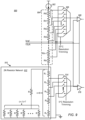
- a resistance-based temperature detector system including such a 2n resistor network will now be described with reference to the block diagram of FIG. 9 .
- the temperature detector system 900 includes a number of series connected resistors arranged in an architecture that resembles a voltage divider, but differs in that the resistances are not evenly distributed and instead of forcing a voltage a current is caused to flow through the series connected resistors.
- the current which is introduced into the series connected resistors from a current source 902 is a function of the temperature, and varies approximately linearly with changes in temperature. The temperature is measured by comparing a voltage at different nodes between the series connected resistors to a constant reference voltage (Vref).
- the series connected resistors include a first number of series connected resistors (Rt0 ⁇ Rtn) in a high range voltage-generating resistor network 904 that is connected through a first multiplexer 906 to a first comparator 908 , and a second number of series connected resistors in a low range voltage-generating resistor network 910 , which includes a 2N resistor network 912 , connected through a second multiplexer 914 to a second comparator 916 .
- high range it is meant that the high range voltage-generating resistor network 904 is capable of detecting and measuring temperature within larger or courser increments than the smaller or finer increments of the low range voltage-generating resistor network 910 .
- I I PTAT
- V TOP a voltage measured at a top node of the high range voltage-generating resistor network 904 .
- V TOP_LOW_TEMP I PTAT_LOW_TEMP ⁇ R TOP-BOT
- V TOP_HIGH_TEMP I PTAT_HIGH_TEMP ⁇ R TOP-BOT .
- the high range voltage-generating resistor network 904 and low range voltage-generating resistor network 910 are designed so when a certain temperature is crossed, the voltage generated from a specific node crosses Vref and is higher than Vref, the first or second comparator 908 , 916 connected to Vref and to the high range voltage-generating resistor network or low range voltage-generating resistor network through the associated multiplexer 906 or 914 indicates that one or more voltages that comes from the specific node has crossed Vref.
- the temperature is then determined by noting the lowest node in the high range voltage-generating resistor network 904 and low range voltage-generating resistor network 910 at which the voltage compared is still higher than Vref.
- the high range voltage-generating resistor network 904 and low range voltage-generating resistor network 910 have a different number of series connected resistors, and therefore a different total resistance, but each use substantially equally sized resistors having a substantially equal resistance of R. That is a resistance of each of the resistors (Rtn through Rt0) shown in FIG. 9 are not necessarily equal but are generated from a similar basic resistance R.
- each of the resistors is illustrated as having a resistance of R
- the overall series resistance of the combined high range voltage-generating resistor network and low range voltage-generating resistor network has a resistance of Rn+1, where the high range voltage-generating resistor network has a resistance of R ⁇ m, where m can be any number real or integer and n is used for indexing purposes, and the low range voltage-generating resistor network has a resistance of R.
- the high range voltage-generating resistor network 904 has a temperature detection resolution of 25° C., which means that the voltage at a lower node of Rtn (V RTn ) will cross Vref at 25° C.
- a temperature detector using a conventional n 2 resistor network would require an area for 64 R-sized resistors for a low range voltage-generating resistor network, while the low range voltage-generating resistor network 910 including the 2n resistor network can achieve an equivalent 5° C. resolution while occupying an area of just 16 R-sized resistors.
- the alternative resistor networks described below can gain a further area improvement over the 2n resistor network where n is an even number higher than or equal to 6. If the difference of n ⁇ 2 results in an even natural number divisible by 4, a first alternative resistor network described below with reference to FIG. 10 will result in a total number of resistors of (1.25 n+3.5), as compared to a conventional n 2 network of equal resistance resolution, and an area of (1.25 n+3.5) times the area of a single resistor. If the difference of n ⁇ 2 does not result in an even natural number divisible by 4, a second alternative resistor network described below with reference to FIG. 11 will result in a total number of resistors of (1.25n+5), as compared to a conventional n 2 network, and an area of (1.25 n+5) times the area of a single resistor.
- This first alternative resistor network 1000 includes a first resistance path 1002 with a resistor ladder 1004 including a first group of n resistors.
- a second resistance path 1006 coupled in parallel with the first resistance path and including a second resistor 1008 coupled in series with a third resistor 1010 ; and in series with a fourth group of two or more resistors 1012 coupled in parallel.
- the first group of resistors in the resistor ladder 1004 includes n or 10 resistors.
- the second and third groups of resistors 1008 , 1010 each include 1 resistor and as compared to a conventional n 2 resistor network (such as shown in FIG. 3 ) having an equivalent resolution, i.e., a 10 2 resistor network, each group replaces (n/2 ⁇ 1) ⁇ (n/2 ⁇ 1) resistors of the n 2 resistor network, or 16 resistors in the embodiment shown.
- the fourth group of resistors 1012 includes 2 resistors, which replace (n ⁇ 2)/4, or 8 resistors of the n 2 resistor network, and the fifth and sixth groups of resistors 1016 , 1018 , each include 1 resistor and replace (n/2) ⁇ (n/2), or 25 resistors of the n 2 resistor network.
- the total number of resistors in the first alternative resistor network 1000 can be calculated by summing the number of resistors in the first resistance path 1002 or n, the number of resistors in the second resistance path 1006 equal to 2+(n ⁇ 2)/4, and the number of resistors in the third resistance path 1014 .
- a second alternative resistor network where n is even natural number, greater than or equal to eight ( ⁇ 8), and where n ⁇ 2 is not divisible by 4, will now be described with reference to FIG. 11 .
- This second alternative resistor network 1100 and includes a first resistance path 1102 with a resistor ladder 1104 including a first group of n resistors, a second resistance path 1106 coupled in parallel with the first resistance path, and a third resistance path 1108 coupled in parallel with the first and second resistance paths.
- a resistor ladder 1104 including a first group of n resistors
- second resistance path 1106 coupled in parallel with the first resistance path
- a third resistance path 1108 coupled in parallel with the first and second resistance paths.
- the second resistance path 1106 includes a second resistor 1110 coupled in series with a third resistor 1112 ; and in series with a fourth group of two or more resistors 1114 coupled in parallel.
- the third resistance path 1108 includes a fifth resistor 1116 coupled in series with a sixth resistor 1118 .
- the second resistance path 1106 differs from that shown in FIG. 10 in that it further includes a seventh group 1120 of two series coupled resistors in parallel with the fourth group.
- the total number of resistors in the second alternative resistor network 1100 can be calculated by summing the number of resistors in the first resistance path 1102 or n, the number of resistors in the second resistance path 1106 equal to 2+(n ⁇ 4)/4+2, and the number of resistors in the third resistance path 1108 .
- n 12 as shown in FIG.
- the total number of equally sized resistors in the first alternative or (1.25n+5) resistor network 1100 is 20 and the area required for the network is 20RA, where RA is the area required for a single resistor.
- This represents a reduction in area of 86% over a conventional n 2 resistor network where n 12, and a 17% reduction in number of resistors and area over a 2n resistor network, which would require 24 resistors and have an area of 24RA.
- resistor network 910 may be incorporated in the low range voltage-generating resistor network 910 as best shown in FIG. 5 .
Abstract
Description
R=Rs l/w
where Rs is the sheet or bulk resistance of the patterned layer or diffusion region in ohms/square, l is a length and w is a width of conduction path through the resistor. It is important to note that two resistors having same width vs. length (W/L) ratio but not having same exact width (W) and length (L), will not have a matched resistance. Thus, in changing and more importantly in matching resistance between resistors it is generally desirable to change a number or multiplicity of matched resistors and not merely physical dimensions of the resistor.
where R is the resistance of each of the first, second and third
I=A×T,
where I is current, T is a temperature of the chip, and A is a derivative of the current and is positive (PTAT, so I is IPTAT).
Claims (11)
Priority Applications (4)
| Application Number | Priority Date | Filing Date | Title |
|---|---|---|---|
| US17/113,501 US11855641B2 (en) | 2020-07-07 | 2020-12-07 | Integrated resistor network and method for fabricating the same |
| JP2023501098A JP2023533731A (en) | 2020-07-07 | 2021-07-06 | Integrated resistor network and method of making same |
| DE112021003630.0T DE112021003630T5 (en) | 2020-07-07 | 2021-07-06 | INTEGRATED RESISTANCE NETWORK AND METHOD OF PRODUCTION |
| PCT/US2021/040419 WO2022010827A1 (en) | 2020-07-07 | 2021-07-06 | Integrated resistor network and method for fabricating the same |
Applications Claiming Priority (2)
| Application Number | Priority Date | Filing Date | Title |
|---|---|---|---|
| US202063048975P | 2020-07-07 | 2020-07-07 | |
| US17/113,501 US11855641B2 (en) | 2020-07-07 | 2020-12-07 | Integrated resistor network and method for fabricating the same |
Publications (2)
| Publication Number | Publication Date |
|---|---|
| US20220011801A1 US20220011801A1 (en) | 2022-01-13 |
| US11855641B2 true US11855641B2 (en) | 2023-12-26 |
Family
ID=79173210
Family Applications (3)
| Application Number | Title | Priority Date | Filing Date |
|---|---|---|---|
| US17/113,501 Active 2042-01-03 US11855641B2 (en) | 2020-07-07 | 2020-12-07 | Integrated resistor network and method for fabricating the same |
| US17/241,499 Active US11283434B2 (en) | 2020-07-07 | 2021-04-27 | Glitch protection system and reset scheme for secure memory devices |
| US17/241,447 Active US11671083B2 (en) | 2020-07-07 | 2021-04-27 | Voltage-glitch detection and protection circuit for secure memory devices |
Family Applications After (2)
| Application Number | Title | Priority Date | Filing Date |
|---|---|---|---|
| US17/241,499 Active US11283434B2 (en) | 2020-07-07 | 2021-04-27 | Glitch protection system and reset scheme for secure memory devices |
| US17/241,447 Active US11671083B2 (en) | 2020-07-07 | 2021-04-27 | Voltage-glitch detection and protection circuit for secure memory devices |
Country Status (5)
| Country | Link |
|---|---|
| US (3) | US11855641B2 (en) |
| JP (3) | JP2023533035A (en) |
| CN (2) | CN115769207A (en) |
| DE (3) | DE112021003633T5 (en) |
| WO (3) | WO2022010728A1 (en) |
Families Citing this family (3)
| Publication number | Priority date | Publication date | Assignee | Title |
|---|---|---|---|---|
| US11502679B2 (en) * | 2020-08-13 | 2022-11-15 | Macronix International Co., Ltd. | Robust power-on-reset circuit with body effect technique |
| US11916432B2 (en) * | 2022-01-05 | 2024-02-27 | Mediatek Inc. | Chip with power-glitch detection |
| US11727967B2 (en) * | 2022-01-13 | 2023-08-15 | Micron Technology, Inc. | Apparatuses and methods including dice latches in a semiconductor device |
Citations (41)
| Publication number | Priority date | Publication date | Assignee | Title |
|---|---|---|---|---|
| US3890610A (en) * | 1972-10-31 | 1975-06-17 | Thomson Csf | High-precision digital-to-analog converters |
| US4539553A (en) * | 1982-03-30 | 1985-09-03 | Sony Corporation | Digital-to-analog converter of the current-adding type |
| US4827222A (en) * | 1987-12-11 | 1989-05-02 | Vtc Incorporated | Input offset voltage trimming network and method |
| US5969658A (en) * | 1997-11-18 | 1999-10-19 | Burr-Brown Corporation | R/2R ladder circuit and method for digital-to-analog converter |
| US6222473B1 (en) * | 1999-04-26 | 2001-04-24 | Maxim Integrated Products, Inc. | Method and apparatus for digital to analog converters with improved switched R-2R ladders |
| US6331768B1 (en) * | 2000-06-13 | 2001-12-18 | Xicor, Inc. | High-resolution, high-precision solid-state potentiometer |
| US20020145552A1 (en) * | 2001-04-06 | 2002-10-10 | Koninklijke Philips Electronics N.V. | Digital to analogue converter |
| US20040232977A1 (en) * | 2003-01-10 | 2004-11-25 | Chao-Cheng Lee | Filter circuit |
| US20050024251A1 (en) * | 2003-07-28 | 2005-02-03 | Renesas Technology Corp. | Successive approximation analog/digital converter with reduced chip area |
| US20060284680A1 (en) * | 2005-05-18 | 2006-12-21 | Da Fonte Victor D | Amplifier arrangement and amplifying method |
| US7250890B1 (en) * | 2005-12-19 | 2007-07-31 | Maxim Integrated Products, Inc. | Area-efficient, digital variable resistor with high resolution |
| EP1814233A1 (en) * | 2006-01-18 | 2007-08-01 | Marvell World Trade Ltd. | Improved flash ADC |
| US20080303704A1 (en) * | 2005-03-31 | 2008-12-11 | Ran Ginosar | Low-Power Inverted Ladder Digital-to-Analog Converter |
| US20090140903A1 (en) * | 2004-03-27 | 2009-06-04 | Chi Mei Optoelectronics Corporation | Digital to analogue converters |
| US7619402B1 (en) * | 2008-09-26 | 2009-11-17 | Hong Kong Applied Science And Technology Research Institute Co., Ltd. | Low dropout voltage regulator with programmable on-chip output voltage for mixed signal embedded applications |
| US20110063009A1 (en) * | 2009-09-16 | 2011-03-17 | Himax Analogic, Inc. | Voltage Trimming Circuit |
| US20120200442A1 (en) * | 2011-02-08 | 2012-08-09 | Maxim Integrated Products, Inc. | Precision sub-radix2 dac with linearity calibration |
| US20130200877A1 (en) * | 2012-02-02 | 2013-08-08 | Funai Electric Co., Ltd. | Gradation voltage generating circuit and liquid crystal display device |
| US20130215540A1 (en) * | 2012-02-16 | 2013-08-22 | Newport Media, Inc. | High Voltage Electrostatic Discharge Clamp Using Deep Submicron CMOS Technology |
| US20130284811A1 (en) * | 2012-04-25 | 2013-10-31 | Ronald Steven Cok | Electronic storage system with externally-alterable conductor |
| US8581766B1 (en) * | 2011-10-17 | 2013-11-12 | Maxim Integrated Products, Inc. | DAC with novel switch regulation |
| US8618971B1 (en) * | 2012-08-03 | 2013-12-31 | Texas Instruments Incorporated | Signal level shift circuit and method for dual resistor ladder digital-to-analog converters |
| US20150236691A1 (en) * | 2014-02-18 | 2015-08-20 | Acco | Switch Controls |
| US9214950B1 (en) * | 2015-04-23 | 2015-12-15 | Lockheed Martin Corporation | Apparatus and method for temperature compensated gain and mismatch trim in subranging quantizers and analog to digital converters |
| US20160085256A1 (en) * | 2014-02-18 | 2016-03-24 | Acco | Body Biasing for RF Switch Optimization |
| US20170201827A1 (en) * | 2016-01-08 | 2017-07-13 | Samsung Electronics Co., Ltd. | Headphone driver, a sound system that incorporates the headphone driver and a computing system that incorporates the headphone driver |
| US20180300618A1 (en) * | 2017-04-14 | 2018-10-18 | Samsung Electronics Co., Ltd. | Monolithic multi-bit weight cell for neuromorphic computing |
| US10305505B1 (en) * | 2017-12-21 | 2019-05-28 | Texas Instruments Incorporated | Interpolation digital-to-analog converter (DAC) |
| US10312931B2 (en) * | 2017-09-21 | 2019-06-04 | Texas Instruments Incorporated | Programmable gain amplifier and a delta sigma analog-to-digital converter containing the PGA |
| US10374622B2 (en) * | 2018-01-05 | 2019-08-06 | Texas Instruments Incorporated | System and method for digital-to-analog converter with switched resistor networks |
| US20190305768A1 (en) * | 2018-03-28 | 2019-10-03 | Psemi Corporation | Stacked FET Switch Bias Ladders |
| US10505530B2 (en) * | 2018-03-28 | 2019-12-10 | Psemi Corporation | Positive logic switch with selectable DC blocking circuit |
| US20190379383A1 (en) * | 2018-06-07 | 2019-12-12 | International Business Machines Corporation | Using a burn-in operational amplifier for a phased locked loop regulator |
| US20200075573A1 (en) * | 2018-08-31 | 2020-03-05 | Texas Instruments Incorporated | Resistor with exponential-weighted trim |
| US20200203045A1 (en) * | 2018-12-21 | 2020-06-25 | Socionext Inc. | Voltage-divider circuits and circuitry |
| US20200201375A1 (en) * | 2018-12-17 | 2020-06-25 | Inphi Corporation | Bandgap circuits with voltage calibration |
| US20200259499A1 (en) * | 2019-02-12 | 2020-08-13 | BAE Systems Information and Electronic Systems Int egration Inc. | Circuit technique to improve spur-free dynamic range of a digital to analog converter |
| US20210250199A1 (en) * | 2020-02-06 | 2021-08-12 | Nxp B.V. | Monolithic high-voltage transceiver connected to two different supply voltage domains |
| US20210344338A1 (en) * | 2018-03-28 | 2021-11-04 | Psemi Corporation | AC Coupling Modules for Bias Ladders |
| US11271576B1 (en) * | 2021-04-06 | 2022-03-08 | Qualcomm Incorporated | Digital-to-analog converter (DAC) with common-mode correction |
| US20220206520A1 (en) * | 2020-12-30 | 2022-06-30 | Qualcomm Incorporated | Voltage reference architecture |
Family Cites Families (26)
| Publication number | Priority date | Publication date | Assignee | Title |
|---|---|---|---|---|
| US6473852B1 (en) | 1998-10-30 | 2002-10-29 | Fairchild Semiconductor Corporation | Method and circuit for performing automatic power on reset of an integrated circuit |
| US6956473B2 (en) * | 2003-01-06 | 2005-10-18 | Jbs Technologies, Llc | Self-adjusting alarm system |
| JP4130417B2 (en) * | 2004-02-27 | 2008-08-06 | 株式会社東芝 | Semiconductor integrated circuit and test method thereof |
| US20070235880A1 (en) * | 2006-03-30 | 2007-10-11 | Chin-Sheng Yang | Semiconductor device and method of fabricating the same |
| US7436245B2 (en) * | 2006-05-08 | 2008-10-14 | Exar Corporation | Variable sub-bandgap reference voltage generator |
| US20080061843A1 (en) * | 2006-09-11 | 2008-03-13 | Asier Goikoetxea Yanci | Detecting voltage glitches |
| US7501970B2 (en) * | 2006-10-30 | 2009-03-10 | Texas Instruments Incorporated | Digital to analog converter architecture and method having low switch count and small output impedance |
| US7919832B2 (en) * | 2007-01-11 | 2011-04-05 | Taiwan Semiconductor Manufacturing Co., Ltd. | Stack resistor structure for integrated circuits |
| US8947282B1 (en) * | 2010-01-20 | 2015-02-03 | Ikanos Communications, Inc. | Method and apparatus for a current control |
| US8344767B2 (en) | 2010-10-14 | 2013-01-01 | Fairchild Semiconductor Corporation | Low power power-on-reset (POR) circuit |
| US9143137B2 (en) * | 2012-02-10 | 2015-09-22 | Freescale Semiconductor, Inc. | Low voltage CMOS power on reset circuit |
| TW201413415A (en) * | 2012-09-28 | 2014-04-01 | Novatek Microelectronics Corp | Reference voltage generator |
| US9018989B2 (en) * | 2012-10-24 | 2015-04-28 | Stmicroelectronics International N.V. | Power-on-reset and supply brown out detection circuit with programmability |
| TW201417496A (en) * | 2012-10-24 | 2014-05-01 | Keystone Semiconductor Corp | Power-supply opening reset circuit |
| FR3003071B1 (en) | 2013-03-06 | 2016-11-11 | Inside Secure | MEMORY COMPRISING A CIRCUIT FOR DETECTING A TRANSIENT IMPULSE ON A MEMORY LINE |
| US8884799B2 (en) * | 2013-03-15 | 2014-11-11 | Qualcomm Incroporated | Dual-string digital-to-analog converters (DACs), and related circuits, systems, and methods |
| US9541603B2 (en) | 2013-07-10 | 2017-01-10 | Apple Inc. | Method and apparatus for power glitch detection in integrated circuits |
| CN104811171B (en) | 2014-01-26 | 2018-01-09 | 京微雅格(北京)科技有限公司 | The electrification reset circuit of zero current |
| US9523722B2 (en) * | 2014-06-02 | 2016-12-20 | Winbond Electronics Corporation | Method and apparatus for supply voltage glitch detection in a monolithic integrated circuit device |
| US9397654B2 (en) | 2014-10-09 | 2016-07-19 | Qualcomm Incorporated | Low power externally biased power-on-reset circuit |
| US10436856B2 (en) * | 2015-12-24 | 2019-10-08 | Asahi Kasei Microdevices Corporation | Magnetic sensor apparatus and current sensor apparatus |
| US9984763B1 (en) * | 2016-11-30 | 2018-05-29 | Nxp Usa, Inc. | Sample and hold circuit |
| US10726122B2 (en) * | 2017-07-03 | 2020-07-28 | Nxp B.V. | Automatic reset filter deactivation during critical security processes |
| US10586584B2 (en) * | 2018-06-01 | 2020-03-10 | Samsung Electronics Co., Ltd. | Semiconductor semiconductor memory devices, memory systems and methods of operating memory devices |
| US10466275B1 (en) * | 2018-06-28 | 2019-11-05 | Xilinx, Inc. | Glitch detector and test glitch generator |
| US11443073B2 (en) * | 2018-12-17 | 2022-09-13 | Intel Corporation | Techniques for preventing voltage tampering of security control circuits |
-
2020
- 2020-12-07 US US17/113,501 patent/US11855641B2/en active Active
-
2021
- 2021-04-27 US US17/241,499 patent/US11283434B2/en active Active
- 2021-04-27 US US17/241,447 patent/US11671083B2/en active Active
- 2021-07-01 WO PCT/US2021/040060 patent/WO2022010728A1/en active Application Filing
- 2021-07-01 DE DE112021003633.5T patent/DE112021003633T5/en active Pending
- 2021-07-01 CN CN202180047971.XA patent/CN115769207A/en active Pending
- 2021-07-01 JP JP2023501211A patent/JP2023533035A/en active Pending
- 2021-07-02 WO PCT/US2021/040222 patent/WO2022010754A1/en active Application Filing
- 2021-07-02 CN CN202180047951.2A patent/CN115868114B/en active Active
- 2021-07-02 JP JP2023501099A patent/JP2023533972A/en active Pending
- 2021-07-02 DE DE112021003640.8T patent/DE112021003640T5/en active Pending
- 2021-07-06 JP JP2023501098A patent/JP2023533731A/en active Pending
- 2021-07-06 DE DE112021003630.0T patent/DE112021003630T5/en active Pending
- 2021-07-06 WO PCT/US2021/040419 patent/WO2022010827A1/en active Application Filing
Patent Citations (41)
| Publication number | Priority date | Publication date | Assignee | Title |
|---|---|---|---|---|
| US3890610A (en) * | 1972-10-31 | 1975-06-17 | Thomson Csf | High-precision digital-to-analog converters |
| US4539553A (en) * | 1982-03-30 | 1985-09-03 | Sony Corporation | Digital-to-analog converter of the current-adding type |
| US4827222A (en) * | 1987-12-11 | 1989-05-02 | Vtc Incorporated | Input offset voltage trimming network and method |
| US5969658A (en) * | 1997-11-18 | 1999-10-19 | Burr-Brown Corporation | R/2R ladder circuit and method for digital-to-analog converter |
| US6222473B1 (en) * | 1999-04-26 | 2001-04-24 | Maxim Integrated Products, Inc. | Method and apparatus for digital to analog converters with improved switched R-2R ladders |
| US6331768B1 (en) * | 2000-06-13 | 2001-12-18 | Xicor, Inc. | High-resolution, high-precision solid-state potentiometer |
| US20020145552A1 (en) * | 2001-04-06 | 2002-10-10 | Koninklijke Philips Electronics N.V. | Digital to analogue converter |
| US20040232977A1 (en) * | 2003-01-10 | 2004-11-25 | Chao-Cheng Lee | Filter circuit |
| US20050024251A1 (en) * | 2003-07-28 | 2005-02-03 | Renesas Technology Corp. | Successive approximation analog/digital converter with reduced chip area |
| US20090140903A1 (en) * | 2004-03-27 | 2009-06-04 | Chi Mei Optoelectronics Corporation | Digital to analogue converters |
| US20080303704A1 (en) * | 2005-03-31 | 2008-12-11 | Ran Ginosar | Low-Power Inverted Ladder Digital-to-Analog Converter |
| US20060284680A1 (en) * | 2005-05-18 | 2006-12-21 | Da Fonte Victor D | Amplifier arrangement and amplifying method |
| US7250890B1 (en) * | 2005-12-19 | 2007-07-31 | Maxim Integrated Products, Inc. | Area-efficient, digital variable resistor with high resolution |
| EP1814233A1 (en) * | 2006-01-18 | 2007-08-01 | Marvell World Trade Ltd. | Improved flash ADC |
| US7619402B1 (en) * | 2008-09-26 | 2009-11-17 | Hong Kong Applied Science And Technology Research Institute Co., Ltd. | Low dropout voltage regulator with programmable on-chip output voltage for mixed signal embedded applications |
| US20110063009A1 (en) * | 2009-09-16 | 2011-03-17 | Himax Analogic, Inc. | Voltage Trimming Circuit |
| US20120200442A1 (en) * | 2011-02-08 | 2012-08-09 | Maxim Integrated Products, Inc. | Precision sub-radix2 dac with linearity calibration |
| US8581766B1 (en) * | 2011-10-17 | 2013-11-12 | Maxim Integrated Products, Inc. | DAC with novel switch regulation |
| US20130200877A1 (en) * | 2012-02-02 | 2013-08-08 | Funai Electric Co., Ltd. | Gradation voltage generating circuit and liquid crystal display device |
| US20130215540A1 (en) * | 2012-02-16 | 2013-08-22 | Newport Media, Inc. | High Voltage Electrostatic Discharge Clamp Using Deep Submicron CMOS Technology |
| US20130284811A1 (en) * | 2012-04-25 | 2013-10-31 | Ronald Steven Cok | Electronic storage system with externally-alterable conductor |
| US8618971B1 (en) * | 2012-08-03 | 2013-12-31 | Texas Instruments Incorporated | Signal level shift circuit and method for dual resistor ladder digital-to-analog converters |
| US20150236691A1 (en) * | 2014-02-18 | 2015-08-20 | Acco | Switch Controls |
| US20160085256A1 (en) * | 2014-02-18 | 2016-03-24 | Acco | Body Biasing for RF Switch Optimization |
| US9214950B1 (en) * | 2015-04-23 | 2015-12-15 | Lockheed Martin Corporation | Apparatus and method for temperature compensated gain and mismatch trim in subranging quantizers and analog to digital converters |
| US20170201827A1 (en) * | 2016-01-08 | 2017-07-13 | Samsung Electronics Co., Ltd. | Headphone driver, a sound system that incorporates the headphone driver and a computing system that incorporates the headphone driver |
| US20180300618A1 (en) * | 2017-04-14 | 2018-10-18 | Samsung Electronics Co., Ltd. | Monolithic multi-bit weight cell for neuromorphic computing |
| US10312931B2 (en) * | 2017-09-21 | 2019-06-04 | Texas Instruments Incorporated | Programmable gain amplifier and a delta sigma analog-to-digital converter containing the PGA |
| US10305505B1 (en) * | 2017-12-21 | 2019-05-28 | Texas Instruments Incorporated | Interpolation digital-to-analog converter (DAC) |
| US10374622B2 (en) * | 2018-01-05 | 2019-08-06 | Texas Instruments Incorporated | System and method for digital-to-analog converter with switched resistor networks |
| US20210344338A1 (en) * | 2018-03-28 | 2021-11-04 | Psemi Corporation | AC Coupling Modules for Bias Ladders |
| US20190305768A1 (en) * | 2018-03-28 | 2019-10-03 | Psemi Corporation | Stacked FET Switch Bias Ladders |
| US10505530B2 (en) * | 2018-03-28 | 2019-12-10 | Psemi Corporation | Positive logic switch with selectable DC blocking circuit |
| US20190379383A1 (en) * | 2018-06-07 | 2019-12-12 | International Business Machines Corporation | Using a burn-in operational amplifier for a phased locked loop regulator |
| US20200075573A1 (en) * | 2018-08-31 | 2020-03-05 | Texas Instruments Incorporated | Resistor with exponential-weighted trim |
| US20200201375A1 (en) * | 2018-12-17 | 2020-06-25 | Inphi Corporation | Bandgap circuits with voltage calibration |
| US20200203045A1 (en) * | 2018-12-21 | 2020-06-25 | Socionext Inc. | Voltage-divider circuits and circuitry |
| US20200259499A1 (en) * | 2019-02-12 | 2020-08-13 | BAE Systems Information and Electronic Systems Int egration Inc. | Circuit technique to improve spur-free dynamic range of a digital to analog converter |
| US20210250199A1 (en) * | 2020-02-06 | 2021-08-12 | Nxp B.V. | Monolithic high-voltage transceiver connected to two different supply voltage domains |
| US20220206520A1 (en) * | 2020-12-30 | 2022-06-30 | Qualcomm Incorporated | Voltage reference architecture |
| US11271576B1 (en) * | 2021-04-06 | 2022-03-08 | Qualcomm Incorporated | Digital-to-analog converter (DAC) with common-mode correction |
Also Published As
| Publication number | Publication date |
|---|---|
| DE112021003633T5 (en) | 2023-04-20 |
| US20220011801A1 (en) | 2022-01-13 |
| WO2022010827A1 (en) | 2022-01-13 |
| DE112021003640T5 (en) | 2023-05-04 |
| WO2022010728A1 (en) | 2022-01-13 |
| CN115868114B (en) | 2023-08-18 |
| CN115769207A (en) | 2023-03-07 |
| JP2023533972A (en) | 2023-08-07 |
| US11283434B2 (en) | 2022-03-22 |
| US11671083B2 (en) | 2023-06-06 |
| JP2023533731A (en) | 2023-08-04 |
| DE112021003630T5 (en) | 2023-04-27 |
| WO2022010754A1 (en) | 2022-01-13 |
| US20220014181A1 (en) | 2022-01-13 |
| JP2023533035A (en) | 2023-08-01 |
| CN115868114A (en) | 2023-03-28 |
| US20220014180A1 (en) | 2022-01-13 |
Similar Documents
| Publication | Publication Date | Title |
|---|---|---|
| US11855641B2 (en) | Integrated resistor network and method for fabricating the same | |
| US4258311A (en) | Constant voltage generator for generating a constant voltage having a predetermined temperature coefficient | |
| EP2248172B1 (en) | Resistor triggered electrostatic discharge protection | |
| US5448103A (en) | Temperature independent resistor | |
| US5281872A (en) | Current detectable transistor having sense resistor with particular temperature coefficient | |
| JP2003133428A (en) | Driving method for semiconductor element | |
| US8604589B2 (en) | Semiconductor device of polycrystalline silicon resistors | |
| US10508958B2 (en) | Semiconductor pressure sensor with piezo-resistive portions with conductive shields | |
| US20160111631A1 (en) | Vertical hall sensors with reduced offset error | |
| GB2092374A (en) | Variable capacitor | |
| WO2001063662A2 (en) | Resistor arrays for mask-alignment detection | |
| CN100539145C (en) | Resistance circuit | |
| US6144040A (en) | Van der pauw structure to measure the resistivity of a doped area under diffusion areas and gate structures | |
| US4449141A (en) | Variable capacitor | |
| JP2006269573A (en) | Semiconductor device | |
| US5473250A (en) | Hall-effect sensor having reduced edge effects and improved sensitivity | |
| US11422208B2 (en) | Magnetic sensor | |
| US6768139B2 (en) | Transistor configuration for a bandgap circuit | |
| JPH01220867A (en) | Semiconductor with carrier capacity reading part and integrated dc voltage supply part | |
| JPH09162459A (en) | Differential semiconductor thin film magnetoresistive device | |
| JPH0422164A (en) | Semiconductor device equipped with temperature detection function | |
| US20020033518A1 (en) | Integrated circuit resistor structure | |
| JP4234216B2 (en) | Silicon controlled rectifier and high voltage SCR switch | |
| JPS63157461A (en) | Semiconductor device | |
| JPH08330516A (en) | Semiconductor device and stabilized power supply circuit |
Legal Events
| Date | Code | Title | Description |
|---|---|---|---|
| AS | Assignment |
Owner name: INFINEON TECHNOLOGIES LLC, CALIFORNIA Free format text: ASSIGNMENT OF ASSIGNORS INTEREST;ASSIGNOR:SHLOMO, OREN;REEL/FRAME:054564/0413 Effective date: 20201207 |
|
| FEPP | Fee payment procedure |
Free format text: ENTITY STATUS SET TO UNDISCOUNTED (ORIGINAL EVENT CODE: BIG.); ENTITY STATUS OF PATENT OWNER: LARGE ENTITY |
|
| STPP | Information on status: patent application and granting procedure in general |
Free format text: DOCKETED NEW CASE - READY FOR EXAMINATION |
|
| STPP | Information on status: patent application and granting procedure in general |
Free format text: RESPONSE TO NON-FINAL OFFICE ACTION ENTERED AND FORWARDED TO EXAMINER |
|
| STPP | Information on status: patent application and granting procedure in general |
Free format text: NOTICE OF ALLOWANCE MAILED -- APPLICATION RECEIVED IN OFFICE OF PUBLICATIONS |
|
| STPP | Information on status: patent application and granting procedure in general |
Free format text: PUBLICATIONS -- ISSUE FEE PAYMENT RECEIVED |
|
| STPP | Information on status: patent application and granting procedure in general |
Free format text: PUBLICATIONS -- ISSUE FEE PAYMENT VERIFIED |
|
| STCF | Information on status: patent grant |
Free format text: PATENTED CASE |