US11831739B2 - Communication apparatus and communication system - Google Patents
Communication apparatus and communication system Download PDFInfo
- Publication number
- US11831739B2 US11831739B2 US17/241,614 US202117241614A US11831739B2 US 11831739 B2 US11831739 B2 US 11831739B2 US 202117241614 A US202117241614 A US 202117241614A US 11831739 B2 US11831739 B2 US 11831739B2
- Authority
- US
- United States
- Prior art keywords
- signal
- master
- slave
- serdes
- mode
- Prior art date
- Legal status (The legal status is an assumption and is not a legal conclusion. Google has not performed a legal analysis and makes no representation as to the accuracy of the status listed.)
- Active, expires
Links
Images


Classifications
-
- H—ELECTRICITY
- H04—ELECTRIC COMMUNICATION TECHNIQUE
- H04L—TRANSMISSION OF DIGITAL INFORMATION, e.g. TELEGRAPHIC COMMUNICATION
- H04L69/00—Network arrangements, protocols or services independent of the application payload and not provided for in the other groups of this subclass
- H04L69/08—Protocols for interworking; Protocol conversion
-
- G—PHYSICS
- G06—COMPUTING OR CALCULATING; COUNTING
- G06F—ELECTRIC DIGITAL DATA PROCESSING
- G06F13/00—Interconnection of, or transfer of information or other signals between, memories, input/output devices or central processing units
- G06F13/38—Information transfer, e.g. on bus
- G06F13/42—Bus transfer protocol, e.g. handshake; Synchronisation
- G06F13/4282—Bus transfer protocol, e.g. handshake; Synchronisation on a serial bus, e.g. I2C bus, SPI bus
-
- H—ELECTRICITY
- H04—ELECTRIC COMMUNICATION TECHNIQUE
- H04L—TRANSMISSION OF DIGITAL INFORMATION, e.g. TELEGRAPHIC COMMUNICATION
- H04L1/00—Arrangements for detecting or preventing errors in the information received
- H04L1/12—Arrangements for detecting or preventing errors in the information received by using return channel
- H04L1/16—Arrangements for detecting or preventing errors in the information received by using return channel in which the return channel carries supervisory signals, e.g. repetition request signals
- H04L1/1607—Details of the supervisory signal
Definitions
- the present disclosure relates to a communication apparatus and a communication system.
- a technology for performing, when data communication is performed between a master apparatus and a slave apparatus, serial communication between a SerDes apparatus for the master apparatus and a SerDes apparatus for the slave apparatus has been proposed.
- the slave apparatus In the case where the slave apparatus receives data transmitted from the master apparatus, it is common for the slave apparatus to transmit, to the master apparatus, an ACK signal indicating that the data has been received.
- the present disclosure provides a communication apparatus and a communication system capable of efficiently performing data communication.
- a communication apparatus including:
- a LINK for performing protocol-conversion on a signal from a Master and outputting the converted signal to a Slave SerDes and for performing protocol-conversion on a signal from the Slave SerDes and outputting the converted signal to the Master, in which
- the LINK is capable of alternatively selecting a first mode and a second mode when transmitting the signal from the Master to the Slave SerDes,
- a signal to be transmitted to the Slave SerDes includes command information indicating content transmitted from the Master, and
- a signal to be transmitted to the Master includes command information indicating content transmitted from the Slave SerDes.
- the number of bytes of the signal to be transmitted to the Slave SerDes in the first mode may be one of 2 bytes and 3 bytes except for clock frequency information and error correction code.
- the LINK may
- the LINK may
- the LINK may
- the LINK may
- the LINK may
- the LINK may
- the LINK may
- the command information may include at least one of
- third information indicating, where the first mode is selected, whether or not one of writing data and reading data is included
- sixth information indicating, where the first mode is selected, whether or not a Stop Condition instructing to stop transmission of information is included, or
- the LINK may transmit the signal including the seventh information to the Slave SerDes, and then transmit the signal including the address information of the final destination apparatus to the Slave SerDes.
- the LINK may transmit a signal obtained by combining the seventh information and the address information of the final destination apparatus to the Slave SerDes.
- Each of the signal to the Slave SerDes and the signal to the Master may include, in addition to the command information, at least one of an error correction code, data, clock frequency information, or information indicating a type of a command to be transmitted and received.
- the signal to the Slave SerDes may include at least one of
- the command information may include, where the second mode is selected, command-format information defined by the first communication standard, and
- the command-format information may include an error command format.
- the command information may include, where the second mode is selected, data-end-determination-condition information for specifying a condition for determining an end of the signal transmitted from the Master.
- Each of the signal to the Slave SerDes and the signal from the Slave SerDes may include a command obtained by performing protocol conversion on a command of I2C (Inter-Integrated Circuit) communication into a command of the first communication standard.
- I2C Inter-Integrated Circuit
- the protocol conversion by the LINK may be protocol conversion of TDD (Time Division Duplex).
- a communication apparatus including:
- a LINK for performing protocol-conversion on a signal from a Master SerDes and outputting the converted signal to a Slave and for performing protocol-conversion on a signal from the Slave and outputting the converted signal to the Master SerDes, in which
- the LINK is capable of alternatively selecting a first mode and a second mode when transmitting the signal from the Master SerDes to the Slave,
- a signal from the Master SerDes includes command information indicating content transmitted from the Master SerDes
- a signal from the Slave includes command information indicating content transmitted from the Slave.
- a communication system including:
- the first LINK is capable of alternatively selecting a first mode and a second mode when transmitting the signal from a Master to the Slave SerDes,
- a signal to be transmitted to the Slave SerDes includes command information indicating content transmitted from the Master
- a signal to be transmitted to the Master includes command information indicating content transmitted from the Slave SerDes,
- the second LINK is capable of alternatively selecting a first mode and a second mode when transmitting the signal from the Master SerDes to the Slave,
- a signal from the Master SerDes includes command information indicating content transmitted from the Master SerDes
- a signal from the Slave includes command information indicating content transmitted from the Slave.
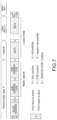
- FIG. 1 is a block diagram showing a schematic configuration of a communication system including a communication apparatus according to an embodiment
- FIG. 2 is a block diagram of a more specific one of the communication system shown in FIG. 1 ;
- FIG. 3 is a diagram showing a write format of a packet in the case where writing is performed through I2C communication between a Master and a Slave via a general SerDes device;
- FIG. 4 is an equivalent block diagram in the case where a Master SerDes performs I2C communication between a Master and a Slave SerDes;
- FIG. 5 is an equivalent block diagram in the case where the Slave SerDes performs I2C communication between the Slave and the Master SerDes;
- FIG. 6 is a diagram showing an example of a frame structure of a signal of a communication standard X protocol
- FIG. 7 is a diagram showing an I2C communication protocol at the time of Random Write
- FIG. 8 is a timing chart where I2C communication is performed between the Master and the Slave by an FDD method
- FIG. 9 A is a timing chart of a Bulk I2C mode by a TDD method
- FIG. 9 B is a timing chart of a Byte I2C mode by the TDD method
- FIG. 10 A is a diagram showing an example of a cmd_mode in the Bulk I2C mode
- FIG. 10 B is a diagram showing an example of the cmd_mode in the Byte I2C mode
- FIG. 11 A is a diagram showing a first example of a command format transmitted and received through I2C communication when the Bulk I2C mode is selected;
- FIG. 11 B is a diagram showing a second example of the command format transmitted and received through I2C communication when the Bulk I2C mode is selected;
- FIG. 11 C is a diagram showing a third example of the command format transmitted and received through I2C communication when the Bulk I2C mode is selected;
- FIG. 11 D is a diagram describing a method of calculating the position of an End of Data in the third example of FIG. 11 C ;
- FIG. 11 E is a diagram showing a first example of a command format when the Byte I2C mode is selected.
- FIG. 11 F is a diagram showing a second example of the command format when the Byte I2C mode is selected.
- FIG. 12 is a diagram showing a type and bit strings of a command transmitted over the communication standard X protocol
- FIG. 13 A is a diagram showing an example of setting the cmd-mode in the case where condition information and an instruction for the Slave SerDes to automatically generate a clock CLK count are transmitted in the Byte I2C mode;
- FIG. 13 B is a diagram showing an example of setting the cmd-mode in the case where data and an instruction for the Slave SerDes to automatically generate a clock CLK count are transmitted in the Byte I2C mode;
- FIG. 14 A is a diagram showing an example 1 of setting the cmd-mode in the case where the condition information, the data, and the specification of the clock CLK count generated by the Slave SerDes are transmitted in the Byte I2C mode;
- FIG. 14 B is a diagram showing an example 2 of setting the cmd-mode in the case where the condition information, the data, and the specification of the clock CLK count generated by the Slave SerDes are transmitted in the Byte I2C mode;
- FIG. 15 A is a diagram showing an example of transmitting ACK and data in the Byte I2C mode
- FIG. 15 B is a diagram showing an example of transmitting NACK and a STOP command in the Byte I2C mode
- FIG. 16 is a diagram showing an example of setting the cmd_mode in the case where an error has occurred
- FIG. 17 is a state transition diagram of the Master SerDes that is a node 1 and the Slave SerDes that is a node 2 ;
- FIG. 18 is a timing chart of a basic Write model in which the Slave SerDes automatically generates a clock CLK count in the Byte I2C mode;
- FIG. 19 is a timing chart of a Write operation 2 that is a modified example of the Write operation 1 shown in FIG. 18 ;
- FIG. 20 is a timing chart of a basic Write operation 3 for specifying a clock CLK count in the Byte I2C mode;
- FIG. 21 is a timing chart of a Write operation 4 that is a modified example of the Write operation 3 shown in FIG. 20 ;
- FIG. 22 is a timing chart of a basic Read model in which the Slave SerDes automatically generates a clock CLK count in the Byte I2C mode;
- FIG. 23 is a timing chart of a Read operation 2 that is a modified example of the Read operation 1 shown in FIG. 22 ;
- FIG. 24 is a timing chart of a Read operation 3 in the case where there is no Sub Address
- FIG. 25 is a timing chart of an Err operation 1 in the Byte I2C mode
- FIG. 26 is a timing chart of an Err operation 2 in the Byte I2C mode
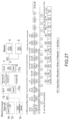
- FIG. 27 is a diagram showing a signal transmitted and received between the Master and the Master SerDes in the Bulk I2C mode
- FIG. 28 is a diagram showing an example of data stored in a table 1 in a mem 1 in the Bulk I2C mode
- FIG. 29 is a diagram showing processing of transmitting a Random Write Command from the Master SerDes to the Slave SerDes in the Bulk I2C mode over the communication standard X;
- FIG. 30 is a diagram showing an example of a table 3 in a mem 2 at the time of the Random Write operation in the Bulk I2C mode;
- FIG. 31 is a diagram showing processing in which the Slave SerDes and the Slave transmit and receive data to/from each other through I2C communication in the Bulk I2C mode;
- FIG. 32 is a diagram showing processing of replying from the Slave SerDes to the Master SerDes in response to a Random Write Command over the communication protocol X in the Bulk I2C mode;
- FIG. 33 is a diagram showing the state of a storage area of a mem 2 before releasing the storage area in response to the Random Write Command in the Bulk I2C mode;
- FIG. 34 is a diagram showing an operation of the Master SerDes in the Bulk I2C mode
- FIG. 35 is a diagram showing a state table 1 of the mem 1 after receiving reply data from the Slave SerDes in response to the Random Write Command in the Bulk I2C mode;
- FIG. 36 is a diagram showing processing in the case where the Master polls the Master SerDes for the Random Write Command in the Bulk I2C mode and reads the result;
- FIG. 37 is a diagram showing transmission of a signal for the Master to release, in the Bulk I2C mode, the storage area of the mem 1 for the Master SerDes as Random Write operation finishing processing;
- FIG. 38 is a diagram showing stored data in the mem 1 before the storage area is released in response to the Random Write Command in the Bulk I2C mode;
- FIG. 40 is a diagram following FIG. 39 ;
- FIG. 42 is a diagram showing a Random Read operation in the Bulk I2C mode
- FIG. 43 is a diagram showing stored data of the table 1 in the mem 1 at the time of the Random Read operation in the Bulk I2C mode;
- FIG. 44 is a diagram showing processing of transmitting, in the Bulk I2C mode, the Random Read command from the Master SerDes to the Slave SerDes over the communication protocol X;
- FIG. 45 is a diagram showing stored data in a table 3 in the mem 2 at the time of the Random Read operation in the Bulk I2C mode;
- FIG. 46 A is a diagram showing processing of transmitting and receiving the random read command from the Slave SerDes to the Slave in the Bulk I2C mode;
- FIG. 46 B is a diagram showing an I2C communication protocol at the time of the Random Read operation
- FIG. 47 is a diagram showing stored data of the table 3 in the mem 2 after the Random Read operation in the Bulk I2C mode;
- FIG. 48 is a diagram showing processing of replying in response to the Read command from the Slave SerDes to the Master SerDes over the communication standard X over the Bulk I2C mode;
- FIG. 49 is a diagram showing processing of the Master SerDes when receiving reply from the Slave SerDes in response to the Random Read Command in the Bulk I2C mode;
- FIG. 50 is a diagram showing an example of data in the mem 1 after receiving reply data from the Slave SerDes in response to the Random Read Command in the Bulk I2C mode;
- FIG. 51 is a diagram showing processing in the case where the Master polls the Master SerDes for the Random Read Command in the Bulk I2C mode and reads the result;
- FIG. 52 is a diagram showing an example of stored data of the table 1 in the mem 1 before releasing the storage area in response to the Random Read Command in the Bulk I2C mode;
- FIG. 53 A is a diagram showing processing on the Slave SerDes side in the case where Current read is performed in the Bulk I2C mode;
- FIG. 53 B is a diagram showing an I2C communication protocol in the case where the Current read is performed.
- FIG. 54 is a diagram showing an example of stored data of the table 3 in the mem 2 in the case where the Random Read Command is performed in the Bulk I2C mode;
- FIG. 55 is a timing chart of a Read operation in the normal state of the Bulk I2C mode
- FIG. 56 is a diagram showing an example in which an ACK/NACK signal is not transmitted from the Slave during the limited time in the Bulk I2C mode;
- FIG. 57 is a diagram showing stored data of the table 3 in the mem 2 when the Slave SerDes has transmitted the error command format in the Bulk I2C mode;
- FIG. 58 is a diagram showing stored data of the table 1 in the mem 1 when the Master SerDes has received the error command format in the Bulk I2C mode;
- FIG. 59 is a timing chart of the case where an error has occurred during Read in the Bulk I2C mode (hereinafter, the Read error case 2 );
- FIG. 60 is a diagram showing stored data of the table 1 in the mem 1 of the node 1 in the Read error case 2 ;
- FIG. 61 is a diagram showing stored data of the table 1 in the mem 1 of the node 1 in a Write error case.
- FIG. 62 is an equivalent block diagram of a communication system according to this embodiment.
- FIG. 1 is a block diagram showing a schematic configuration of a communication system including a communication apparatus according to an embodiment
- FIG. 2 is a block diagram of a more specific one of the communication system shown in FIG. 1 .
- the communication system shown in FIG. 1 and FIG. 2 is, for example, a camera video recognition system that is a part of an ADAS (Advanced Driver Assistance System).
- ADAS Advanced Driver Assistance System
- the communication apparatus shown in FIG. 1 and FIG. 2 includes an ECU 4 and a SoC 5 that are operable as a Master 21 , an image sensor 12 and a temperature sensor 14 that are operable as a Slave 22 , a Master SerDes 7 , and a Slave SerDes 13 .
- the Master SerDes 7 and the Slave SerDes 13 are connected to each other so as to be capable of communicating with each other over a predetermined communication standard (hereinafter, referred to as the “communication standard X”).
- the predetermined communication standard X include, but are not limited to, FPD-Link III, A-phy, and ASA.
- Each of the Master SerDes 7 and the Slave SerDes 13 corresponds to the communication apparatus according to this embodiment.
- the Master SerDes 7 is referred to as the SerDes 1
- the Slave SerDes 13 is referred to as the SerDes 2 in some cases.
- the Master 21 and the Master SerDes 7 are connected to each other so as to be capable of communicating with each other through, for example, I2C (Inter-Integrated Circuit) communication.
- I2C Inter-Integrated Circuit
- the communication between the Master 21 and the Master SerDes 7 is not limited to the I2C communication, and may be, for example, communication using GPIO (General Purpose Input/Output).
- the Slave 22 and the Slave SerDes 13 are connected to each other so as to be capable of communicating with each other through, for example, I2C communication.
- I2C communication for example, I2C communication.
- the communication between the Slave 22 and the Slave SerDes 13 is not limited to the I2C communication, and may be, for example, communication using GPIO.
- a signal path on a transmission path 6 for performing serial transmission on information from the Slave SerDes 13 to the Master SerDes 7 is referred to as the downlink or the forward channel
- a signal path on the transmission path 6 for performing serial transmission on information from the Master SerDes 7 to the Slave SerDes 13 is referred to as the uplink or the reverse channel.
- the ECU 4 controls the entire communication system 3 and includes an I2C 4 a .
- the ECU 4 receives an image signal from the Master SerDes 7 and performs I2C communication with the Master SerDes 7 via the I2C 4 a.
- the SoC 5 performs, for example, image recognition or video processing, and includes an I2C 5 a .
- the SoC 5 receives an image signal from the Master SerDes 7 and performs I2C communication with the Master SerDes 7 via the I2C 5 a.
- the image sensor 12 captures an image and includes an I2C 12 a and a mem 19 .
- the image sensor 12 outputs image data of the captured image to the Slave SerDes 13 and performs I2C communication with the Slave SerDes 13 through the I2C 12 a .
- the image sensor 12 is referred to as the CIS (CMOS image sensor) in some cases.
- the mem 19 is capable of storing pixel data obtained by capturing by the image sensor 12 or storing data transmitted from the Master 21 .
- the mem 19 is referred to as the mem 3 in some cases.
- the temperature sensor 14 measures the temperature of an arbitrary target (e.g., the image sensor 12 ) and includes an I2C 14 a .
- the temperature sensor 14 performs I2C communication with the Slave SerDes 13 via the I2C 14 a , and transmits temperature data relating to the measured temperature, or the like to the Slave SerDes 13 .
- the Master SerDes 7 converts the signal of the I2C protocol received from the Master 21 into a signal of the communication standard X protocol, transmits the converted signal to the Slave SerDes 13 , and appropriately performs format conversion on the signal of the communication standard X protocol received from the Slave SerDes 13 to generate image data or a signal of the I2C protocol, and outputs the generated data or signal to the Master 21 .
- This Master SerDes 7 includes a LINK 11 , a forward receiver (Fw.Rx) 9 , a reverse transmitter (Rv.Tx) 10 , and an I2C 7 a.
- the LINK 11 performs format conversion on the signal of the I2C protocol received from the Master 21 via the I2C 7 a into a signal of the communication standard X protocol, and transmits the converted signal to the Slave SerDes 13 via the Rv.Tx 10 . Further, the LINK 11 generates image data from the signal of the communication standard X protocol received from the Slave SerDes 13 via the Fw.Rx 9 and transmits the generated data to the Master 21 , or generates a signal of the I2C protocol including information other than image data and outputs the generates signal to the Master 21 via the I2C 7 a.
- the Slave SerDes 13 performs format conversion on the signal of the I2C protocol or the image signal received from the Slave 22 into a signal of the communication standard X protocol and transmits the converted signal to the Master SerDes 7 , and appropriately performs format conversion on the signal of the communication standard X protocol received from the Master SerDes 7 into a signal of the I2C protocol and outputs the converted signal to the Slave 22 .
- This Slave SerDes 13 includes a LINK 17 , a forward transmitter (Fw.Tx) 16 , a reverse receiver (Rv.Rx) 15 , and an I2C 13 a.
- the LINK 17 performs format conversion on the signal of the I2C protocol or the image data received from the Slave 22 via the I2C 13 a into a signal of the communication standard X protocol and transmits the converted signal to the Master SerDes 7 via the Fw.Tx 16 . Further, the LINK 17 converts the signal of the communication standard X protocol received from the Master SerDes 7 via the Rv.Rx 15 into a signal of the I2C standard and transmits the converted signal to the Slave 22 via the I2C 13 a . At this time, there is a possibility that the following problems 1) and 2) occur.
- the Master 21 needs to receive an ACK signal or a NACK signal from the Slave 22 every time the Master 21 transmits information in units of one byte or the like.
- the propagation delay of I2C communication via the Master SerDes 7 and the Slave SerDes 13 is generally larger than the period of one clock of I2C communication (e.g., 400 kH or 1 MHz for a frequency of one clock) in some cases.
- the Master SerDes 7 receives, from the Slave SerDes 13 , the ACK signal or the NACK signal from the Slave 22 and holds the clock (SCL) of the I2C protocol signal at a Low level until the I2C protocol conversion is completed and it is ready to output the ACK signal or the NACK signal to the Master 21 via the I2C 7 a .
- the Master SerDes 7 releases the held Low level of the clock (SCL) of the I2C protocol signal after it is ready to output the ACK signal or the NACK signal transmitted from the Slave 22 to the Master 21 .
- the Master 21 is capable of resuming I2C communication and receiving the ACK signal or the NACK signal.
- FIG. 3 shows I2C communication in the case where writing is performed from a HOST I2C (e.g., the Master 21 ) to a REMOTE I2C (e.g., the Slave 22 ) via the Master SerDes 7 and a Slave SerDes 13 through I2C communication.
- the SCL low period of the HOST I2C indicates that the SCL is held at the low level until the Master SerDes 7 is ready to output the ACK signal or the NACK signal from a Slave 22 and the HOST I2C cannot perform I2C communication during this period.
- the Slave SerDes 13 is assumed to perform I2C communication with the various Slaves 22 , and the I2C operation clock of the Slave 22 (operation clock of I2C communication between the Slave 22 and the Slave SerDes 13 ) is set lower than required in some cases.
- the I2C operation clock frequency of the Slave 22 in the case where the I2C operation clock frequency of the Slave 22 is set to be lower than required as described above, it means that the I2C operation period of the REMOTE I2C (period other than the SCL low on the REMOTE I2C side in FIG. 3 ) becomes longer. This causes the problem that SCL Low period on the HOST I2C side becomes longer, and further increases the time required for completing the I2C communication.
- the communication system 3 shown in FIG. 1 and FIG. 2 provides a storage device (the mem 11 a in FIG. 1 ) in the Master SerDes 7 to solve the above-mentioned 1 ), stores, when the Master SerDes 7 receives one byte from the Master 21 , the one byte in the storage device, and returns an ACK signal or a NACK signal to the Master 21 , on behalf of the Slave 22 . Therefore, the Master 21 is capable of shortening the extended period of SCL low.
- the Master 21 sets a CLK_value (Data [0]) described below, and the Slave SerDes 13 performs I2C communication with the Slave 22 at the frequency specified by the CLK_value (Data [0]). Therefore, the Slave 22 and the Slave SerDes 13 is capable of realizing I2C communication at the specified frequency.
- the LINK 11 shown in FIG. 2 includes an I2C Cmd Unit 8 and a mem 11 a .
- the I2C Cmd Unit 8 stores a table 2 in a ROM (not shown), and the mem 11 a stores a table 1 .
- the mem 11 a is a volatile memory. In this specification, the mem 11 a is referred to as the mem 1 in some cases.
- this LINK 11 Every time this LINK 11 receives one byte from the Master 21 via the I2C 7 a , the LINK 11 writes the one byte to the table 1 of the mem 11 a , returns an ACK signal or a NACK signal to the Master 21 on behalf of the Slave 22 , reads, when a predetermined condition is satisfied (e.g., written up to End of data), the table 1 , and transmits it to the Slave SerDes 13 via the Rv.Tx 10 .
- a predetermined condition e.g., written up to End of data
- the LINK 11 writes the signal received from the Slave SerDes 13 via the Fw.Rx to the table 1 of the mem 11 a , reads, when a predetermined condition (e.g., written up to End of data) is satisfied, the table 1 , and performs I2C communication with the Master 21 via the I2C 7 a and transmits, to the Master 21 , the image data obtained by capturing by the image sensor 12 received from the Slave SerDes 13 via the Fw.Rx 9 at the same time.
- a predetermined condition e.g., written up to End of data
- the LINK 17 shown in FIG. 2 includes an I2C Cmd Unit 18 and a mem 17 a .
- the I2C Cmd Unit 18 stores the table 2 in a ROM (not shown), and the mem 17 a stores a table 3 .
- the mem 17 a is referred to as the mem 2 in some cases.
- This LINK 17 writes the signal received from the Master SerDes 7 via the Rv.Rx 15 to the table 3 of the mem 17 a , reads, when a predetermined condition (e.g., written up to End of data) is satisfied, the table 3 , and transmits it to the Slave 22 via the I2C 13 a .
- a predetermined condition e.g., written up to End of data
- the LINK 17 writes, when performing I2C communication with the Slave 22 via the I2C 13 a to receive a signal or receiving the temperature data converted into the I2C protocol from the temperature sensor 14 via the I2C 13 a , the received signal or data to the table 3 of the mem 17 a , reads, when a predetermined condition (e.g., written up to End of data) is satisfied, the table 3 , and transmits it to the Master SerDes 7 via the Fw.Tx 16 .
- a predetermined condition e.g., written up to End of data
- FIG. 4 is an equivalent block diagram when the Master SerDes 7 of the communication system 3 shown in FIG. 1 and FIG. 2 performs I2C communication between the Master 21 and the Slave SerDes 13 .
- the Master SerDes 7 is a communication apparatus
- the Master 21 is a first external apparatus
- the Slave SerDes 13 is a second external apparatus.
- the communication apparatus (the Master SerDes 7 ) shown in FIG. 4 generates a first output signal on the basis of a first external signal from the first external apparatus (the Master 21 ) and outputs the generated signal to the second external apparatus (the Slave SerDes 13 ). Further, the communication apparatus (the Master SerDes 7 ) generates a second output signal on the basis of a second external signal from the second external apparatus (the Slave SerDes 13 ) and outputs the generated signal to the first external apparatus (the Master 21 ).
- FIG. 5 is an equivalent block diagram when the Slave SerDes 13 of the communication system 3 shown in FIG. 1 and FIG. 2 performs I2C communication between the Slave 22 and the Master SerDes 7 .
- the Slave SerDes 13 is a communication apparatus
- the Slave 22 is a first external apparatus
- the Master SerDes 7 is a second external apparatus.
- the communication apparatus (the Slave SerDes 13 ) shown in FIG. 5 generates a first output signal on the basis of the first external signal from the first external apparatus (the Slave 22 ) and outputs the generated signal to the second external apparatus (the Master SerDes 7 ). Further, the communication apparatus (the Slave SerDes 13 ) generates a second output signal on the basis of the second external signal from the second external apparatus (the Master SerDes 7 ) and outputs the generated signal to the first external apparatus (the Slave 22 ).
- Each of the first output signal and the second external signal in FIG. 4 and FIG. 5 includes command information Cmd_mode indicating the content of the command transmitted from the first external apparatus, final-destination-apparatus-identification information Slave_Adr for identifying the final destination apparatus of the data transmitted from the first external apparatus, internal address information Sub_Adr of the final destination apparatus, data-length information Length of the data transmitted from the first external apparatus, and data-end-position information End of Data transmitted from the first external apparatus.
- Slave_Adr may be placed next to Cmd_mode
- Sub_Adr may be placed next to Slave_Adr
- Length may be placed next to Sub_Adr.
- Cmd_mode may include command format information Cmd_mode [2:0] that defines the command format on the communication standard X, which has the function of identifying a Write command and a Read command. That is, Cmd_mode may include Cmd_mode [2:0] that defines the command format on the predetermined communication standard between the communication apparatus and the second external apparatus.
- Cmd_mode may include at least Cmd_mode [0]-Cmd_mode [7], and the data-end-determination-condition information Cmd_mode [7] may specify a condition for determining the end of data transmitted from the first external apparatus.
- Each of the first output signal and the second external signal may further include communication frequency information CLK_value that specifies a communication frequency between the second external apparatus and the final destination apparatus.
- the first output signal and the second external signal may include a command obtained by protocol-converting a command of I2C (Inter-Integrated Circuit) communication into a predetermined communication standard between the communication apparatus and the second external apparatus.
- I2C Inter-Integrated Circuit
- the LINKs 11 and 17 may transmit, every time the LINKs 11 and 17 receive each information unit constituting the first external signal from the first external apparatus, an ACK signal indicating an affirmative response or a NACK signal indicating a negative response to the first external apparatus.
- the LINKs 11 and 17 may have a storage unit that stores a signal corresponding to the first external signal and a signal corresponding to the second external signal, and
- the LINKs 11 and 17 may collectively perform, when the reception of the first external signal from the first external apparatus is completed, protocol conversion on the first external signal received and stored in the storage unit and generate the first output signal.
- the protocol conversion performed by the LINKs 11 and 17 may be protocol conversion corresponding to TDD (Time Division Duplex).
- the LINKs 11 and 17 may transmit the first output signal to the second external apparatus, and store, when receiving information indicating that the processing for the first output signal is completed from the second external apparatus, the signal indicating the processing completion in the storage unit.
- the LINKs 11 and 17 may release the storage area of the storage unit on the basis of a command from the first external apparatus.
- the LINKs 11 and 17 may output the processing completion information for the second external signal transmitted from the second external apparatus in response to a request signal from the first external apparatus, or output, to the first external apparatus, an interrupt request flag for performing interrupt processing on the first external apparatus.
- the LINKs 11 and 17 may receive, from the first external apparatus, a first external signal including output instruction information cmd_done for instructing to output the first output signal and transmission-stopping information P (STOP condition) indicating the transmission stopping of the first external signal.
- the LINKs 11 and 17 may recognize, in the case where a first value is received as the data-end-determination-condition information for specifying the condition for end determination of the data transmitted from the first external apparatus, that the first external signal transmitted from the first external apparatus has ended when the transmission-stop information P (STOP condition) indicating the transmission stopping of the first external signal.
- the LINKs 11 and 17 may recognize, in the case where a second value is received as the data-end-determination-condition information for specifying the condition for end determination of the data transmitted from the first external apparatus, that the first external signal transmitted from the first external apparatus has ended regardless of the value of the data-end-determination-condition information to be received thereafter, when the output instruction information for instructing to output the first output signal and the transmission-stopping information indicating the transmission stopping of the first external signal are received.
- the LINKs 11 and 17 may release the storage area of the storage unit after transmitting the first output signal to the second external apparatus.
- the LINKs 11 and 17 may perform, a predetermined number of times or within a predetermined time, at least one of outputting the signal obtained by performing the protocol conversion for the second output signal on the signal based on the second external signal stored in the storage unit to the first external apparatus for each information unit or receiving the respective information units constituting the first external signal output from the first external apparatus.
- FIG. 6 is a diagram showing an example of a frame structure of the signal of the communication standard X protocol transmitted and received between the Master SerDes 7 and the Slave SerDes 13 .
- the frame structure shown in FIG. 6 includes a plurality of containers between a Sync pattern and a Parity.
- the Sync pattern is a signal pattern for synchronizing the physical layers of the Master SerDes 7 and the Slave SerDes 13 .
- the plurality of containers includes, for example, approximately 2 to 100 containers. The number of containers included in the frame structure changes depending on the signal transmission state.
- the Parity is a bit or bit string for error detection or error correction.
- the container structure include a Header, a Payload, and a Parity.
- the Header includes, for example, address information indicating the destination of the Payload.
- the Payload is the main body of the signal to be transmitted and received.
- the Payload includes an OAM (Operations, Administration, Maintenance) for SerDes control in addition to a video signal.
- the Parity is a bit or bit string for error detection or error correction of the Payload.
- the Payload includes pieces of information of CLK value, Cmd_mode, Slave Adr, length, data, and End of data.
- the CLK value represents the operation clock of the Slave 22 , i.e., the SCL frequency that the Slave SerDes 13 uses in I2C communication with the Slave 22 .
- the Cmd_mode represents the content of the command transmitted from the Master 21 .
- the Slave Adr represents address information for identifying the Slave 22 .
- the length represents the length of data transmitted from the Master 21 .
- the End of data represents the end position of the data transmitted from the Master 21 .
- the upper one byte of the Cmd_mode may be assigned to Cmd_ID.
- the Cmd_ID represents identification information used to distinguish and identify the command transmitted from the Master 21 .
- changing the signal ratio of a signal Rv from the Master 21 to the Slave 22 within one TDD cycle and the signal ratio of a signal Fw from the Slave 22 to the Master 21 can be realized by changing the number of containers included in each frame structure. Note that the size of the container may be the same or different between the signal Rv and the signal Fw.
- I2C communication is performed between the Master 21 and the Master SerDes 7
- I2C communication is performed also between the Slave SerDes 13 and Slaver 22
- one of a first mode (referred to also as the Byte I2C mode) for receiving an ACK signal/NAK signal every time a predetermined number of bytes (e.g., 1 byte or 2 bytes in the case where an error correction code is not transmitted, or 2 bytes or 3 bytes in the case where an error correction code is transmitted) of information is transmitted
- a second mode (Bulk I2C mode) for receiving an ACK signal/NAK signal every time bulk information, which is a bulk of a plurality of bytes of information, is transmitted can be selected.
- the FDD Frequency Division Duplexing
- the operation of receiving the ACK/NACK signal every time one byte of data is transmitted is repeated.
- the FDD method unlike the TDD method, it is not necessary to switch between uplink and downlink and it is possible to transmit information from the Master 21 to the Slave 22 or from the Slave 22 to the Master 21 at arbitrary timing.
- FIG. 9 A is a timing chart of the Bulk I2C mode in the TDD method
- FIG. 9 B is a timing chart of the Byte I2C mode in the TDD method.
- the Master SerDes 7 transmits a signal including an ACK signal or a NACK signal to the Master 21 every time a signal of a plurality of bytes transmitted from the Master 21 is received byte by byte as shown in FIG. 9 A .
- the Master SerDes 7 collectively transmits the converted signal to the Slave SerDes 13 .
- the Master SerDes 7 receives the signal of the communication protocol X (first communication standard) including an ACK signal or a NACK signal from the Slave SerDes 13 and holds the received signal. After that, in response to a read request from the Master 21 , the Master SerDes 7 converts the signal of the communication protocol X into a signal of the I2C protocol (second communication standard) and transmits the converted signal to the Master 21 .
- first communication standard first communication standard
- the Master SerDes 7 converts the signal of the communication protocol X into a signal of the I2C protocol (second communication standard) and transmits the converted signal to the Master 21 .
- the signal to be transmitted to the Slave SerDes 13 includes command information indicating the content transmitted from the Master 21
- the signal to be transmitted to the Master 21 includes information transmitted from the Slave SerDes 13 .
- the Slave SerDes 13 converts, when a signal of a plurality of bytes of the communication protocol X transmitted from the Master SerDes 7 is received, the received signal into a signal of the I2C protocol, and transmits the converted signal to the Slave 22 byte by byte. Every time the converted signal is transmitted byte by byte to the Slave 22 , the signal of the I2C protocol including an ACK signal or a NACK signal from the Slave 22 is received and held. After the signal from the Master SerDes 7 is transmitted to the Slave 22 , a signal of the communication protocol X corresponding to the held signal is transmitted to the Master SerDes 7 .
- the Master SerDes 7 converts the signal transmitted from the Master 21 into a signal of the first communication standard in units of one byte, receives a signal of the first communication standard including one of an ACK signal representing an affirmative response and a NACK signal representing a negative response transmitted from the Slave SerDes 13 after transmitting the converted signal to the Slave SerDes 13 , converts the received signal to a signal of the second communication standard, and transmits the converted signal to the Master 21 .
- the Slave SerDes 13 converts, when receiving the signal of the first communication standard transmitted from the Master SerDes 7 , the received signal into a signal of the second communication standard in units of the received signal, receives a signal of the second communication standard including one of an ACK signal representing an affirmative response and a NACK signal representing a negative response transmitted from the Slave 22 after transmitting the converted signal to the Slave 22 , converts the received signal into a signal of the first communication standard, and transmits the converted signal to the Master SerDes 7 .
- the information of Cmd_mode in the frame structure shown in FIG. 6 differs.
- the Cmd_mode is referred to as the command information in some cases.
- the Cmd_mode is, for example, one byte of information, and information of each of the bits differs between the Bulk I2C mode and the Byte I2C mode.
- FIG. 10 A is a diagram showing an example of the cmd_mode in the Bulk I2C mode.
- the bit [7] of the cmd_mode shown in FIG. 10 A indicates the selection of the mode described above, 1 indicates the Byte I2C mode, and 0 indicates the Bulk I2C mode.
- the bit [6] is a bit for specifying whether or not to perform retry at the time of receiving a NACK signal through the Slave-side I2C communication, 1 indicates performing retry, and 0 indicates not performing retry.
- the bit [5] is a bit indicating the operation of the Slave SerDes 13 in the case where the Slave SerDes 13 receives a NACK signal while accessing the Slave 22 , 1 indicates that the RAW data for writing is to be continuously output in the case of writing by ignoring NACK and performing the processing, and 0 indicates that normal processing is to be performed.
- the bit [4] indicates the batch transmission mode of the I2C command, 1 indicates performing transmission at the time of End of data and cmd_done. 0 indicates that end determination is performed for each End of data and the transmission is performed.
- the bit [3] indicates the selection of the I2C address mode on the Slave side, 1 indicates the address of the current position without the offset address, and 0 indicates the address of the current position with the offset address.
- the bits [2:0] indicate the I2C format type of the communication standard X, 111 indicates an error command format, 110 indicates a special command format, 10X indicates a reserved bit, 011 indicates a Read response format, 010 indicates an ACK/NACK format, 001 indicates a Read command format, and 000 indicates a Write command format.
- FIG. 10 B is a diagram showing an example of the cmd_mode in the Byte I2C mode.
- the bit [7] of the cmd_mode shown in FIG. 10 B is the same as the bit [7] shown in FIG. 10 A and is referred to herein as the first information in some cases.
- the bits [6:5] indicate the selection of a clock mode and is referred to herein as the second information in some cases.
- the clock mode includes a mode in which a node 2 automatically generates a clock signal where the Master SerDes 7 is the node 1 and the Slave SerDes 13 is the node 2 , and a mode in which the node 1 on behalf of the node 2 calculates and notifies a period count of 9/8/1 of the clock CLK used by the node 2 .
- 11 indicates that the node 2 generates nine clock signals including ACK/NACK signals and data.
- 10 indicates that the node 2 generates eight clock signals including data.
- 01 indicates that the node 2 generates one clock signal including ACK/NACK signals.
- 00 indicates that the node 2 automatically generates 9/8/1 clock signals.
- the bits [4:0] indicate the I2C packet type for defining the packetized I2C data.
- the bit [4] indicates information for instructing whether it is data for Write or Read or other data, and is referred to herein as the third information in some cases.
- the value 1 of the bit [4] indicates that a Write/Read data packet follows next.
- the value 0 of the bit [4] indicates that there are no Write/Read data packets.
- the bit [3] indicates information indicating whether or not a NACK signal has been received, and is referred to herein as the fourth information in some cases.
- the value 1 of the bit [3] indicates that a NACK signal has been received from the Slave 22 or the Master 21 , and 0 indicates that no NACK signal has been received.
- the bit [2] indicates information indicating whether or not an ACK signal has been received and is referred to herein as the fifth information in some cases.
- the value 1 of the bit [2] indicates that an ACK signal has been received from the Slave 22 or the Master 21 , and 0 indicates that no ACK signal has been received.
- the bit [1] indicates information indicating whether or not a STOP command is included, and is referred to herein as the sixth information in some cases.
- the value 1 of the bit [1] indicates that a STOP command has been detected, and 0 indicates that no STOP command has been detected.
- the bit [0] indicates information indicating whether or not a START/ReSTART command is included, and is referred to herein as the seventh information in some cases.
- the value 1 of the bit [0] indicates that a START/ReSTART command has been detected, and 0 indicates that no START/ReSTART command has been detected.
- the cmd_mode shown in FIG. 10 A and FIG. 10 B is an example, and what information is assigned to each bit of the cmd_mode is assigned can be arbitrarily set. Further, the Cmd_mode may have a byte length of 2 bytes or more.
- FIG. 11 A is a diagram showing a first example of a command format transmitted and received through the I2C communication when the Bulk I2C mode is selected.
- the command format when the Bulk I2C mode is selected, the command format includes a Write command format, a Read command format, an ACK/NACK command format, a Read response format, and a special command format (Special Command Format).
- the Write command format includes clk_value, cmd_mode, Sl_adr, Sub_adrH, Sub_adrL, and lengthH, lengthL, WDATA, and End of data.
- the Read command format is the same as the Write command format, except that it does not include WDATA.
- the ACK/NACK command format includes clk_value, cmd_mode, Master_adr, Sub_adrH, Sub_adrL, lengthH, lengthL, Sl_adr, ACK/NACK, and End of data.
- the Read response format is obtained by adding RDATA to the ACK/NACK command format.
- the Special command format includes clk_value, cmd_mode, Cmd_done, and End of data.
- FIG. 11 B is a diagram showing a second example of a command format transmitted and received through the I2C communication when the Bulk I2C mode is selected.
- the command format is obtained by adding CRC that is an error correction code subsequent to End of Data of the end of each command format shown in FIG. 11 A .
- an error command format that is not in the first example of FIG. 11 A has been newly added.
- the error command format includes clk_value, cmd_mode, End of data, and CRC. The error command format will be described below.
- FIG. 11 A and FIG. 11 B End of Data (EoD) is included in the vicinity of the end of each command format, but EoD can be omitted.
- FIG. 11 C is a diagram showing a third example of a command format transmitted and received through the I2C communication when the Bulk I2C mode is selected, and the command format is obtained by omitting EoD from the respective formats shown in FIG. 11 A . Even if the information of EoD is used inside the Master SerDes 7 and the Slave SerDes 13 , the communication format between the Master SerDes 7 and Slave SerDes 22 can calculate the end position of data on the reception side from information of cmd_mode, lengthH, and lengthL without EoD.
- FIG. 11 D is a diagram describing a method of calculating the position of End of Data in the third embodiment shown in FIG. 11 C .
- the Read command format, the ACK/NACK format, the Special command format, and the error command format have fixed byte lengths, respectively. More specifically, the Read command format has 7 bytes, the ACK/NACK format has 9 bytes, the Special command format has 3 bytes, and the error command format has 2 bytes. Ford this reason, the end position of each format can be specified without EoD. Note that the ACK/NACK format does not necessarily have fixed 9 bytes. All the ACK/NACK received during the I2C communication may be added.
- FIG. 11 E is a diagram showing a first example of a command format when the Byte I2C mode is selected. As shown in FIG. 11 E , when the Byte I2C mode is selected, an I2C condition format or an I2C data format is selected.
- the I2C condition format includes cmd_mode and CRC.
- the I2C commands transmitted in the I2C condition format are S (START), Sr (ReSTART), P (STOP), and ACK/NACK.
- the I2C data format includes cmd_mode, Data, and CRC.
- the I2C commands transmitted in the I2C data format are S (START), Sr (ReSTART), P (STOP), and ACK/NACK+data.
- FIG. 11 F is a diagram showing a second example of a command format when the Byte I2C mode is selected.
- the second example of FIG. 11 F shows an example in which clk_value and cmd_id are added immediately in front of cmd_mode in the first example of FIG. 11 E .
- Whether or not CRC is added to the end of each format in the second example of FIG. 11 F is optional. The same applies to the first example of FIG. 11 E .
- FIG. 12 a diagram showing a type and bit strings of the I2C command transmitted over the communication standard X protocol in the Bulk I2C mode.
- ACK represents an affirmative response, indicating that the processing has completed successfully.
- NACK represents a negative response, indicating that the processing has not completed successfully.
- Repeated_start represents a start flag indicating that the signal of the I2C protocol continues.
- the Repeated_start corresponds to Sr in the combined format of I2C shown in FIG. 7 .
- Sr represents a flag issued before starting the next I2C communication in the case of starting the next I2C communication after starting the I2C communication from the Master 21 to the Master SerDes 7 (after issuing S (START condition)) and without finishing this I2C communication (without issuing P (STOP condition)).
- End of data in the I2C command transmitted over the communication standard X protocol indicates P (STOP condition).
- Cmd_done represents information for instructing to transmit, to the Slave SerDes 13 , one or more sets, each of the sets including the signal of the I2C protocol from S (START condition) to P (STOP condition).
- Rsv_command in the I2C command transmitted over the communication standard X protocol represents Reserved, and is not specified in the present time point.
- the data in the I2C command indicates the data to be written to the Slave 22 or the data read from the Slave 22 .
- FIG. 12 shows an example in which the I2C command to be transmitted over the communication standard X protocol is represented by 8 bits.
- the I2C command may be represented by 9 bits or more.
- one bit on the MSB side is set to “0” if the signal of the I2C protocol is “data” and one bit on the MSB side is set to “1” if the signal of the I2C protocol is other than “data”, thereby making it possible to easily determine whether or not the signal of the I2C protocol is “data”.
- FIG. 13 A and FIG. 13 B are each a diagram showing an example of setting cmd-mode in the case where the Slave SerDes 13 that is the node 2 automatically generates the clock CLK.
- FIG. 13 A shows an examples of setting cmd_mode in the case where condition information and an instruction for the Slave SerDes 13 to automatically generate a clock CLK count are transmitted in the Byte I2C mode.
- the cmd_mode of one byte data is set to 8′b1000_0001.
- FIG. 13 B shows an example of setting cmd_mode in the case where data and an instruction for the Slave SerDes 13 to automatically generate a clock CLK count are transmitted in the Byte I2C mode.
- the cmd_mode is set to 8′b1001_0000.
- the number of bytes of the signal transmitted from the Master SerDes 7 to the Slave SerDes 13 in the Byte I2C mode is 2 bytes or 3 bytes except for the clock frequency information clk_value and the error correction code CRC.
- FIG. 14 A and FIG. 14 B are each a diagram showing an example in which the Slave SerDes 13 that is the node 2 manually generates the clock CLK on the basis of the period count instructed by the Master SerDes 7 that is the node 1 .
- FIG. 14 A shows an example 1 of setting cmd-mode in the case where condition information, data, and specification of the clock CLK count to be generated by the Slave SerDes are transmitted in the Byte I2C mode.
- FIG. 14 B shows an example 2 of setting cmd-mode in the case where condition information, data, and specification of the clock CLK count to be generated by the Slave SerDes are transmitted in the Byte I2C mode.
- the cmd_mode shown in FIG. 14 A is set to 8′b1000_0001.
- the other bits
- the cmd_mode shown in FIG. 14 B is set to 8′b1111_0001.
- the other bits are the same as those in FIG. 14 A .
- FIG. 15 A shows an example ACK and data are transmitted in the Byte I2C mode.
- FIG. 15 B shows an example in which NACK and a STOP command are transmitted in the Byte I2C mode.
- FIG. 16 shows an example of setting cmd_mode when an error has occurred.
- the cmd_mode shown in FIG. 16 is set to 8′b1xx0_1111.
- FIG. 17 is a state transition diagram of the Master SerDes 7 that is the node 1 and the Slave SerDes 13 that is the node 2 .
- the states of both the node 1 and the node 2 transition on the basis of the state transition diagram shown in FIG. 17 .
- the state transition diagram of FIG. 17 shows the state transition in the Byte I2C mode shown in FIG. 9 B . Note that, in the Bulk I2C mode shown in FIG. 9 A , there is no need to consider the state transition because S (START condition) to P (STOP condition) are collectively transmitted and received.
- S START condition
- P STOP condition
- the node 1 and the node 2 enter the initial state init when a power source is turned on (state S 1 ).
- a power source is turned on
- the node 1 transitions to a START state ST (state S 2 ).
- START state ST node 1 converts the S/Sr (START/ReSTART) command of the I2C protocol received in the state S 1 into a packet of the communication standard X shown in FIG. 13 A and transmits the obtained packet to the node 2 .
- the node 2 When the node 2 receives the S/Sr (START/ReSTART) command from the node 1 , the node 2 transitions to the Start state ST and transmits the S/Sr (START/ReSTART) command converted into the I2C protocol to the Slave 22 .
- the node 1 determines whether or not the received data is Slave address (state S 3 ). If the received data is not Slave address, the state returns to the state S 1 . If the received data is Slave address, the state transitions to a Slave address state Sl_Addr (state S 4 ). The node 1 instructs, in the Slave address state Sl_Addr, the Master 21 to perform clock stretch.
- the clock stretch means holding the clock from the Master 21 at a low level. During the clock stretch period, the Master 21 is unable to transmit new information to the node 1 .
- the node 1 converts the Slave address of the I2C protocol into a packet of the communication standard X and transmits the obtained packet to the node 2 .
- the node 2 receives Slave address from the node 1 , the node 2 transitions to the Slave address state Sl_Addr and transmits the Slave address converted into the I2C protocol to the Slave 22 .
- the node 2 When the node 2 receives, in the Slave address state Sl_Addr, an ACK/NACK signal from the Slave 22 , the node 2 transitions to a Write state W, converts the ACK/NACK signal into the protocol of the communication standard X, and transmits the obtained signal to the node 1 .
- the node 1 When the node 1 receives, in the Slave address state Sl_Addr, an ACK/NACK signal from the node 2 , the node 1 transitions to the Write state W (State S 5 ). In the Write state W, the Master 21 is instructed to release the clock stretch, and the ACK/NACK signal from the node 2 is converted into the I2C protocol and transmitted to the Master 21 .
- the node 1 receives, in the Write state W, the data D from the Master 21 , the node 1 transitions to a Write data state WD (state S 6 ). In this state, when the ACK/NACK signal is returned to the Master 21 , the state returns to the Write state W.
- the node 1 When the node 1 receives, in the Write state W, the P (STOP) command from the Master 21 , the node 1 transitions to an end state End (state S 7 ).
- the P (STOP) command of the I2C protocol is converted into a packet of the communication protocol X and transmitted to the node 2 in the end state End, the state returns to the initial state init.
- the node 2 When the node 2 receives Slave address including a Read bit and transitions to the Slave address state Sl_Addr of the state S 4 and receives ACK or NACK from the Slave 22 , the node 2 transitions to a Read state R (state S 8 ). After that, the node 2 converts ACK or NACK of the I2C protocol into a packet of the communication protocol X and transmits the obtained packet to the node 1 . When the data D from the Slave is received in the Read state R, the state transitions to a Read data state RD (state S 9 ). The node 2 translates the Read data into a packet of the I2C protocol of the communication protocol X and transmits the obtained packet to the node 1 .
- the node 1 When the node 1 receives an ACK/NACK packet from the node 2 , the node 1 transitions to the Read state R and transmits ACK or NACK to the Master 21 . After that, when the Read data packet is received, the state transitions to the Read data state RD, and the Read data is transmitted to the Master 21 .
- the state transitions when the Master SerDes 7 writes the Byte I2C mode are summarized as follows.
- the LINK 11 in the Master SerDes 7 transitions to the Start state ST (first state) when the LINK 1 receives, from the Master 21 , a signal including Start Condition.
- the LINK 11 converts the Start Condition into a signal of the communication protocol X (first communication standard) and transmits the converted signal to the Slave SerDes 13 .
- the LINK 11 when the LINK 11 receives, in the Start state ST, a signal including address information of the final destination apparatus of one byte (Slave address) from the Master 21 , the LINK 11 transitions to the Slave address state Sl_Addr (second state) and holds the clock from the Master 21 at a low level.
- the Slave address state Sl_Addr In the Slave address state Sl_Addr, the LINK 11 converts a signal including the address information into a signal of the communication protocol X and transmits the converted signal to the Slave SerDes 13 .
- the LINK 11 when the LINK 11 receives, in the Slave address state Sl_Addr, a signal including the ACK signal or NACK signal from the Slave SerDes 13 , the LINK 11 recognizes, in the case where a specific bit of the signal including the address information has a first bit value, the specific bit as writing and transitions to the Write state W (third state). In the Write state W, the LINK 11 converts the signal including the ACK signal or NACK signal received from the Slave SerDes 13 into the signal of the I2C protocol (second communication standard) and transmits the converted signal to the Master 21 , and then releases the holding of the low level of the clock from the Master 21 .
- the I2C protocol second communication standard
- the LINK 11 when the LINK 11 receives, in the Write state W, a signal including one byte of write data from the Master 21 , the LINK 11 transitions to the Write data state WD (fourth state). In the Write data state WD, the LINK 11 converts the received signal into a signal of the communication protocol X and transmits the converted signal to the Slave SerDes 13 . After that, when the LINK 11 receives, in the Write data state WD, a signal including the ACK signal or the NACK signal from the Slave SerDes 13 , the LINK 11 transitions to the Write state W, converts the received ACK/NACK signal into a signal of the I2C protocol, and transmits the converted signal to the Master 21 .
- the LINK 11 receives, in the Slave address state Sl_Addr or the Write data state WD, no signal including an ACK signal or a NACK signal from the Slave 22 within a predetermined time period, the LINK 11 transitions to the ACK error state a_err (fifth state), and performs error processing in the ACK error state a_err.
- the state transitions when the Master SerDes 7 reads the Byte I2C mode are summarized as follows.
- the LINK 11 in the Master SerDes 7 receives a signal including Start Condition or ReStart Condition from the Master 21 , the LINK 11 transitions to the Start state ST.
- the LINK 11 converts a signal including the received Start Condition or ReStart Condition into a signal of the communication protocol X and transmits the converted signal to the Slave SerDes 13 .
- the LINK 11 when the LINK 11 receives, in the Start state ST, a signal including address information of the final destination apparatus of one byte from the Master 21 , the LINK 11 transitions to the Slave address state Sl_Addr and holds the clock from the Master 21 at a low level.
- the Slave address state Sl_Addr the LINK 11 converts the signal including the address information into a signal of the communication protocol X and transmits the converted signal to the Slave SerDes 13 .
- the LINK 11 when the LINK 11 receives, in the Slave address state Sl_Addr, a signal including an ACK signal or a NACK signal from the Slave SerDes 13 , the LINK 11 recognizes, in the case where a specific bit of the signal including the address information has a second bit value, the specific bit as reading and transitions to the Read state R (sixth state). In the Read state R, the LINK 11 converts the signal including the ACK signal or NACK signal received from the Slave SerDes 13 into a signal of the I2C protocol, transmits the converted signal to the Master 21 , and then releases the holding of the low level of the clock from the Master 21 .
- the LINK 11 when the LINK 11 receives, in the Read state R, a signal including one byte of reading data from the Slave SerDes 13 , the LINK 11 transitions to the Read data state RD (the seventh state). In the Read data state RD, the LINK 11 converts the received signal into a signal of the I2C protocol and transmits the converted signal to the Master 21 . After that, when the LINK 11 receives, in the Read data state RD, a signal including an ACK signal or a NACK signal from the Master 21 , the LINK 11 transitions to the Read state R, converts the received signal into a signal of the communication protocol X, and transmits the converted signal to the Slave SerDes 13 .
- the LINK 11 when the LINK 11 receives, in the Read state R, no reading data from the Slave SerDes 13 within a predetermined time period, the LINK 11 transitions to the data error state d_err (eighth state). In the case where the LINK 11 receives, in the Read data state RD, no ACK signal or NACK signal from the Master 21 within a predetermined time period, transitions to the data error state d_err. The LINK 11 performs error processing in the data error state d_err to avoid deadlock of the entire system including the communication apparatus, the Master 21 , and the Slave SerDes 13 .
- the LINK 11 in the Master SerDes 7 holds the received signal from when receiving the signal including Start Condition to when receiving the signal including Stop Condition from the Master 21 , and transmits the signal including the ACK signal or NACK signal to the Master 21 for each byte of the received signal.
- the LINK 11 converts the received signal into a signal of the communication protocol X and transmits the converted signal to the Slave SerDes 13 .
- the LINK 11 receives, from the Slave SerDes 13 , the signal including the ACK signal or NACK signal from the Slave 22 , holds the received signal, then converts the signal from the Slave SerDes 13 into a signal of the I2C protocol in response to a read request from the Master 21 , and transmits the converted signal to the Master 21 .
- FIG. 18 is a timing chart of a basic Write model (hereinafter, referred to as the Write operation 1 ) in which the Slave SerDes automatically generates a clock CLK count in the Byte I2C mode.
- the node 2 is capable of transmitting Write data to the Slave 22 or receiving an ACK signal from the Slave 22 using the clock CLK.
- the Slave 22 when the Slave address from the Master 21 is transmitted to the Slave 22 , the Slave 22 returns an ACK signal to the Master 21 . Subsequently, when the offset address from the Master 21 is transmitted to the Slave 22 , the Slave 22 returns an ACK signal to the Master 21 . Subsequently, when the WDATA from the Master 21 is transmitted to the Slave 22 , the Slave 22 returns an ACK signal to the Master 21 . After that, the transmission of WDATA and the return of the ACK signal are repeated in units of one byte until a STOP command is transmitted.
- FIG. 19 is a timing chart of a Write operation 2 that is a modified example of the Write operation 1 shown in FIG. 18 .
- the node 1 transmits, in the START state St, the START command to the node 2 .
- the node 1 collectively transmits, in the Slave address state Sl_Addr, the START command and the data D to the node 2 .
- Sl_Addr the Slave address state
- FIG. 20 is a timing chart of a basic Write operation 3 for specifying the clock CLK count in the Byte I2C mode.
- the node 1 specifies, in cmd_mode, information of the period count of the clock CLK used by the node 2 . In this case, one period is specified.
- the node 2 receives an ACK signal from the Slave 22 using this clock CLK.
- FIG. 20 is adopted in the case where, for example, the processing performance of the node 2 is low.
- the node 1 computes the period count of the necessary clock CLK on behalf of the node 2 .
- FIG. 21 is a timing chart of a Write operation 4 that is a modified example of the Write operation 3 shown in FIG. 20 .
- the node 1 transmits, in the START state St, the START command to the node 2 .
- the node 1 collectively transmits, in the Slave address state Sl_Addr, the START command and the data D to the node 2 .
- Sl_Addr the Slave address state
- FIG. 22 is a timing chart of a basic Read model (hereinafter, referred to as the Read operation 1 ) in which the Slave SerDes automatically generates a clock CLK count in the Byte I2C mode.
- the node 2 receives the ACK signal from the Slave 22 , or receives RDATA and transmits it to the node 1 using the clock CLK generated by itself.
- FIG. 23 is a timing chart of a Read operation 2 that is a modified example of the Read operation 1 shown in FIG. 22 .
- the node 1 specifies, in cmd_mode, information of the period count of the clock CLK used by the node 2 .
- the node 2 receives an ACK signal from the Slave 22 using this clock CLK.
- the node 2 receives ACK and RDATA signals from the Slave 22 using this clock CLK.
- the node 1 calculates and notifies the period count of the clock CLK used in the node 2 .
- FIG. 24 is a timing chart of a Read operation 3 in the case where there is no Sub Address.
- the Slave address is transmitted first in the Write command.
- the Slave address is transmitted in the Read command first.
- the node 2 transmits the Slave address to the Slave 22
- the node 2 receives the ACK signal and the RDATA transmitted from the Slave 22 and transmits them to the node 1 .
- the node 1 transmits, to the Master 21 , the ACK signal and the RDATA from the node 2 .
- cmd_mode described as C 8 in FIG.
- This clock CLK is used by the node 2 to receive the RDATA from the Slave 22 .
- FIG. 25 is a timing chart of an Err operation 1 in the Byte I2C mode.
- the Err operation 1 is performed in the case where the ACK/NACK signal from the Slave 22 has not been received within the limited time.
- the time is over and the node 1 and the node 2 return to the initial state init after transitioning to the ACK_err state a_err and then performing the error processing.
- the node 1 transitions to the ACK_err state a_err, the node 1 returns a NACK signal to the Master 21 and transfers the err packet to the node 2 .
- the node 1 may register, in an err register, being the ACK_err state a_err.
- FIG. 26 is a timing chart of the Err operation 2 in the Byte I2C mode.
- the Err operation 2 is performed in the case where the RDATA from the Slave 22 has not been received or a part of the RDATA is insufficient.
- the time is over and the node 1 and the node 2 transition to the data_err state d_err.
- the node 1 transitions to the data_err state d_err, the node 1 returns dummy RDATA to the Master 21 and transfers an err packet to the node 2 .
- the node 1 may register the data_err state d_err in the err register.
- the Master 21 Since the Master 21 is capable of recognizing that RDATA has been received after the time is over, the Master 21 is capable of determining, by reading the err register of the node 1 as necessary, whether the RDATA after the time is over is dummy data or normal data.
- the Master 21 transmits a command set to the Master SerDes 7 via I2C communication first.
- the I2C communication protocol at the time of Random Write is as shown in FIG. 7 described above, and the Master 21 transmits a command set to the Master SerDes 7 in accordance with this protocol.
- FIG. 27 is a diagram showing a signal transmitted and received between the Master 21 and the Master SerDes 7 in the case where Random Write is performed from the Master 21 to the Slave 22 in the Bulk I2C mode.
- the signal of the I2C protocol from the Master 21 to the Master SerDes 7 is referred to herein as the M I2C protocol. As shown in FIG.
- the M I2C protocol includes S (START condition), SerDes 1 St_adr, W, mem 1 Sub_adr, mem 1 Sub_adr, I2C setting CLK, Cmd_mode, final target Slave adr, final target Sub adrH, final target Sub adrL, Data lengthH, Data lengthL, Data ⁇ 2, and P (STOP condition). Details of these pieces of information will be described below.
- FIG. 28 is a diagram showing an example of the data stored in the table 1 in the mem 1 in the Bulk I2C mode.
- CLK_value which is a setting value of the I2C setting clock CLK
- CLK_value is one byte of information indicating the SCL frequency as described above, and the Slave 22 performs I2C communication with the Slave SerDes 13 at the operation frequency specified by CLK_value.
- Cmd_mode of Sub_Adr [1] is one byte of information indicating the content of the command received from the Master 21 by the Master SerDes 7 .
- Slave Adr of Sub_Adr [2] in the table 1 of FIG. 28 is one byte of information indicating the address (e.g., 0x02 for the image sensor 12 ) of the Slave 22 to be written or read.
- Sub_adrH of Sub_Adr [3] is the upper one byte of information of the address indicating which Sub_adr of the mem 19 (mem 3 ) in the image sensor 12 is accessed or which Sub_adr of a mem 20 in the temperature sensor 14 is accessed.
- Sub_adrL of Sub_Adr [4] is the lower one byte of information of the address indicating which Sub_adr of the mem 19 (mem 3 ) in the image sensor 12 is accessed or which Sub_adr of the mem 20 in the temperature sensor 14 is accessed.
- LengthH of Sub_Adr [5] is the upper one byte of information of the data length of WDATA (Data[N ⁇ 2:7]).
- LengthL of Sub_Adr [6] is the lower one byte of information of the data length of WDATA (Data[N ⁇ 2:7]).
- WDATA of Sub_Adr [N ⁇ 2:7] is data to be written to the Slave 22 .
- One byte of data is stored for each bit of Sub_Adr.
- 0x9F is written when P (STOP condition) is received from the Master 21 .
- An initial value such as 0x00 has been written at default.
- FIG. 29 follows FIG. 27 , and is a diagram showing processing of transmitting a Random Write Command from the Master SerDes 7 to the Slave SerDes 13 in the Bulk I2C mode over the communication standard X.
- the I2C protocol and the mem 1 (Save I2C command Packet) (Steps S 1 and S 2 ) in FIG. 29 are the same as those described with reference to FIG. 27 .
- the Master SerDes 7 reads the data of the table 1 shown in FIG. 28 , converts the read data into a signal of the communication standard X protocol, and transmits the obtained signal to the Slave SerDes 13 by a Packetized I2C on PHY (depend on the each PHY specification) forward channel (Step S 3 ).
- the Slave SerDes 13 extracts the I2C command packet from the received signal of the communication standard X protocol and writes it to the table 3 in the mem 2 . This is called the mem 2 (Save I2C command Packet) in FIG. 29 (Step S 4 ).
- FIG. 30 is a diagram showing an example of the table 3 in the mem 2 during the Random Write operation in the Bulk I2C mode. The same information as the table 1 shown in FIG. 28 is written to the table 3 .
- the Slave SerDes 13 performs protocol-conversion on the received data of Reverse link and restores the original stored data of the mem 1 in the mem 2 .
- the Slave SerDes 13 determines that the I2C command packet has been restored by the restoration of End of data.
- FIG. 31 and FIG. 32 are diagrams that follow FIG. 29 , and are each a diagram showing processing of transmitting data from the Slave SerDes 13 to the Slave 22 through I2C communication.
- the mem 2 (Save I2C command Packet) (Step S 4 ) shown in FIG. 31 and FIG. 32 is the one described with reference to FIG. 29 .
- FIG. 31 shows processing in which the Slave SerDes 13 and the Slave 22 transmit and receive data to/from each other through I2C communication in the Bulk I2C mode.
- the Slave SerDes 13 When the Slave SerDes 13 writes End of data to the table 3 in the mem 2 shown in FIG. 30 , the Slave SerDes 13 reads the table 3 , performs format conversion thereon into a signal of the I2C protocol, and transmits the obtained signal to the Slave 22 via the I2C 13 a over the M I2C protocol (Step S 5 ).
- Cmd_mode (0x00) indicates that S (START condition) is issued and a W (Write) command or R (Read) command is generated in accordance with the value of Cmd_mode [0] after the next Sl_adr is issued.
- (data) Sl_adr (0x02) indicates that “0x02” is specified as the Sl_adr described above. Since “0x02” is specified, the image sensor 12 is selected.
- Sub_adrH (0x00) indicates that “0x00” is specified as the higher bits of the address of the mem 3 (the target to be accessed finally) in the image sensor 12 .
- Sub_adrL (0x00) indicates that “0x00” is specified as the lower bits of the address of the mem 3 (the target to be accessed finally) in the image sensor 12 .
- (data) WDATA ⁇ 2 indicates 16 bytes of data.
- the Slave 22 sequentially returns an ACK signal, which indicates that the signal has been normally received, to the Slave SerDes 13 over the S I2C protocol (Step S 5 ).
- the logical product of the ACK signal and the NACK signal returned from the Slave 22 may be taken.
- FIG. 32 follows FIG. 31 , and is a diagram showing processing of replying from the Slave SerDes 13 to the Master SerDes 7 in the Bulk I2C mode over the communication protocol X in response to the Random Write Command.
- the S I2C protocol (Step S 5 ) in FIG. 32 is the one described in FIG. 31 .
- the Slave SerDes 13 performs protocol-conversion on the I2C communication result with the Slave 22 into a signal of the communication standard X protocol, and transmits the obtained signal to the Master SerDes 7 by the Packetized I2C on PHY (depend on the each PHY specification) forward channel (Step S 6 ).
- necessary information in this embodiment, Data [7:0] in the case where Sub_Adr is 2 and N, including Cmd_ID in the case where Cmd_mode is extended to 2 bytes
- FIG. 34 follows FIG. 32 , and is a diagram showing the operation of the Master SerDes 7 in the Bulk I2C mode.
- the Packetized I2C on PHY (depend on the each PHY specification) forward channel (Step S 6 ) shown in FIG. 34 is the one described in FIG. 32 .
- the Master SerDes 7 extracts the I2C command packet from the signal of the communication standard X protocol received from the Slave SerDes 13 , and writes it from N to N+9 of the Sub_Adr of the table 1 in the mem 1 .
- FIG. 35 is a diagram showing the table 1 in the mem 1 after receiving the reply data from the Slave SerDes in response to the Random Write Command in the Bulk I2C mode.
- the sub_Adr N to N+6 and N+9 of the table 1 store the I2C command packets generated by the I2C Cmd Unit in the Slave SerDes 13 shown in FIG. 32 .
- the sub_Adr N+7 and N+8 of the table 1 shown in FIG. 35 store Slave adr of sub_Adr ( 2 ) in the mem 2 and the content that is obtained by reading ACK or NACK of sub_Adr (N) and transferred.
- FIG. 36 is a diagram showing processing in the case where the Master 21 polls the Master SerDes 7 for the Random Write Command in the Bulk I2C mode and reads the execution result.
- the Master 21 polls the Master SerDes 7 for the request command result over the M I2C protocol (Step S 7 ).
- End of Data (0x9F) and the resulting ACK (0x81) can be read.
- the determination of polling by referring to the result of End of Data is performed by one-byte reading, and ACK or NACK is read by one-byte reading again.
- the polling result and the I2C communication result to the Slave 22 may be determined by two-bytes reading at a time. If NACK is returned, the Master 21 is capable of checking, by reading Slave adr of Sub_adr (N+7), whether the corresponding Slave 22 has transmitted the NACK.
- FIG. 35 is a diagram showing an example of stored data in the mem 1 .
- the Master 21 knows the access point of the mem 1 of the Master SerDes 7 because the Master 21 has issued a write command to the Master SerDes 7 by itself.
- the Master SerDes 7 knows the access point of the mem 1 because the Master SerDes 7 stores data in the mem 1 by itself.
- FIG. 37 is a diagram showing transmission of a signal for releasing the storage area of the mem 1 as Random Write operation finishing processing to the Master SerDes 7 by the Master 21 in the Bulk I2C mode.
- FIG. 38 is a diagram showing the stored data in the mem 1 before releasing the storage area in response to the Random Write Command.
- Step S 8 When this Clear is written, the Master SerDes 7 releases the memory area of the table 1 in the mem 1 .
- the Master SerDes 7 releases the storage area of the mem 1 that has been used, as the finishing processing of the request command.
- the storage area of the mem 1 may be released.
- FIG. 39 to FIG. 41 are each a diagram showing the I2C command batch transmission operation.
- a Block b 3 represents end of the batch operation by cmd_done and P (STOP condition).
- the Master 21 issues a command for the Master SerDes 7 to request the I2C communication with the Slave 22 over the M I2C protocol first (Step S 11 ).
- the Master SerDes 7 receives data from the Master 21
- the Master SerDes 7 returns ACK at its own timing over the S I2C protocol (Step S 11 ).
- the Master SerDes 7 by continuously receiving the special cmd_done (0xFF) and STOP condition indicating the end of the command (Step S 12 ), the Master SerDes 7 collectively transmits the received data ( FIG. 41 ) stored in the mem 1 to the Slave SerDes 13 as the I2C command batch transmission.
- the Random Read operation differs greatly from the Random Write operation as follows.
- the Master 21 writes a Read request to the Master SerDes 7 first ( FIG. 42 and FIG. 43 ), and the Master SerDes 7 writes this Read request to the Slave SerDes 13 ( FIG. 44 and FIG. 45 ).
- the processing target being the mem 3 of the image sensor 12 is written to “S”, “SL_adr”, “W”, and “Sub_adr”, and then, reading is performed from the processing target by “Sr”, “SL_adr”, and “R”.
- FIG. 42 shows the procedure of transmitting the I2C command packet from the Master 21 to the Master SerDes 7 in the Bulk I2C mode.
- Step S 21 of FIG. 42 processing of the M I2C protocol is performed.
- the Master 21 issues a command for the Master SerDes 7 to request the I2C communication with the Slave 22 .
- the command set transmitted from the Master 21 includes SerDes 1 St_adr, mem 1 Sub_adr, mem 1 Sub_adr, I2C setting CLK, Cmd_mode, final target Slave adr, final target Sub_adrH, final target Sub_adr, Data lengthH, Data lengthL, and P (STOP condition).
- FIG. 43 is a diagram showing the stored data of the table 1 in the mem 1 at the time of the Random Read operation in the Bulk I2C mode.
- (data) CLK_value, (data) Cmd_mode, (data) Sl_adr, (data) Sub_adrH, (data) Sub_adrL, (data) length, (data) lengthL, and End of data are stored as shown in FIG. 43 .
- FIG. 44 is a diagram showing processing of transmitting a Random Read command from the Master SerDes 7 to the Slave SerDes 13 in the Bulk I2C mode over the communication protocol X, which is performed following the processing shown in FIG. 42 .
- FIG. 45 is a diagram showing an example of the stored data in the mem 2 when the Random Read operation is performed in the Bulk I2C mode.
- FIG. 46 A is a diagram showing processing of transmitting the random read command from the Slave SerDes 13 to the Slave 22 in the Bulk I2C mode, which is performed following the processing shown in FIG. 44 .
- the Slave SerDes 13 transmits the I2C command packet to the Slave 22 in the M I2C protocol (Step S 25 ).
- the Slave 22 returns the ACK signal to the Slave SerDes 13 over the S I2C protocol and sequentially transmits RDATA to the Slave SerDes 13 starting from the address specified by Sub_adrH and Sub_adrL.
- the Slave SerDes 13 transmits an ACK signal indicating that RDATA has been received to the Slave 22 byte by byte and stores RDATA from the Slave 22 in the mem 2 .
- FIG. 48 is a diagram showing processing of replying in response to the Read command from the Slave SerDes 13 to the Master SerDes 7 over the communication standard X in the Bulk I2C mode, which is performed following the processing shown in FIG. 46 .
- the Slave SerDes 13 transmits RDATA over the packetized I2C on PHY (depend on the each PHY specification) forward channel (Step S 26 ). More specifically, the Slave SerDes 13 converts the I2C communication result (RDATA, ACK)+End of data with the Slave 22 and transmits it to the Master SerDes 7 in the forward link.
- FIG. 47 shows the stored data of the table 3 in the mem 2 after the Random Read operation.
- FIG. 49 is a diagram showing the processing of the Master SerDes 7 when a reply in response to the Random Read Command from the Slave SerDes 13 is received in the Bulk I2C mode, which is performed following the processing shown in FIG. 48 .
- the Master SerDes 7 performs protocol-conversion on the received data of the forward link and stores the received data including the I2C communication result (ACK/NACK) with the Slave 22 in the mem 1 .
- FIG. 50 is a diagram showing an example of the data in the mem 1 after receiving the reply data from the Slave SerDes 13 in response to the Random Read Command in the Bulk I2C mode.
- FIG. 51 is a diagram showing the processing in the case where the Master 21 polls the Master SerDes 7 for the Random Read Command in the Bulk I2C mode and reads the execution result.
- the Master 21 polls the Master SerDes 7 for the request command result in the M I2C protocol (Step S 27 ).
- the Master 21 performs polling at its own timing without standing by for ACK on the Slave 22 side, and the Master SerDes 7 returns ACK or RDATA that is the polling result to the Master 21 (Step S 27 ).
- the polling determination is performed by referring to the result of End of data by one-byte reading, and RDATA (16 bytes)+ACK/NACK are read by 17-byte reading again. However, by performing 18-byte reading at a time, the polling result and the I2C communication result to the Slave 22 may be determined. If the result is NACK, the Master 21 is capable of checking whether or not the NACK is from the corresponding Slave 22 , by reading Slave adr of Sub_Adr ( 15 ).
- FIG. 52 is a diagram showing an example of the stored data of the table 1 in the mem 1 before releasing the storage area in response to the Random Read Command in the Bulk I2C mode.
- FIG. 46 A the processing in which the Slave SerDes 13 performs random read on the Slave 22 has been described. However, as shown in FIG. 53 A , random read must always be performed when the mem 3 in the Slave 22 is accessed for the first time, but current read may be performed for the second and subsequent times.
- the Slave SerDes 13 performs, when End of data or cmd_done is written to the mem 2 , I2C-protocol-conversion on the data written to the mem 2 and performs I2C communication with the Slave 22 .
- I2C-protocol-conversion on the data written to the mem 2 and performs I2C communication with the Slave 22 .
- Sub_adrH and Sub_adrL in the mem 2 shown in FIG. 54 are not used. For this reason, the number of bytes of the I2C command protocol transmitted from the Slave SerDes 13 to the Slave 22 is reduced by two bytes.
- FIG. 55 is a timing chart of the Read operation in the normal state of the Bulk I2C mode
- FIG. 56 is a timing chart in the case where an error has occurred during Read in the Bulk I2C mode (hereinafter, referred to as the Read error case 1 ).
- FIG. 55 in the normal state, the node 2 transmits Slave address and offset address to the Slave 22 , and then receives RDATA from the Slave 22 and transmits it to the node 1 .
- FIG. 56 shows an example in which an ACK/NACK signal has not been received from the Slave 22 within the limited time after the node 2 transmits the offset address to the Slave 22 .
- the node 2 when the time is over, the node 2 forcibly terminates the communication with the Slave 22 , transmits the error command format to the node 1 , and performs initialization processing.
- the Master 21 determines that an error has occurred during the I2C communication, by reading the error command format received by the node 1 .
- FIG. 57 is a diagram showing the stored data of the table 3 in the mem 2 when the Slave SerDes 13 that is the node 2 in the Bulk I2C mode transmits the error command format.
- the value of the Read command format of SubAdr [0:7] is the same as that in the table 3 of FIG. 45 .
- SubAdr [8:N ⁇ 1] of the table 3 in FIG. 45 is a Read response format while SubAdr [8:N ⁇ 1] in FIG. 57 is an error command format.
- RDATA is written to SubAdr [10:N ⁇ 2] in FIG. 45 while SubAdr [10:N ⁇ 2] in FIG. 57 is Don't care. Further, End of Data of the error command format is written to SubAdr [N ⁇ 1] in FIG. 57 .
- FIG. 58 is a diagram showing the stored data of the table 1 in the mem 1 when the Master SerDes 7 that is the node 1 in the Bulk I2C mode transmits the error command format.
- the value of the Read command format of SubAdr [0:7] is the same as that of the table 1 in FIG. 50 .
- SubAdr [8:N ⁇ 1] of the table 1 in FIG. 50 is a Read response format while SubAdr [8:N ⁇ 1] in FIG. 58 is an error command format.
- RDATA is written to SubAdr [N ⁇ 3:N ⁇ 2] in FIG. 45 while SubAdr [N ⁇ 3:N ⁇ 2] in FIG. 58 is Don't care. Since End of Data of the error command format is written to SubAdr [N ⁇ ] in FIG. 58 , the Master 21 is capable of performing the same polling processing between the normal time and the error time.
- FIG. 59 is a timing chart of the case where an error has occurred during Read in the Bulk I2C mode (hereinafter, referred to as the Read error case 2 ).
- FIG. 59 shows a case where the Read command format cannot be transmitted from the node 1 to the node 2 .
- the node 1 transmits an error command format to the node 2 to notify that an error has occurred because the node 1 cannot transmit the Read command format to the node 2 within the limited time.
- the Master 21 determines that an error has occurred during I2C communication by reading the error command format of the node 1 .
- the node 2 receives the error command format, the node 2 performs initialization processing as necessary.
- FIG. 60 is a diagram showing the stored data of the table 1 in the mem 1 of the node 1 (the Master SerDes 7 ) in the Read error case 2 .
- the Read command format of SubAdr [0:7] is the same as the Read command format of SubAdr [0:7] of the table 1 in FIG. 50 .
- SubAdr [8:N ⁇ 1] in FIG. 50 is a Read response format while SubAdr [8:N ⁇ 1] in FIG. 60 is an error command format.
- SubAdr [10:N ⁇ 2] in the error command format is Don't care, and End of Data of the error command format is written to SubAdr [N ⁇ 1]. For this reason, the Master 21 is capable of performing the same polling processing between the normal time and the error time.
- FIG. 61 is a diagram showing the stored data of the table 1 in the mem 1 of the node 1 in a Write error case.
- the Write command format of SubAdr [0:N ⁇ 1] is the same as the Write command format of SubAdr [0:N ⁇ 1] of the table 1 in FIG. 35 .
- SubAdr [N:N+9] in FIG. 35 is in an ACK/NACK format while SubAdr [N:N+9] in FIG. 61 is the error command format.
- SubAdr [N+2:N+8] in the error command format is Don't care, and End of Data of the error command format is written to SubAdr [N+9]. For this reason, the Master 21 is capable performing the same polling processing between the normal time and the error time.
- FIG. 62 is an equivalent block diagram of the communication system 3 according to this embodiment.
- the Master SerDes 7 and the Slave SerDes 13 are provided between the Master 21 and the Slave 22 to relay data communication between the Master 21 and the Slave 22 .
- the Master SerDes 7 includes a first LINK (the LINK 11 ).
- the Slave SerDes 13 includes a second LINK (the LINK 17 ).
- the first LINK generates, on the basis of the first external signal from the Master 21 , a first output signal and outputs the generated signal to the Slave SerDes 13 , and generates, on the basis of the second output signal from the Slave SerDes 13 , a third output signal and outputs the generated signal to the Master 21 .
- the second LINK generates, on the basis of the second external signal from the Slave 22 , a second output signal and outputs the generated signal to the Master SerDes 7 , and generates, on the basis of the first output signal output from the Master SerDes 7 , a fourth output signal and outputs the generated signal to the Slave.
- the first LINK is capable of alternatively selecting a first mode in which an ACK signal representing an affirmative response or a NACK signal representing a negative response is received every time a predetermined number of bytes of information (e.g., one byte or two bytes) is transmitted and a second mode in which an ACK signal or a NACK signal is received every time bulk information that is a mass of a plurality of bytes of information is transmitted.
- a predetermined number of bytes of information e.g., one byte or two bytes
- Each of the first output signal and the second external signal includes command information indicating the content of the command transmitted from the first external apparatus.
- the Master SerDes 7 and the Slave SerDes 13 are disposed between the Master 21 and the Slave 22 , and various type of information can be serially transmitted between the Master SerDes 7 and the Slave SerDes 13 at high speed using the communication standard X.
- the communication standard X may employ an FDD method or a TDD method.
- one of the Byte I2C mode (first mode) in which an ACK/NACK signal is received every time one-byte or two-byte information is transmitted and the Bulk I2C mode (second mode) in which an ACK/NACK signal is received every time bulk information that is a mass of a plurality of bytes of information is transmitted can be selected.
- the Byte I2C mode it is possible to perform I2C communication using the TDD method in a format similar to the I2C communication using the FDD method.
- the Master 21 when the Master SerDes 7 receives a command that the Master 21 transmits to the Slave 22 , the Master 21 is capable of returning ACK to the Master 21 at its own determination without standing by for ACK from the Slave 22 .
- This allows the Master 21 to quickly receive ACK and quickly perform processing after receiving ACK. That is, the Master 21 is capable of shortening the period for stretching the clock until ACK is received, thereby improving the processing efficiency of the Master 21 .
- a communication apparatus including:
- a LINK for performing protocol-conversion on a signal from a Master and outputting the converted signal to a Slave SerDes and for performing protocol-conversion on a signal from the Slave SerDes and outputting the converted signal to the Master, in which
- the LINK is capable of alternatively selecting a first mode and a second mode when transmitting the signal from the Master to the Slave SerDes,
- a signal to be transmitted to the Slave SerDes includes command information indicating content transmitted from the Master, and
- a signal to be transmitted to the Master includes command information indicating content transmitted from the Slave SerDes.
- the number of bytes of the signal to be transmitted to the Slave SerDes in the first mode is one of 2 bytes and 3 bytes except for clock frequency information and error correction code.
- a signal including one of the ACK signal and the NACK signal from the Slave SerDes recognizes, where a specific bit of the signal including the address information has a first bit value, the specific bit as writing and transitions to a third state, and
- a signal including one of the ACK signal and the NACK signal from the Slave SerDes converts the received signal into a signal of the second communication standard and transmits the obtained signal to the Master.
- a signal including one of the ACK signal and the NACK signal from the Slave SerDes recognizes, where a specific bit of the signal including the address information has a second bit value, the specific bit as reading and transition to a sixth state, and
- the command information includes at least one of
- third information indicating, where the first mode is selected, whether or not one of writing data and reading data is included
- sixth information indicating, where the first mode is selected, whether or not a Stop Condition instructing to stop transmission of information is included, or
- the LINK transmits the signal including the seventh information to the Slave SerDes, and then transmits the signal including the address information of the final destination apparatus to the Slave SerDes.
- the LINK transmits a signal obtained by combining the seventh information and the address information of the final destination apparatus to the Slave SerDes.
- each of the signal to the Slave SerDes and the signal to the Master includes, in addition to the command information, at least one of an error correction code, data, clock frequency information, or information indicating a type of a command to be transmitted and received.
- the signal to the Slave SerDes includes at least one of
- the command information includes, where the second mode is selected, command-format information defined by the first communication standard, and
- the command-format information includes an error command format.
- the command information includes, where the second mode is selected, data-end-determination-condition information for specifying a condition for determining an end of the signal transmitted from the Master.
- each of the signal to the Slave SerDes and the signal from the Slave SerDes includes a command obtained by performing protocol conversion on a command of I2C (Inter-Integrated Circuit) communication into a command of the first communication standard.
- I2C Inter-Integrated Circuit
- protocol conversion by the LINK is protocol conversion of TDD (Time Division Duplex).
- a communication apparatus including:
- a LINK for performing protocol-conversion on a signal from a Master SerDes and outputting the converted signal to a Slave and for performing protocol-conversion on a signal from the Slave and outputting the converted signal to the Master SerDes, in which
- the LINK is capable of alternatively selecting a first mode and a second mode when transmitting the signal from the Master SerDes to the Slave,
- a signal from the Master SerDes includes command information indicating content transmitted from the Master SerDes
- a signal from the Slave includes command information indicating content transmitted from the Slave.
- a communication system including:
- the first LINK is capable of alternatively selecting a first mode and a second mode when transmitting the signal from a Master to the Slave SerDes,
- a signal to be transmitted to the Slave SerDes includes command information indicating content transmitted from the Master
- a signal to be transmitted to the Master includes command information indicating content transmitted from the Slave SerDes,
- the second LINK is capable of alternatively selecting a first mode and a second mode when transmitting the signal from the Master SerDes to the Slave,
- a signal from the Master SerDes includes command information indicating content transmitted from the Master SerDes
- a signal from the Slave includes command information indicating content transmitted from the Slave.
- Embodiments of the present disclosure are not limited to the individual embodiments described above, but also include various modifications that may be conceived by those skilled in the art, and the effects of the present disclosure are not limited to the content described above. In other words, various additions, modifications, and partial deletions may be made without departing from the conceptual idea and essence of the present disclosure, which is derived from the content defined in the claims and the equivalents thereof.
Landscapes
- Engineering & Computer Science (AREA)
- Computer Networks & Wireless Communication (AREA)
- Signal Processing (AREA)
- Computer Security & Cryptography (AREA)
- Theoretical Computer Science (AREA)
- Physics & Mathematics (AREA)
- General Engineering & Computer Science (AREA)
- General Physics & Mathematics (AREA)
- Communication Control (AREA)
Priority Applications (9)
| Application Number | Priority Date | Filing Date | Title |
|---|---|---|---|
| US17/241,614 US11831739B2 (en) | 2020-06-22 | 2021-04-27 | Communication apparatus and communication system |
| CN202180043093.4A CN115699641A (zh) | 2020-06-22 | 2021-06-04 | 通信装置和通信系统 |
| PCT/JP2021/021436 WO2021261223A1 (fr) | 2020-06-22 | 2021-06-04 | Dispositif de communication et système de communication |
| EP21829823.0A EP4170987B1 (fr) | 2020-06-22 | 2021-06-04 | Dispositif de communication et système de communication |
| JP2022531676A JP7766597B2 (ja) | 2020-06-22 | 2021-06-04 | 通信装置及び通信システム |
| KR1020237000942A KR102877232B1 (ko) | 2020-06-22 | 2021-06-04 | 통신 장치 및 통신 시스템 |
| US17/927,249 US12130768B2 (en) | 2020-06-22 | 2021-06-04 | Communication device and communication system |
| EP25157972.8A EP4576745A3 (fr) | 2020-06-22 | 2021-06-04 | Dispositif de communication et système de communication |
| US18/663,657 US12425495B2 (en) | 2020-06-22 | 2024-05-14 | Communication device and communication system |
Applications Claiming Priority (2)
| Application Number | Priority Date | Filing Date | Title |
|---|---|---|---|
| US202063042229P | 2020-06-22 | 2020-06-22 | |
| US17/241,614 US11831739B2 (en) | 2020-06-22 | 2021-04-27 | Communication apparatus and communication system |
Related Child Applications (3)
| Application Number | Title | Priority Date | Filing Date |
|---|---|---|---|
| PCT/JP2021/021436 Continuation WO2021261223A1 (fr) | 2020-06-22 | 2021-06-04 | Dispositif de communication et système de communication |
| US17/927,249 Continuation US12130768B2 (en) | 2020-06-22 | 2021-06-04 | Communication device and communication system |
| US17/927,249 Continuation-In-Part US12130768B2 (en) | 2020-06-22 | 2021-06-04 | Communication device and communication system |
Publications (2)
| Publication Number | Publication Date |
|---|---|
| US20210400123A1 US20210400123A1 (en) | 2021-12-23 |
| US11831739B2 true US11831739B2 (en) | 2023-11-28 |
Family
ID=79022135
Family Applications (2)
| Application Number | Title | Priority Date | Filing Date |
|---|---|---|---|
| US17/241,614 Active 2042-01-18 US11831739B2 (en) | 2020-06-22 | 2021-04-27 | Communication apparatus and communication system |
| US18/663,657 Active US12425495B2 (en) | 2020-06-22 | 2024-05-14 | Communication device and communication system |
Family Applications After (1)
| Application Number | Title | Priority Date | Filing Date |
|---|---|---|---|
| US18/663,657 Active US12425495B2 (en) | 2020-06-22 | 2024-05-14 | Communication device and communication system |
Country Status (6)
| Country | Link |
|---|---|
| US (2) | US11831739B2 (fr) |
| EP (2) | EP4170987B1 (fr) |
| JP (1) | JP7766597B2 (fr) |
| KR (1) | KR102877232B1 (fr) |
| CN (1) | CN115699641A (fr) |
| WO (1) | WO2021261223A1 (fr) |
Families Citing this family (3)
| Publication number | Priority date | Publication date | Assignee | Title |
|---|---|---|---|---|
| JPWO2023132367A1 (fr) * | 2022-01-06 | 2023-07-13 | ||
| US12314211B2 (en) | 2022-05-24 | 2025-05-27 | Sony Semiconductor Solutions Corporation | Communication device and communication system |
| CN117290274A (zh) * | 2023-09-06 | 2023-12-26 | 天津瑞发科半导体技术有限公司 | 一种基于i2c从设备的i2c接口系统及数据读写方法 |
Citations (12)
| Publication number | Priority date | Publication date | Assignee | Title |
|---|---|---|---|---|
| US20020165962A1 (en) * | 2001-02-28 | 2002-11-07 | Alvarez Mario F. | Embedded controller architecture for a modular optical network, and methods and apparatus therefor |
| US20030026525A1 (en) * | 2001-02-28 | 2003-02-06 | Alvarez Mario F. | Detection of module insertion/removal in a modular optical network, and methods and apparatus therefor |
| US20030091267A1 (en) * | 2001-02-28 | 2003-05-15 | Alvarez Mario F. | Node management architecture with customized line card handlers for a modular optical network, and methods and apparatus therefor |
| US20050047334A1 (en) * | 2001-06-13 | 2005-03-03 | Paul Harry V. | Fibre channel switch |
| WO2008020401A2 (fr) | 2006-08-18 | 2008-02-21 | Koninklijke Philips Electronics N.V. | Connexions découplées |
| US20080072113A1 (en) * | 2006-08-30 | 2008-03-20 | Siukwin Tsang | Method of locating packet for resend from retry buffer |
| US20090086735A1 (en) * | 2007-09-28 | 2009-04-02 | Siukwin Tsang | Method of Skipping Nullified Packets During Mass Replay from Replay Buffer |
| JP2011044100A (ja) | 2009-08-24 | 2011-03-03 | Sony Corp | 信号処理装置、及び信号伝送方法 |
| JP2011239011A (ja) | 2010-05-06 | 2011-11-24 | Hitachi Kokusai Electric Inc | 無線基地局装置 |
| US20120230671A1 (en) * | 2009-09-24 | 2012-09-13 | Nec Corporation | Communication data transmission equipment, a communication data transmission system, a communication data transmission method and a communication data transmission program |
| US20150237145A1 (en) * | 2014-02-14 | 2015-08-20 | Fujitsu Limited | Information processing system and method |
| US20170220517A1 (en) * | 2016-02-01 | 2017-08-03 | Qualcomm Incorporated | Unidirectional clock signaling in a high-speed serial link |
Family Cites Families (3)
| Publication number | Priority date | Publication date | Assignee | Title |
|---|---|---|---|---|
| US6212225B1 (en) * | 1998-05-14 | 2001-04-03 | Bradcom Corporation | Startup protocol for high throughput communications systems |
| CN110430110B (zh) * | 2019-08-12 | 2021-12-07 | 北京和利时系统工程有限公司 | 一种现场总线网关及其协议转换方法 |
| JP7500902B2 (ja) * | 2021-06-29 | 2024-06-18 | オリンパスメディカルシステムズ株式会社 | 撮像ユニット、内視鏡、および、撮像ユニットの製造方法 |
-
2021
- 2021-04-27 US US17/241,614 patent/US11831739B2/en active Active
- 2021-06-04 KR KR1020237000942A patent/KR102877232B1/ko active Active
- 2021-06-04 EP EP21829823.0A patent/EP4170987B1/fr active Active
- 2021-06-04 WO PCT/JP2021/021436 patent/WO2021261223A1/fr not_active Ceased
- 2021-06-04 EP EP25157972.8A patent/EP4576745A3/fr active Pending
- 2021-06-04 JP JP2022531676A patent/JP7766597B2/ja active Active
- 2021-06-04 CN CN202180043093.4A patent/CN115699641A/zh active Pending
-
2024
- 2024-05-14 US US18/663,657 patent/US12425495B2/en active Active
Patent Citations (16)
| Publication number | Priority date | Publication date | Assignee | Title |
|---|---|---|---|---|
| US20020165962A1 (en) * | 2001-02-28 | 2002-11-07 | Alvarez Mario F. | Embedded controller architecture for a modular optical network, and methods and apparatus therefor |
| US20030026525A1 (en) * | 2001-02-28 | 2003-02-06 | Alvarez Mario F. | Detection of module insertion/removal in a modular optical network, and methods and apparatus therefor |
| US20030091267A1 (en) * | 2001-02-28 | 2003-05-15 | Alvarez Mario F. | Node management architecture with customized line card handlers for a modular optical network, and methods and apparatus therefor |
| US20050047334A1 (en) * | 2001-06-13 | 2005-03-03 | Paul Harry V. | Fibre channel switch |
| JP2010502046A (ja) | 2006-08-18 | 2010-01-21 | コーニンクレッカ フィリップス エレクトロニクス エヌ ヴィ | 非結合接続 |
| CN101507183A (zh) | 2006-08-18 | 2009-08-12 | 皇家飞利浦电子股份有限公司 | 去耦连接 |
| WO2008020401A2 (fr) | 2006-08-18 | 2008-02-21 | Koninklijke Philips Electronics N.V. | Connexions découplées |
| US20100194996A1 (en) | 2006-08-18 | 2010-08-05 | Koninklijke Philips Electronics N.V. | Decoupled connections |
| US20080072113A1 (en) * | 2006-08-30 | 2008-03-20 | Siukwin Tsang | Method of locating packet for resend from retry buffer |
| US20090086735A1 (en) * | 2007-09-28 | 2009-04-02 | Siukwin Tsang | Method of Skipping Nullified Packets During Mass Replay from Replay Buffer |
| JP2011044100A (ja) | 2009-08-24 | 2011-03-03 | Sony Corp | 信号処理装置、及び信号伝送方法 |
| US20120230671A1 (en) * | 2009-09-24 | 2012-09-13 | Nec Corporation | Communication data transmission equipment, a communication data transmission system, a communication data transmission method and a communication data transmission program |
| JP2011239011A (ja) | 2010-05-06 | 2011-11-24 | Hitachi Kokusai Electric Inc | 無線基地局装置 |
| US20150237145A1 (en) * | 2014-02-14 | 2015-08-20 | Fujitsu Limited | Information processing system and method |
| JP2015154260A (ja) | 2014-02-14 | 2015-08-24 | 富士通株式会社 | 情報処理装置および情報処理装置の制御方法 |
| US20170220517A1 (en) * | 2016-02-01 | 2017-08-03 | Qualcomm Incorporated | Unidirectional clock signaling in a high-speed serial link |
Also Published As
| Publication number | Publication date |
|---|---|
| EP4170987A4 (fr) | 2023-12-20 |
| US12425495B2 (en) | 2025-09-23 |
| EP4576745A3 (fr) | 2025-08-27 |
| KR20230025858A (ko) | 2023-02-23 |
| EP4170987B1 (fr) | 2025-02-19 |
| CN115699641A (zh) | 2023-02-03 |
| JP7766597B2 (ja) | 2025-11-10 |
| WO2021261223A1 (fr) | 2021-12-30 |
| JPWO2021261223A1 (fr) | 2021-12-30 |
| EP4170987A1 (fr) | 2023-04-26 |
| EP4576745A2 (fr) | 2025-06-25 |
| US20240370400A1 (en) | 2024-11-07 |
| US20210400123A1 (en) | 2021-12-23 |
| KR102877232B1 (ko) | 2025-10-28 |
Similar Documents
| Publication | Publication Date | Title |
|---|---|---|
| US12425495B2 (en) | Communication device and communication system | |
| JP7666596B2 (ja) | データ伝送方法及び電子デバイス | |
| US20260030195A1 (en) | Communication device and communication system | |
| US12445539B2 (en) | Communication device and communication system | |
| JPWO2020166378A1 (ja) | 通信装置および通信方法、並びにプログラム | |
| US20200195589A1 (en) | Real-time on-chip data transfer system | |
| US12130768B2 (en) | Communication device and communication system | |
| US8291143B1 (en) | Single line communication | |
| US20250096936A1 (en) | Communication system, communication device and communication method | |
| KR100364756B1 (ko) | 자동수신모드를 갖는 비동기화 데이터 수신장치 | |
| CN119316111A (zh) | 一种spi全双工数据传输方法、系统、装置及存储介质 |
Legal Events
| Date | Code | Title | Description |
|---|---|---|---|
| FEPP | Fee payment procedure |
Free format text: ENTITY STATUS SET TO UNDISCOUNTED (ORIGINAL EVENT CODE: BIG.); ENTITY STATUS OF PATENT OWNER: LARGE ENTITY |
|
| AS | Assignment |
Owner name: SONY SEMICONDUCTOR SOLUTIONS CORPORATION, JAPAN Free format text: ASSIGNMENT OF ASSIGNORS INTEREST;ASSIGNORS:YAMADA, JUNYA;OTA, SATOSHI;HYAKUDAI, TOSHIHISA;SIGNING DATES FROM 20210601 TO 20210602;REEL/FRAME:056444/0438 |
|
| STPP | Information on status: patent application and granting procedure in general |
Free format text: DOCKETED NEW CASE - READY FOR EXAMINATION |
|
| STPP | Information on status: patent application and granting procedure in general |
Free format text: NON FINAL ACTION MAILED |
|
| STPP | Information on status: patent application and granting procedure in general |
Free format text: NOTICE OF ALLOWANCE MAILED -- APPLICATION RECEIVED IN OFFICE OF PUBLICATIONS |
|
| STPP | Information on status: patent application and granting procedure in general |
Free format text: PUBLICATIONS -- ISSUE FEE PAYMENT RECEIVED |
|
| STPP | Information on status: patent application and granting procedure in general |
Free format text: PUBLICATIONS -- ISSUE FEE PAYMENT VERIFIED |
|
| STCF | Information on status: patent grant |
Free format text: PATENTED CASE |