US11787965B2 - Ink composition for forming an organic layer of a semiconductor - Google Patents
Ink composition for forming an organic layer of a semiconductor Download PDFInfo
- Publication number
- US11787965B2 US11787965B2 US16/497,879 US201816497879A US11787965B2 US 11787965 B2 US11787965 B2 US 11787965B2 US 201816497879 A US201816497879 A US 201816497879A US 11787965 B2 US11787965 B2 US 11787965B2
- Authority
- US
- United States
- Prior art keywords
- ink composition
- compound
- type dopant
- nitrile
- organic
- Prior art date
- Legal status (The legal status is an assumption and is not a legal conclusion. Google has not performed a legal analysis and makes no representation as to the accuracy of the status listed.)
- Active, expires
Links
Images


Classifications
-
- H—ELECTRICITY
- H10—SEMICONDUCTOR DEVICES; ELECTRIC SOLID-STATE DEVICES NOT OTHERWISE PROVIDED FOR
- H10K—ORGANIC ELECTRIC SOLID-STATE DEVICES
- H10K85/00—Organic materials used in the body or electrodes of devices covered by this subclass
- H10K85/60—Organic compounds having low molecular weight
- H10K85/611—Charge transfer complexes
-
- C—CHEMISTRY; METALLURGY
- C09—DYES; PAINTS; POLISHES; NATURAL RESINS; ADHESIVES; COMPOSITIONS NOT OTHERWISE PROVIDED FOR; APPLICATIONS OF MATERIALS NOT OTHERWISE PROVIDED FOR
- C09D—COATING COMPOSITIONS, e.g. PAINTS, VARNISHES OR LACQUERS; FILLING PASTES; CHEMICAL PAINT OR INK REMOVERS; INKS; CORRECTING FLUIDS; WOODSTAINS; PASTES OR SOLIDS FOR COLOURING OR PRINTING; USE OF MATERIALS THEREFOR
- C09D11/00—Inks
- C09D11/52—Electrically conductive inks
-
- H—ELECTRICITY
- H10—SEMICONDUCTOR DEVICES; ELECTRIC SOLID-STATE DEVICES NOT OTHERWISE PROVIDED FOR
- H10K—ORGANIC ELECTRIC SOLID-STATE DEVICES
- H10K71/00—Manufacture or treatment specially adapted for the organic devices covered by this subclass
- H10K71/10—Deposition of organic active material
- H10K71/12—Deposition of organic active material using liquid deposition, e.g. spin coating
- H10K71/15—Deposition of organic active material using liquid deposition, e.g. spin coating characterised by the solvent used
-
- C—CHEMISTRY; METALLURGY
- C09—DYES; PAINTS; POLISHES; NATURAL RESINS; ADHESIVES; COMPOSITIONS NOT OTHERWISE PROVIDED FOR; APPLICATIONS OF MATERIALS NOT OTHERWISE PROVIDED FOR
- C09D—COATING COMPOSITIONS, e.g. PAINTS, VARNISHES OR LACQUERS; FILLING PASTES; CHEMICAL PAINT OR INK REMOVERS; INKS; CORRECTING FLUIDS; WOODSTAINS; PASTES OR SOLIDS FOR COLOURING OR PRINTING; USE OF MATERIALS THEREFOR
- C09D11/00—Inks
- C09D11/02—Printing inks
- C09D11/10—Printing inks based on artificial resins
- C09D11/102—Printing inks based on artificial resins containing macromolecular compounds obtained by reactions other than those only involving unsaturated carbon-to-carbon bonds
-
- C—CHEMISTRY; METALLURGY
- C09—DYES; PAINTS; POLISHES; NATURAL RESINS; ADHESIVES; COMPOSITIONS NOT OTHERWISE PROVIDED FOR; APPLICATIONS OF MATERIALS NOT OTHERWISE PROVIDED FOR
- C09D—COATING COMPOSITIONS, e.g. PAINTS, VARNISHES OR LACQUERS; FILLING PASTES; CHEMICAL PAINT OR INK REMOVERS; INKS; CORRECTING FLUIDS; WOODSTAINS; PASTES OR SOLIDS FOR COLOURING OR PRINTING; USE OF MATERIALS THEREFOR
- C09D11/00—Inks
- C09D11/30—Inkjet printing inks
- C09D11/38—Inkjet printing inks characterised by non-macromolecular additives other than solvents, pigments or dyes
-
- H—ELECTRICITY
- H10—SEMICONDUCTOR DEVICES; ELECTRIC SOLID-STATE DEVICES NOT OTHERWISE PROVIDED FOR
- H10K—ORGANIC ELECTRIC SOLID-STATE DEVICES
- H10K39/00—Integrated devices, or assemblies of multiple devices, comprising at least one organic radiation-sensitive element covered by group H10K30/00
- H10K39/10—Organic photovoltaic [PV] modules; Arrays of single organic PV cells
-
- H—ELECTRICITY
- H10—SEMICONDUCTOR DEVICES; ELECTRIC SOLID-STATE DEVICES NOT OTHERWISE PROVIDED FOR
- H10K—ORGANIC ELECTRIC SOLID-STATE DEVICES
- H10K59/00—Integrated devices, or assemblies of multiple devices, comprising at least one organic light-emitting element covered by group H10K50/00
- H10K59/10—OLED displays
- H10K59/12—Active-matrix OLED [AMOLED] displays
- H10K59/122—Pixel-defining structures or layers, e.g. banks
-
- H—ELECTRICITY
- H10—SEMICONDUCTOR DEVICES; ELECTRIC SOLID-STATE DEVICES NOT OTHERWISE PROVIDED FOR
- H10K—ORGANIC ELECTRIC SOLID-STATE DEVICES
- H10K59/00—Integrated devices, or assemblies of multiple devices, comprising at least one organic light-emitting element covered by group H10K50/00
- H10K59/10—OLED displays
- H10K59/17—Passive-matrix OLED displays
- H10K59/173—Passive-matrix OLED displays comprising banks or shadow masks
-
- H—ELECTRICITY
- H10—SEMICONDUCTOR DEVICES; ELECTRIC SOLID-STATE DEVICES NOT OTHERWISE PROVIDED FOR
- H10K—ORGANIC ELECTRIC SOLID-STATE DEVICES
- H10K85/00—Organic materials used in the body or electrodes of devices covered by this subclass
- H10K85/10—Organic polymers or oligomers
- H10K85/111—Organic polymers or oligomers comprising aromatic, heteroaromatic, or aryl chains, e.g. polyaniline, polyphenylene or polyphenylene vinylene
- H10K85/115—Polyfluorene; Derivatives thereof
-
- H—ELECTRICITY
- H10—SEMICONDUCTOR DEVICES; ELECTRIC SOLID-STATE DEVICES NOT OTHERWISE PROVIDED FOR
- H10K—ORGANIC ELECTRIC SOLID-STATE DEVICES
- H10K85/00—Organic materials used in the body or electrodes of devices covered by this subclass
- H10K85/10—Organic polymers or oligomers
- H10K85/151—Copolymers
-
- H—ELECTRICITY
- H10—SEMICONDUCTOR DEVICES; ELECTRIC SOLID-STATE DEVICES NOT OTHERWISE PROVIDED FOR
- H10K—ORGANIC ELECTRIC SOLID-STATE DEVICES
- H10K85/00—Organic materials used in the body or electrodes of devices covered by this subclass
- H10K85/30—Coordination compounds
- H10K85/341—Transition metal complexes, e.g. Ru(II)polypyridine complexes
-
- H—ELECTRICITY
- H10—SEMICONDUCTOR DEVICES; ELECTRIC SOLID-STATE DEVICES NOT OTHERWISE PROVIDED FOR
- H10K—ORGANIC ELECTRIC SOLID-STATE DEVICES
- H10K85/00—Organic materials used in the body or electrodes of devices covered by this subclass
- H10K85/60—Organic compounds having low molecular weight
- H10K85/615—Polycyclic condensed aromatic hydrocarbons, e.g. anthracene
-
- H—ELECTRICITY
- H10—SEMICONDUCTOR DEVICES; ELECTRIC SOLID-STATE DEVICES NOT OTHERWISE PROVIDED FOR
- H10K—ORGANIC ELECTRIC SOLID-STATE DEVICES
- H10K2101/00—Properties of the organic materials covered by group H10K85/00
- H10K2101/30—Highest occupied molecular orbital [HOMO], lowest unoccupied molecular orbital [LUMO] or Fermi energy values
-
- H—ELECTRICITY
- H10—SEMICONDUCTOR DEVICES; ELECTRIC SOLID-STATE DEVICES NOT OTHERWISE PROVIDED FOR
- H10K—ORGANIC ELECTRIC SOLID-STATE DEVICES
- H10K2101/00—Properties of the organic materials covered by group H10K85/00
- H10K2101/40—Interrelation of parameters between multiple constituent active layers or sublayers, e.g. HOMO values in adjacent layers
-
- H—ELECTRICITY
- H10—SEMICONDUCTOR DEVICES; ELECTRIC SOLID-STATE DEVICES NOT OTHERWISE PROVIDED FOR
- H10K—ORGANIC ELECTRIC SOLID-STATE DEVICES
- H10K2102/00—Constructional details relating to the organic devices covered by this subclass
- H10K2102/301—Details of OLEDs
- H10K2102/361—Temperature
-
- H—ELECTRICITY
- H10—SEMICONDUCTOR DEVICES; ELECTRIC SOLID-STATE DEVICES NOT OTHERWISE PROVIDED FOR
- H10K—ORGANIC ELECTRIC SOLID-STATE DEVICES
- H10K50/00—Organic light-emitting devices
- H10K50/10—OLEDs or polymer light-emitting diodes [PLED]
- H10K50/11—OLEDs or polymer light-emitting diodes [PLED] characterised by the electroluminescent [EL] layers
-
- H—ELECTRICITY
- H10—SEMICONDUCTOR DEVICES; ELECTRIC SOLID-STATE DEVICES NOT OTHERWISE PROVIDED FOR
- H10K—ORGANIC ELECTRIC SOLID-STATE DEVICES
- H10K50/00—Organic light-emitting devices
- H10K50/10—OLEDs or polymer light-emitting diodes [PLED]
- H10K50/14—Carrier transporting layers
- H10K50/15—Hole transporting layers
- H10K50/155—Hole transporting layers comprising dopants
-
- H—ELECTRICITY
- H10—SEMICONDUCTOR DEVICES; ELECTRIC SOLID-STATE DEVICES NOT OTHERWISE PROVIDED FOR
- H10K—ORGANIC ELECTRIC SOLID-STATE DEVICES
- H10K50/00—Organic light-emitting devices
- H10K50/10—OLEDs or polymer light-emitting diodes [PLED]
- H10K50/17—Carrier injection layers
-
- H—ELECTRICITY
- H10—SEMICONDUCTOR DEVICES; ELECTRIC SOLID-STATE DEVICES NOT OTHERWISE PROVIDED FOR
- H10K—ORGANIC ELECTRIC SOLID-STATE DEVICES
- H10K71/00—Manufacture or treatment specially adapted for the organic devices covered by this subclass
- H10K71/10—Deposition of organic active material
- H10K71/12—Deposition of organic active material using liquid deposition, e.g. spin coating
- H10K71/13—Deposition of organic active material using liquid deposition, e.g. spin coating using printing techniques, e.g. ink-jet printing or screen printing
- H10K71/135—Deposition of organic active material using liquid deposition, e.g. spin coating using printing techniques, e.g. ink-jet printing or screen printing using ink-jet printing
-
- Y—GENERAL TAGGING OF NEW TECHNOLOGICAL DEVELOPMENTS; GENERAL TAGGING OF CROSS-SECTIONAL TECHNOLOGIES SPANNING OVER SEVERAL SECTIONS OF THE IPC; TECHNICAL SUBJECTS COVERED BY FORMER USPC CROSS-REFERENCE ART COLLECTIONS [XRACs] AND DIGESTS
- Y02—TECHNOLOGIES OR APPLICATIONS FOR MITIGATION OR ADAPTATION AGAINST CLIMATE CHANGE
- Y02E—REDUCTION OF GREENHOUSE GAS [GHG] EMISSIONS, RELATED TO ENERGY GENERATION, TRANSMISSION OR DISTRIBUTION
- Y02E10/00—Energy generation through renewable energy sources
- Y02E10/50—Photovoltaic [PV] energy
- Y02E10/549—Organic PV cells
Definitions
- the present invention relates to an ink composition for forming an organic layer of a semiconductor, an electronic device, such as an OLED or solar cell, comprising the semiconductor layer, as well as a method of manufacturing the organic semiconductor layer.
- Optoelectronic devices have been succeeded in commercialization and have been studied intensively for their scale up and cost-efficient fabrication.
- Typical examples of such optoelectronic device include organic electroluminescent devices or organic light emitting diodes (OLEDs), which are light emitting devices using a spontaneous light emitting phenomenon caused by coupling between electrons and holes upon the application of electric current to a device including a fluorescence- or phosphorescence-based light emitting layer between an anode and a cathode.
- OLEDs have a simple structure, are obtained by a simple process, and realize high image quality and a broad view angle. Further, they completely realize video images and high color purity, are driven with low power consumption under a low voltage, and thus are suitable for portable electronic appliances.
- WO 2016/034498 A1 refers to a method for reducing a parasitic resistance at an interface between a conducting electrode region and an organic semiconductor in a thin film transistor, the method comprising: providing a solution comprising a dopant for doping said semiconductor, and depositing said solution onto said semiconductor and/or said conducting electrode region to selectively dope said semiconductor adjacent said interface between said conducting electrode region and said semiconductor, wherein depositing said solution comprises inkjet-printing said solution.
- EP 0 067 691 A1 refers to a 1,2,3,4,5,6,7,8-octahydro-11,11,12,12-tetracyano-9,10-anthraquinodimethane compounds of the general formula:
- W, X, Y and Z independently represent hydrogen, halogen, hydroxyl group, hydrocarbon group having 1 to 8 carbon atoms, alkoxy group or acyloxy group provided that W ⁇ Y and X ⁇ Z, or W ⁇ Z and X ⁇ Y.
- the compositions and charge transfer complexes comprising these compounds are also described together with intermediates for the compounds.
- US 2013/263925 A1 refers to a photovoltaic cell that comprises a first electrode, a second electrode, a photoactive layer between the first electrode and the second electrode, and a hole carrier layer between the first electrode and the photoactive layer.
- the hole carrier layer comprises an oxidizing agent and a hole carrier polymer.
- WO 2013/052096 A1 refers to a method including combining at least one first compound in a neutral form with at least one ionic dopant in a first solvent system to provide a first doped reaction product, isolating the first doped reaction product in solid form, and combining the isolated first doped reaction product with at least one conjugated polymer in neutral form in a second solvent system to form a second doped reaction product including an oxidized form of the conjugated polymer a neutral form of the first compound.
- Advantages include better stability, ease of use, and lower metal content.
- Applications include organic electronic devices including OLEDs.
- WO 2011/087601 A1 refers to a liquid composition (e.g., inkjet fluid) for forming an organic layer of an organic electronic device (e.g., an OLED).
- the liquid composition comprises a small molecule organic semiconductor material mixed in an aromatic solvent.
- the aromatic solvent when left as a residue in the organic layer, is capable of presenting relatively reduced resistivity to charge transport or facilitating charge transport in the organic layer that is deposited, as compared to other conventional solvents.
- a typical OLED includes an anode, a hole injection layer, a hole transport layer, an emitting layer, an electron transport layer, an electron injection layer and a cathode, stacked successively on a substrate.
- the anode is frequently made of indium tin oxide (ITO) having a low surface resistance and high transmittance.
- ITO indium tin oxide
- multiple organic thin films are disposed between the two electrodes as described above to increase the light emitting efficiency and lifespan.
- an inkjet printing process substituting for a known deposition process is differentiated from the deposition process in that it consumes a low amount of materials, shows high efficiency, and allows scale-up and low-temperature operation. Therefore, flexible substrates, such as plastics, may be used in an inkjet printing process, resulting in significant improvement of cost-efficiency.
- inkjet printing technology is applied to various industrial fields, including electric/electronic, energy, display, bioindustries, etc., and contributes to production of a wide variety of commercial products and improvement in cost-efficiency and ecofriendly characteristics.
- Inkjet printing is low-noise, low-cost and non-contact printing technology.
- inkjet printing processes are classified into continuous jet processes and drop-on-demand (DOD) processes.
- the continuous jet processes perform printing by controlling ink direction through a change in electromagnetic field while ink is dispensed continuously with a pump.
- the DOD processes dispense ink only at a desired moment through electrical signals, and are further classified into piezoelectric inkjet processes generating pressure with a piezoelectric plate that causes dynamic deformation by electricity, and thermal inkjet processes using pressure generated upon the expansion of bubbles produced by heat.
- the known ink compositions are problematic in that they cause non-uniformity of droplet sizes and degradation of opto-electrical properties as compared to other conventional processes. This may result from the fact that the known processes may not provide an ink composition for inkjet printing that is chemically stable and shows no phase separation during storage, has controllable viscosity, surface tension, solubility, film uniformity after drying, etc., which renders the composition not suitable for inkjet processes.
- an ink composition for applying key materials such as organic materials for the manufacture of a layer such as of a light emission, electron transport, electron injection, hole injection or hole transport, of optoelectronic device, including OLEDs or solar cells, to inkjet printing processes, to have optimized chemical stability of the components of the ink composition as well as phase stability, viscosity, surface tension, solubility, film uniformity after drying, etc.
- key materials such as organic materials for the manufacture of a layer such as of a light emission, electron transport, electron injection, hole injection or hole transport, of optoelectronic device, including OLEDs or solar cells
- liquid processed deposition of layers which constitute an organic electronic device requires the preparation of inks which comprise materials needed for the operation of the organic electronic device—for instance charge carrier transport material (host) and dopants—as well as solvents and optional materials such as additives.
- inks which comprise materials needed for the operation of the organic electronic device—for instance charge carrier transport material (host) and dopants—as well as solvents and optional materials such as additives.
- the solvent or solvents comprised in the ink must have sufficient dissolution power to obtain the desired concentration of the different components contained in the ink.
- the components must be stable in the ink in order not to change the properties during ink preparation and processing.
- physical parameters of the ink must allow processing under typical manufacturing conditions in production like ambient temperature.
- a printing ink composition directly applicable to a patterning process obtained by forming materials for optoelectronic device into ink.
- a printing ink composition for printing semiconductor layer or layers of optoelectronic device, such as OLED, Solar Cells or OTFT.
- An aspect of the present invention provides an ink composition for forming an organic semiconductor layer, wherein the ink composition comprises:
- ink compositions for forming active layers in an OLED are provided.
- the ink compositions are able to provide layers having highly uniform thicknesses and homogenous compositions.
- OLEDs fabricated using the ink compositions are able to provide highly uniform light emission profiles.
- nitrile solvents in particular aromatic nitriles like benzonitrile, o-tolunitrile etc., are very suitable to dissolve the p-type dopant in sufficiently high concentrations and to provide an ink stability over a sufficiently long period of time.
- nitrile solvents in particular aromatic nitriles like benzonitrile, o-tolunitrile etc., are very suitable to dissolve the organic charge transport material in sufficiently high concentrations and to provide an ink stability over a sufficiently long period of time.
- aromatic nitrile solvents may be beneficially used as a single solvent for the ink composition according to the invention in solution processing and printing, which fulfils stability, processability, solubility and environmental requirements at the same time.
- the use of the preferred nitrile solvents provides an ink composition wherein both the organic charge transport material and the p-dopant are stable for about ⁇ 6 months at about 23° C., or preferably about ⁇ 9 months at about 23° C.
- the good stability of the organic charge transport material and the p-type dopant of the ink composition was unexpected, because significant changes were observed in the IR-spectrum or UV-vis Spectrum of the compounds, in particular of the p-type dopant, by comparison of IR-spectra/UV-vis-spectra of solid state versus in solution.
- the ink solution can be suitably used for the manufacture of organic electronic layers, such as hole transport layers or injection layers in direct contact with an electrode or charge generation layers as part of a p-n-junction or conductive p-type interlayers by solution processing.
- Solution processing methods include spin coating, slot die coating and inkjet printing but are not limited thereto.
- the wide boiling point range covered by the ink composition gives flexibility for the solution process of the chosen layer. For example at temperatures of about ⁇ 150° C. for spin coating, slot die coating, and at temperatures of about ⁇ 150 to about ⁇ 300° C. for industrial inkjet printing of OLED-layers.
- Control the boiling point temperature allows to provide an ink composition that is adapted to the individual processing type for the layer manufacture.
- the surface tension (SFT) of the ink is also adjustable, preferably between about ⁇ 15 dyn/cm to about ⁇ 50 dyn/cm, or about ⁇ 20 to about ⁇ 40 dyn/cm (mN/m), depending on type of aromatic nitrile compound and co-solvent.
- SFT ink surface tension of the ink
- SFT substrate surface energy of the substrate
- the surface tension of the ink composition follows SFT ink ⁇ SFT substrate .
- the ink composition for forming an organic semiconductor layer wherein the second auxiliary compound is free of a nitrile group.
- the ink composition for forming an organic semiconductor layer wherein the second auxiliary compound is free of an electron withdrawing group.
- the second auxiliary compound is free of a nitrile group and/or is free of an electron withdrawing group.
- Aromatic refers to a molecule or a moiety as part of a molecule which contains at least one aromatic ring or aromatic ring system.
- Aromatic ring or aromatic ring system refers to a planar ring or ring system of covalently bound carbon or hetero-atoms atoms, wherein the planar ring or ring system comprises a conjugated system of delocalized electrons fulfilling Hückel's rule.
- aromatic moieties as part of a molecule include monocyclic groups like phenyl or tolyl, polycyclic groups which comprise more aromatic rings linked by single bonds, like biphenylyl, and polycyclic groups comprising fused rings, like naphtyl or fluoren-2-yl, carbazolyl.
- hetero atom is understood the way that at least one carbon atom, in a structure which may be formed by covalently bound carbon atoms, is replaced by another polyvalent atom.
- the hetero atoms may be selected from B, Si, N, P, O, S; and more preferably selected from N, P, O or S.
- life span and “life time” are synonymously used.
- RH Relative humidity
- hole characteristics refer to an ability to donate an electron to form a hole when an electric field is applied and that a hole formed in the anode may be easily injected into the emission layer and transported in the emission layer due to conductive characteristics according to a highest occupied molecular orbital (HOMO) level.
- HOMO highest occupied molecular orbital
- electron characteristics refer to an ability to accept an electron when an electric field is applied and that electron formed in the cathode may be easily injected into the emission layer and transported in the emission layer due to conductive characteristics according to a lowest unoccupied molecular orbital (LUMO) level.
- LUMO lowest unoccupied molecular orbital
- the amount of electron withdrawing groups in the sum formula of a molecule is given in atomic percent (at %) of electron withdrawing groups of the total number of atoms in the sum formula.
- an electron withdrawing group is defined to be selected from the group of fluorine, chlorine, bromine and/or nitrile only.
- the atomic percent of electron withdrawing groups is the percentage of electron withdrawing groups with respect to the total number of atoms and electron withdrawing groups in the sum formula of the compound/p-type dopant.
- the total number of atoms and electron withdrawing groups in the p-type dopant is equal to or higher than 4.
- the CN-group is counted as one electron withdrawing group in the (simplified) sum formula of the p-type dopant.
- HILs may be used in hole injection layers (HIL).
- HILs may consist of the p-type dopant or may comprise the p-type dopant.
- HILs are commonly used in direct contact with an electrode, typically the anode, to reduce the barrier for hole injection from the electrode into the layers of the organic electronic device.
- P-type dopants may be used in hole transport layers (HTL).
- the HTL may be composed of the p-type dopant and one or more organic charge transport materials.
- the p-type dopants commonly increase the conductivity of the HTL and the conductivity of the HTL comprising the p-type dopant is higher than the conductivity achieved without the p-type dopant in the HTL.
- P-type dopants may be used in layers inserted between two or more organic electronic devices with the aim to electrically connect the devices with low or negligible electrical loss. Such layers may be called charge generation layers.
- P-type charge generation layer may be composed of an organic material doped with the p-type dopant.
- the p-type charge generation layer can be arranged in direct contact with an n-type charge generation layer. There may also be an interlayer between the p-type charge generation layer and the n-type charge generation layer.
- the charge generation layer is generally composed of at least two layers, which may be a p-type charge generation layer and an n-type charge generation layer.
- CGL Charge generation layers
- the ink composition comprises at least one p-type dopant, wherein the amount of electron withdrawing groups in the sum formula of the at least one p-type dopant is about ⁇ 17 atomic percent or more.
- the ink composition comprises at least one p-type dopant, wherein the amount of electron withdrawing groups in the sum formula of the at least one p-type dopant is about ⁇ 17 atomic percent and about ⁇ 90 atomic percent.
- the ink composition comprises at least one p-type dopant, wherein the amount of electron withdrawing groups in the sum formula of the at least one p-type dopant is about ⁇ 20 atomic percent and about ⁇ 80 atomic percent.
- the ink composition comprises at least one p-type dopant, wherein the amount of electron withdrawing groups in the sum formula of the at least one p-type dopant is about ⁇ 22 atomic percent and about ⁇ 90 atomic percent, or about ⁇ 22 atomic percent and about ⁇ 80 atomic percent.
- the p-type dopant of the ink composition may comprise about ⁇ 3 to about ⁇ 100 electron withdrawing groups, preferably about ⁇ 4 to about ⁇ 70 electron withdrawing groups, and further preferred about ⁇ 5 to about ⁇ 50 electron withdrawing groups.
- the electron withdrawing group of the p-type dopant can be independently selected from a group comprising carbonyl, nitro, fluorine, chlorine, bromine and/or nitrile.
- the molecular mass of the p-type dopant can be in the range of about ⁇ 60 g/mol to about ⁇ 5000 g/mol, preferably about ⁇ 100 g/mol to about ⁇ 3000 g/mol, more preferred about ⁇ 250 g/mol to about ⁇ 2500 g/mol, in addition preferred about ⁇ 350 g/mol to about ⁇ 2000 g/mol.
- P-type dopants used as guest compounds in mixtures with host compounds commonly increase the conductivity of this compound in comparison to the neat compound. This is provided as a result of electron transfer from HOMO of the host (hole transporting material) to the LUMO of the dopant.
- a suitable p-dopant also named redox p-type dopant, is generally a molecule or radical with a LUMO level equal to HOMO of the host or below it.
- the p-type dopant having LUMO level slightly above the HOMO level of the host are also applicable, but the difference of frontier orbital energies in these cases should not be higher than 0.5 eV, preferably not higher than 0.3 eV.
- the p-type dopant may be neutral or electrically charged.
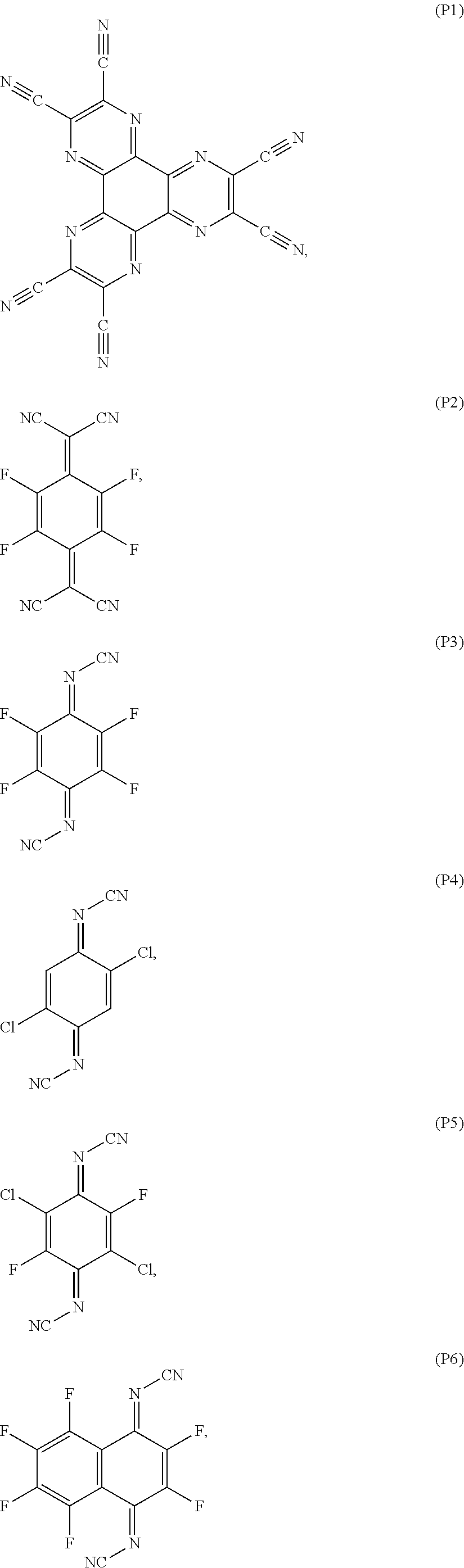
- the p-type dopant suitable for the ink composition may be selected from the group comprising:
- the p-type dopant of the ink composition may be preferably selected from the group comprising hexaazatriphenylene substituted with at least four nitrile groups.
- the p-type dopant of the ink composition may be preferably selected from the group comprising cyanobenzoquinone-dimethanes and/or cyanobenzoquinone-diimines, which are substituted with at least four electron withdrawing groups selected from the group comprising fluorine, chlorine, bromine and/or nitrile.
- the p-type dopant of the ink composition may be preferably selected from the group comprising radialene compounds, preferably [3]-radialene compounds, which are substituted with at least four electron withdrawing groups selected from the group comprising fluorine, chlorine, bromine and/or nitrile.
- the p-type dopant of the ink composition may be preferably selected from the group comprising tris(1-(pyridin-2-yl)-1H-pyrazol)cobalt(III) tris(hexafluorophosphate).
- the p-type dopant of the ink composition may be Molybdenum tris-[1,2-bis(trifluoromethyl)ethane-1,2-dithiolene].
- the p-type dopant of the ink composition may be a fluorinated fullerene, preferably C 60 F 48 .
- the p-type dopant of the ink composition may be preferably selected from the group comprising charge neutral metal amide compounds, which are substituted with at least four electron withdrawing groups selected from the group comprising fluorine, chlorine, bromine and/or nitrile.
- the p-type dopant of the ink composition may be preferably selected from the group comprising a metal organic complex, preferably a group Vb/VIb/VIIb metal organic complex, wherein at least one ligand is substituted with at least four electron withdrawing groups selected from the group comprising fluorine, chlorine, bromine and/or nitrile.
- the p-type dopant of the ink composition may be selected from the group of p-type dopants having the following chemical formula (P1) to (P25):
- M + is a monovalent cation, preferably an alkali cation.
- the organic charge transport materials may be small molecules or polymers or mixtures thereof.
- the organic charge transport material is a polymer or an oligomer.
- the polymer may be cross-linkable for instance in a way as described in WO2014037512.
- cross-linkable polymer HTM that may be suitable are described in Carlos A. Zuniga, Stephen Barlow, and Seth R. Marder, “Approaches to Solution-Processed Multilayer Organic Light-Emitting Diodes Based on Cross-Linking”, Chem. Mater. 2011, 23, 658-681, and incorporated by reference.
- the organic hole-transport material may be any compound that is commonly used to form an HTL and can be processed as a component of the ink composition.
- the ink composition comprises at least one organic charge transport material, wherein the amount of electron withdrawing groups in the sum formula of the at least one organic charge transport material is about ⁇ 0 and ⁇ 17 atomic percent and having a melting point of about ⁇ 100° C.
- An electron withdrawing group as defined according to the invention is fluorine, chlorine, bromine and/or nitrile.
- the ink composition comprises at least one organic charge transport material, wherein the amount of electron withdrawing groups in the sum formula of the at least one organic charge transport material is about ⁇ 0 atomic percent and about ⁇ 17 atomic percent and having a melting point of about ⁇ 100° C. to ⁇ 400° C.
- Polymer organic charge transport materials which are amorphous do not have a melting point.
- the electron withdrawing group of the at least one organic charge transport material of the ink composition is selected from fluorine, chlorine, bromine and/or nitrile; and preferably the electron withdrawing group is fluorine and/or nitrile.
- the ink composition may comprise at least two organic charge transport materials, of at least a first organic charge transport material and of at least a second organic charge transport material, wherein the molecular mass of the first organic charge transport material is lower than the molecular mass of the second organic charge transport material.
- the ink composition may comprise at least two organic charge transport materials, wherein
- An organic charge transport material in the sense of this invention may be compounds containing in their molecular structure formula at least one of the following molecular fragments as mentioned in Table 3 below.
- an organic charge transport material may comprise a spiro compound, a phthalocyanine compound, such as copper phthalocyanine (CuPc), a triphenyl amine compound like 4,4′,4′′-tris (3-methylphenylphenylamino) tri-phenylamine (m-MTDATA), TDATA, 2T-NATA, ⁇ -NPD (N,N′-Bis(naphthalen-1-yl)-N,N′-bis(phenyl)-benzidine), N4,N4,N4′′,N4′′-tetra([1,1′-biphenyl]-4-yl)-[1,1′:4′,1′′-terphenyl]-4,4′′-diamine, a spiro-compound like 2,2′,7,7′-tetrakis(N,N-di-p-methylphenylamino)-9,9′-spirobifluorene, a carbazole compound like tris(4-(4
- Additional organic charge transport material also named “HTL-materials” that can be suitable used are pentacene, dinaphthothienothiophene (DNTT), further DNTT derivatives such as C10-DNTT (in general Cx-DNTT), Metal-Phthalocyanines (ZnPc,CuPc), perylenes such as Diindenoperylenes (DIP), Tetrapropyl-tetraphenyl-diindenoperylene (P4-PH4-DIP), poly(3-hexylthiophen-2,5-diyl) (P3HT), DIPs-pentacene, poly[2,5-bis(3-alkylthiophen-2-yl)thieno(3,2-b)thiophene] (PBTTT) or n-type materials like poly ⁇ [N,N9-bis(2-octyldodecyl)-naphthalene-1,4,5,8-bis(dicarboximide
- HTL materials that can be further suitable used and are commercially available are 1,3-Bis(N-carbazolyl)benzene, 4,4′-Bis(N-carbazolyl)-1,1′-biphenyl, 4,4′-Bis(N-carbazolyl)-1,1′-biphenyl, 1,4-Bis(diphenylamino)benzene, 4,4′-Bis(3-ethyl-N-carbazolyl)-1,1′-biphenyl, N,N′-Bis(3-methylphenyl)-N,N′-diphenylbenzidine,N,N′-Bis(phenanthren-9-yl)-N,N′-bis(phenyl)-benzidine, Copper(II) phthalocyanine, Copper(II) phthalocyanine,4,4′-Cyclohexylidenebis[N,N-bis(4-methylphenyl)benzenamine],4-(Di
- Organic charge transport materials that may be used are Polymer-1, preferably (Poly[(9,9-di(2-ethylhex-1-yl)-9H-fluoren-2,7-diyl)-co-(4-4′-4′′-(4-azidobutox-1-yl)-N,N-diphenylaniline)]) and Polymer-2, preferably (Poly[(9,9-di(2-ethylhex-1-yl)-9H-fluoren-2,7-diyl)-co-(4-4′-4′′-(prop-2-yn-1-yloxy)-N,N-diphenylaniline)]), which may be cross-linked:
- the ink composition comprises at least one first auxiliary compound, wherein the first auxiliary compound is an aromatic nitrile compound, wherein the aromatic nitrile compound has about ⁇ 1 to about ⁇ 3 nitrile groups or has about ⁇ 1 to about ⁇ 2 nitrile groups, preferably 1 nitrile group, and a melting point of about ⁇ 100° C., wherein the first auxiliary compound is different from the p-type dopant.
- the first auxiliary compound is an aromatic nitrile compound, wherein the aromatic nitrile compound has about ⁇ 1 to about ⁇ 3 nitrile groups or has about ⁇ 1 to about ⁇ 2 nitrile groups, preferably 1 nitrile group, and a melting point of about ⁇ 100° C.
- the at least one first auxiliary compound may be selected from the group comprising substituted or unsubstituted benzonitrile.
- Substituted benzonitriles are preferably alkylbenzonitriles such as methylbenzonitrile, ortho-tolunitrile, and/or 4-butyl-benzonitrile.
- the at least one first auxiliary compound may be selected from the group comprising substituted or unsubstituted benzonitrile compounds, wherein the substituents may be selected from alkyl, hetero or non-hetero cycloalkyl, hetero or non-hetero aryl, and/or halogen.
- the first auxiliary compound may be selected from 3-Acetylbenzonitrile, 4-Acetylbenzonitrile, Benzonitrile, Benzoylacetonitrile, 4-Butylbenzonitrile, 4-tert-Butylbenzonitrile, 4-Cyanophenylacetonitrile, 2,3-Dimethoxybenzonitrile, 3,4-Dimethoxybenzonitrile, 2-Ethylbenzonitrile, 3-Ethylbenzonitrile, 4-Ethylbenzonitrile 2-Methoxybenzonitrile, 3-Methoxybenzonitrile, 4-Methoxybenzonitrile, 4-Methoxybenzoylacetonitrile, 4-(Methoxymethyl)benzonitrile, Phenylacetonitrile, 2-Phenylbutyronitrile, 3-Phenylpropionitrile, 2-Propylenebenzonitrile, 4-Propylbenzonitrile o-Tolunitrile, m-Tolunitrile, p-Tol
- alkyl group refers to a saturated aliphatic hydrocarbyl group.
- the alkyl group may be a C 1 to C 10 alkyl group. More specifically, the alkyl group may be a C 1 to C 10 alkyl group or a C 1 to C 6 alkyl group.
- a C 1 to C 4 alkyl group includes 1 to 4 carbons in alkyl chain, and may be selected from methyl, ethyl, propyl, iso-propyl, n-butyl, iso-butyl, sec-butyl, and t-butyl.
- alkyl group may be a methyl group, an ethyl group, a propyl group, an isopropyl group, a butyl group, an isobutyl group, a t-butyl group, a pentyl group, a hexyl group.
- aryl group refers to a hydrocarbyl group which can be created by formal abstraction of one hydrogen atom from an aromatic ring in the corresponding aromatic hydrocarbon.
- Aromatic hydrocarbon refers to a hydrocarbon which contains at least one aromatic ring or aromatic ring system.
- Aromatic ring or aromatic ring system refers to a planar ring or ring system of covalently bound carbon atoms, wherein the planar ring or ring system comprises a conjugated system of delocalized electrons fulfilling Hückel's rule.
- aryl groups include monocyclic groups like phenyl or tolyl, polycyclic groups which comprise more aromatic rings linked by single bonds, like biphenylyl, and polycyclic groups comprising fused rings, like naphtyl or fluoren-2-yl.
- heteroaryl it is understood a group derived by formal abstraction of one ring hydrogen from a heterocyclic aromatic ring in a compound comprising at least one such ring.
- hetero or non-hetero cycloalkyl it is understood a group derived by formal abstraction of one ring hydrogen from a hetero or non-hetero cyclic ring having from 3 to 12 ring atoms.
- hetero is understood the way that at least one carbon atom, in a structure which may be formed by covalently bound carbon atoms, is replaced by another polyvalent atom.
- the hetero atoms are selected from B, Si, N, P, O, S; more preferably from N, P, O, S.
- Halogen stand for halogens selected from the group comprising F, Cl, Br and I, wherein F and Cl are more preferred.
- the molecular mass of the at least one first auxiliary compound can be in the range of about ⁇ 100 g/mol to about ⁇ 500 g/mol, preferably about ⁇ 100 g/mol to about ⁇ 400 g/mol, more preferred about ⁇ 100 g/mol to about ⁇ 300 g/mol.
- the ink composition comprises at least one second auxiliary compound, wherein the second auxiliary compound is liquid at about 23° C., and wherein the at least one second auxiliary compound has a chemical structure that is different from the first auxiliary compound and is different from the p-type dopant, preferably the second auxiliary compound is free of a nitrile group and/or is free of an electron withdrawing group.
- the second auxiliary compound may be selected from the group comprising:
- the use of the second auxiliary compound may be advantageous for the ink properties, for the printing properties of the ink and for the drying behavior, film formation and homogeneity of the printed film.
- the second auxiliary compound has a boiling point at atmospheric pressure which is larger than 50° C., preferrably the boiling point of the second auxiliary compound is between 50° C. and 350° C., more preferably between 100° C. and 350° C., more preferred between 150° C. and 350° C.
- the ink composition according to a preferred embodiment may be free of water.
- the ink composition can comprise water in the range from about ⁇ 0 wt.-% to about ⁇ 5 wt.-%, preferably about ⁇ 0 wt.-% to about ⁇ 1 wt.-%, more preferred about ⁇ 0 wt.-% to about ⁇ 0.1 wt.-% and in addition preferred about ⁇ 0 wt.-% to about ⁇ 0.01 wt.-%; wherein the wt.-% is based on the total weight amount of the ink composition.
- the content of water may destabilize the ink composition.
- an ink composition that does not contain water may be a preferred embodiment.
- the ink composition may have at least one of the following physical data
- the ink composition may be liquid at a temperature in the range of about 10° C. to 150° C., preferably in the range of about 20° C. to 100° C., further preferred in the range of about 23° C. to 80° C.
- the ink composition may be a solution in the range of about ⁇ 0° C. to about ⁇ 100° C., preferably in the range of about ⁇ 15° C. to about ⁇ 50° C., further preferred in the range of about ⁇ 20° C. to about ⁇ 30° C., and in addition preferred in the range of about ⁇ 21° C. to about ⁇ 23° C.
- the ink composition may have a boiling point of about ⁇ 50° C. to about ⁇ 350° C., preferably of about ⁇ 80° C. to about ⁇ 320° C. and further preferred of about ⁇ 100° C. to about ⁇ 300° C. and in addition preferred ⁇ 150° C. to about ⁇ 250° C.
- the ink composition may have a surface tension at about 23° C. in the range from about ⁇ 15 dyn/cm to about ⁇ 50 dyn/cm, preferably about ⁇ 20 dyn/cm to about ⁇ 40 dyn/cm.
- the ink composition may have a surface tension at about 50° C. in the range from about ⁇ 15 dyn/cm to about ⁇ 50 dyn/cm, preferably about ⁇ 20 dyn/cm to about ⁇ 40 dyn/cm.
- the surface tension may be adjusted to low values by the addition of a second auxiliary compound in order to achieve good wetting of the ink on a substrate.
- the second auxiliary compound may be a fluorinated hydrocarbon compound.
- the ink composition may be a homogeneous solution at about 20° C.
- the ink composition may be a homogeneous solution at about 23° C.
- the ink composition may be a homogeneous solution at about 30° C.
- the ink composition may be a homogeneous solution at about 50° C.
- FIG. 2 shows the UV-vis absorption spectrum (350 nm to 800 nm wavelength) at t 0 in different solvents of the [3]-radialene compound P11, 4,4′,4′′-((1E,1′E,1′′E)-cyclopropane-1,2,3-triylidenetris(cyanomethanylylidene))tris(2,3,5,6-tetrafluorobenzonitrile);
- FIG. 3 shows the UV-vis absorption spectrum (350 nm to 800 nm wavelength) at t 0 in different solvents of the [3]-radialene of compound P15, 2,2′,2′′-(cyclopropane-1,2,3-triylidene)tris(2-(2,3,5,6-tetrafluoro-4-(trifluoromethyl)phenyl)-acetonitrile);
- FIG. 4 shows the UV-vis absorption spectrum (350 nm to 800 nm wavelength) at t 0 in different solvents of the [3]-radialene compound P18, (2E,2′E,2′′E)-2,2′,2′′-(cyclopropane-1,2,3-triylidene)tris(2-(2,3,5-trifluoro-4,6-bis(trifluoromethyl)phenyl)acetonitrile);
- FIG. 6 shows the UV-vis absorption spectrum (350 nm to 800 nm wavelength) after 1 week in different solvents of Molybdenum tris-[1,2-bis(trifluoromethyl)ethane-1,2-dithiolene] (Mo(tfd) 3 ) of compound P20;
- FIG. 7 shows the UV-vis absorption spectrum (350 nm to 800 nm wavelength) after 1 week in different solvents of the [3]-radialene of compound P11, 4,4′,4′′-((1E,1′E,1′′E)-cyclopropane-1,2,3-triylidenetris(cyanomethanylylidene))tris(2,3,5,6-tetrafluorobenzonitrile);
- FIG. 8 shows the UV-vis absorption spectrum (350 nm to 800 nm wavelength) after 1 week in different solvents of the [3]-radialene compound P15, 2,2′,2′′-(cyclopropane-1,2,3-triylidene)tris(2-(2,3,5,6-tetrafluoro-4-(trifluoromethyl)phenyl)-acetonitrile);
- FIG. 9 shows the UV-vis absorption spectrum (350 nm to 800 nm wavelength) after 1 week in different solvents of the [3]-radialene compound P18, (2E,2′E,2′′E)-2,2′,2′′-(cyclopropane-1,2,3-triylidene)tris(2-(2,3,5-trifluoro-4,6-bis(trifluoromethyl)phenyl)acetonitrile);
- FIG. 10 shows the UV-vis absorption spectrum (350 nm to 800 nm wavelength) with respect to the absorption intensity of [3]-radialene compound P17 in different nitrile-free solvents, comparative examples 5a to 5e, for a time period from to to 22 h ink storage;
- FIG. 11 shows the UV-vis absorption spectrum (350 nm to 800 nm wavelength) with respect to the absorption intensity of the [3]-radialene compound P17 in different nitrile solvents (inventive examples 6a an 6b) for a time period from t 0 to 22 h ink storage time;
- FIG. 12 shows the UV-vis absorption spectrum (350 nm to 800 nm wavelength) with respect to the absorption intensity of compound P8 in toluene (comparative example 7) at t 0 and t 7d (7 days ink storage time);
- FIG. 13 shows the UV-vis absorption spectrum (350 nm to 800 nm wavelength) with respect to the absorption intensity of compound P8 in anisole (comparative example 8) at t 0 and t 7d (7 days ink storage time);
- FIG. 14 shows the UV-vis absorption spectrum (350 nm to 800 nm wavelength) with respect to the absorption intensity of the inventive example compound P8 in benzonitrile (inventive example 9) at t 0 and t 7d (7 days ink storage time);
- FIG. 16 shows the absorption intensity in an UV-vis absorption spectrum (350 nm to 800 nm wavelength) for the organic charge transport material of polymer-1 in benzonitrile for a time period starts at t 0 to t 17h (17 h);
- FIG. 17 shows the intensity of the UV-vis absorption maximum at 580 nm of Molybdenum tris-[1,2-bis(trifluoromethyl) ethane-1,2-dithiolene] (Mo(tfd) 3 ) [compound P20] dissolved in acetonitril and isovaleronitril;
- FIG. 1 shows the UV-vis absorption spectrum (350 nm to 800 nm wavelength) at t 0 of Molybdenum tris-[1,2-bis(trifluoromethyl)ethane-1,2-dithiolene] (Mo(tfd) 3 ) of the p-type dopant compound P20:
- aromatic nitrile solution which is benzonitrile
- aromatic nitrile-free solutions which are toluene and anisole
- FIG. 2 shows the UV-vis absorption spectrum (350 nm to 800 nm wavelength) at t 0 of the p-type dopant compound P11:
- aromatic nitrile solution which is benzonitrile
- aromatic nitrile-free solutions which are toluene and anisole
- FIG. 4 shows the UV-vis absorption spectrum (350 nm to 800 nm wavelength) at t 0 of the p-type dopant compound P18:
- FIG. 5 shows the UV-vis absorption spectrum (350 nm to 800 nm wavelength) at t 0 of the p-type dopant fullerene compound C 60 F 48 (P21), in an aromatic nitrile solution, which is benzonitrile, and in aromatic nitrile-free solutions, which are toluene and anisole.
- FIG. 6 shows the UV-vis absorption spectrum (350 nm to 800 nm wavelength) at t 0 and t 7d (1 week ink storage) for the p-type dopant compound P20:
- FIG. 7 shows the UV-vis absorption spectrum (350 nm to 800 nm wavelength) at t 0 and t 7d (1 week ink storage) for the p-type dopant compound P11:
- FIG. 8 shows the UV-vis absorption spectrum (350 nm to 800 nm wavelength) at t 0 and t 7d (1 week ink storage) for the p-type dopant compound P15:
- FIG. 9 shows the UV-vis absorption spectrum (350 nm to 800 nm wavelength) at t 0 and t 7d (1 week ink storage) for the p-type dopant compound P18:
- FIG. 10 shows the UV-vis absorption spectrum (350 nm to 800 nm wavelength) with respect to the absorption intensity of [3]-radialene p-type dopant compound P17 comparative examples 5a to 5e in different nitrile-free solvents, comparative examples 5a to 5e, for a time period at from t0 for to 22 h ink storage. It is evident that the absorption intensity decreases over time. The decrease of intensity is caused by a reduction of the amount of absorbing compound P17 in the solution. The reduction of the amount of absorbing compound P17 in the solution is attributed to a decomposition of P17 in the solution.
- FIG. 11 shows the UV-vis absorption spectrum (350 nm to 800 nm wavelength) with respect to the absorption intensity of [3]-radialene p-type dopant compound P17 in different nitrile solvents, inventive examples 6a and 6b, for a time period at from t0 for to 22 h ink storage. It is evident that the absorption intensity remains constant at high level (>97%) over time (6a) or increases (6b). Constant absorption intensity (6a) is attributed to constant amount of absorbing compound P17 in the solution over time. P17 is stable in the solution. Increasing absorption intensity (6b) is attributed to increasing amount of absorbing compound P17 in the solution over time. This is indicative of a slow dissolution of P17. After about 17 hours the absorption intensity reaches a constant and high (>97%) level. P17 is stable in the solution.
- FIG. 12 shows the absorption intensity in an UV-vis absorption spectrum (350 nm to 800 nm wavelength) for the p-type dopant compound P8:
- FIG. 13 shows the absorption intensity in an UV-vis absorption spectrum (350 nm to 800 nm wavelength) for the p-type dopant compound P8:
- FIG. 14 shows the absorption intensity in an UV-vis absorption spectrum (350 nm to 800 nm wavelength) for the p-type dopant compound P8:
- FIG. 15 shows the absorption intensity in an UV-vis absorption spectrum (350 nm to 800 nm wavelength) for the organic charge transport material of polymer-1:
- anisole for a time period starts at t 0 to t 17h (17 h).
- FIG. 16 shows the absorption intensity in an UV-vis absorption spectrum (350 nm to 800 nm wavelength) for the organic charge transport material of polymer-1:
- FIG. 16 shows that the loss in absorption of the solution of polymer-1 in anisole after 17 h storage at 23° C. is 3%.
- FIG. 16 shows that the loss in absorption of the solution of polymer-1 in benzonitrile after 17 h storage at 23° C. is below the resolution limit of the measurement technique which is 0.8%.
- FIGS. 17 and 18 clearly demonstrate that a p-type dopant, such as Molybdenum tris-[1,2-bis(trifluoromethyl) ethane-1,2-dithiolene] (Mo(tfd) 3 ) [compound P20], is not stable in a non-aromatic nitrile solution, such as acetonitrile solution or isovaleronitrile solution, compared with an aromatic nitrile solution—see FIG. 6 and FIG. 11 .
- a p-type dopant such as Molybdenum tris-[1,2-bis(trifluoromethyl) ethane-1,2-dithiolene] (Mo(tfd) 3 ) [compound P20]
- FIGS. 15 and 16 clearly demonstrate that an organic charge transport material can be stabilized in an aromatic nitrile solution for storage significant better than in a nitrile-free solvent—see FIG. 10 or in a non-aromatic nitrile solution—see FIGS. 17 and 18 .
- the deposition method may be a printing method like ink jet printing, screen printing, offset printing, flexographic printing, spin coating, slot-die coating, spray coating, Langmuir-Blodgett (LB)method.
- LB Langmuir-Blodgett
- It may be a coating method like spin coating, slot-die coating, spray coating, or an imprinting method like nano-imprinting.
- the ink composition may be processed by solution-processing, preferably by spin coating, slot die coating and/or inkjet printing.
- the organic semiconductor layer obtained from the ink composition is arranged in direct contact with an anode.
- the organic layers that can be obtained by using the ink composition according to the invention, for example by means of a solution processing, may have a layer thickness in the range of about ⁇ 1 nm to about ⁇ 1 ⁇ m, preferably of about ⁇ 2 nm to about ⁇ 500 nm, and further preferred of about ⁇ 5 nm to about ⁇ 200 nm.
- the organic layers manufactured by the ink composition may have a conductivity sigma of about 1E-7 S/cm ⁇ sigma ⁇ 1E1 S/cm.
- the organic layers obtained by using the ink composition according to the invention may be used in an electronic device as follows:
- a standard OLED was used to test the inventive ink composition.
- the layers comprising the inventive OLED devices Inv-OLED-1 to Inv-OLED-4 were deposited sequentially as follows:
- the layer was dried on a hot plate at 60° C. for 1 min and subsequently a hard bake for cross-linking was applied for 30 mins at 150° C.
- VTE vacuum thermal evaporation
- All subsequent layers were deposited by vacuum thermal evaporation (VTE) at a pressure of about 1E-7 mbar and a deposition rate of about 1 Angstrom per second for the organic layers and about 3 Angstrom per second for the aluminium cathode layer.
- Inv-OLED-1 to Inv-OLED-4 a liquid ink composition, liquid at 23° C., was obtained by mixing the components:
- the total solid content in the ink was 2 wt.-%, based on the total weight amount of the ink composition.
- the content of p-type dopant P17 in the solid HIL-layer is 20 wt %, obtained after the benzonitrile and anisole was removed, and calculated on the total weight amount of the solid HIL-layer.
- the ratio between Polymer-1 and Polymer-2 is 3.6:10 by weight.
- the device performance data of the OLEDs comprising a HIL-layer prepared with the inventive ink according to examples Inv-OLED-1 to Inv-OLED-4 are shown in table 5.
Abstract
Description

in which W, X, Y and Z independently represent hydrogen, halogen, hydroxyl group, hydrocarbon group having 1 to 8 carbon atoms, alkoxy group or acyloxy group provided that W═Y and X═Z, or W═Z and X═Y. The compositions and charge transfer complexes comprising these compounds are also described together with intermediates for the compounds.
-
- at least one p-type dopant comprising electron withdrawing groups;
- at least one first auxiliary compound, wherein the first auxiliary compound is an aromatic nitrile compound, wherein the aromatic nitrile compound has about ≥1 to about ≤3 nitrile groups and a melting point of about <100° C., wherein the first auxiliary compound is different from the p-type dopant; and
wherein the electron withdrawing groups are fluorine, chlorine, bromine and/or nitrile.
-
- at least one p-type dopant comprising electron withdrawing groups;
- at least one organic charge transport material, wherein the organic charge transport material is different from the p-type dopant;
- at least one first auxiliary compound, wherein the first auxiliary compound is an aromatic nitrile compound, wherein the aromatic nitrile compound has about ≥1 to about ≤3 nitrile groups and a melting point of about <100° C., wherein the first auxiliary compound is different from the p-type dopant; and
wherein the electron withdrawing groups are fluorine, chlorine, bromine and/or nitrile.
-
- at least one p-type dopant comprising electron withdrawing groups;
- at least one first auxiliary compound, wherein the first auxiliary compound is an aromatic nitrile compound, wherein the aromatic nitrile compound has about ≥1 to about ≤3 nitrile groups and a melting point of about <100° C., wherein the first auxiliary compound is different from the p-type dopant; and
wherein the electron withdrawing groups are fluorine, chlorine, bromine and/or nitrile; and - for 10 g solid of a p-type dopant of compound P11 [4,4′,4″-((1E,1′E,1″E)-cyclopropane-1,2,3-triylidenetris(cyanomethanylylidene))tris(2,3,5,6-tetrafluorobenzonitrile)] (NDP-9, available from NovaLED)] dissolved per 1 ml benzonitrile, the ink composition may comprises in addition at least one second auxiliary compound, which is liquid at about 23° C., and wherein the at least one second auxiliary compound has a chemical structure that is different from the first auxiliary compound and is different from the p-type dopant.
-
- at least one p-type dopant comprising electron withdrawing groups;
- at least one first auxiliary compound, wherein the first auxiliary compound is an aromatic nitrile compound, wherein the aromatic nitrile compound has about ≥1 to about ≤3 nitrile groups and a melting point of about <100° C., wherein the first auxiliary compound is different from the p-type dopant; and
wherein the electron withdrawing groups are fluorine, chlorine, bromine and/or nitrile; and - for a p-type dopant of compound P11 [4,4′,4″-((1E,1′E,1″E)-cyclopropane-1,2,3-triylidenetris(cyanomethanylylidene))tris(2,3,5,6-tetrafluorobenzonitrile)] (NDP-9, available from NovaLED)] dissolved in benzonitrile, the ink composition may comprises in addition at least one second auxiliary compound, which is liquid at about 23° C., and wherein the at least one second auxiliary compound has a chemical structure that is different from the first auxiliary compound and is different from the p-type dopant.
-
- at least one p-type dopant comprising electron withdrawing groups;
- at least one first auxiliary compound, wherein the first auxiliary compound is an aromatic nitrile compound, wherein the aromatic nitrile compound has about ≥1 to about ≤3 nitrile groups and a melting point of about <100° C., wherein the first auxiliary compound is different from the p-type dopant; and
wherein the electron withdrawing groups are fluorine, chlorine, bromine and/or nitrile;
wherein the ink composition comprises in addition at least one second auxiliary compound, which is liquid at about 23° C., and wherein the at least one second auxiliary compound has a chemical structure that is different from the first auxiliary compound and is different from the p-type dopant.
-
- at least one p-type dopant comprising electron withdrawing groups;
- at least one first auxiliary compound, wherein the first auxiliary compound is an aromatic nitrile compound, wherein the aromatic nitrile compound has about ≥1 to about ≤3 nitrile groups and a melting point of about <100° C., wherein the first auxiliary compound is different from the p-type dopant; and
wherein the electron withdrawing groups are fluorine, chlorine, bromine and/or nitrile;
wherein the ink composition comprises in addition at least one second auxiliary compound, which is liquid at about 23° C., and wherein the at least one second auxiliary compound has a chemical structure that is different from the first auxiliary compound and is different from the p-type dopant; and
wherein the second auxiliary compound has a boiling point at atmospheric pressure which is ≥50° C., preferrably the boiling point of the second auxiliary compound is between ≥50° C. and ≤350° C., more preferably between ≥100° C. and ≤350° C., more preferred between ≥150° C. and ≤350° C.
-
- at least one p-type dopant comprising electron withdrawing groups, and which is solid at about ≥100° C.;
- at least one organic charge transport material, which is solid at about ≥100° C., and wherein the organic charge transport material is different from the p-type dopant;
- at least one first auxiliary compound, wherein the first auxiliary compound is an aromatic nitrile compound, wherein the aromatic nitrile compound has about ≥1 to about ≤3 nitrile groups and a melting point of about <100° C., wherein the first auxiliary compound is different from the p-type dopant; and
wherein the electron withdrawing groups are fluorine, chlorine, bromine and/or nitrile.
-
- i) —at least one p-type dopant comprising electron withdrawing groups;
- at least one first auxiliary compound, wherein the first auxiliary compound is an aromatic nitrile compound, wherein the aromatic nitrile compound has about ≥1 to about ≤3 nitrile groups and a melting point of about <100° C., wherein the first auxiliary compound is different from the p-type dopant; and
- wherein the electron withdrawing groups are fluorine, chlorine, bromine and/or nitrile;
- wherein the ink composition comprises in addition at least one second auxiliary compound, which is liquid at about 23° C., and wherein the at least one second auxiliary compound has a chemical structure that is different from the first auxiliary compound and is different from the p-type dopant, preferably the second auxiliary compound is free of a nitrile group and/or is free of an electron withdrawing group; or
- ii) —at least one p-type dopant comprising electron withdrawing groups, and which is solid at about ≥100° C.;
- at least one organic charge transport material, which is solid at about ≥100° C., and wherein the organic charge transport material is different from the p-type dopant;
- at least one first auxiliary compound, wherein the first auxiliary compound is an aromatic nitrile compound, wherein the aromatic nitrile compound has about ≥1 to about ≤3 nitrile groups and a melting point of about <100° C., wherein the first auxiliary compound is different from the p-type dopant; and
- wherein the electron withdrawing groups are fluorine, chlorine, bromine and/or nitrile.
- i) —at least one p-type dopant comprising electron withdrawing groups;
-
- at least one p-type dopant comprising electron withdrawing groups, and which is solid at about ≥100° C.;
- at least one organic charge transport material, which is solid at about ≥100° C., and wherein the organic charge transport material is different from the p-type dopant;
- at least one first auxiliary compound, wherein the first auxiliary compound is an aromatic nitrile compound, wherein the aromatic nitrile compound has about ≥1 to about ≤3 nitrile groups and a melting point of about <100° C., wherein the first auxiliary compound is different from the p-type dopant; and
wherein the electron withdrawing groups are fluorine, chlorine, bromine and/or nitrile.
-
- at least one p-type dopant, wherein the amount of electron withdrawing groups in the sum formula of the at least one p-type dopant is about ≥17 atomic percent to about ≤90 atomic percent;
- at least one organic charge transport material, wherein the amount of electron withdrawing groups in the sum formula of the at least one organic charge transport material is ≥0 to about <17 atomic percent, and wherein the organic charge transport material is different from the p-type dopant;
- at least one first auxiliary compound, wherein the first auxiliary compound is an aromatic nitrile compound, wherein the aromatic nitrile compound has about ≥1 to about ≤3 nitrile groups and a melting point of about <100° C., wherein the first auxiliary compound is different from the p-type dopant; and
wherein the electron withdrawing groups are fluorine, chlorine, bromine and/or nitrile.
-
- at least one p-type dopant, comprises at least about ≥3 electron withdrawing groups;
- at least one organic charge transport material comprises at least about 0 to about <3 electron withdrawing groups, and wherein the organic charge transport material is different from the p-type dopant;
- at least one first auxiliary compound, wherein the first auxiliary compound is an aromatic nitrile compound, wherein the aromatic nitrile compound has about ≥1 to about ≤3 nitrile groups and a melting point of about <100° C., wherein the first auxiliary compound is different from the p-type dopant; and
wherein the electron withdrawing groups are fluorine, chlorine, bromine and/or nitrile.
-
- at least one p-type dopant, having about ≥4 atoms and wherein the amount of electron withdrawing groups in the sum formula of the at least one p-type dopant is about ≥17 atomic percent to about ≤90 atomic percent;
- at least one organic charge transport material, having about ≥4 atoms and wherein the amount of electron withdrawing groups in the sum formula of the at least one organic charge transport material is ≥0 to about <17 atomic percent, wherein the organic charge transport material is different from the p-type dopant and the first auxiliary compound;
- at least one first auxiliary compound, wherein the first auxiliary compound is an aromatic nitrile compound, wherein the aromatic nitrile compound has about ≥1 to about ≤3 nitrile groups and a melting point of about <100° C., wherein the first auxiliary compound is different from the p-type dopant and the organic charge transport material; and wherein the electron withdrawing groups are fluorine, chlorine, bromine and/or nitrile.
-
- at least one p-type dopant, having about ≥4 atoms and wherein the amount of electron withdrawing groups in the sum formula of the at least one p-type dopant is about ≥17 atomic percent to about ≤90 atomic percent;
- at least one organic charge transport material, having about ≥4 atoms and wherein the amount of electron withdrawing groups in the sum formula of the at least one organic charge transport material is ≥0 to about <17 atomic percent and having a melting point of about ≥100° C.;
- at least one first auxiliary compound, wherein the first auxiliary compound is an aromatic nitrile compound, wherein the aromatic nitrile compound has about ≥1 to about ≤3 nitrile groups and a melting point of about <100° C., wherein the first auxiliary compound is different from the p-type dopant; and
wherein the electron withdrawing groups are fluorine, chlorine, bromine and/or nitrile.
-
- at least one p-type dopant, having about ≥4 atoms and wherein the amount of electron withdrawing groups in the sum formula of the at least one p-type dopant is about ≥22 atomic percent to about ≤90 atomic percent;
- at least one organic charge transport material, having about ≥6 atoms, preferably about ≥12 atoms, and wherein the amount of electron withdrawing groups in the sum formula of the at least one organic charge transport material is ≥0 to about <17 atomic percent and having a melting point of about ≥100° C.;
- at least one first auxiliary compound, wherein the first auxiliary compound is an aromatic nitrile compound, wherein the aromatic nitrile compound has about ≥1 to about ≤3 nitrile groups and a melting point of about <100° C., wherein the first auxiliary compound is different from the p-type dopant; and
wherein the electron withdrawing groups are fluorine, chlorine, bromine and/or nitrile.
-
- at least one p-type dopant, having about ≥4 atoms and wherein p-type dopant comprises at least about ≥3 electron withdrawing groups and about ≤100 electron withdrawing groups;
- at least one organic charge transport material, having about ≥4 atoms and wherein the organic charge transport material has ≥0 to <3 electron withdrawing groups and a melting point of about ≥100° C.;
- at least one first auxiliary compound, wherein the first auxiliary compound is an aromatic nitrile compound, wherein the aromatic nitrile compound has about ≥1 to about ≤3 nitrile groups and a melting point of about <100° C., wherein the first auxiliary compound is different from the p-type dopant; and
wherein the electron withdrawing groups are fluorine, chlorine, bromine and/or nitrile.
-
- at least one p-type dopant, having about ≥4 atoms and wherein the amount of electron withdrawing groups in the sum formula of the at least one p-type dopant is about ≥22 atomic percent to about ≤90 atomic percent;
- at least one organic charge transport material, having about ≥6 atoms, preferably about ≥12 atoms, and wherein the amount of electron withdrawing groups in the sum formula of the at least one organic charge transport material is ≥0 to about <17 atomic percent and having a melting point of about ≥100° C.;
- at least one first auxiliary compound, wherein the first auxiliary compound is an aromatic nitrile compound, wherein the aromatic nitrile compound has about ≥1 to about ≤2 nitrile groups and a melting point of about <100° C., wherein the first auxiliary compound is different from the p-type dopant; and
wherein the electron withdrawing groups are fluorine, chlorine, bromine and/or nitrile.
-
- at least one p-type dopant, having about ≥4 atoms and wherein p-type dopant comprises at least about ≥3 electron withdrawing groups and about ≤100 electron withdrawing groups;
- at least one organic charge transport material, having about ≥4 atoms and wherein the organic charge transport material has ≥0 to <3 electron withdrawing groups and a melting point of about ≥100° C.;
- at least one first auxiliary compound, wherein the first auxiliary compound is an aromatic nitrile compound, wherein the aromatic nitrile compound has about ≥1 to about ≤2 nitrile groups and a melting point of about <100° C., wherein the first auxiliary compound is different from the p-type dopant; and
wherein the electron withdrawing groups are fluorine, chlorine, bromine and/or nitrile.
| TABLE 1 | ||||
| Total number of atoms | Number of electron | Atomic % of electron | ||
| Simplified sum formula | and electron withdrawing | withdrawing groups | withdrawing groups in | |
| (electron withdrawing | groups in the simplified | in the simplified | p-type dopant (at % | |
| Compound Name | groups in brackets) | sum formula [A] | sum formula [B] | EWG = [B] * 100%/[A] |
| N4,N4″-bis(3,5- | C54H32N2(F)12 | 100 | 12 | 100% × 12/100 = 12% |
| bis(trifluoromethyl) | ||||
| phenyl)-N4,N4″- | ||||
| di(naphthalen-2-yl)- | ||||
| [1,1′:4′,1″-terphenyl]- | ||||
| 4,4″-diamine (example | ||||
| for organic charge | ||||
| transport material) | ||||
| TABLE 2 | ||||
| Simplified sum | Total number of atoms | Number of electron | Atomic % of electron | |
| formula (electron | and electron withdrawing | withdrawing groups | withdrawing groups in | |
| withdrawing groups | groups in the simplified | in the simplified | p-type dopant (at % | |
| P-type Dopant | in brackets) | sum formula [A] | sum formula [B] | EWG = [B] * 100%/[A] |
| P1 | C12N6(CN)6 | 24 | 6 | 25.00 |
| P2 | C8(F)4(CN)4 | 16 | 8 | 50.00 |
| P3 | C6N2(F)4(CN)2 | 14 | 6 | 42.86 |
| P4 | C6N2(Cl)2(CN)2 | 12 | 4 | 33.33 |
| P5 | C6N2(F)2(Cl)2(CN)2 | 14 | 6 | 42.86 |
| P6 | C10N2(F)6(CN)2 | 20 | 8 | 40.00 |
| P7 | C10O2S4(CN)4 | 20 | 4 | 20.00 |
| P8 | C12(F)6(CN)4 | 22 | 10 | 45.45 |
| P9 | C8(F)2(Br)2(CN)4 | 16 | 8 | 50.00 |
| P10 | C20(F)10(CN)6 | 36 | 16 | 44.44 |
| P11 | C24(F)12(CN)6 | 42 | 18 | 42.86 |
| P12 | C27(F)15(Cl)6(CN)3 | 51 | 24 | 47.06 |
| P13 | C24(F)15(CN)3 | 42 | 18 | 42.86 |
| P14 | C42(F)27(CN)3 | 72 | 30 | 41.67 |
| P15 | C27(F)21(CN)3 | 51 | 24 | 47.06 |
| P16 | C21N3(F)12(CN)3 | 39 | 15 | 38.46 |
| P17 | C24(F)9(CN)6 | 39 | 15 | 38.46 |
| P18 | C30(F)27(CN)3 | 60 | 30 | 50.00 |
| P19 | C24H27CoN9P3(F)18 | 82 | 18 | 21.95 |
| P20 | C12MoS6(F)18 | 37 | 18 | 48.65 |
| P21 | C60(F)48 | 108 | 48 | 44.44 |
| P22 | C15N12(CN)6 | 33 | 6 | 18.18 |
| P23 | C24O4N2(F)16 | 46 | 16 | 34.78 |
| P24 | C14N6(F)12(CN)2 | 34 | 14 | 41.18 |
| P25 | C24BM(F)20 | 46 | 20 | 43.48 |
P-Type Dopant
-
- hexaazatriphenylene substituted with at least four nitrile groups;
- cyanobenzoquinone-dimethanes and/or cyanobenzoquinone-diimines, which are substituted with at least four electron withdrawing groups selected from the group comprising fluorine, chlorine, bromine and/or nitrile;
- radialene compounds, preferably [3]-radialene compounds, which are substituted with at least four electron withdrawing groups selected from the group comprising fluorine, chlorine, bromine and/or nitrile;
- tris(1-(pyridin-2-yl)-1H-pyrazol)cobalt(III) tris(hexafluorophosphate);
- Molybdenum tris-[1,2-bis(trifluoromethyl)ethane-1,2-dithiolene];
- C60F48;
- charge neutral metal amide compounds, which are substituted with at least four electron withdrawing groups selected from the group comprising fluorine, chlorine, bromine and/or nitrile;
- metal organic complex, preferably a group Vb/VIb/VIIb metal organic complex, wherein at least one ligand is substituted with at least four electron withdrawing groups selected from the group comprising fluorine, chlorine, bromine and/or nitrile.


wherein M+ is a monovalent cation, preferably an alkali cation.
Organic Charge Transport Material
-
- the average molecular mass of the first organic charge transport material is in the range of about ≥300 g/mol to about ≤1500 g/mol, preferably about ≥400 g/mol to about ≤1300 g/mol; and/or
- the average molecular mass of the second organic charge transport material is in the range of ≥600 g/mol to about ≤2,000,000, preferably about ≥1000 g/mol to about ≤1,000,000 g/mol, more preferred about ≥1000 g/mol to about ≤500,000 g/mol;
wherein the molecular mass of the first organic charge transport material is lower than the molecular mass of the second organic charge transport material.
| TABLE 3 |
| Typical molecular fragments of organic charge transport materials |
| Molecular Fragment | Fragment Name |
 |
Triarylamine |
 |
Carbazole |
 |
Benzo[5,6][1,4]oxa- thiino[2,3-b]pheno- xathiine |
 |
Phenothiazine |
 |
Phosphanimine |
 |
Imidazolethione |
 |
Imidazolone |
 |
Phenylimidazolidine imine |
|
|
Pentacene |
 |
Fluorene |
|
|
Thiophene |
-
- carbazole compounds, such as N-phenylcarbazole or polyvinylcarbazole;
- amine compounds having an aromatic condensation ring, such as N,N′-bis(3-methylphenyl)-N,N′-diphenyl-[1,1-biphenyl]-4,4′-diamine (TPD), or N,N′-di(naphthalen-1-yl)-N,N′-diphenyl benzydine (alpha-NPD);
- triphenylamine compounds, such as 4,4′,4″-tris(N-carbazolyl)triphenylamine (TCTA) or N4,N4″-bis(3,5-bis(trifluoromethyl)phenyl)-N4,N4″-di(naphthalen-2-yl)-[1,1′:4′,1″-terphenyl]-4,4″-diamine, or thiophene-based compounds, such as poly(3-hexylthiophene)-2,5-diyl.

First Auxiliary Compound
-
- an alkane compound, such as nonane, decane, undecane, or dodecane;
- an aliphatic alcohol compound, such as hexanol, heptanol, octanol, nonyl alcohol, or decyl alcohol;
- an aliphatic ether compound, such as dibutyl ether, dipentyl ether, diethylene glycol dimethyl ether, diethylene glycol ethyl methyl ether, diethylene glycol isopropyl methyl ether, diethylene glycol diethyl ether, diethylene glycol butyl methyl ether, diethylene glycol dibutyl ether, dipropylene glycol dimethyl ether, dipropylene glycol methyl propyl ether, triethylene glycol dimethyl ether, triethylene glycol ethyl methyl ether, triethylene glycol butyl methyl ether, tripropylene glycol dimethyl ether, or tetraethylene glycol dimethyl ether;
- an aliphatic nitrile compound such as acetonitrile, propionitrile, or butyronitrile;
- an aromatic hydrocarbon compound, such as 1,3-diisopropylbenzene, 1,4 diisopropylbenzene, triisopropylbenzene, pentylbenzene, hexylbenzene, cyclohexylbenzene, heptylbenzene, octylbenzene, or nonylbenzene 3-phenoxy toluene, 2-isopropyl naphthalene, dibenzyl ether, isopropyl biphenyl, or bis dimethyl phenyl ethane;
- a fluorinated hydrocarbon compound such as hydro-fluoro ethers like Methoxy-nonafluorobutane (3M™ Novec™ 7100).
-
- about ≥0.00001 wt.-% to about ≤2 wt.-%, preferably about ≥0.0001 wt.-% to about ≤1.5 wt.-%, further preferred about ≥0.001 wt.-% to about ≤1 wt.-%, further more preferred about ≥0.001 wt.-% to about ≤0.9 wt.-%, and in addition preferred about ≥0.01 wt.-% to about ≤0.5 wt.-%, of the at least one p-type dopant;
- about ≥0.01 wt.-% to about ≤5 wt.-%, preferably about ≥0.1 wt.-% to about ≤4 wt.-%, more preferred about ≥0.5 wt.-% to about ≤3 wt.-% and in addition preferred about ≥0.5 wt.-% to about ≤2 wt.-%, of the at least one first organic charge transport material and/or second organic charge transport material;
- about ≥0.01 wt.-% to about ≤99.97 wt.-%, preferably about ≥0.1 wt.-% to about ≤99.80 wt.-%, more preferred about ≥1 wt.-% to about ≤98 wt.-%, of the at least one first auxiliary compound;
- about ≥0 wt.-% to about ≤99.97 wt.-%, preferably about ≥0.1 wt.-% to about ≤99.80 wt.-%, more preferred about ≥1 wt.-% to about ≤98 wt.-%, of the at least one second auxiliary compound;
- about ≥0 wt.-% to about ≤5 wt.-%, preferably about ≥0 wt.-% to about ≤1 wt.-%, more preferred about ≥0 wt.-% to about ≤0.1 wt.-% and in addition preferred about ≥0 wt.-% to about ≤0.01 wt.-%, of water, preferably the ink composition is free of water;
wherein the wt.-% is based on the total weight of the ink composition, and the total amount of all components does not exceed 100 wt.-%.
-
- about ≥0.00001 wt.-% to about ≤2 wt.-%, preferably about ≥0.0001 wt.-% to about ≤1.5 wt.-%, further preferred about ≥0.001 wt.-% to about ≤1 wt.-%, and in addition preferred about ≥0.01 wt.-% to about ≤0.5 wt.-%, of the at least one p-type dopant having at least about ≥4 to about ≤50 electron withdrawing groups;
- about ≥0.01 wt.-% to about ≤5 wt.-%, preferably about ≥0.1 wt.-% to about ≤4 wt.-%, more preferred about ≥0.5 wt.-% to about ≤3 wt.-% and in addition preferred about ≥0.5 wt.-% to about ≤2 wt.-%, of the at least one first organic charge transport material having bout ≥0 to about ≤3 electron withdrawing groups and/or second organic charge transport material having at least about ≥0 to about ≤3 electron withdrawing groups, wherein the first organic charge transport material is different from the second organic charge transport material;
- about ≥0.01 wt.-% to about ≤99.97 wt.-%, preferably about ≥0.1 wt.-% to about ≤99.80 wt.-%, more preferred about ≥1 wt.-% to about ≤98 wt.-%, of the at least one first auxiliary compound, which is a nitrile compound that is liquid at 23° C.;
- about ≥0 wt.-% to about ≤99.97 wt.-%, preferably about ≥0.1 wt.-% to about ≤99.80 wt.-%, more preferred about ≥1 wt.-% to about ≤98 wt.-%, of the at least one second auxiliary compound, which is free of an electron withdrawing group selected from the group comprising carbonyl, nitro, fluorine, chlorine, bromine and/or nitrile and is liquid at 23° C.;
- about ≥0 wt.-% to about ≤5 wt.-%, preferably about ≥0 wt.-% to about ≤1 wt.-%, more preferred about ≥0 wt.-% to about ≤0.1 wt.-% and in addition preferred about ≥0 wt.-% to about ≤0.01 wt.-%, of water, preferably the ink composition is free of water;
wherein the wt.-% is based on the total weight of the ink composition, and the total amount of all components does not exceed 100 wt.-%.
-
- about ≥0.00001 wt.-% to about ≤2 wt.-%, preferably about ≥0.0001 wt.-% to about ≤1.5 wt.-%, further preferred about ≥0.001 wt.-% to about ≤1 wt.-%, and in addition preferred about ≥0.01 wt.-% to about ≤0.5 wt.-%, of the at least one p-type dopant having at least about ≥5 to about ≤50 electron withdrawing groups, which are selected from the group comprising carbonyl, nitro, fluorine, chlorine, bromine and/or nitrile;
- about ≥0.01 wt.-% to about ≤99.97 wt.-%, preferably about ≥0.1 wt.-% to about ≤99.80 wt.-%, more preferred about ≥1 wt.-% to about ≤98 wt.-%, of the at least one first auxiliary compound, which is an aromatic nitrile compound, which is liquid at 23° C.;
- about ≥0 wt.-% to about ≤99.97 wt.-%, preferably about ≥0.1 wt.-% to about ≤99.80 wt.-%, more preferred about ≥1 wt.-% to about ≤98 wt.-%, of the at least one non-aromatic second auxiliary compound, which is free of an electron withdrawing group selected from the group comprising carbonyl, nitro, fluorine, chlorine, bromine and/or nitrile and is liquid at 23° C.;
- about ≥0 wt.-% to about ≤5 wt.-%, preferably about ≥0 wt.-% to about ≤1 wt.-%, more preferred about ≥0 wt.-% to about ≤0.1 wt.-% and in addition preferred about ≥0 wt.-% to about ≤0.01 wt.-%, of water, preferably the ink composition is free of water;
wherein the wt.-% is based on the total weight of the ink composition, and the total amount of all components does not exceed 100 wt.-%.
-
- about ≥0.00001 wt.-% to about ≤2 wt.-%, preferably about ≥0.0001 wt.-% to about ≤1.5 wt.-%, further preferred about ≥0.001 wt.-% to about ≤1 wt.-%, and in addition preferred about ≥0.01 wt.-% to about ≤0.5 wt.-%, of the at least one p-type dopant having at least about ≥5 to about ≤50 electron withdrawing groups, which are selected from the group comprising carbonyl, nitro, fluorine, chlorine, bromine and/or nitrile;
- about ≥0.01 wt.-% to about ≤5 wt.-%, preferably about ≥0.1 wt.-% to about ≤4 wt.-%, more preferred about ≥0.5 wt.-% to about ≤3 wt.-% and in addition preferred about ≥0.5 wt.-% to about ≤2 wt.-%, of the at least one first organic aromatic charge transport material having bout ≥0 to about ≤3 electron withdrawing groups and/or second organic aromatic charge transport material having at least about ≥0 to about ≤3 electron withdrawing groups, wherein the first organic charge transport material is different from the second organic charge transport material;
- about ≥0.01 wt.-% to about ≤99.97 wt.-%, preferably about ≥0.1 wt.-% to about ≤99.80 wt.-%, more preferred about ≥1 wt.-% to about ≤98 wt.-%, of the at least one first auxiliary compound, which is an aromatic nitrile compound, which is liquid at 23° C.;
- about ≥0 wt.-% to about ≤99.97 wt.-%, preferably about ≥0.1 wt.-% to about ≤99.80 wt.-%, more preferred about ≥1 wt.-% to about ≤98 wt.-%, of the at least one non-aromatic second auxiliary compound, which is free of an electron withdrawing group selected from the group comprising carbonyl, nitro, fluorine, chlorine, bromine and/or nitrile and is liquid at 23° C.;
- about ≥0 wt.-% to about ≤5 wt.-%, preferably about ≥0 wt.-% to about ≤1 wt.-%, more preferred about ≥0 wt.-% to about ≤0.1 wt.-% and in addition preferred about ≥0 wt.-% to about ≤0.01 wt.-%, of water, preferably the ink composition is free of water;
wherein the wt.-% is based on the total weight of the ink composition, and the total amount of all components does not exceed 100 wt.-%.
-
- about ≥0.00001 wt.-% to about ≤2 wt.-%, preferably about ≥0.0001 wt.-% to about ≤1.5 wt.-%, further preferred about ≥0.001 wt.-% to about ≤1 wt.-%, and in addition preferred about ≥0.01 wt.-% to about ≤0.5 wt.-%, of the at least one p-type dopant selected from the group comprising compounds of formula P1 to P25;
- about ≥0.01 wt.-% to about ≤5 wt.-%, preferably about ≥0.1 wt.-% to about ≤4 wt.-%, more preferred about ≥0.5 wt.-% to about ≤3 wt.-% and in addition preferred about ≥0.5 wt.-% to about ≤2 wt.-%, of the at least one first organic aromatic charge transport material and a second organic aromatic charge transport material, wherein the molecular weight of the first organic aromatic charge transport material is lower than the molecular weight of the second organic aromatic charge transport material;
- about ≥0.01 wt.-% to about ≤99.97 wt.-%, preferably about ≥0.1 wt.-% to about ≤99.80 wt.-%, more preferred about ≥1 wt.-% to about ≤98 wt.-%, of the at least one first auxiliary compound, which is selected from an aromatic nitrile compound that is liquid at 23 C, and preferably selected from tolunitrile and/or benzonitrile;
- about ≥0 wt.-% to about ≤5 wt.-%, preferably about ≥0 wt.-% to about ≤1 wt.-%, more preferred about ≥0 wt.-% to about ≤0.1 wt.-% and in addition preferred about ≥0 wt.-% to about ≤0.01 wt.-%, of water, preferably the ink composition is free of water;
wherein the wt.-% is based on the total weight of the ink composition, and the total amount of all components does not exceed 100 wt.-%. - Examples of ink composition in the sense of this inventions are given in Table 4 below.
| TABLE 4 |
| Ink compositions that can be suitable used |
| Total | |||||||||
| | Ink | Host | 1 | Host 2 | p-type dopant | Volume ratio |
| Ink | content | volume | material | amount | material | amount | | amount | Solvent | 1 | |
solvent 1:solvent 2 |
| Invink-1 | 2 wt.-% | 1 ml | Polymer-1 | 4.4 mg | Polymer-2 | 11.9 mg | P11 | 4.1 mg | Anisole | Benzonitrile | 5:1 | |
| Invink-2 | 2 wt.-% | 1 ml | Polymer-1 | 16.5 mg | — | — | P17 | 4.1 mg | Benzonitrile | — | — | |
| Invink-3 | 2 wt.-% | 1 ml | Polymer-2 | 16.2 mg | — | — | P17 | 4.1 mg | Ortho- | — | — | |
| Tolunitrile | ||||||||||||

in an aromatic nitrile solution, which is benzonitrile, and in aromatic nitrile-free solutions, which are toluene and anisole.

in an aromatic nitrile solution, which is benzonitrile, and in aromatic nitrile-free solutions, which are toluene and anisole.

in an aromatic nitrile solution, which is benzonitrile, and in aromatic nitrile-free solutions, which are toluene and anisole.

in an aromatic nitrile solution, which is benzonitrile, and in aromatic nitrile-free solutions, which are toluene and anisole.

under air and under N2 atmosphere in an aromatic nitrile solution, which is benzonitrile, and in aromatic nitrile-free solutions, which are toluene and anisole. It can be seen that the compound P20 is stable over one week in a nitrile-solution, which is benzonitrile. However, P20 is not storage stable over one week in a nitrile free solution, which is toluene and anisole.

under air and under N2 atmosphere in an aromatic nitrile solution, which is benzonitrile, and in aromatic nitrile-free solutions, which are toluene and anisole. It can be seen that the compound P11 is stable over one week in a nitrile-solution, which is benzonitrile. However, P11 is not storage stable over one week in a nitrile free solution, which is toluene and anisole.

under air and under N2 atmosphere in an aromatic nitrile solution, which is benzonitrile, and in aromatic nitrile-free solutions, which are toluene and anisole. It can be seen that the compound P15 is stable over one week in a nitrile-solution, which is benzonitrile. However, P15 is not storage stable over one week in a nitrile free solution, which is toluene and anisole.

under air and under N2 atmosphere in an aromatic nitrile solution, which is benzonitrile, and in aromatic nitrile-free solutions, which are toluene and anisole. It can be seen that the compound P18 is stable over one week in a nitrile-solution, which is benzonitrile. However, P18 is not storage stable over one week in a nitrile free solution, which is toluene and anisole.

in toluene—comparative example 7—at t0 and t7d (7 days ink storage). The absorption intensity reduces. It can be clearly seen that the compound P8 is not stable over time in a nitrile-free solution, which is toluene.

in anisole—comparative example 8—at t0 and t7d (7 days ink storage). The absorption intensity reduces. It can be clearly seen that the compound P8 is not stable over time in a nitrile-free solution, which is anisole.

in benzonitrile—inventive example 9—at t0 and t7d (7 days ink storage). The absorption remains constant over time. It can be clearly seen that the compound P8 is stable over time in a nitrile solution, which is benzonitrile.

in anisole for a time period starts at t0 to t17h (17 h).

in benzonitrile for a time period starts at t0 to t17h (17 h).
-
- forming a layer of an ink composition, preferably by solution-processing, in a pixel cell of an organic electronic device, preferably an organic light-emitting diode pixel bank or solar cell pixel bank, and
- allowing the auxiliary compound from the ink composition to evaporate, whereby the organic semiconductor layer is formed.
-
- 1) The organic layer may be used in an organic light emitting diode (OLED) device on the p-side of the device stack (hole transport region), preferably in direct contact with the anode, as hole injection layer (HIL) to enable efficient injection of positive charge carriers (“holes”) of the anode into the adjacent layers of the electronic device.
- 2) The organic layer may be used in an organic photovoltaic (OPV) device in proximity to—preferably in direct contact with—an electrode as a conductive layer to facilitate efficient extraction of charge carriers from the adjacent layers in the device stack like absorber layer, active layer, hole transport layer into to conductive electrode, which may be the anode or the cathode.
- 3) The organic layer may be used in organic photovoltaic (OPV) or and organic light emitting diode (OLED) device as “low electrical loss” connecting layer or as part of a “low electrical loss” connecting layer stack between at least two device elements. Such “low electrical loss” connecting layer or “low electrical loss” connecting layer stack may be a p-n-junction or charge generation layer (CGL). The “low electrical loss” connecting layer or “low electrical loss” connecting layer stack may be composed of several layers, preferably of an n-type layer and a p-type layer which may be in direct contact with each other or may be intersected by an interlayer. The organic layer according to the invention is preferably a p-type layer.
- 4) The organic layer may be used in organic thin film transistors on the transistor electrodes to reduce the contact resistance between the electrode and the layer in direct contact with the electrode.
-
- ITO/Inventive HIL (40 nm)/HTM-1 (90 nm)/Host-1:Emitter-1 (5 wt %, 20 nm)/n-ETM-1 (30 nm)/LiQ (1 nm)/Al (100 nm)
-
- organic charge transport materials of a first organic charge transport material of Polymer-1 (Mn=15458.00 g/mol from GPC/SEC), Mw=23422.00 g/mol from GPC/SEC) and of a second organic charge transport material of Polymer-2 (Mn=17604.00 g/mol from GPC/SEC), Mw=31690.00 g/mol from GPC/SEC);
- a p-type dopant P17,
- benzonitrile
- anisole.
| TABLE 5 | ||||||
| Storage time | HIL bake | OLED voltage | OLED Qeff | OLED | OLED LT97 | |
| Ink | of inv-ink1 | conditions | @15 mA/cm2 | @15 mA/cm2 | CIEy | @15 mA/cm2 |
| Inv-OLED-1 | t = 0 | 2 h @ 180° C. | 4.5 V | 5.9% | 0.14 | 24 h |
| Inv-OLED-2 | t = 2 weeks | 2 h @ 180° C. | 4.4 V | 5.7% | 0.14 | 38 h |
| Inv-OLED-3 | t = 12 weeks | 2 h @ 180° C. | 4.3 V | 5.4% | 0.14 | n.a |
| Inv-OLED-4 | t = 22 weeks | 2 h @ 180° C. | 4.3 V | 5.7% | 0.14 | 34 h |
Claims (19)


Applications Claiming Priority (4)
| Application Number | Priority Date | Filing Date | Title |
|---|---|---|---|
| EP17163956.0A EP3382770B1 (en) | 2017-03-30 | 2017-03-30 | Ink composition for forming an organic layer of a semiconductor |
| EP17163956.0 | 2017-03-30 | ||
| EP17163956 | 2017-03-30 | ||
| PCT/EP2018/058154 WO2018178273A1 (en) | 2017-03-30 | 2018-03-29 | Ink composition for forming an organic layer of a semiconductor |
Publications (2)
| Publication Number | Publication Date |
|---|---|
| US20200032093A1 US20200032093A1 (en) | 2020-01-30 |
| US11787965B2 true US11787965B2 (en) | 2023-10-17 |
Family
ID=58461228
Family Applications (1)
| Application Number | Title | Priority Date | Filing Date |
|---|---|---|---|
| US16/497,879 Active 2039-07-21 US11787965B2 (en) | 2017-03-30 | 2018-03-29 | Ink composition for forming an organic layer of a semiconductor |
Country Status (6)
| Country | Link |
|---|---|
| US (1) | US11787965B2 (en) |
| EP (1) | EP3382770B1 (en) |
| JP (1) | JP7183177B2 (en) |
| KR (1) | KR102530868B1 (en) |
| CN (1) | CN110612614B (en) |
| WO (1) | WO2018178273A1 (en) |
Families Citing this family (8)
| Publication number | Priority date | Publication date | Assignee | Title |
|---|---|---|---|---|
| KR102315182B1 (en) * | 2019-07-25 | 2021-10-20 | 이데미쓰 고산 가부시키가이샤 | Mixtures, organic electroluminescent devices and electronic devices |
| CN110938085B (en) * | 2019-12-04 | 2021-06-08 | 宁波卢米蓝新材料有限公司 | Axis compound and preparation method and application thereof |
| JP2021125482A (en) * | 2020-01-31 | 2021-08-30 | ソニーグループ株式会社 | Photoelectric conversion element and imaging device |
| EP4036080A1 (en) * | 2021-02-01 | 2022-08-03 | Novaled GmbH | Organic compound of formula (i) for use in organic electronic devices, an organic electronic device comprising a compound of formula (i) and a display device comprising the organic electronic device |
| EP3989305A1 (en) * | 2020-10-22 | 2022-04-27 | Novaled GmbH | Organic electronic device comprising a compound of formula (1), display device comprising the organic electronic device as well as compounds of formula (1) for use in organic electronic devices |
| KR20230028769A (en) * | 2020-06-22 | 2023-03-02 | 노발레드 게엠베하 | Compounds of formula (I) for use in organic electronic devices comprising compounds of formula (I), display devices comprising organic electronic devices and organic electronic devices |
| EP4199132A1 (en) * | 2021-12-20 | 2023-06-21 | Novaled GmbH | Charge generation layer comprising a compound of formula (i), organic electronic device and display device comprising the charge generation layer as well as compounds of formula (i) |
| EP4223739A1 (en) * | 2022-02-02 | 2023-08-09 | Novaled GmbH | 3,6-bis(cyanomethylidene)cyclohexa-1,4-diene compounds and their use in organic electronic devices |
Citations (26)
| Publication number | Priority date | Publication date | Assignee | Title |
|---|---|---|---|---|
| EP0067691A1 (en) | 1981-06-12 | 1982-12-22 | Matsushita Electric Industrial Co., Ltd. | Octahydrotetracyanoquinodimethane and derivatives thereof |
| US4959297A (en) * | 1987-12-09 | 1990-09-25 | Minnesota Mining And Manufacturing Company | Ternary photoinitiator system for addition polymerization |
| JP2588395B2 (en) * | 1987-01-10 | 1997-03-05 | 星光化学工業株式会社 | Production method of rosin emulsion sizing agent |
| US6336963B1 (en) * | 2000-08-03 | 2002-01-08 | Xerox Corporation | Phase change inks |
| EP1344788A1 (en) | 2002-03-15 | 2003-09-17 | Sumitomo Chemical Company, Limited | Conjugated polymer comprising dibenzothiophene- or dibenzofuran-units and their use in polymer LEDs |
| KR20070093881A (en) * | 2006-03-14 | 2007-09-19 | 주식회사 엘지화학 | Organic light emitting diode having high efficiency and method for fabricating the same |
| JP2009021104A (en) | 2007-07-12 | 2009-01-29 | Sumitomo Chemical Co Ltd | Manufacturing method for organic light emitting element |
| CN101705089A (en) * | 2009-10-30 | 2010-05-12 | 彩虹集团公司 | Fluorescent material used for PDP and preparation method thereof |
| US20100279001A1 (en) * | 2007-07-26 | 2010-11-04 | Samsung Electronics Co., Ltd. | Carbon nano-tube (cnt) thin film treated with chemical having electron withdrawing functional group and manufacturing method thereof |
| WO2011087601A1 (en) | 2009-12-22 | 2011-07-21 | Universal Display Corporation | Aromatic solvent comprising compositions for inkjet printing of layers comprising organic semiconductive material |
| JP2012003947A (en) | 2010-06-17 | 2012-01-05 | Sumitomo Chemical Co Ltd | Method of manufacturing light-emitting device |
| JP2012527089A (en) | 2009-05-13 | 2012-11-01 | グローバル・オーエルイーディー・テクノロジー・リミテッド・ライアビリティ・カンパニー | Internal connectors for organic electronic devices |
| WO2013052096A1 (en) | 2011-10-04 | 2013-04-11 | Plextronics, Inc. | Improved doping methods for hole injection and transport layers |
| US20130263925A1 (en) | 2012-04-05 | 2013-10-10 | Merck Patent Gmbh | Hole Carrier Layer For Organic Photovoltaic Device |
| US20130285007A1 (en) * | 2012-04-26 | 2013-10-31 | Lance Michael WHEELER | Silicon nanocrystal inks, films, and methods |
| JP2014026978A (en) | 2012-07-24 | 2014-02-06 | Samsung Display Co Ltd | Organic light emitting device and organic light emitting display apparatus |
| CN104685648A (en) | 2012-09-07 | 2015-06-03 | 诺瓦尔德股份有限公司 | Charge transporting semi-conducting material and semi-conducting device |
| WO2016034498A1 (en) | 2014-09-05 | 2016-03-10 | Cambridge Display Technology Limited | Doping organic semiconductors |
| CN105405974A (en) | 2015-11-17 | 2016-03-16 | 华中科技大学 | P-type doped perovskite-based photoelectric functional material and application thereof |
| US20160075818A1 (en) * | 2013-04-26 | 2016-03-17 | Inovachem Engineering Ag | Fast Epoxy Resin for Repairing Glazed Surfaces by Manual Lamination |
| CN106432265A (en) | 2016-10-17 | 2017-02-22 | 中国科学院长春应用化学研究所 | Thiophene compound, preparation method and application thereof and perovskite solar battery |
| US20170077421A1 (en) * | 2015-09-14 | 2017-03-16 | Samsung Electronics Co., Ltd. | Mixture, thin film, and organic light emitting device including mixture and thin film |
| US20170084844A1 (en) | 2014-03-13 | 2017-03-23 | Merck Patent Gmbh | Formulations of luminescent compounds |
| US20170256364A1 (en) | 2014-11-21 | 2017-09-07 | Fujifilm Corporation | Photoelectric conversion element, solar cell, and method for manufacturing photoelectric conversion element |
| US20190019956A1 (en) * | 2016-03-24 | 2019-01-17 | Mitsubishi Chemical Corporation | Electron-accepting compound and composition for charge-transporting film, and luminescent element using same |
| US10566550B2 (en) | 2015-05-22 | 2020-02-18 | Merck Patent Gmbh | Formulation containing an organic semiconductor and a metal complex |
Family Cites Families (5)
| Publication number | Priority date | Publication date | Assignee | Title |
|---|---|---|---|---|
| JP3868228B2 (en) * | 2001-05-28 | 2007-01-17 | 三菱化学株式会社 | Color filter composition and color filter |
| KR20110015213A (en) | 2009-08-07 | 2011-02-15 | 에스에프씨 주식회사 | Blue light emitting compound and organic electroluminescent device using the same |
| US20110057151A1 (en) * | 2009-09-10 | 2011-03-10 | Add-Vision, Inc. | Ionic salt combinations in polymer electroluminescent inks |
| DE102010013495A1 (en) * | 2010-03-31 | 2011-10-06 | Siemens Aktiengesellschaft | Dopant for a hole conductor layer for organic semiconductor devices and use thereof |
| KR20120041460A (en) | 2010-10-21 | 2012-05-02 | 엘지디스플레이 주식회사 | Organic light emitting diode device |
-
2017
- 2017-03-30 EP EP17163956.0A patent/EP3382770B1/en active Active
-
2018
- 2018-03-29 KR KR1020197031745A patent/KR102530868B1/en active IP Right Grant
- 2018-03-29 WO PCT/EP2018/058154 patent/WO2018178273A1/en active Application Filing
- 2018-03-29 JP JP2019553476A patent/JP7183177B2/en active Active
- 2018-03-29 CN CN201880022797.1A patent/CN110612614B/en active Active
- 2018-03-29 US US16/497,879 patent/US11787965B2/en active Active
Patent Citations (28)
| Publication number | Priority date | Publication date | Assignee | Title |
|---|---|---|---|---|
| EP0067691A1 (en) | 1981-06-12 | 1982-12-22 | Matsushita Electric Industrial Co., Ltd. | Octahydrotetracyanoquinodimethane and derivatives thereof |
| JP2588395B2 (en) * | 1987-01-10 | 1997-03-05 | 星光化学工業株式会社 | Production method of rosin emulsion sizing agent |
| US4959297A (en) * | 1987-12-09 | 1990-09-25 | Minnesota Mining And Manufacturing Company | Ternary photoinitiator system for addition polymerization |
| US6336963B1 (en) * | 2000-08-03 | 2002-01-08 | Xerox Corporation | Phase change inks |
| EP1344788A1 (en) | 2002-03-15 | 2003-09-17 | Sumitomo Chemical Company, Limited | Conjugated polymer comprising dibenzothiophene- or dibenzofuran-units and their use in polymer LEDs |
| KR20070093881A (en) * | 2006-03-14 | 2007-09-19 | 주식회사 엘지화학 | Organic light emitting diode having high efficiency and method for fabricating the same |
| JP2009021104A (en) | 2007-07-12 | 2009-01-29 | Sumitomo Chemical Co Ltd | Manufacturing method for organic light emitting element |
| US20100279001A1 (en) * | 2007-07-26 | 2010-11-04 | Samsung Electronics Co., Ltd. | Carbon nano-tube (cnt) thin film treated with chemical having electron withdrawing functional group and manufacturing method thereof |
| JP2012527089A (en) | 2009-05-13 | 2012-11-01 | グローバル・オーエルイーディー・テクノロジー・リミテッド・ライアビリティ・カンパニー | Internal connectors for organic electronic devices |
| CN101705089A (en) * | 2009-10-30 | 2010-05-12 | 彩虹集团公司 | Fluorescent material used for PDP and preparation method thereof |
| WO2011087601A1 (en) | 2009-12-22 | 2011-07-21 | Universal Display Corporation | Aromatic solvent comprising compositions for inkjet printing of layers comprising organic semiconductive material |
| US20120256136A1 (en) * | 2009-12-22 | 2012-10-11 | Universal Display Corporation | Nitrile Solvent Composistions for Inkjet Printing of Organic Layers |
| JP2012003947A (en) | 2010-06-17 | 2012-01-05 | Sumitomo Chemical Co Ltd | Method of manufacturing light-emitting device |
| WO2013052096A1 (en) | 2011-10-04 | 2013-04-11 | Plextronics, Inc. | Improved doping methods for hole injection and transport layers |
| US20130263925A1 (en) | 2012-04-05 | 2013-10-10 | Merck Patent Gmbh | Hole Carrier Layer For Organic Photovoltaic Device |
| JP2015514327A (en) | 2012-04-05 | 2015-05-18 | メルク パテント ゲゼルシャフト ミット ベシュレンクテル ハフツングMerck Patent Gesellschaft mit beschraenkter Haftung | Hole carrier layer for organic photovoltaic devices |
| US20130285007A1 (en) * | 2012-04-26 | 2013-10-31 | Lance Michael WHEELER | Silicon nanocrystal inks, films, and methods |
| JP2014026978A (en) | 2012-07-24 | 2014-02-06 | Samsung Display Co Ltd | Organic light emitting device and organic light emitting display apparatus |
| CN104685648A (en) | 2012-09-07 | 2015-06-03 | 诺瓦尔德股份有限公司 | Charge transporting semi-conducting material and semi-conducting device |
| US20160075818A1 (en) * | 2013-04-26 | 2016-03-17 | Inovachem Engineering Ag | Fast Epoxy Resin for Repairing Glazed Surfaces by Manual Lamination |
| US20170084844A1 (en) | 2014-03-13 | 2017-03-23 | Merck Patent Gmbh | Formulations of luminescent compounds |
| WO2016034498A1 (en) | 2014-09-05 | 2016-03-10 | Cambridge Display Technology Limited | Doping organic semiconductors |
| US20170256364A1 (en) | 2014-11-21 | 2017-09-07 | Fujifilm Corporation | Photoelectric conversion element, solar cell, and method for manufacturing photoelectric conversion element |
| US10566550B2 (en) | 2015-05-22 | 2020-02-18 | Merck Patent Gmbh | Formulation containing an organic semiconductor and a metal complex |
| US20170077421A1 (en) * | 2015-09-14 | 2017-03-16 | Samsung Electronics Co., Ltd. | Mixture, thin film, and organic light emitting device including mixture and thin film |
| CN105405974A (en) | 2015-11-17 | 2016-03-16 | 华中科技大学 | P-type doped perovskite-based photoelectric functional material and application thereof |
| US20190019956A1 (en) * | 2016-03-24 | 2019-01-17 | Mitsubishi Chemical Corporation | Electron-accepting compound and composition for charge-transporting film, and luminescent element using same |
| CN106432265A (en) | 2016-10-17 | 2017-02-22 | 中国科学院长春应用化学研究所 | Thiophene compound, preparation method and application thereof and perovskite solar battery |
Non-Patent Citations (13)
| Title |
|---|
| Communication pursuant to Article 94(3) EPC issued in European application No. 17163956.0, dated Jun. 10, 2022, 5 pages. |
| Decision of Rejection issued in China application No. 201880022797.1, dated Mar. 9, 2023, 28 pages. |
| European Examination Report for European Application No. 17163956 dated May 19, 2021 (5 pages). |
| European Examination Report for European Application No. 17163956 dated Sep. 16, 2020 (1 page). |
| European Search for European Application No. 17163956.0, cf Form 1507 (6 pages). |
| European Search Report for European Application No. 17163956 dated Sep. 22, 2017 (2 pages). |
| Japanese Office Action for Japanese Application No. 2019-553476 dated Oct. 5, 2021 (6 pages). |
| Notice of Reasons for Refusal issued in Japan application No. 2019-553476, dated Apr. 26, 2022, 12 pages. |
| Notification of the First Office Action issued in China application No. 201880022797.1, dated Oct. 11, 2021, 25 pages. |
| Notification of the Second Office Action issued in China application No. 201880022797.1, dated Sep. 2, 2022, 26 pages. |
| PCT International Search Report and Written Opinion for PCT Application No. PCT/EP2018/058154 dated Jun. 27, 2018 (13 pages). |
| Request for the Submission of an Opinion issued in Korea application No. 10-2019-7031745, dated Sep. 12, 2022, 13 pages. |
| Surfactants, Industrial Applications, in Encyclopedia of Physical Science and Technology (Third Edition), Tharwat F. Tadros (Year: 2003). * |
Also Published As
| Publication number | Publication date |
|---|---|
| JP2020519002A (en) | 2020-06-25 |
| KR20190134687A (en) | 2019-12-04 |
| EP3382770A1 (en) | 2018-10-03 |
| CN110612614B (en) | 2023-10-31 |
| JP7183177B2 (en) | 2022-12-05 |
| WO2018178273A1 (en) | 2018-10-04 |
| US20200032093A1 (en) | 2020-01-30 |
| CN110612614A (en) | 2019-12-24 |
| KR102530868B1 (en) | 2023-05-09 |
| EP3382770B1 (en) | 2023-09-20 |
Similar Documents
| Publication | Publication Date | Title |
|---|---|---|
| US11787965B2 (en) | Ink composition for forming an organic layer of a semiconductor | |
| US10256408B2 (en) | Composition and method for preparation of organic electronic devices | |
| JP6411438B2 (en) | Formulations and methods for preparing organic electronic devices | |
| CN102668151B (en) | Compositions comprising organic semiconducting compounds | |
| JP5624987B2 (en) | Derivatized fullerene-based dopants for organic semiconductors | |
| US8343381B1 (en) | Hole transport composition | |
| TW201522569A (en) | Formulation for the preparation of organic electronic (OE) devices comprising a polymeric binder | |
| KR102643183B1 (en) | Compositions Comprising Organic Semiconducting Compounds | |
| US9028980B2 (en) | Organic electroluminescent element, composition for organic electroluminescent element, and organic electroluminescent device | |
| US20170365789A1 (en) | Compound, mixture comprising the same, composition and organic electronic device | |
| US10361376B2 (en) | Proazaphosphatranes as n-dopants in organic electronics | |
| Hamilton et al. | Optimizing Interfacial Energetics for Conjugated Polyelectrolyte Electron Injection Layers in High Efficiency and Fast Responding Polymer Light Emitting Diodes | |
| US20170229672A1 (en) | Organic light emitting devices and methods of making them | |
| EP2688117A1 (en) | Process for forming a layer of an organic electronic device |
Legal Events
| Date | Code | Title | Description |
|---|---|---|---|
| FEPP | Fee payment procedure |
Free format text: ENTITY STATUS SET TO UNDISCOUNTED (ORIGINAL EVENT CODE: BIG.); ENTITY STATUS OF PATENT OWNER: LARGE ENTITY |
|
| STPP | Information on status: patent application and granting procedure in general |
Free format text: NON FINAL ACTION MAILED |
|
| STPP | Information on status: patent application and granting procedure in general |
Free format text: RESPONSE TO NON-FINAL OFFICE ACTION ENTERED AND FORWARDED TO EXAMINER |
|
| STPP | Information on status: patent application and granting procedure in general |
Free format text: FINAL REJECTION MAILED |
|
| AS | Assignment |
Owner name: NOVALED GMBH, GERMANY Free format text: ASSIGNMENT OF ASSIGNORS INTEREST;ASSIGNORS:LEDERER, KAY;RUNGE, STEFFEN;GANIER, JEROME;AND OTHERS;SIGNING DATES FROM 20191030 TO 20191125;REEL/FRAME:061039/0585 |
|
| STPP | Information on status: patent application and granting procedure in general |
Free format text: RESPONSE AFTER FINAL ACTION FORWARDED TO EXAMINER |
|
| STPP | Information on status: patent application and granting procedure in general |
Free format text: ADVISORY ACTION MAILED |
|
| STPP | Information on status: patent application and granting procedure in general |
Free format text: DOCKETED NEW CASE - READY FOR EXAMINATION |
|
| STPP | Information on status: patent application and granting procedure in general |
Free format text: NON FINAL ACTION MAILED |
|
| STPP | Information on status: patent application and granting procedure in general |
Free format text: RESPONSE AFTER FINAL ACTION FORWARDED TO EXAMINER |
|
| STPP | Information on status: patent application and granting procedure in general |
Free format text: NOTICE OF ALLOWANCE MAILED -- APPLICATION RECEIVED IN OFFICE OF PUBLICATIONS |
|
| STPP | Information on status: patent application and granting procedure in general |
Free format text: PUBLICATIONS -- ISSUE FEE PAYMENT VERIFIED |
|
| STCF | Information on status: patent grant |
Free format text: PATENTED CASE |