US11784600B2 - Systems and methods for a soft switching DC-DC converter - Google Patents
Systems and methods for a soft switching DC-DC converter Download PDFInfo
- Publication number
- US11784600B2 US11784600B2 US15/834,304 US201715834304A US11784600B2 US 11784600 B2 US11784600 B2 US 11784600B2 US 201715834304 A US201715834304 A US 201715834304A US 11784600 B2 US11784600 B2 US 11784600B2
- Authority
- US
- United States
- Prior art keywords
- circuit
- semiconductor switch
- switching
- voltage
- power
- Prior art date
- Legal status (The legal status is an assumption and is not a legal conclusion. Google has not performed a legal analysis and makes no representation as to the accuracy of the status listed.)
- Active
Links
Images


Classifications
-
- H—ELECTRICITY
- H02—GENERATION; CONVERSION OR DISTRIBUTION OF ELECTRIC POWER
- H02M—APPARATUS FOR CONVERSION BETWEEN AC AND AC, BETWEEN AC AND DC, OR BETWEEN DC AND DC, AND FOR USE WITH MAINS OR SIMILAR POWER SUPPLY SYSTEMS; CONVERSION OF DC OR AC INPUT POWER INTO SURGE OUTPUT POWER; CONTROL OR REGULATION THEREOF
- H02M1/00—Details of apparatus for conversion
- H02M1/08—Circuits specially adapted for the generation of control voltages for semiconductor devices incorporated in static converters
- H02M1/083—Circuits specially adapted for the generation of control voltages for semiconductor devices incorporated in static converters for the ignition at the zero crossing of the voltage or the current
-
- H—ELECTRICITY
- H02—GENERATION; CONVERSION OR DISTRIBUTION OF ELECTRIC POWER
- H02P—CONTROL OR REGULATION OF ELECTRIC MOTORS, ELECTRIC GENERATORS OR DYNAMO-ELECTRIC CONVERTERS; CONTROLLING TRANSFORMERS, REACTORS OR CHOKE COILS
- H02P27/00—Arrangements or methods for the control of AC motors characterised by the kind of supply voltage
- H02P27/04—Arrangements or methods for the control of AC motors characterised by the kind of supply voltage using variable-frequency supply voltage, e.g. inverter or converter supply voltage
- H02P27/06—Arrangements or methods for the control of AC motors characterised by the kind of supply voltage using variable-frequency supply voltage, e.g. inverter or converter supply voltage using DC to AC converters or inverters
-
- H—ELECTRICITY
- H02—GENERATION; CONVERSION OR DISTRIBUTION OF ELECTRIC POWER
- H02M—APPARATUS FOR CONVERSION BETWEEN AC AND AC, BETWEEN AC AND DC, OR BETWEEN DC AND DC, AND FOR USE WITH MAINS OR SIMILAR POWER SUPPLY SYSTEMS; CONVERSION OF DC OR AC INPUT POWER INTO SURGE OUTPUT POWER; CONTROL OR REGULATION THEREOF
- H02M3/00—Conversion of DC power input into DC power output
- H02M3/02—Conversion of DC power input into DC power output without intermediate conversion into AC
- H02M3/04—Conversion of DC power input into DC power output without intermediate conversion into AC by static converters
- H02M3/10—Conversion of DC power input into DC power output without intermediate conversion into AC by static converters using discharge tubes with control electrode or semiconductor devices with control electrode
- H02M3/145—Conversion of DC power input into DC power output without intermediate conversion into AC by static converters using discharge tubes with control electrode or semiconductor devices with control electrode using devices of a triode or transistor type requiring continuous application of a control signal
- H02M3/155—Conversion of DC power input into DC power output without intermediate conversion into AC by static converters using discharge tubes with control electrode or semiconductor devices with control electrode using devices of a triode or transistor type requiring continuous application of a control signal using semiconductor devices only
- H02M3/156—Conversion of DC power input into DC power output without intermediate conversion into AC by static converters using discharge tubes with control electrode or semiconductor devices with control electrode using devices of a triode or transistor type requiring continuous application of a control signal using semiconductor devices only with automatic control of output voltage or current, e.g. switching regulators
- H02M3/158—Conversion of DC power input into DC power output without intermediate conversion into AC by static converters using discharge tubes with control electrode or semiconductor devices with control electrode using devices of a triode or transistor type requiring continuous application of a control signal using semiconductor devices only with automatic control of output voltage or current, e.g. switching regulators including plural semiconductor devices as final control devices for a single load
- H02M3/1582—Buck-boost converters
-
- H—ELECTRICITY
- H02—GENERATION; CONVERSION OR DISTRIBUTION OF ELECTRIC POWER
- H02M—APPARATUS FOR CONVERSION BETWEEN AC AND AC, BETWEEN AC AND DC, OR BETWEEN DC AND DC, AND FOR USE WITH MAINS OR SIMILAR POWER SUPPLY SYSTEMS; CONVERSION OF DC OR AC INPUT POWER INTO SURGE OUTPUT POWER; CONTROL OR REGULATION THEREOF
- H02M3/00—Conversion of DC power input into DC power output
- H02M3/02—Conversion of DC power input into DC power output without intermediate conversion into AC
- H02M3/04—Conversion of DC power input into DC power output without intermediate conversion into AC by static converters
- H02M3/10—Conversion of DC power input into DC power output without intermediate conversion into AC by static converters using discharge tubes with control electrode or semiconductor devices with control electrode
- H02M3/145—Conversion of DC power input into DC power output without intermediate conversion into AC by static converters using discharge tubes with control electrode or semiconductor devices with control electrode using devices of a triode or transistor type requiring continuous application of a control signal
- H02M3/155—Conversion of DC power input into DC power output without intermediate conversion into AC by static converters using discharge tubes with control electrode or semiconductor devices with control electrode using devices of a triode or transistor type requiring continuous application of a control signal using semiconductor devices only
- H02M3/156—Conversion of DC power input into DC power output without intermediate conversion into AC by static converters using discharge tubes with control electrode or semiconductor devices with control electrode using devices of a triode or transistor type requiring continuous application of a control signal using semiconductor devices only with automatic control of output voltage or current, e.g. switching regulators
- H02M3/158—Conversion of DC power input into DC power output without intermediate conversion into AC by static converters using discharge tubes with control electrode or semiconductor devices with control electrode using devices of a triode or transistor type requiring continuous application of a control signal using semiconductor devices only with automatic control of output voltage or current, e.g. switching regulators including plural semiconductor devices as final control devices for a single load
- H02M3/1584—Conversion of DC power input into DC power output without intermediate conversion into AC by static converters using discharge tubes with control electrode or semiconductor devices with control electrode using devices of a triode or transistor type requiring continuous application of a control signal using semiconductor devices only with automatic control of output voltage or current, e.g. switching regulators including plural semiconductor devices as final control devices for a single load with a plurality of power processing stages connected in parallel
- H02M3/1586—Conversion of DC power input into DC power output without intermediate conversion into AC by static converters using discharge tubes with control electrode or semiconductor devices with control electrode using devices of a triode or transistor type requiring continuous application of a control signal using semiconductor devices only with automatic control of output voltage or current, e.g. switching regulators including plural semiconductor devices as final control devices for a single load with a plurality of power processing stages connected in parallel switched with a phase shift, i.e. interleaved
-
- H—ELECTRICITY
- H02—GENERATION; CONVERSION OR DISTRIBUTION OF ELECTRIC POWER
- H02M—APPARATUS FOR CONVERSION BETWEEN AC AND AC, BETWEEN AC AND DC, OR BETWEEN DC AND DC, AND FOR USE WITH MAINS OR SIMILAR POWER SUPPLY SYSTEMS; CONVERSION OF DC OR AC INPUT POWER INTO SURGE OUTPUT POWER; CONTROL OR REGULATION THEREOF
- H02M1/00—Details of apparatus for conversion
- H02M1/0048—Circuits or arrangements for reducing losses
- H02M1/0054—Transistor switching losses
- H02M1/0058—Transistor switching losses by employing soft switching techniques, i.e. commutation of transistors when applied voltage is zero or when current flow is zero
-
- H—ELECTRICITY
- H02—GENERATION; CONVERSION OR DISTRIBUTION OF ELECTRIC POWER
- H02P—CONTROL OR REGULATION OF ELECTRIC MOTORS, ELECTRIC GENERATORS OR DYNAMO-ELECTRIC CONVERTERS; CONTROLLING TRANSFORMERS, REACTORS OR CHOKE COILS
- H02P2201/00—Indexing scheme relating to controlling arrangements characterised by the converter used
- H02P2201/09—Boost converter, i.e. DC-DC step up converter increasing the voltage between the supply and the inverter driving the motor
-
- H—ELECTRICITY
- H02—GENERATION; CONVERSION OR DISTRIBUTION OF ELECTRIC POWER
- H02P—CONTROL OR REGULATION OF ELECTRIC MOTORS, ELECTRIC GENERATORS OR DYNAMO-ELECTRIC CONVERTERS; CONTROLLING TRANSFORMERS, REACTORS OR CHOKE COILS
- H02P2201/00—Indexing scheme relating to controlling arrangements characterised by the converter used
- H02P2201/11—Buck converter, i.e. DC-DC step down converter decreasing the voltage between the supply and the inverter driving the motor
-
- Y—GENERAL TAGGING OF NEW TECHNOLOGICAL DEVELOPMENTS; GENERAL TAGGING OF CROSS-SECTIONAL TECHNOLOGIES SPANNING OVER SEVERAL SECTIONS OF THE IPC; TECHNICAL SUBJECTS COVERED BY FORMER USPC CROSS-REFERENCE ART COLLECTIONS [XRACs] AND DIGESTS
- Y02—TECHNOLOGIES OR APPLICATIONS FOR MITIGATION OR ADAPTATION AGAINST CLIMATE CHANGE
- Y02B—CLIMATE CHANGE MITIGATION TECHNOLOGIES RELATED TO BUILDINGS, e.g. HOUSING, HOUSE APPLIANCES OR RELATED END-USER APPLICATIONS
- Y02B70/00—Technologies for an efficient end-user side electric power management and consumption
- Y02B70/10—Technologies improving the efficiency by using switched-mode power supplies [SMPS], i.e. efficient power electronics conversion e.g. power factor correction or reduction of losses in power supplies or efficient standby modes
Definitions
- Embodiments of the subject matter described herein relate to a soft switching topology for a bi-directional direct current (DC)-DC converter.
- Hybrid and electric vehicles have recently become widespread in response to a growing concern about global environment conservation.
- Hybrid electric vehicles may combine an internal combustion engine and an electric motor powered by an energy storage device, such as a traction battery, to propel the vehicle.
- an energy storage device such as a traction battery
- Such a combination may increase overall fuel efficiency by enabling the combustion engine and the electric motor to each operate in respective ranges of increased efficiency.
- Electric motors for example, may be efficient at accelerating from a standing start, while combustion engines may be efficient during sustained periods of constant engine operation, such as in highway driving. Having an electric motor to boost initial acceleration allows combustion engines in hybrid vehicles to be smaller and more fuel efficient.
- Electric vehicles use stored electrical energy to power an electric motor, which propels the vehicle and may also operate auxiliary drives. Purely electric vehicles may use one or more sources of stored electrical energy. For example, a first source of stored electrical energy may be used to provide longer-lasting energy while a second source of stored electrical energy may be used to provide higher-power energy for, for example, acceleration.
- the HEVs include a bi-directional DC-DC converter.
- the bi-directional DC-DC converter transitions voltages between the energy storage device and an inverter.
- the inverter provides electrical power to the electric motor and/or receives electrical power from one or more components of the HEVs, such as regenerative braking.
- the bi-directional DC-DC converter adjusts a voltage from the energy storage device to the inverter to provide power to the electric motor. Additionally, the DC-DC converter adjust a voltage from the inverter to charge the electric storage device.
- the input DC voltage to the inverter has to be regulated and variable in order to drive high-speed, high-power motors, and improve the overall efficiency and power density of the inverter.
- a high power, high efficiency bi-directional DC-DC converter with high voltage gain is preferred.
- hard switching is commonly used for simplicity purposes.
- efficiency is low due to the large energy losses involved in switching at turn-on and at turn-off.
- high frequency operation is required to achieve high power density, improve dynamic performance, and reduce acoustic noise.
- the switching frequency of hard switching converters is limited due to the high energy losses and EMI issues.
- a system e.g., a soft switching system for a direct current (DC)-DC converter
- the system includes a first switching circuit having an upper first semiconductor switch and a lower first semiconductor switch.
- the system includes a second switching circuit having an upper second semiconductor switch and a lower second semiconductor switch.
- the first and second switching circuits are conductively coupled to a DC bus.
- the system includes a coupling circuit conductively coupled to a first and second node. The first node is interposed between the upper and lower first semiconductor switches, and the second node is interposed between the upper and lower second semiconductor switches.
- the system further includes a power circuit conductively coupled to the first node.
- a method (e.g., for soft switching a direct current (DC)-DC converter) is provided.
- the method includes determining an operational status of an electric motor, activating at least one of an upper or lower first or second semiconductor switches based on an operation of the electric motor.
- the first and second switching circuits are conductively coupled to a power inverter circuit.
- the method includes delivering an adjusted voltage to one of the power inverter circuit or a power circuit based on the operational status of the electric motor.
- a method in an embodiment includes providing a direct current (DC)-DC converter having a soft switching topology.
- the DC-DC converter includes a first switching circuit having an upper first semiconductor switch and a lower first semiconductor switch.
- the soft switching topology having a second switching circuit having an upper second semiconductor switch and a lower second semiconductor switch.
- the first and second switching circuits are conductively coupled to a power inverter circuit.
- the soft switching topology includes a coupling circuit conductively coupled to a first and second node. The first node is interposed between the upper and lower first semiconductor switches, and the second node is interposed between the upper and lower second semiconductor switches.
- the DC-DC converter includes a power circuit conductively coupled to the first node.
- the method includes measuring an operational status of an electric motor, activating at least one of the upper or lower first or second semiconductor switches based on an operational status of the electric motor, and delivering an adjusted voltage to one of the power inverter circuit or the power circuit based on the operational status of the electric motor.
- FIG. 1 illustrates a schematic block diagram of an embodiment of a traction system.
- FIG. 2 illustrates a schematic illustration of an embodiment of a soft switching topology for a bi-directional DC-DC converter configured to operate in a discontinuous conduction mode.
- FIG. 3 illustrates a timing diagram of an embodiment of electrical waveforms of the bi-directional DC-DC converter shown in FIG. 2 .
- FIG. 4 illustrates a schematic illustration of an embodiment of a soft switching topology for a bi-directional DC-DC converter configured to operate in continuous or discontinuous conduction modes.
- FIG. 5 illustrates a timing diagram of an embodiment of electrical waveforms of the bi-directional DC-DC converter shown in FIG. 4 .
- FIG. 6 illustrates a schematic illustration of an embodiment of a soft switching topology for an interleaved DC-DC converter.
- FIGS. 7 A-B illustrate timing diagrams of electrical waveforms of the interleaved DC-DC converter shown in FIG. 6 .
- FIG. 8 is a flow chart of an embodiment of a method for soft switching a DC-DC converter.
- a module, unit, or system may include a hardware and/or software system that operates to perform one or more functions.
- a module, unit, or system may include a computer processor, controller, or other logic-based device that performs operations based on instructions stored on a tangible and non-transitory computer readable storage medium, such as a computer memory.
- a module, unit, or system may include a hard-wired device that performs operations based on hard-wired logic of the device.
- the modules or units shown in the attached figures may represent the hardware that operates based on software or hardwired instructions, the software that directs hardware to perform the operations, or a combination thereof.
- the hardware may include electronic circuits that include and/or are connected to one or more logic-based devices, such as microprocessors, processors, controllers, or the like. These devices may be off-the-shelf devices that are appropriately programmed or instructed to perform operations described herein from the instructions described above. Additionally or alternatively, one or more of these devices may be hard-wired with logic circuits to perform these operations.
- logic-based devices such as microprocessors, processors, controllers, or the like.
- a bi-directional DC-DC converter is conductively (e.g., electrically) coupled to a power source (e.g., energy storage device) and a load (e.g., inverter).
- a bi-directional DC-DC converter includes a switching circuit having an upper and lower semiconductor switch, and an auxiliary switching circuit having an upper and lower second semiconductor switch.
- the switching circuit is conductively coupled to the power source via a power circuit, such as an inductor conductively coupled in series with the power source.
- the switching circuit and the auxiliary switching circuit are conductively (e.g., electrically) coupled to a coupling circuit that may be configured as a snubber circuit (e.g., include a capacitor), which is configured to achieve zero-voltage switching (ZVS) at turn-off of the switching circuit.
- the upper and lower switches of the auxiliary switching circuit are configured to connect the coupling circuit in parallel to the upper or lower semiconductor switch of the switching circuit based on the power flow.
- the electrical energy stored in the coupling circuit is recovered to the power source by a negative current of the power circuit, depleting the electrical energy of the power circuit corresponding to a discontinuous conduction mode (DCM) operation.
- DCM discontinuous conduction mode
- a second auxiliary switching circuit may be conductively coupled to the auxiliary switching circuit to operate the bi-directional DC-DC converter in either a DCM or a continuous conduction mode (CCM).
- the second auxiliary switching circuit includes an upper and lower semiconductor switch.
- the auxiliary switching circuit is conductively coupled to the second auxiliary switching circuit via a resonant component, such as an inductor.
- the resonant circuit and the second auxiliary switching circuit are configured to achieve soft switching under CCM operation.
- the electrical energy stored in the coupling circuit e.g., the capacitor of the coupling circuit
- the resonant inductor can be transferred to the resonant inductor, which is then supplied to the load without depleting the electrical energy of the power circuit.
- At least one technical effect of various embodiments provides a higher system efficiency with an adjustable DC bus voltage, high power density, low electromagnetic interference, and/or modularity for easy paralleling relative to conventional bi-directional DC-DC converters. At least one technical effect of various embodiments provides low cost, easy installation and maintenance, and/or modularity for high power rating.
- FIG. 1 illustrates a schematic block diagram of an embodiment of a traction system 100 .
- the traction system 100 may be usable in a vehicle (e.g., automobile, locomotive, airplane, boat, and/or the like), such as a hybrid vehicle, electric vehicle, plug-in electric and/or hybrid vehicle, and/or the like.
- Traction system 100 includes a power source (e.g., energy storage device) 102 and a power inverter circuit 106 (e.g., load).
- the power source 102 may be a battery, fuel cell, an ultra-capacitor, and/or the like.
- the power inverter circuit 106 may represent a bi-directional DC to AC (e.g., alternating current) inverter electrically coupled to a DC-DC converter 104 via a DC bus 116 and an electric motor 112 (e.g., electromechanical device or machine).
- the power inverter circuit 106 may include one or more phase modules based on a number of phase tractions of the electric motor 112 .
- the electric motor 112 may be mechanically coupled to one or more driving wheels or axles 114 of the vehicle (not shown). It may be noted in an embodiment, such as for non-vehicle propulsion systems, the drive wheels 76 may be a pulsed load (not shown), including a pump, fan, winch, crane, propeller, and/or other motor driven loads.
- the DC-DC converter 104 and the power inverter circuit 106 may be controlled by a controller circuit 108 .
- the controller circuit 108 may be embodied in hardware, such as one or more processors, controller, or other logic-based device, that performs functions or operations based on one or more sets of instructions (e.g., software). Additionally or alternatively, the controller circuit 108 may be an application specific integrated circuit, a field programmable gate array, and/or the like configured to control the DC-DC converter 104 and the power inverter circuit 106 .
- the instructions on which the hardware operates may be stored on a tangible and non-transitory (e.g., not a transient signal) computer readable storage medium, such as memory.
- the memory may include one or more computer hard drives, flash drives, RAM, ROM, EEPROM and/or the like. Alternatively, one or more of the sets of instructions that direct operations of the hardware may be hard-wired into the logic of the hardware.
- the controller circuit 108 is configured to control the power inverter circuit 106 to convert a DC voltage and/or current received along the DC bus 116 to an AC voltage and/or current for the electric motor 112 .
- the controller circuit 108 may instruct the bi-directional DC-DC converter to boost (e.g., increasing the DC voltage) a DC voltage and/or current from the power source 102 to a higher DC voltage and/or current along the DC bus 116 .
- the boosted DC voltage along the DC bus 116 is received by the power inverter circuit 106 and is converted into an AC voltage and/or current, which is delivered to the electric motor 112 and the drive wheels 114 .
- the electric motor 112 may generate energy when in a generating mode, such as when the vehicle brakes are activated (e.g., regenerative braking), the rotors speed of the electric motor 112 are beyond the synchronous speed provided by the power inverter circuit 106 , and/or the like.
- the electric motor 112 may be operated as a generator when brakes of the drive wheels 112 are activated, which supplies an AC voltage and/or current to the power inverter circuit 106 for inversion into a DC voltage and/or current along the DC bus 116 .
- the controller circuit 108 may instruct the bi-directional DC-DC converter to buck (e.g., decrease the DC voltage) the DC voltage and/or current into another DC voltage and/or current that is configured to recharging and/or charge the power source 102 .
- FIG. 2 illustrates a schematic illustration 200 of an embodiment of a soft switching topology 203 for the bi-directional DC-DC converter 104 shown configured to operate in a discontinuous conduction mode.
- the DC-DC converter 104 may include a switching circuit 250 , a power circuit 202 , the DC bus 116 and an output capacitor 201 .
- the DC-DC converter 104 is conductively coupled to the soft switching topology 203 .
- the soft switching topology 203 includes an auxiliary switching circuit 252 and a coupling circuit 224 .
- the switching circuits 250 , 252 are conductively coupled to the power inverter circuit 106 via the DC bus 116 .
- the switching circuits 250 , 252 include upper semiconductor switches 208 , 212 and lower semiconductor switches 206 , 210 .
- the upper and lower semiconductor switches 206 , 208 , 210 , 212 are illustrated as metal oxide semiconductor field effect transistor (MOSFETS).
- MOSFETS metal oxide semiconductor field effect transistor
- the upper and lower semiconductor switches 206 , 208 , 210 , 212 may be insulated gate bipolar transistors (IGBTs), bipolar junction transistors (BJTs), metal oxide semiconductor controller thyristors (MCTs), and/or the like.
- the semiconductor switch fabrication may include Silicon (Si), Silicon Carbide (SiC), Gallium Nitride (GaN), and/or the like.
- the upper and lower semiconductor switches 206 , 208 , 210 , 212 each may include a diode 228 - 230 in anti-parallel with respect to the corresponding upper and lower semiconductor switches 206 , 208 , 210 , 212 . Additionally or alternatively, the diodes 228 - 230 may be integrated into the upper and lower semiconductor switches 206 , 208 , 210 , 212 .
- the switching circuit 250 is conductively (e.g., electrically) coupled to a power circuit 202 at node 234 interposed between the upper and lower semiconductor switches 206 , 208 .
- the power circuit 202 is conductively coupled to the power source 102 .
- the power circuit 202 is illustrated having an inductor 204 and/or coil configured in series with the node 234 to the power source 102 .
- the power circuit 202 includes the inductor 204 conductively coupled to the power source 102 in series.
- the power circuit 202 is configured to store electrical energy and to discharge electrical energy of the coupling circuit 224 .
- the coupling circuit 224 is conductively coupled to the node 234 and the node 236 .
- the node 236 is interposed between the upper and lower semiconductor switches 210 , 212 .
- the coupling circuit 224 is conductively coupled in parallel between the switching circuit 250 and the auxiliary switching circuit 252 .
- the coupling circuit 224 is configured to be a snubbing circuit by preventing voltage spikes between the switching circuits 250 , 252 .
- the coupling circuit 224 may include a capacitor 232 .
- the controller circuit 108 may be conductively coupled to the switching circuits 250 , 252 via a control bus (not shown).
- the controller circuit 108 is configured to adjust an electrical characteristic (e.g., voltage, current) along the controller bus to control the activation and/or deactivation of the switching circuits 250 , 252 .
- the control bus may include a plurality of conductive wires conductively coupling gate terminals 220 - 223 of the upper and lower semiconductor switches 206 , 208 , 210 , 212 to the controller circuit 108 .
- the controller circuit 108 may adjust voltages along the control bus to one or more of the gate terminal 220 - 223 enabling the controller circuit 108 to activate (e.g., voltage at the gate above a threshold) at least one of the upper and/or lower semiconductor switches 206 , 208 , 210 , 212 .
- the controller circuit 108 may activate and/or deactivate at least one of the upper and/or lower semiconductor switches 206 , 208 , 210 , 212 at predetermined time periods based on an operational status of the electric motor 112 .
- the operational status of the electric motor 112 may represents a generating mode or a traction mode.
- the electric motor 112 is configured as a generator, for example, when the brakes of the vehicle are activated (e.g., regenerative braking), rotor speed of the electric motor 112 is over a synchronous speed provided by the power inverter circuit 106 (e.g., induction generator), and/or the like.
- the electric motor 112 is configured to provide a tractive effort to the drive wheels 114 of the vehicle.
- the electric motor 112 is providing a rotational force to the drive wheels 114 during the traction mode.
- the controller circuit 108 may determine the operational status of the electric motor 112 based on a sensor (not shown) measuring a voltage and/or current of the DC bus 116 .
- the controller circuit 108 may determine the operational status of the electric motor 112 based on operation of the vehicle, such as by activation of pedals of the vehicle. For example, activation of the gas and/or accelerator pedal may indicate to the controller circuit 108 that the electric motor 112 is operating in the traction mode. Alternatively, activation of the brake pedal may indicate to the controller circuit 108 that the electric motor 112 is operating in the generating mode.
- the controller circuit 108 may activate and/or deactivate at least one of the upper and/or lower semiconductor switches 206 , 208 , 210 , 212 at predetermined intervals.
- the timing diagram 300 shows the activation and/or deactivation of at least one of the upper and/or lower semiconductor switches 206 , 208 , 210 , 212 to boost a DC voltage and/or current received by the power circuit 202 from the power source 102 to the power inverter circuit 106 based on the traction mode of the electric motor 112 .
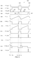
- FIG. 3 illustrates a timing diagram 300 of an embodiment of electrical waveforms of the bi-directional DC-DC converter 104 shown in FIG. 2 .
- the electrical waveform 306 represents a current of the power circuit 202 . It may be noted that the current shown in the electrical waveform 306 is shown crossing zero indicating the bi-directional DC-DC converter 104 with the soft switching topology 203 is operating in a discontinuous conduction mode.
- the electrical waveform 308 represents a voltage at the node 234 .
- the electrical waveform 310 represents a current through the lower semiconductor switch 206 .
- the electrical waveform 312 represents a voltage across the capacitor 232 and the electrical waveform 314 represents a current through the coupling circuit 224 .
- the electrical waveform 316 represents a voltage across the lower semiconductor switch 210 and the electrical waveform 318 represents a current through the lower semiconductor switch 210 . It may be noted that the electrical waveform 316 for the timing diagram 300 is illustrated having a zero voltage.
- the electrical waveforms 302 - 304 represent a voltage along the control bus received by the switching circuits 250 , 252 .
- the electrical waveform 302 represents a voltage of the gate terminal 221
- the electrical waveform 303 represents a voltage of the gate terminal 220
- the electrical waveform 303 represents a voltage of the gate terminal 222 .
- the electrical waveforms 302 - 304 include voltage peaks 320 - 325 representing activation of the corresponding semiconductor switches 206 , 208 , 210 .
- the voltage peaks 320 - 325 may represent voltage values over a threshold voltage of the semiconductor switches 206 , 208 , 210 activating the corresponding semiconductor switches 206 , 208 , 210 .
- a timing of the voltage peaks 320 - 325 is configured to boost the DC voltage received from the power supply 102 to the DC bus 116 , which is received by the power inverter circuit 106 .
- the timing diagram 300 is subdivided into set time periods and/or divisions (e.g., t 0 -t 7 ) based on the voltage peaks 320 - 325 representing a boost operation of the DC-DC converter 104 with the soft switching topology 203 .
- the controller circuit 108 deactivates the upper semiconductor switch 208 by adjusting the voltage along the control bus conductively coupled to the gate terminal 221 below the voltage threshold of the upper semiconductor switch 208 .
- voltage of the coupling circuit 224 is discharged. For example, a current traverses along the diode 229 through the coupling circuit 224 and the power circuit 202 (e.g., shown as a negative current by the electrical waveform 306 ).
- the voltage across the coupling circuit 224 is discharged (e.g., 0), and current traverses through the diode 227 and the power circuit 202 .
- a negative current through the power circuit 202 is constant, as shown in the electric waveform 306 , between t 1 and t 2 . It may be noted that the negative current may be utilized to charge the power source 102 .
- the controller circuit 108 activates the lower semiconductor switch 206 by adjusting the voltage along the control bus, shown as the voltage peak 321 , conductively coupled to the gate terminal 220 above the voltage threshold.
- the activation of the lower semiconductor switch 206 represents a zero voltage switching.
- the negative current through the power circuit 202 held the voltage across the lower semiconductor switch 206 at zero, shown by the electric waveform 308 at t 2 .
- the controller circuit 108 activates the lower semiconductor switch 210 by adjusting the voltage along the control bus, shown as the voltage peak 322 , conductively coupled to the gate terminal 222 above the voltage threshold.
- the activation of the lower semiconductor switch 210 represents a zero voltage switching.
- a voltage at the nodes 234 and 236 are zero when the lower semiconductor switch 210 is activated, as shown in the electric waveform 316 .
- a current through the lower semiconductor switch 210 is zero, as shown in the electric waveform 318 . It may be noted that the current through the power circuit 202 continues to increase linearly, as shown in the electric waveform 306 .
- the controller circuit 108 deactivates the lower semiconductor switch 206 by adjusting the voltage along the control bus conductively coupled to the gate terminal 220 below the voltage threshold of the lower semiconductor switch 206 . Based on the deactivation of the lower semiconductor switch 206 , current traverses along the power circuit 202 to the coupling circuit 224 and through the lower semiconductor switch 210 thereby charging the coupling circuit 224 as shown in the electric waveforms 312 and 314 and producing a voltage at the node 234 (shown at the electric waveform 308 ). The voltage at node 234 increases linearly, and is received at the DC bus 116 across the diode 228 at a controlled rate of rise defined by the coupling circuit 224 and a load current through the DC bus 116 . For example, the controller rate may be based on the electrical properties (e.g., capacitance) of the capacitor 232 of the coupling circuit 224 .
- the current through the power circuit 202 continues to flow through the diode 228 and to the DC bus 116 .
- the controller circuit 108 activates the upper semiconductor switch 208 by adjusting the voltage along the control bus, shown as the voltage peak 323 , conductively coupled to the gate terminal 221 above the voltage threshold. Additionally, the controller circuit 108 deactivates the lower semiconductor switch 210 by adjusting the voltage along the control bus conductively coupled to the gate terminal 222 below the voltage threshold of the lower semiconductor switch 210 . It may be noted the activation of the upper semiconductor switch 208 represents a zero voltage switching. For example, power circuit 202 continually discharges energy (e.g., current, voltage) to the DC bus 116 across the diode 228 (shown in t 5 ), which held the voltage across the upper semiconductor 208 to zero thereby enabling zero voltage switching. The power circuit 202 continually discharges as represented by the linear reduction in current shown in the electric waveform 306 .
- energy e.g., current, voltage
- the controller circuit 108 may continually and/or intermittently repeat the time periods t 0 -t 7 based on the operational mode of the electric motor 112 to boost a DC voltage and/or current.
- the soft switching topology 203 is configured to enable the DC-DC converter 104 to operate similar and/or the same operations (e.g., buck, boost) between the power source 102 and the power inverter circuit 106 .
- the controller circuit 108 may instruct the bi-directional DC-DC converter 104 with the soft switching topology 203 to buck (e.g., decrease the DC voltage) the DC voltage and/or current received from the power inverter circuit 106 into another DC voltage and/or current that is configured to recharging and/or charging the power source 102 .
- the controller circuit 108 is configured to reduce a voltage received by the power inverter circuit 106 based on activations and/or deactivations of at least one of the upper and/or lower semiconductor switches 206 , 208 , 210 , 212 at predetermined intervals.
- the controller circuit 108 may switch the activation and/or deactivation of the upper and/or lower semiconductor switches 206 , 208 , 210 , 212 relative to the timing diagram 300 to reduce the voltage and/or current along the DC bus 116 and delivered to the power source 102 .
- the controller circuit 108 may activate the lower switch 210 at t 2 until t 4 , the lower switch 206 at t 3 until t 6 , and the upper switch 212 at t 6 until t 7 .
- the DC-DC converter 104 with the soft switching topology 203 shown in FIG. 2 is shown operating in the discontinuous conduction mode.
- the DC-DC converter 104 with the soft switching topology 403 may be configured to operate in a discontinuous conduction mode and/or a continuous conduction mode.
- FIG. 4 illustrates a schematic illustration 400 of an embodiment of a soft switching topology 403 for a bi-directional DC-DC converter 104 configured to operate in continuous or discontinuous conduction modes.
- the schematic illustration 400 includes a second auxiliary switching circuit having an upper semiconductor switch 404 and a lower semiconductor switch 406 .
- the upper and lower semiconductor switches 404 and 406 may be similar to and/or the same as the upper and/or lower semiconductor switches 206 , 208 , 210 , 212 .
- the upper and lower semiconductor switches 404 and 406 each may include a diode 410 , 412 in anti-parallel with respect to the corresponding upper and lower semiconductor switches 404 and 406 . Additionally or alternatively, the diodes 410 , 412 may be integrated into the upper and lower semiconductor switches 404 and 406 .
- the schematic illustration 400 includes a resonant circuit 414 conductively coupled to the node 236 and a node 418 .
- the node 418 is interposed between the upper and lower semiconductor switches 404 and 406 .
- the resonant circuit 414 may include an inductor 416 and/or coil.
- the resonant circuit 414 is configured to receive and/or transfer energy stored in the coupling circuit 224 , which is subsequently supplied to the DC bus 116 and the power converter circuit 106 .
- the controller circuit 108 is conductively coupled to the switching circuits 250 , 252 , and 402 via the control bus.
- the controller circuit 108 is configured to adjust an electrical characteristic (e.g., voltage, current) along the controller bus to control the activation and/or deactivation of the switching circuits 250 , 252 and 402 .
- the control bus may include a plurality of conductive wires conductively coupling gate terminals 220 - 223 , 408 - 409 of the upper and lower semiconductor switches 206 , 208 , 210 , 212 , 404 , 406 to the controller circuit 108 .
- the controller circuit 108 may adjust voltages along the control bus to one or more of the gate terminal 220 - 223 , and 408 - 409 enabling the controller circuit 108 to activate (e.g., voltage at the gate above a threshold) at least one of the upper and/or lower semiconductor switches 206 , 208 , 210 , 212 , 404 and 406 .
- the controller circuit 108 may activate and/or deactivate at least one of the upper and/or lower semiconductor switches 206 , 208 , 210 , 212 , 404 , 406 at predetermined time periods based on an operational status of the electric motor 112 .
- the operational status of the electric motor 112 may represents the generating mode and/or the traction mode.
- the controller circuit 108 may activate and/or deactivate the at least one of the upper and/or lower semiconductor switches 206 , 208 , 210 , 212 , 404 , 406 at predetermined intervals.
- the timing diagram 500 shows the activation and/or deactivation of at least one of the upper and/or lower semiconductor switches 206 , 208 , 210 , 212 , 404 , 406 to boost a DC voltage and/or current received by the power circuit 202 from the power source 102 to the power inverter circuit 106 based on the traction mode of the electric motor 112 .
- FIG. 5 illustrates a timing diagram 500 of an embodiment of electrical waveforms of the bi-directional DC-DC converter 104 with the soft switching topology 403 shown in FIG. 4 .
- the electrical waveform 506 represents a current of the power circuit 202 . It may be noted that the current shown in the electrical waveform 506 is shown above zero indicating the bi-directional DC-DC converter 104 with the soft switching topology 403 is operating in the continuous conduction mode.
- the electrical waveform 508 represents a voltage at the node 234 .
- the electrical waveform 510 represents a current through the lower semiconductor switch 206 .
- the electrical waveform 512 represents a voltage across the capacitor 232 and the electrical waveform 514 represents a current through the coupling circuit 224 .
- the electrical waveform 516 represents a current through the resonant circuit 414 .
- the electrical waveform 518 represents a voltage across the lower semiconductor switch 210 and the electrical waveform 520 represents a current through the lower semiconductor switch 210 .
- the electrical waveforms 502 - 505 represent a voltage along the control bus received by the switching circuits 250 , 252 , 402 .
- the electrical waveform 502 represents a voltage of the gate terminal 221
- the electrical waveform 503 represents a voltage of the gate terminal 220
- the electrical waveform 504 represents a voltage of the gate terminal 408
- the electrical waveform 505 represents a voltage of the gate terminal 222 .
- the electrical waveforms 502 - 505 include voltage peaks 521 - 528 representing activation of the corresponding semiconductor switches 206 , 208 , 210 , and 408 .
- the voltage peaks 521 - 528 may be similar to and/or the same as the voltage peaks 320 - 325 shown in FIG. 3 .
- a timing of the voltage peaks 521 - 528 such as the activation of the semiconductor switches 206 , 208 , 210 , 408 is configured to boost the DC voltage received from the power supply 102 to the DC bus 116 , which is received by the power inverter circuit 106 .
- the timing diagram 500 is subdivided into set time periods and/or divisions (e.g., t 0 -t 8 ) based on the voltage peaks 521 - 528 representing a boost operation of the DC-DC converter 104 with the soft switching topology 403 .
- the upper semiconductor switch 208 is activated, for example, the control bus provides a voltage at the gate terminal 221 that is above the voltage threshold of the upper semiconductor switch 208 .
- the controller circuit 108 activates the upper semiconductor switch 404 by adjusting the voltage along the control bus, shown as the voltage peak 521 , conductively coupled to the gate terminal 408 above the voltage threshold.
- voltage of the coupling circuit 224 is discharged.
- a current traverses from the coupling circuit 224 discharging the voltage from the coupling circuit 224 to the resonant circuit 414 (e.g., shown as a current by the electrical waveform 516 ).
- the controller circuit 108 deactivates the upper semiconductor switches 208 and 404 by adjusting the voltage along the control bus conductively coupled to the gate terminals 221 and 408 below the voltage threshold of the upper semiconductor switches 208 and 404 .
- the coupling circuit 224 is discharged (e.g., as shown in the electrical waveform 512 ) through the diode 230 to the DC bus 116 (e.g., between t 1 and t 2 , the energy stored in the capacitor 232 is transferred to the inductor 416 to be later transferred to the power inverter circuit 106 between t 2 and t 3 ).
- the electrical energy stored in the resonant circuit 414 is discharged. Additionally, the power circuit 202 is continuously providing voltage and/or current via the diode 228 of the upper semiconductor switch 208 to the DC bus 116 .
- the controller circuit 108 activates the lower semiconductor switch 206 by adjusting the voltage along the control bus, shown as the voltage peak 522 , conductively coupled to the gate terminal 220 above the voltage threshold. It may be noted that the current through the power circuit 202 starts increasing linearly, as shown in the waveform 506 .
- the controller circuit 108 activates the lower semiconductor switch 210 by adjusting the voltage along the control bus conductively coupled to the gate terminal 222 above the voltage threshold represented as the voltage peak 524 . Based on the activation of the lower semiconductor switch 206 , current continually traverses from the power source 102 and the power circuit 202 through the lower semiconductor switch 206 , which continually increases the current linearly across the power circuit 202 (e.g., as shown in the electric waveform 510 ).
- the controller circuit 108 deactivates the lower semiconductor switch 206 by adjusting the voltage along the control bus conductively coupled to the gate terminal 220 below the voltage threshold of the lower semiconductor switch 206 .
- Current traverses from the power source 102 to the power circuit 202 and the coupling circuit 224 through the lower semiconductor switch 210 , thereby charging the coupling circuit 224 (e.g., as shown in the electric waveform 512 , 514 ).
- the voltage of the coupling circuit 224 is similar to and/or the same as the voltage across the node 234 .
- the voltage of coupling circuit 224 and the node 234 increases linearly a voltage and/or current of the DC bus 116 at a controller rate.
- the rate of rise of the voltage of the coupling circuit 224 and the node 234 is based on the coupling circuit 224 and the power inverter circuit 106 .
- the controlled rise is based on the electrical characteristics of the capacitor 232 of the coupling circuit 224 and/or the power inverter circuit 106 .
- the current through the power circuit 202 continues to flow through the diode 228 and to the DC bus 116 .
- the controller circuit 108 activates the upper semiconductor switch 208 by adjusting the voltage along the control bus, shown as the voltage peak 523 , conductively coupled to the gate terminal 221 above the voltage threshold.
- the controller circuit 108 deactivates the lower semiconductor switch 210 by adjusting the voltage along the control bus conductively coupled to the gate terminal 222 below the voltage threshold of the lower semiconductor switch 210 .
- the activation of the upper semiconductor switch 208 represents a zero voltage switching.
- power circuit 202 continually discharges energy (e.g., current, voltage) to the DC bus 116 across the diode 228 (shown in t 6 ), which holds the voltage across the upper semiconductor 208 to zero thereby enabling zero voltage switching.
- the power circuit 202 continues to discharge as represented by the linear reduction in current shown in the electric waveform 306 .
- the controller circuit 108 may continually and/or intermittently repeat the time periods t 0 -t 8 based on the operational mode of the electric motor 112 to boost a DC voltage and/or current. It may be noted that when the controller circuit 108 determines an operational mode of the electric motor 112 to be the generating mode, the controller circuit 108 may instruct the bi-directional DC-DC converter to buck (e.g., decrease the DC voltage) the DC voltage and/or current received from the power inverter circuit 106 into another DC voltage and/or current that is configured to recharging and/or charge the power source 102 .
- buck e.g., decrease the DC voltage
- the controller circuit 108 is configured to reduce a voltage received by the power inverter circuit 106 based on activations and/or deactivations of at least one of the upper and/or lower semiconductor switches 206 , 208 , 210 , 212 , 404 , 406 at predetermined intervals.
- the controller circuit 108 may switch the activation and/or deactivation of the upper and/or lower semiconductor switches 206 , 208 , 210 , 212 , 404 , 406 relative to the timing diagram 500 to reduce the voltage and/or current along the DC bus 116 and delivered to the power source 102 .
- the soft switching topology 660 may be configured to form an interleaved boost DC-DC converter 662 .
- the interleaved boost DC-DC converter 662 is configured to boost a voltage and/or current of the power source 102 to a higher DC voltage and/or current along the DC bus 116 utilizing a plurality of phases.
- FIG. 6 illustrates a schematic illustration 650 of an embodiment of the soft switching topology 660 for the interleaved boost DC-DC converter 662 .
- the power circuit 202 includes two inductors 651 and 652 configured in parallel with each other.
- the soft switching topology 660 may be configured to interleave the switching circuits 250 and 252 based on a coupling circuit 224 .
- the coupling circuit 224 may include an inductor 656 in series with a capacitor 658 .
- the coupling circuit 224 is configured such that the switching circuits 250 and 252 are utilized to boost power to the DC bus 116 by having the switching circuits 250 and 252 operating at different phases with respect to each other.
- the coupling circuit 224 is configured to adjust a phase of the switching circuit 252 by 180° with respect to the switching circuit 250 as shown by the electrical waveforms 702 - 713 to define the interleaved boost DC-DC converter 662 .
- FIGS. 7 A-B illustrate timing diagrams 700 , 720 of the electrical waveforms 702 - 713 of the interleaved DC-DC converter 662 shown in FIG. 6 .
- the electrical waveform 702 represents a voltage across and the electrical waveform 703 represents a current through the lower semiconductor switch 206 .
- the electrical waveform 704 represents a voltage at the gate terminal 220 .
- the electrical waveform 705 represents a voltage across and the electrical waveform 706 represents a current through the lower semiconductor switch 210 .
- the electrical waveform 707 represents a voltage at the gate terminal 222 .
- the electrical waveform 708 represents a voltage across and the electrical waveform 709 represents a current through the upper semiconductor switch 208 .
- the electrical waveform 710 represents a voltage at the gate terminal 221 .
- the electrical waveform 711 represents a voltage across and the electrical waveform 712 represents a current through the upper semiconductor switch 223 .
- the electrical waveform 713 represents a voltage at the gate terminal 223 .
- the timing diagrams 700 , 720 are subdivided into set time periods and/or divisions (e.g., t 0 -t 1 ) corresponding to activation of the upper and/or lower semiconductor switches 206 , 208 , 210 , 212 of the interleaved DC-DC converter 662 with the soft switching topology 660 .
- the energy accumulated in the power circuit 202 (e.g., the inductors 651 , 652 ) during the time periods of the timing diagrams 700 , 720 of one of the switching circuits 250 , 252 is utilized to discharge the energy of the coupling circuit 224 in the other switching circuits 252 , 250 prior to activation of the associated upper and/or lower semiconductor switch 206 , 208 , 210 , 212 .
- the coupling circuit 224 operates as a resonant circuit based on the inductor 656 and capacitor 658 , which is utilized to generate a negative current.
- the negative current is used to discharge the capacitance of the alternative semiconductor switch 206 , 208 , 210 , 212 prior to the controller circuit 202 activating the upper and/or lower switch 206 , 208 , 210 , 212 along the control bus. Based on the discharge, the lower semiconductor switches 206 and 210 are activated at zero voltage switching operation, and the upper semiconductor switches 208 and 212 are activated at zero current operation.
- the lower semiconductor switch 206 and upper semiconductor switch 212 are activated. It may be noted at t 0 the electrical waveform 702 indicate no voltage across the lower semiconductor switch 206 , and the electrical waveform 712 indicate no current through the upper semiconductor switch 212 when activated. For example, the lower semiconductor switch 206 is activated at a zero voltage switching operation, and the upper semiconductor switch 212 is activated at a zero current switching operation.
- the control bus provides a voltage at the gate terminals 220 and 223 above the voltage thresholds of the lower and upper semiconductor switches 206 and 208 . As shown between t 0 and t 1 of the electrical waveforms 703 and 712 , current traverses through the lower and upper semiconductor switches 206 , 212 .
- electrical energy is discharged in the power circuit 202 (e.g., by the inductors 651 and 652 ) by the switching circuit 250 shown as a positive current in the electrical waveform 703 .
- electrical energy accumulated in the coupling circuit 224 is discharged by the switching circuit 252 shown as a decrease in current through the upper semiconductor switch 212 shown as the electrical waveform 712 .
- the controller circuit 108 deactivates the lower and upper semiconductor switches 206 and 212 by adjusting the voltage along the control bus conductively coupled to the gate terminals 220 and 223 below the voltage threshold.
- the controller circuit 108 activates the lower and upper semiconductor switches 210 and 208 .
- Electrical energy is accumulated in the power circuit 202 (e.g., by the inductors 651 and 652 ) by the switching circuit 250 shown as a negative current in the electrical waveform 706 .
- electrical energy is accumulated in the coupling circuit 224 , such as at the capacitor 658 , by the switching circuit 252 shown as an increase in current through the lower semiconductor switch 210 shown as the electrical waveform 712 .
- FIG. 8 is a flow chart of an embodiment of a method for soft switching a DC-DC converter.
- the method 600 may employ or be performed by structures or aspects of various embodiments discussed herein.
- certain operations may be omitted or added, certain operations may be combined, certain operations may be performed simultaneously, certain operations may be performed concurrently, certain operations may be split into multiple operations, certain operations may be performed in a different order, or certain operations or series of operations may be re-performed in an iterative fashion.
- portions, aspects, and/or variations of the method 600 may be able to be used as one or more algorithms to direct hardware to perform one or more operations described herein.
- the operational status of the electric motor 112 may represent the generating mode and/or the traction mode.
- the controller circuit 108 may determine the operational status of the electric motor 112 based on a sensor (not shown) measuring a voltage and/or current of the DC bus 116 . Additionally or alternatively, the controller circuit 108 may determine the operational status of the electric motor 112 based on operation of the vehicle, such as by activation of pedals of the vehicle. For example, activation of the gas and/or accelerator pedal may indicate to the controller circuit 108 that the electric motor 112 is operating in the traction mode. Alternatively, activation of the brake pedal may indicate to the controller circuit 108 that the electric motor 112 is operating in the generating mode.
- the controller circuit 108 determines whether the electric motor 112 is in a traction mode. For example, based on the activation of the gas and/or accelerator pedal the controller circuit 108 may determine that the electric motor 112 is in a traction mode.
- the controller circuit 108 is configured to activate at least one of an upper or lower semiconductor switches 206 , 208 , 210 , 212 corresponding to a boost mode of the DC-DC converter 104 with the soft switching topology 203 .
- the controller circuit 108 may activate at least one of an upper or lower semiconductor switches 206 , 208 , 210 , 212 by adjusting a voltage along the control bus corresponding to the electric waveforms 302 - 304 .
- the controller circuit 108 may activate at least one of an upper or lower semiconductor switches 206 , 208 , 210 , 212 , 404 , 406 by adjusting a voltage along the control bus corresponding to the electric waveforms 502 - 505 .
- the controller circuit 108 is configured to deliver the adjusted voltage to the power converter circuit 106 .
- the controller circuit 108 based on the activation of at least one of an upper or lower semiconductor switches 206 , 208 , 210 , 212 may deliver the boosted voltage of the power source 102 along the DC bus 116 conductively coupled to the power converter circuit 106 .
- the controller circuit 108 is configured to activate at least one of an upper or lower semiconductor switches 206 , 208 , 210 , 212 corresponding to a buck mode of the DC-DC converter 104 with the soft switching topology 203 .
- the controller circuit 108 may switch the activation and/or deactivation of the upper and/or lower semiconductor switches 206 , 208 , 210 , 212 relative to the timing diagram 300 to reduce the voltage and/or current along the DC bus 116 and delivered to the power source 102 .
- the controller circuit 108 is configured to deliver the adjusted voltage to the power source 102 .
- the controller circuit 108 based on the activation of at least one of an upper or lower semiconductor switches 206 , 208 , 210 , 212 may deliver the reduced or bucked voltage of the DC bus 116 received from the power converter circuit 106 to the power circuit 202 , which is conductively coupled to the power source 102 .
- the particular arrangement of components (e.g., the number, types, placement, and/or the like) of the illustrated embodiments may be modified in various alternate embodiments.
- different numbers of a given module or unit may be employed, a different type or types of a given module or unit may be employed, a number of modules or units (or aspects thereof) may be combined, a given module or unit may be divided into plural modules (or sub-modules) or units (or sub-units), one or more aspects of one or more modules may be shared between modules, a given module or unit may be added, or a given module or unit may be omitted.
- a structure, limitation, or element that is “configured to” perform a task or operation is particularly structurally formed, constructed, or adapted in a manner corresponding to the task or operation.
- an object that is merely capable of being modified to perform the task or operation is not “configured to” perform the task or operation as used herein.
- the use of “configured to” as used herein denotes structural adaptations or characteristics, and denotes structural requirements of any structure, limitation, or element that is described as being “configured to” perform the task or operation.
- a processing unit, processor, or computer that is “configured to” perform a task or operation may be understood as being particularly structured to perform the task or operation (e.g., having one or more programs or instructions stored thereon or used in conjunction therewith tailored or intended to perform the task or operation, and/or having an arrangement of processing circuitry tailored or intended to perform the task or operation).
- a general purpose computer which may become “configured to” perform the task or operation if appropriately programmed) is not “configured to” perform a task or operation unless or until specifically programmed or structurally modified to perform the task or operation.
- the various embodiments may be implemented in hardware, software or a combination thereof.
- the various embodiments and/or components also may be implemented as part of one or more computers or processors.
- the computer or processor may include a computing device, an input device, a display unit and an interface, for example, for accessing the Internet.
- the computer or processor may include a microprocessor.
- the microprocessor may be connected to a communication bus.
- the computer or processor may also include a memory.
- the memory may include Random Access Memory (RAM) and Read Only Memory (ROM).
- the computer or processor further may include a storage device, which may be a hard disk drive or a removable storage drive such as a solid state drive, optic drive, and the like.
- the storage device may also be other similar means for loading computer programs or other instructions into the computer or processor.
- the term “computer,” “controller,” and “module” may each include any processor-based or microprocessor-based system including systems using microcontrollers, reduced instruction set computers (RISC), application specific integrated circuits (ASICs), logic circuits, GPUs, FPGAs, and any other circuit or processor capable of executing the functions described herein.
- RISC reduced instruction set computers
- ASICs application specific integrated circuits
- GPUs GPUs
- FPGAs field-programmable gate arrays
- the computer, module, or processor executes a set of instructions that are stored in one or more storage elements, in order to process input data.
- the storage elements may also store data or other information as desired or needed.
- the storage element may be in the form of an information source or a physical memory element within a processing machine.
- the set of instructions may include various commands that instruct the computer, module, or processor as a processing machine to perform specific operations such as the methods and processes of the various embodiments described and/or illustrated herein.
- the set of instructions may be in the form of a software program.
- the software may be in various forms such as system software or application software and which may be embodied as a tangible and non-transitory computer readable medium. Further, the software may be in the form of a collection of separate programs or modules, a program module within a larger program or a portion of a program module.
- the software also may include modular programming in the form of object-oriented programming.
- the processing of input data by the processing machine may be in response to operator commands, or in response to results of previous processing, or in response to a request made by another processing machine.
- the terms “software” and “firmware” are interchangeable, and include any computer program stored in memory for execution by a computer, including RAM memory, ROM memory, EPROM memory, EEPROM memory, and non-volatile RAM (NVRAM) memory.
- RAM memory random access memory
- ROM memory read-only memory
- EPROM memory erasable programmable read-only memory
- EEPROM memory electrically erasable programmable read-only memory
- NVRAM non-volatile RAM
- the individual components of the various embodiments may be virtualized and hosted by a cloud type computational environment, for example to allow for dynamic allocation of computational power, without requiring the user concerning the location, configuration, and/or specific hardware of the computer system.
Landscapes
- Engineering & Computer Science (AREA)
- Power Engineering (AREA)
- Dc-Dc Converters (AREA)
- Inverter Devices (AREA)
Abstract
Description
Claims (20)
Applications Claiming Priority (2)
| Application Number | Priority Date | Filing Date | Title |
|---|---|---|---|
| CN201710061052.3 | 2017-01-25 | ||
| CN201710061052.3A CN108347167B (en) | 2017-01-25 | 2017-01-25 | System and method for soft switching DC-DC converter |
Publications (2)
| Publication Number | Publication Date |
|---|---|
| US20180212545A1 US20180212545A1 (en) | 2018-07-26 |
| US11784600B2 true US11784600B2 (en) | 2023-10-10 |
Family
ID=62906695
Family Applications (1)
| Application Number | Title | Priority Date | Filing Date |
|---|---|---|---|
| US15/834,304 Active US11784600B2 (en) | 2017-01-25 | 2017-12-07 | Systems and methods for a soft switching DC-DC converter |
Country Status (4)
| Country | Link |
|---|---|
| US (1) | US11784600B2 (en) |
| JP (1) | JP7045859B2 (en) |
| KR (1) | KR102400368B1 (en) |
| CN (1) | CN108347167B (en) |
Cited By (4)
| Publication number | Priority date | Publication date | Assignee | Title |
|---|---|---|---|---|
| US20230084872A1 (en) * | 2020-03-10 | 2023-03-16 | Khalifa University of Science and Technology | Ultra high gain bidirectional dc to dc converter |
| US20240198809A1 (en) * | 2022-12-14 | 2024-06-20 | Zf Friedrichshafen Ag | Electric drive system, control method and related equipment |
| US20240266959A1 (en) * | 2022-07-21 | 2024-08-08 | Southeast University | Control method for four-switch buck-boost converter |
| US12267014B2 (en) * | 2020-04-29 | 2025-04-01 | Huawei Technologies Co., Ltd. | Non-isolated DCDC resonant conversion control circuit and control method |
Families Citing this family (12)
| Publication number | Priority date | Publication date | Assignee | Title |
|---|---|---|---|---|
| FR3064849B1 (en) * | 2017-03-31 | 2019-06-07 | Centum Adetel Transportation | HYBRID POWER CELL |
| DE102018204865A1 (en) * | 2018-03-29 | 2019-10-02 | Siemens Aktiengesellschaft | Circuit arrangement with a spacer element, converter and aircraft with such a circuit arrangement and method for current measurement |
| CN108512431B (en) * | 2018-04-24 | 2019-08-27 | 上海推拓科技有限公司 | Dual rectifier interleaved full-bridge single-stage power factor correction power supply circuit and control method |
| CN108471232B (en) * | 2018-04-24 | 2019-10-08 | 上海推拓科技有限公司 | Double rectifier bridge formula single stage power factor correction power circuit |
| JP7142527B2 (en) * | 2018-09-13 | 2022-09-27 | Ntn株式会社 | Coupled inductors and switching circuits |
| CN110829838B (en) * | 2019-10-28 | 2021-07-02 | 南通大学 | A Zero-Voltage Soft-Switching Bidirectional Buck/Boost Converter |
| KR102803716B1 (en) * | 2020-04-02 | 2025-05-09 | 엘지전자 주식회사 | Method for discharging capacitor of resonant power conversion apparatus at initiating of operation and resonant power conversion apparatus thereof |
| DE102020006324A1 (en) | 2020-10-15 | 2022-04-21 | Kostal Automobil Elektrik Gmbh & Co. Kg | Electrical voltage converter with an active snubber |
| TWI832074B (en) * | 2021-08-02 | 2024-02-11 | 崑山科技大學 | Interleaved high step-up dc converter |
| US12328080B2 (en) | 2021-10-28 | 2025-06-10 | Carrier Corporation | Boost converter state control |
| KR20230119440A (en) | 2022-02-07 | 2023-08-16 | 현대자동차주식회사 | Motor driving apparatus and method |
| US20230312084A1 (en) * | 2022-04-04 | 2023-10-05 | Honeywell International Inc. | Aircraft high-voltage actuator controller with embedded bidirectional dc/dc converter |
Citations (52)
| Publication number | Priority date | Publication date | Assignee | Title |
|---|---|---|---|---|
| US5412557A (en) | 1992-10-14 | 1995-05-02 | Electronic Power Conditioning, Inc. | Unipolar series resonant converter |
| US5412577A (en) | 1992-10-28 | 1995-05-02 | Quad/Tech International | Color registration system for a printing press |
| CN1104002A (en) | 1993-12-15 | 1995-06-21 | 许天昀 | Method for controlling resonance power conversion |
| US5594635A (en) | 1993-03-30 | 1997-01-14 | Motorola, Inc. | Constant frequency, zero-voltage-switching converters with resonant switching bridge |
| US6370050B1 (en) | 1999-09-20 | 2002-04-09 | Ut-Batelle, Llc | Isolated and soft-switched power converter |
| JP2005261059A (en) | 2004-03-11 | 2005-09-22 | Toyota Industries Corp | Current bidirectional converter |
| TWI262646B (en) | 2005-07-13 | 2006-09-21 | Wai Zheng Zhong | High-efficiency bidirectional converter for power sources with great voltage diversity |
| US7382113B2 (en) | 2006-03-17 | 2008-06-03 | Yuan Ze University | High-efficiency high-voltage difference ratio bi-directional converter |
| US20090046482A1 (en) * | 2007-08-13 | 2009-02-19 | Stephen William Smith | Phase shifted H-Bridge resonant converter with symmetrical currents |
| US20090051346A1 (en) * | 2005-03-31 | 2009-02-26 | Kota Manabe | Voltage Conversion Device and Vehicle |
| CN101447743A (en) | 2007-11-30 | 2009-06-03 | 日立空调·家用电器株式会社 | Electric power converter and control method for the same |
| US20090196072A1 (en) * | 2007-12-03 | 2009-08-06 | Zhong Ye | Phase-shifted dual-bridge DC/DC converter with wide-range ZVS and zero circulating current |
| CN101577489A (en) | 2009-05-14 | 2009-11-11 | 湖南银河电气有限公司 | Soft switching converter suitable for sensitive bidirectional current loads |
| US7812575B2 (en) | 2006-04-14 | 2010-10-12 | Hitachi Computer Peripherals Co., Ltd. | Bidirectional DC-DC converter and power supply apparatus with the same |
| JP4562961B2 (en) | 2001-07-19 | 2010-10-13 | 本田技研工業株式会社 | Resonant bidirectional DC-DC converter and control method thereof |
| KR20100114751A (en) | 2009-04-16 | 2010-10-26 | 서울과학기술대학교 산학협력단 | Bi-directional non-isolated dc-dc converter and control method thereof |
| US20110095742A1 (en) * | 2008-04-16 | 2011-04-28 | Douglas Dean Lopata | Power Converter with Controller Operable in Selected Modes of Operation |
| JP2011097740A (en) | 2009-10-29 | 2011-05-12 | Toyota Motor Corp | Power converter |
| US20120049773A1 (en) * | 2010-08-27 | 2012-03-01 | Denso Corporation | Motor control apparatus which discharges stored charge of dc voltage smoothing capacitor when operation becomes halted |
| US8174849B2 (en) | 2008-02-28 | 2012-05-08 | Fuji Electric Co., Ltd. | Electric power converter with soft switching for two way power conversion |
| US20120112702A1 (en) * | 2010-11-05 | 2012-05-10 | Robert Louis Steigerwald | Apparatus for transferring energy using onboard power electronics with high-frequency transformer isolation and method of manufacturing same |
| US20120140524A1 (en) * | 2010-12-01 | 2012-06-07 | Daihen Corporation | Power supply and arc processing power supply |
| TW201308840A (en) | 2011-08-12 | 2013-02-16 | Nat Univ Chung Cheng | Active damping circuit capable of performing soft-switching |
| US8593845B2 (en) | 2009-06-11 | 2013-11-26 | Toyota Jidosha Kabushiki Kaisha | Converter controller |
| US20130322126A1 (en) * | 2012-05-30 | 2013-12-05 | National Tsing Hua University | Soft-Switching Inverter |
| US8644035B2 (en) | 2012-02-24 | 2014-02-04 | Majid Pahlevaninezhad | Load adaptive variable frequency phase-shift full-bridge DC/DC converter |
| CN103715923A (en) | 2012-10-01 | 2014-04-09 | 财团法人工业技术研究院 | Direct current-alternating current conversion circuit |
| KR101395569B1 (en) | 2013-06-26 | 2014-05-21 | 전남대학교산학협력단 | Resonant dc/dc converter using the source |
| US20140217974A1 (en) * | 2013-02-06 | 2014-08-07 | Lg Electronics Inc. | Charging apparatus and electric vehicle including the same |
| TWI465024B (en) | 2012-09-19 | 2014-12-11 | Nat Univ Chin Yi Technology | Bidirectional buck-boost converter with soft-switching |
| US20150048810A1 (en) | 2012-03-16 | 2015-02-19 | Sanken Electric Co., Ltd. | Bidirectional dc-dc converter |
| CN104578773A (en) | 2014-12-30 | 2015-04-29 | 西安理工大学 | Soft switching circuit for bidirectional DC/DC (direct current/direct current) converter and control method |
| CN103036430B (en) | 2012-12-28 | 2015-04-29 | 深圳市航天新源科技有限公司 | Low-ripple bidirectional soft-switching direct current-direct current (DC-DC) circuit |
| CN104604089A (en) | 2012-09-05 | 2015-05-06 | 富士机械制造株式会社 | Non-contact power supply device |
| CN104737432A (en) | 2012-08-27 | 2015-06-24 | 庞巴迪运输有限公司 | Adaptive soft switching control for power converter |
| US20150194909A1 (en) | 2014-01-08 | 2015-07-09 | Majid Pahlevaninezhad | Zvs voltage source inverter |
| US9093912B2 (en) | 2013-03-15 | 2015-07-28 | Illinois Tool Works Inc. | Method and apparatus for soft switching welding type power |
| CN102832809B (en) | 2012-08-07 | 2015-08-05 | 燕山大学 | Adjustment of inductance switched capacitor passive clamping soft switch high gain boost code converter |
| US20150229252A1 (en) * | 2012-11-28 | 2015-08-13 | Fuji Electric Co., Ltd. | Power conversion system and control method thereof |
| CN105207486A (en) | 2015-09-06 | 2015-12-30 | 南京航空航天大学 | Bidirectional resonance DC converter and control method thereof |
| JP2016025831A (en) | 2014-07-24 | 2016-02-08 | 国立大学法人神戸大学 | Auxiliary circuit of dc-dc converter, and bidirectional step-up/down dc-dc converter arranged by use thereof |
| US20160043631A1 (en) | 2014-08-11 | 2016-02-11 | Asian Power Devices Inc. | Passive coupled-inductor soft-switching circuit of power factor correctors |
| US20160094133A1 (en) | 2013-05-30 | 2016-03-31 | Nissan Motor Co., Ltd. | Dc-dc converter and control method thereof |
| US9307587B1 (en) | 2013-07-19 | 2016-04-05 | Universal Lighting Technologies, Inc. | Constant current source based on self-oscillating soft-switching LLC converter topology |
| US20160099647A1 (en) | 2014-10-02 | 2016-04-07 | Navitas Semiconductor Inc. | Zero Voltage Soft Switching Scheme for Power Converters |
| US20160111964A1 (en) | 2014-10-17 | 2016-04-21 | Rohm Co., Ltd. | Switch driving circuit and switching power device using the same |
| US20160141960A1 (en) | 2014-11-19 | 2016-05-19 | Futurewei Technologies, Inc. | Zero Voltage Switching Detection Apparatus and Method |
| JP2016092854A (en) | 2014-10-29 | 2016-05-23 | 株式会社デンソー | Power converter |
| US20160152129A1 (en) | 2013-08-06 | 2016-06-02 | Volvo Truck Corporation | Hybrid vehicle |
| US9362827B2 (en) | 2014-06-25 | 2016-06-07 | Delta Electronics, Inc. | Soft-switching bi-directional power converter and method of operating the same |
| US9419522B1 (en) | 2013-02-13 | 2016-08-16 | University Of Maryland | ZVS DC/DC converter for converting voltage between a battery and a DC link in a hybrid energy storage system and method thereof |
| US20180154787A1 (en) * | 2016-12-01 | 2018-06-07 | Ford Global Technologies, Llc | Adaptive Boost Voltage For Hybrid Vehicle Operation |
Family Cites Families (1)
| Publication number | Priority date | Publication date | Assignee | Title |
|---|---|---|---|---|
| WO2012168847A1 (en) * | 2011-06-10 | 2012-12-13 | Koninklijke Philips Electronics N.V. | Dc- dc driver device having input and output filters, for driving a load, in particular an led unit |
-
2017
- 2017-01-25 CN CN201710061052.3A patent/CN108347167B/en active Active
- 2017-12-07 US US15/834,304 patent/US11784600B2/en active Active
-
2018
- 2018-01-12 JP JP2018003029A patent/JP7045859B2/en active Active
- 2018-01-23 KR KR1020180008307A patent/KR102400368B1/en active Active
Patent Citations (53)
| Publication number | Priority date | Publication date | Assignee | Title |
|---|---|---|---|---|
| US5412557A (en) | 1992-10-14 | 1995-05-02 | Electronic Power Conditioning, Inc. | Unipolar series resonant converter |
| US5412577A (en) | 1992-10-28 | 1995-05-02 | Quad/Tech International | Color registration system for a printing press |
| US5594635A (en) | 1993-03-30 | 1997-01-14 | Motorola, Inc. | Constant frequency, zero-voltage-switching converters with resonant switching bridge |
| CN1104002A (en) | 1993-12-15 | 1995-06-21 | 许天昀 | Method for controlling resonance power conversion |
| US6370050B1 (en) | 1999-09-20 | 2002-04-09 | Ut-Batelle, Llc | Isolated and soft-switched power converter |
| JP4562961B2 (en) | 2001-07-19 | 2010-10-13 | 本田技研工業株式会社 | Resonant bidirectional DC-DC converter and control method thereof |
| JP2005261059A (en) | 2004-03-11 | 2005-09-22 | Toyota Industries Corp | Current bidirectional converter |
| US20090051346A1 (en) * | 2005-03-31 | 2009-02-26 | Kota Manabe | Voltage Conversion Device and Vehicle |
| TWI262646B (en) | 2005-07-13 | 2006-09-21 | Wai Zheng Zhong | High-efficiency bidirectional converter for power sources with great voltage diversity |
| US7382113B2 (en) | 2006-03-17 | 2008-06-03 | Yuan Ze University | High-efficiency high-voltage difference ratio bi-directional converter |
| US7812575B2 (en) | 2006-04-14 | 2010-10-12 | Hitachi Computer Peripherals Co., Ltd. | Bidirectional DC-DC converter and power supply apparatus with the same |
| US20090046482A1 (en) * | 2007-08-13 | 2009-02-19 | Stephen William Smith | Phase shifted H-Bridge resonant converter with symmetrical currents |
| CN101447743A (en) | 2007-11-30 | 2009-06-03 | 日立空调·家用电器株式会社 | Electric power converter and control method for the same |
| US20090196072A1 (en) * | 2007-12-03 | 2009-08-06 | Zhong Ye | Phase-shifted dual-bridge DC/DC converter with wide-range ZVS and zero circulating current |
| US8174849B2 (en) | 2008-02-28 | 2012-05-08 | Fuji Electric Co., Ltd. | Electric power converter with soft switching for two way power conversion |
| US20110095742A1 (en) * | 2008-04-16 | 2011-04-28 | Douglas Dean Lopata | Power Converter with Controller Operable in Selected Modes of Operation |
| KR20100114751A (en) | 2009-04-16 | 2010-10-26 | 서울과학기술대학교 산학협력단 | Bi-directional non-isolated dc-dc converter and control method thereof |
| CN101577489A (en) | 2009-05-14 | 2009-11-11 | 湖南银河电气有限公司 | Soft switching converter suitable for sensitive bidirectional current loads |
| US8593845B2 (en) | 2009-06-11 | 2013-11-26 | Toyota Jidosha Kabushiki Kaisha | Converter controller |
| JP2011097740A (en) | 2009-10-29 | 2011-05-12 | Toyota Motor Corp | Power converter |
| US20120049773A1 (en) * | 2010-08-27 | 2012-03-01 | Denso Corporation | Motor control apparatus which discharges stored charge of dc voltage smoothing capacitor when operation becomes halted |
| US20120112702A1 (en) * | 2010-11-05 | 2012-05-10 | Robert Louis Steigerwald | Apparatus for transferring energy using onboard power electronics with high-frequency transformer isolation and method of manufacturing same |
| US20120140524A1 (en) * | 2010-12-01 | 2012-06-07 | Daihen Corporation | Power supply and arc processing power supply |
| TW201308840A (en) | 2011-08-12 | 2013-02-16 | Nat Univ Chung Cheng | Active damping circuit capable of performing soft-switching |
| US8644035B2 (en) | 2012-02-24 | 2014-02-04 | Majid Pahlevaninezhad | Load adaptive variable frequency phase-shift full-bridge DC/DC converter |
| US20150048810A1 (en) | 2012-03-16 | 2015-02-19 | Sanken Electric Co., Ltd. | Bidirectional dc-dc converter |
| US20130322126A1 (en) * | 2012-05-30 | 2013-12-05 | National Tsing Hua University | Soft-Switching Inverter |
| CN102832809B (en) | 2012-08-07 | 2015-08-05 | 燕山大学 | Adjustment of inductance switched capacitor passive clamping soft switch high gain boost code converter |
| US20150318784A1 (en) * | 2012-08-27 | 2015-11-05 | Bombardier Transportation Gmbh | Adaptive Soft Switching Control For Power Converter |
| CN104737432A (en) | 2012-08-27 | 2015-06-24 | 庞巴迪运输有限公司 | Adaptive soft switching control for power converter |
| CN104604089A (en) | 2012-09-05 | 2015-05-06 | 富士机械制造株式会社 | Non-contact power supply device |
| TWI465024B (en) | 2012-09-19 | 2014-12-11 | Nat Univ Chin Yi Technology | Bidirectional buck-boost converter with soft-switching |
| CN103715923A (en) | 2012-10-01 | 2014-04-09 | 财团法人工业技术研究院 | Direct current-alternating current conversion circuit |
| US20150229252A1 (en) * | 2012-11-28 | 2015-08-13 | Fuji Electric Co., Ltd. | Power conversion system and control method thereof |
| CN103036430B (en) | 2012-12-28 | 2015-04-29 | 深圳市航天新源科技有限公司 | Low-ripple bidirectional soft-switching direct current-direct current (DC-DC) circuit |
| US20140217974A1 (en) * | 2013-02-06 | 2014-08-07 | Lg Electronics Inc. | Charging apparatus and electric vehicle including the same |
| US9419522B1 (en) | 2013-02-13 | 2016-08-16 | University Of Maryland | ZVS DC/DC converter for converting voltage between a battery and a DC link in a hybrid energy storage system and method thereof |
| US9093912B2 (en) | 2013-03-15 | 2015-07-28 | Illinois Tool Works Inc. | Method and apparatus for soft switching welding type power |
| US20160094133A1 (en) | 2013-05-30 | 2016-03-31 | Nissan Motor Co., Ltd. | Dc-dc converter and control method thereof |
| KR101395569B1 (en) | 2013-06-26 | 2014-05-21 | 전남대학교산학협력단 | Resonant dc/dc converter using the source |
| US9307587B1 (en) | 2013-07-19 | 2016-04-05 | Universal Lighting Technologies, Inc. | Constant current source based on self-oscillating soft-switching LLC converter topology |
| US20160152129A1 (en) | 2013-08-06 | 2016-06-02 | Volvo Truck Corporation | Hybrid vehicle |
| US20150194909A1 (en) | 2014-01-08 | 2015-07-09 | Majid Pahlevaninezhad | Zvs voltage source inverter |
| US9362827B2 (en) | 2014-06-25 | 2016-06-07 | Delta Electronics, Inc. | Soft-switching bi-directional power converter and method of operating the same |
| JP2016025831A (en) | 2014-07-24 | 2016-02-08 | 国立大学法人神戸大学 | Auxiliary circuit of dc-dc converter, and bidirectional step-up/down dc-dc converter arranged by use thereof |
| US20160043631A1 (en) | 2014-08-11 | 2016-02-11 | Asian Power Devices Inc. | Passive coupled-inductor soft-switching circuit of power factor correctors |
| US20160099647A1 (en) | 2014-10-02 | 2016-04-07 | Navitas Semiconductor Inc. | Zero Voltage Soft Switching Scheme for Power Converters |
| US20160111964A1 (en) | 2014-10-17 | 2016-04-21 | Rohm Co., Ltd. | Switch driving circuit and switching power device using the same |
| JP2016092854A (en) | 2014-10-29 | 2016-05-23 | 株式会社デンソー | Power converter |
| US20160141960A1 (en) | 2014-11-19 | 2016-05-19 | Futurewei Technologies, Inc. | Zero Voltage Switching Detection Apparatus and Method |
| CN104578773A (en) | 2014-12-30 | 2015-04-29 | 西安理工大学 | Soft switching circuit for bidirectional DC/DC (direct current/direct current) converter and control method |
| CN105207486A (en) | 2015-09-06 | 2015-12-30 | 南京航空航天大学 | Bidirectional resonance DC converter and control method thereof |
| US20180154787A1 (en) * | 2016-12-01 | 2018-06-07 | Ford Global Technologies, Llc | Adaptive Boost Voltage For Hybrid Vehicle Operation |
Non-Patent Citations (18)
| Title |
|---|
| Chao et al., "Bidirectional DC-DC soft-switching converter for stand-alone photovoltaic power generation systems", in IET Power Electronics, vol. 7, issue: 6, pp. 1557-1565, Jun. 2014. |
| Elmes et al., "Modular bidirectional DC-DC converter for hybrid/electric vehicles with variable-frequency interleaved soft-switching", Vehicle Power and Propulsion Conference, 2009. VPPC '09. IEEE, pp. 448-454,2009, Dearborn, MI. |
| English Translation and First Chinese Office Action and Search Report for corresponding CN 201710061052.3, dated Aug. 23, 2019. |
| English Translation of Japanese Office Action for corresponding JP Application No. 2018-003029, dated Nov. 15, 2021. |
| English translation of Korean Office Action for corresponding KR Application No. 1020180008307, dated Sep. 29, 2021. |
| Gang et al., "A Novel Soft Switching Bidirectional DC/DC Converter and Design Consideration", Power Electronics and Motion Control Conference, 2006. IPEMC 2006. CES/IEEE 5th International, pp. 1-4, 2006, Shanghai. |
| H L Do, "Nonisolated Bidirectional Zero-Voltage-Switching DC-DC Converter", IEEE Transactions on Power Electronics,vol. 26, Issue: 9, pp. 2563-2569, 2011. |
| Jung et al., "Soft-Switching Bidirectional DC/DC Converter with a LC Series Resonant Circuit", IEEE Transactions on Power Electronics, vol. 28, Issue: 4, pp. 1680-1690, Apr. 2013. |
| Kwon et al., "High Gain Soft-Switching Bidirectional DC-DC Converter for Eco-Friendly Vehicles", IEEE Transactions on Power Electronics, vol. 29, Issue: 4, pp. 1659-1666, Apr. 2014. |
| Lee et al., "Auxiliary Switch Control of a Bidirectional Soft-Switching DC/DC Converter", IEEE Transactions on Power Electronics, vol. 28, Issue: 12, pp. 5446-5457, Dec. 2013. |
| Mohammadi et al., "New Family of Zero-Voltage-Transition PWM Bidirectional Converters With Coupled Inductors", IEEE Transactions on Industrial Electronics, vol. 59, Issue: 2, pp. 912-919, 2012. |
| Second Chinese Office Action for corresponding CN 201710061052.3, dated Apr. 26, 2020. |
| Umetani et al., "Passive regenerative turn-off snubber composed of two diodes and a capacitor for two-phase interleaved boost chopper", 2015 IEEE Intn'l Telecommunications Energy Conf. (INTELEC), Oct. 22, 2015. |
| Varshney et al., "Soft-Switched Boost DC-DC Converter System for Electric Vehicles using an Auxiliary Resonant Circuit", International Journal of Emerging Technology and Advanced Engineering, vol. 4, Issue: 3, Mar. 2014. |
| Waffler et al., "A novel low-loss modulation strategy for high-power bi-directional buck+boost converters", Power Electronics, 2007. ICPE '07. 7th Intematonal Conference on, pp. 889-894,2007, Daegu. |
| Yang et al., "Soft-Switching Bidirectional DC-DC Converter Using a Lossless Active Snubber", IEEE Transactions on Circuits and Systems I: Regular Papers, vol. 61, Issue: 5, pp. 1588-1596, May 2014. |
| Zhang et al., "A new soft-switching technique for buck, boost, and buck-boost converters", IEEE Transactions on Industry Applications, vol. 39, Issue: 6, pp. 1775-1782, 2003. |
| Zhang et al.,"Analysis and Design of a New Soft-Switching Boost Converter With a Coupled Inductor", IEEE Transactions on Power Electronics, vol. 29, Issue: 8, pp. 4270-4277, Aug. 2014. |
Cited By (6)
| Publication number | Priority date | Publication date | Assignee | Title |
|---|---|---|---|---|
| US20230084872A1 (en) * | 2020-03-10 | 2023-03-16 | Khalifa University of Science and Technology | Ultra high gain bidirectional dc to dc converter |
| US12081111B2 (en) * | 2020-03-10 | 2024-09-03 | Khalifa University of Science and Technology | Ultra high gain bidirectional DC to DC converter |
| US12267014B2 (en) * | 2020-04-29 | 2025-04-01 | Huawei Technologies Co., Ltd. | Non-isolated DCDC resonant conversion control circuit and control method |
| US20240266959A1 (en) * | 2022-07-21 | 2024-08-08 | Southeast University | Control method for four-switch buck-boost converter |
| US12062985B1 (en) * | 2022-07-21 | 2024-08-13 | Southeast University | Control method for four-switch buck-boost converter |
| US20240198809A1 (en) * | 2022-12-14 | 2024-06-20 | Zf Friedrichshafen Ag | Electric drive system, control method and related equipment |
Also Published As
| Publication number | Publication date |
|---|---|
| JP7045859B2 (en) | 2022-04-01 |
| US20180212545A1 (en) | 2018-07-26 |
| CN108347167B (en) | 2021-07-13 |
| KR102400368B1 (en) | 2022-05-23 |
| KR20180087858A (en) | 2018-08-02 |
| CN108347167A (en) | 2018-07-31 |
| JP2018130012A (en) | 2018-08-16 |
Similar Documents
| Publication | Publication Date | Title |
|---|---|---|
| US11784600B2 (en) | Systems and methods for a soft switching DC-DC converter | |
| US10500965B2 (en) | Dithering a pulse width modulated base frequency to reduce EV noise | |
| US20200070643A1 (en) | Integrated charger for vehicles and method of making same | |
| US10525841B2 (en) | Gate driver with short circuit protection | |
| US8274173B2 (en) | Auxiliary drive apparatus and method of manufacturing same | |
| US10027262B2 (en) | Pseudorandom PWM variation based on motor operating point | |
| US8027181B2 (en) | Load drive device and vehicle equipped with the same | |
| US10090792B2 (en) | Self-balancing parallel power devices with a temperature compensated gate driver | |
| CN105790588B (en) | Bidirectional DC-DC power converter for vehicle systems | |
| CN105743412B (en) | Power conversion apparatus and method | |
| CN108454419B (en) | Control device for battery system and battery system | |
| CN108306488B (en) | Variable voltage converter for obtaining lower minimum step-up ratio | |
| CN103368386A (en) | Apparatus for controlling voltage converting apparatus | |
| US9838002B2 (en) | IGBT gate drive during turnoff to reduce switching loss | |
| JP2013240162A (en) | Voltage conversion device | |
| JP5062245B2 (en) | Load driving device and vehicle equipped with the same | |
| KR101508180B1 (en) | Charging system for Mild hybrid vehicle | |
| JP2013103563A (en) | Vehicle-mounted electric power generating device | |
| JP2004048922A (en) | Inverter system for driving polyphase motor and control method thereof | |
| Bogusz | A new method for controlling the switched reluctance motor in the low-speed range | |
| JP2019193490A (en) | Power conversion device |
Legal Events
| Date | Code | Title | Description |
|---|---|---|---|
| AS | Assignment |
Owner name: GENERAL ELECTRIC COMPANY, NEW YORK Free format text: ASSIGNMENT OF ASSIGNORS INTEREST;ASSIGNORS:XU, FEI;HUH, KUM-KANG;ELASSER, AHMED;AND OTHERS;SIGNING DATES FROM 20161219 TO 20161224;REEL/FRAME:044327/0751 |
|
| FEPP | Fee payment procedure |
Free format text: ENTITY STATUS SET TO UNDISCOUNTED (ORIGINAL EVENT CODE: BIG.); ENTITY STATUS OF PATENT OWNER: LARGE ENTITY |
|
| STPP | Information on status: patent application and granting procedure in general |
Free format text: NON FINAL ACTION MAILED |
|
| STPP | Information on status: patent application and granting procedure in general |
Free format text: RESPONSE TO NON-FINAL OFFICE ACTION ENTERED AND FORWARDED TO EXAMINER |
|
| STPP | Information on status: patent application and granting procedure in general |
Free format text: FINAL REJECTION MAILED |
|
| STPP | Information on status: patent application and granting procedure in general |
Free format text: ADVISORY ACTION MAILED |
|
| STPP | Information on status: patent application and granting procedure in general |
Free format text: DOCKETED NEW CASE - READY FOR EXAMINATION |
|
| STPP | Information on status: patent application and granting procedure in general |
Free format text: NON FINAL ACTION MAILED |
|
| STPP | Information on status: patent application and granting procedure in general |
Free format text: RESPONSE TO NON-FINAL OFFICE ACTION ENTERED AND FORWARDED TO EXAMINER |
|
| STPP | Information on status: patent application and granting procedure in general |
Free format text: FINAL REJECTION MAILED |
|
| STCV | Information on status: appeal procedure |
Free format text: NOTICE OF APPEAL FILED |
|
| STCV | Information on status: appeal procedure |
Free format text: NOTICE OF APPEAL FILED |
|
| STCB | Information on status: application discontinuation |
Free format text: ABANDONED -- FAILURE TO RESPOND TO AN OFFICE ACTION |
|
| STCC | Information on status: application revival |
Free format text: WITHDRAWN ABANDONMENT, AWAITING EXAMINER ACTION |
|
| STCV | Information on status: appeal procedure |
Free format text: NOTICE OF APPEAL FILED |
|
| STPP | Information on status: patent application and granting procedure in general |
Free format text: AMENDMENT AFTER NOTICE OF APPEAL |
|
| STCV | Information on status: appeal procedure |
Free format text: APPEAL BRIEF (OR SUPPLEMENTAL BRIEF) ENTERED AND FORWARDED TO EXAMINER |
|
| STCV | Information on status: appeal procedure |
Free format text: EXAMINER'S ANSWER TO APPEAL BRIEF MAILED |
|
| STCV | Information on status: appeal procedure |
Free format text: ON APPEAL -- AWAITING DECISION BY THE BOARD OF APPEALS |
|
| ZAAB | Notice of allowance mailed |
Free format text: ORIGINAL CODE: MN/=. |
|
| STPP | Information on status: patent application and granting procedure in general |
Free format text: NOTICE OF ALLOWANCE MAILED -- APPLICATION RECEIVED IN OFFICE OF PUBLICATIONS |
|
| ZAAA | Notice of allowance and fees due |
Free format text: ORIGINAL CODE: NOA |
|
| ZAAB | Notice of allowance mailed |
Free format text: ORIGINAL CODE: MN/=. |
|
| STPP | Information on status: patent application and granting procedure in general |
Free format text: PUBLICATIONS -- ISSUE FEE PAYMENT VERIFIED |
|
| STCF | Information on status: patent grant |
Free format text: PATENTED CASE |
|
| AS | Assignment |
Owner name: EDISON INNOVATIONS, LLC, TEXAS Free format text: ASSIGNMENT OF ASSIGNORS INTEREST;ASSIGNOR:DOLBY INTELLECTUAL PROPERTY LICENSING, LLC;REEL/FRAME:070293/0273 Effective date: 20250219 Owner name: EDISON INNOVATIONS, LLC, TEXAS Free format text: ASSIGNMENT OF ASSIGNOR'S INTEREST;ASSIGNOR:DOLBY INTELLECTUAL PROPERTY LICENSING, LLC;REEL/FRAME:070293/0273 Effective date: 20250219 |
|
| AS | Assignment |
Owner name: GE INTELLECTUAL PROPERTY LICENSING, LLC, NEW YORK Free format text: ASSIGNMENT OF ASSIGNORS INTEREST;ASSIGNOR:GENERAL ELECTRIC COMPANY;REEL/FRAME:070636/0815 Effective date: 20240630 Owner name: DOLBY INTELLECTUAL PROPERTY LICENSING, LLC, NEW YORK Free format text: CHANGE OF NAME;ASSIGNOR:GE INTELLECTUAL PROPERTY LICENSING, LLC;REEL/FRAME:070643/0907 Effective date: 20240819 Owner name: GE INTELLECTUAL PROPERTY LICENSING, LLC, NEW YORK Free format text: ASSIGNMENT OF ASSIGNOR'S INTEREST;ASSIGNOR:GENERAL ELECTRIC COMPANY;REEL/FRAME:070636/0815 Effective date: 20240630 |