US11749522B2 - Composition for depositing silicon-containing thin film containing bis(aminosilyl)alkylamine compound and method for manufacturing silicon-containing thin using the same - Google Patents
Composition for depositing silicon-containing thin film containing bis(aminosilyl)alkylamine compound and method for manufacturing silicon-containing thin using the same Download PDFInfo
- Publication number
- US11749522B2 US11749522B2 US17/572,509 US202217572509A US11749522B2 US 11749522 B2 US11749522 B2 US 11749522B2 US 202217572509 A US202217572509 A US 202217572509A US 11749522 B2 US11749522 B2 US 11749522B2
- Authority
- US
- United States
- Prior art keywords
- thin film
- silicon
- bis
- aminosilyl
- containing thin
- Prior art date
- Legal status (The legal status is an assumption and is not a legal conclusion. Google has not performed a legal analysis and makes no representation as to the accuracy of the status listed.)
- Active
Links
- 239000010409 thin film Substances 0.000 title claims abstract description 131
- 229910052710 silicon Inorganic materials 0.000 title claims abstract description 89
- 239000010703 silicon Substances 0.000 title claims abstract description 88
- XUIMIQQOPSSXEZ-UHFFFAOYSA-N Silicon Chemical compound [Si] XUIMIQQOPSSXEZ-UHFFFAOYSA-N 0.000 title claims abstract description 84
- -1 alkylamine compound Chemical class 0.000 title claims abstract description 80
- 238000000151 deposition Methods 0.000 title claims abstract description 62
- 239000000203 mixture Substances 0.000 title claims abstract description 48
- 238000000034 method Methods 0.000 title abstract description 54
- 238000004519 manufacturing process Methods 0.000 title abstract description 34
- 239000000126 substance Substances 0.000 claims description 68
- 239000001257 hydrogen Substances 0.000 claims description 36
- 229910052739 hydrogen Inorganic materials 0.000 claims description 36
- 150000002431 hydrogen Chemical group 0.000 claims description 16
- 229910052736 halogen Inorganic materials 0.000 claims description 11
- 150000002367 halogens Chemical group 0.000 claims description 11
- 125000006729 (C2-C5) alkenyl group Chemical group 0.000 claims description 10
- UFHFLCQGNIYNRP-UHFFFAOYSA-N Hydrogen Chemical compound [H][H] UFHFLCQGNIYNRP-UHFFFAOYSA-N 0.000 claims description 10
- 150000001875 compounds Chemical class 0.000 claims description 9
- 239000002243 precursor Substances 0.000 abstract description 23
- 239000010408 film Substances 0.000 description 43
- 125000003342 alkenyl group Chemical group 0.000 description 36
- 125000006701 (C1-C7) alkyl group Chemical group 0.000 description 30
- 239000000758 substrate Substances 0.000 description 25
- 239000012495 reaction gas Substances 0.000 description 24
- VYPSYNLAJGMNEJ-UHFFFAOYSA-N Silicium dioxide Chemical compound O=[Si]=O VYPSYNLAJGMNEJ-UHFFFAOYSA-N 0.000 description 19
- 125000000217 alkyl group Chemical group 0.000 description 19
- 229910052814 silicon oxide Inorganic materials 0.000 description 18
- 229910052581 Si3N4 Inorganic materials 0.000 description 16
- 238000000231 atomic layer deposition Methods 0.000 description 16
- 230000008021 deposition Effects 0.000 description 16
- HQVNEWCFYHHQES-UHFFFAOYSA-N silicon nitride Chemical compound N12[Si]34N5[Si]62N3[Si]51N64 HQVNEWCFYHHQES-UHFFFAOYSA-N 0.000 description 16
- 125000002496 methyl group Chemical group [H]C([H])([H])* 0.000 description 15
- 125000004435 hydrogen atom Chemical group [H]* 0.000 description 14
- IJGRMHOSHXDMSA-UHFFFAOYSA-N Atomic nitrogen Chemical compound N#N IJGRMHOSHXDMSA-UHFFFAOYSA-N 0.000 description 10
- 238000000623 plasma-assisted chemical vapour deposition Methods 0.000 description 10
- BAVYZALUXZFZLV-UHFFFAOYSA-N Methylamine Chemical compound NC BAVYZALUXZFZLV-UHFFFAOYSA-N 0.000 description 8
- OFBQJSOFQDEBGM-UHFFFAOYSA-N Pentane Chemical compound CCCCC OFBQJSOFQDEBGM-UHFFFAOYSA-N 0.000 description 8
- 238000005229 chemical vapour deposition Methods 0.000 description 8
- 238000010926 purge Methods 0.000 description 8
- 238000002347 injection Methods 0.000 description 7
- 239000007924 injection Substances 0.000 description 7
- GQPLMRYTRLFLPF-UHFFFAOYSA-N Nitrous Oxide Chemical compound [O-][N+]#N GQPLMRYTRLFLPF-UHFFFAOYSA-N 0.000 description 6
- MTJNWOXIUVMPKK-UHFFFAOYSA-N bis[ethyl(methylamino)silyl]methanamine Chemical compound C(C)[SiH](NC)C([SiH](CC)NC)N MTJNWOXIUVMPKK-UHFFFAOYSA-N 0.000 description 6
- 125000004432 carbon atom Chemical group C* 0.000 description 6
- 238000004518 low pressure chemical vapour deposition Methods 0.000 description 6
- QGZKDVFQNNGYKY-UHFFFAOYSA-N Ammonia Chemical compound N QGZKDVFQNNGYKY-UHFFFAOYSA-N 0.000 description 5
- 239000007788 liquid Substances 0.000 description 5
- 239000004065 semiconductor Substances 0.000 description 5
- 239000012686 silicon precursor Substances 0.000 description 5
- 239000000243 solution Substances 0.000 description 5
- 238000000427 thin-film deposition Methods 0.000 description 5
- 125000006273 (C1-C3) alkyl group Chemical group 0.000 description 4
- 230000005540 biological transmission Effects 0.000 description 4
- 230000015572 biosynthetic process Effects 0.000 description 4
- 125000001495 ethyl group Chemical group [H]C([H])([H])C([H])([H])* 0.000 description 4
- 239000000706 filtrate Substances 0.000 description 4
- 238000001914 filtration Methods 0.000 description 4
- 229910052757 nitrogen Inorganic materials 0.000 description 4
- XLYOFNOQVPJJNP-UHFFFAOYSA-N water Chemical compound O XLYOFNOQVPJJNP-UHFFFAOYSA-N 0.000 description 4
- ROSDSFDQCJNGOL-UHFFFAOYSA-N Dimethylamine Chemical compound CNC ROSDSFDQCJNGOL-UHFFFAOYSA-N 0.000 description 3
- OAKJQQAXSVQMHS-UHFFFAOYSA-N Hydrazine Chemical compound NN OAKJQQAXSVQMHS-UHFFFAOYSA-N 0.000 description 3
- 238000004566 IR spectroscopy Methods 0.000 description 3
- BLRPTPMANUNPDV-UHFFFAOYSA-N Silane Chemical compound [SiH4] BLRPTPMANUNPDV-UHFFFAOYSA-N 0.000 description 3
- 125000002723 alicyclic group Chemical group 0.000 description 3
- UORVGPXVDQYIDP-UHFFFAOYSA-N borane Chemical compound B UORVGPXVDQYIDP-UHFFFAOYSA-N 0.000 description 3
- 239000012159 carrier gas Substances 0.000 description 3
- 238000005516 engineering process Methods 0.000 description 3
- 229910000069 nitrogen hydride Inorganic materials 0.000 description 3
- 239000001272 nitrous oxide Substances 0.000 description 3
- 229910000077 silane Inorganic materials 0.000 description 3
- HBMJWWWQQXIZIP-UHFFFAOYSA-N silicon carbide Chemical compound [Si+]#[C-] HBMJWWWQQXIZIP-UHFFFAOYSA-N 0.000 description 3
- 238000005160 1H NMR spectroscopy Methods 0.000 description 2
- XKRFYHLGVUSROY-UHFFFAOYSA-N Argon Chemical compound [Ar] XKRFYHLGVUSROY-UHFFFAOYSA-N 0.000 description 2
- KRHYYFGTRYWZRS-UHFFFAOYSA-N Fluorane Chemical compound F KRHYYFGTRYWZRS-UHFFFAOYSA-N 0.000 description 2
- HEDRZPFGACZZDS-MICDWDOJSA-N Trichloro(2H)methane Chemical compound [2H]C(Cl)(Cl)Cl HEDRZPFGACZZDS-MICDWDOJSA-N 0.000 description 2
- 229910021529 ammonia Inorganic materials 0.000 description 2
- QVGXLLKOCUKJST-UHFFFAOYSA-N atomic oxygen Chemical compound [O] QVGXLLKOCUKJST-UHFFFAOYSA-N 0.000 description 2
- 230000004888 barrier function Effects 0.000 description 2
- UHOVQNZJYSORNB-MZWXYZOWSA-N benzene-d6 Chemical compound [2H]C1=C([2H])C([2H])=C([2H])C([2H])=C1[2H] UHOVQNZJYSORNB-MZWXYZOWSA-N 0.000 description 2
- CAQGPBDVBHYTFQ-UHFFFAOYSA-N bis[dimethylamino(methyl)silyl]methanamine Chemical compound C[SiH](N(C)C)C([SiH](C)N(C)C)N CAQGPBDVBHYTFQ-UHFFFAOYSA-N 0.000 description 2
- 229910000085 borane Inorganic materials 0.000 description 2
- 239000006227 byproduct Substances 0.000 description 2
- 238000006243 chemical reaction Methods 0.000 description 2
- 238000004821 distillation Methods 0.000 description 2
- 230000000694 effects Effects 0.000 description 2
- 238000011156 evaluation Methods 0.000 description 2
- 125000000524 functional group Chemical group 0.000 description 2
- 239000007789 gas Substances 0.000 description 2
- 238000010438 heat treatment Methods 0.000 description 2
- 229910000040 hydrogen fluoride Inorganic materials 0.000 description 2
- 239000011261 inert gas Substances 0.000 description 2
- 238000012844 infrared spectroscopy analysis Methods 0.000 description 2
- 239000000463 material Substances 0.000 description 2
- NQMRYBIKMRVZLB-UHFFFAOYSA-N methylamine hydrochloride Chemical compound [Cl-].[NH3+]C NQMRYBIKMRVZLB-UHFFFAOYSA-N 0.000 description 2
- 239000001301 oxygen Substances 0.000 description 2
- 229910052760 oxygen Inorganic materials 0.000 description 2
- 229920003229 poly(methyl methacrylate) Polymers 0.000 description 2
- 229920000139 polyethylene terephthalate Polymers 0.000 description 2
- 239000005020 polyethylene terephthalate Substances 0.000 description 2
- 239000004926 polymethyl methacrylate Substances 0.000 description 2
- 238000002360 preparation method Methods 0.000 description 2
- 125000001436 propyl group Chemical group [H]C([*])([H])C([H])([H])C([H])([H])[H] 0.000 description 2
- 230000009257 reactivity Effects 0.000 description 2
- 125000003808 silyl group Chemical group [H][Si]([H])([H])[*] 0.000 description 2
- 239000002904 solvent Substances 0.000 description 2
- 238000003756 stirring Methods 0.000 description 2
- 125000003903 2-propenyl group Chemical group [H]C([*])([H])C([H])=C([H])[H] 0.000 description 1
- OKTJSMMVPCPJKN-UHFFFAOYSA-N Carbon Chemical compound [C] OKTJSMMVPCPJKN-UHFFFAOYSA-N 0.000 description 1
- QDHHCQZDFGDHMP-UHFFFAOYSA-N Chloramine Chemical compound ClN QDHHCQZDFGDHMP-UHFFFAOYSA-N 0.000 description 1
- 229910005540 GaP Inorganic materials 0.000 description 1
- 229910001218 Gallium arsenide Inorganic materials 0.000 description 1
- 229910000673 Indium arsenide Inorganic materials 0.000 description 1
- 229910014329 N(SiH3)3 Inorganic materials 0.000 description 1
- BIVNKSDKIFWKFA-UHFFFAOYSA-N N-propan-2-yl-N-silylpropan-2-amine Chemical compound CC(C)N([SiH3])C(C)C BIVNKSDKIFWKFA-UHFFFAOYSA-N 0.000 description 1
- CBENFWSGALASAD-UHFFFAOYSA-N Ozone Chemical compound [O-][O+]=O CBENFWSGALASAD-UHFFFAOYSA-N 0.000 description 1
- XYFCBTPGUUZFHI-UHFFFAOYSA-N Phosphine Chemical compound P XYFCBTPGUUZFHI-UHFFFAOYSA-N 0.000 description 1
- 229920012266 Poly(ether sulfone) PES Polymers 0.000 description 1
- 239000004642 Polyimide Substances 0.000 description 1
- 229910018557 Si O Inorganic materials 0.000 description 1
- 229910003811 SiGeC Inorganic materials 0.000 description 1
- 229910000577 Silicon-germanium Inorganic materials 0.000 description 1
- 238000004833 X-ray photoelectron spectroscopy Methods 0.000 description 1
- FDUTVOGTOXAIII-UHFFFAOYSA-N [Si][SiH3] Chemical compound [Si][SiH3] FDUTVOGTOXAIII-UHFFFAOYSA-N 0.000 description 1
- VOSJXMPCFODQAR-UHFFFAOYSA-N ac1l3fa4 Chemical compound [SiH3]N([SiH3])[SiH3] VOSJXMPCFODQAR-UHFFFAOYSA-N 0.000 description 1
- 229910052786 argon Inorganic materials 0.000 description 1
- 150000001491 aromatic compounds Chemical class 0.000 description 1
- 125000003118 aryl group Chemical group 0.000 description 1
- XMXNRIMSUPYKQQ-UHFFFAOYSA-N bis(chloromethylsilyl)methanamine Chemical compound ClC[SiH2]C([SiH2]CCl)N XMXNRIMSUPYKQQ-UHFFFAOYSA-N 0.000 description 1
- 125000001246 bromo group Chemical group Br* 0.000 description 1
- 125000004369 butenyl group Chemical group C(=CCC)* 0.000 description 1
- 125000000484 butyl group Chemical group [H]C([*])([H])C([H])([H])C([H])([H])C([H])([H])[H] 0.000 description 1
- 229910052799 carbon Inorganic materials 0.000 description 1
- 239000011203 carbon fibre reinforced carbon Substances 0.000 description 1
- 125000001309 chloro group Chemical group Cl* 0.000 description 1
- 125000004122 cyclic group Chemical group 0.000 description 1
- 238000005137 deposition process Methods 0.000 description 1
- ZOCHARZZJNPSEU-UHFFFAOYSA-N diboron Chemical compound B#B ZOCHARZZJNPSEU-UHFFFAOYSA-N 0.000 description 1
- UWGIJJRGSGDBFJ-UHFFFAOYSA-N dichloromethylsilane Chemical compound [SiH3]C(Cl)Cl UWGIJJRGSGDBFJ-UHFFFAOYSA-N 0.000 description 1
- MROCJMGDEKINLD-UHFFFAOYSA-N dichlorosilane Chemical compound Cl[SiH2]Cl MROCJMGDEKINLD-UHFFFAOYSA-N 0.000 description 1
- BUMGIEFFCMBQDG-UHFFFAOYSA-N dichlorosilicon Chemical compound Cl[Si]Cl BUMGIEFFCMBQDG-UHFFFAOYSA-N 0.000 description 1
- 239000003989 dielectric material Substances 0.000 description 1
- 238000009792 diffusion process Methods 0.000 description 1
- XHFGWHUWQXTGAT-UHFFFAOYSA-N dimethylamine hydrochloride Natural products CNC(C)C XHFGWHUWQXTGAT-UHFFFAOYSA-N 0.000 description 1
- IQDGSYLLQPDQDV-UHFFFAOYSA-N dimethylazanium;chloride Chemical compound Cl.CNC IQDGSYLLQPDQDV-UHFFFAOYSA-N 0.000 description 1
- 239000008393 encapsulating agent Substances 0.000 description 1
- 238000005530 etching Methods 0.000 description 1
- GEHLEADVHVVTET-UHFFFAOYSA-N ethyl(methyl)azanium;chloride Chemical compound [Cl-].CC[NH2+]C GEHLEADVHVVTET-UHFFFAOYSA-N 0.000 description 1
- LIWAQLJGPBVORC-UHFFFAOYSA-N ethylmethylamine Chemical compound CCNC LIWAQLJGPBVORC-UHFFFAOYSA-N 0.000 description 1
- 229920002457 flexible plastic Polymers 0.000 description 1
- 125000001153 fluoro group Chemical group F* 0.000 description 1
- 229910052732 germanium Inorganic materials 0.000 description 1
- 239000011521 glass Substances 0.000 description 1
- 239000001307 helium Substances 0.000 description 1
- 229910052734 helium Inorganic materials 0.000 description 1
- SWQJXJOGLNCZEY-UHFFFAOYSA-N helium atom Chemical compound [He] SWQJXJOGLNCZEY-UHFFFAOYSA-N 0.000 description 1
- 239000012535 impurity Substances 0.000 description 1
- RPQDHPTXJYYUPQ-UHFFFAOYSA-N indium arsenide Chemical compound [In]#[As] RPQDHPTXJYYUPQ-UHFFFAOYSA-N 0.000 description 1
- 239000012212 insulator Substances 0.000 description 1
- 230000010354 integration Effects 0.000 description 1
- 125000002346 iodo group Chemical group I* 0.000 description 1
- 125000000959 isobutyl group Chemical group [H]C([H])([H])C([H])(C([H])([H])[H])C([H])([H])* 0.000 description 1
- 238000002955 isolation Methods 0.000 description 1
- 125000001449 isopropyl group Chemical group [H]C([H])([H])C([H])(*)C([H])([H])[H] 0.000 description 1
- 239000003446 ligand Substances 0.000 description 1
- 238000012986 modification Methods 0.000 description 1
- 230000004048 modification Effects 0.000 description 1
- OWKFQWAGPHVFRF-UHFFFAOYSA-N n-(diethylaminosilyl)-n-ethylethanamine Chemical compound CCN(CC)[SiH2]N(CC)CC OWKFQWAGPHVFRF-UHFFFAOYSA-N 0.000 description 1
- 150000002894 organic compounds Chemical class 0.000 description 1
- 230000003647 oxidation Effects 0.000 description 1
- 238000007254 oxidation reaction Methods 0.000 description 1
- 238000002161 passivation Methods 0.000 description 1
- 125000001147 pentyl group Chemical group C(CCCC)* 0.000 description 1
- 230000000704 physical effect Effects 0.000 description 1
- 229920000515 polycarbonate Polymers 0.000 description 1
- 239000004417 polycarbonate Substances 0.000 description 1
- 229910021420 polycrystalline silicon Inorganic materials 0.000 description 1
- 229920000728 polyester Polymers 0.000 description 1
- 239000011112 polyethylene naphthalate Substances 0.000 description 1
- 229920001721 polyimide Polymers 0.000 description 1
- 125000004368 propenyl group Chemical group C(=CC)* 0.000 description 1
- 239000010453 quartz Substances 0.000 description 1
- 239000000523 sample Substances 0.000 description 1
- 229920006395 saturated elastomer Polymers 0.000 description 1
- 229930195734 saturated hydrocarbon Natural products 0.000 description 1
- FZHAPNGMFPVSLP-UHFFFAOYSA-N silanamine Chemical compound [SiH3]N FZHAPNGMFPVSLP-UHFFFAOYSA-N 0.000 description 1
- 125000001339 silanediyl group Chemical group [H][Si]([H])(*)* 0.000 description 1
- 150000004756 silanes Chemical class 0.000 description 1
- 229910010271 silicon carbide Inorganic materials 0.000 description 1
- LIVNPJMFVYWSIS-UHFFFAOYSA-N silicon monoxide Inorganic materials [Si-]#[O+] LIVNPJMFVYWSIS-UHFFFAOYSA-N 0.000 description 1
- 125000006850 spacer group Chemical group 0.000 description 1
- 125000001424 substituent group Chemical group 0.000 description 1
- 238000002411 thermogravimetry Methods 0.000 description 1
- LXEXBJXDGVGRAR-UHFFFAOYSA-N trichloro(trichlorosilyl)silane Chemical compound Cl[Si](Cl)(Cl)[Si](Cl)(Cl)Cl LXEXBJXDGVGRAR-UHFFFAOYSA-N 0.000 description 1
- 229930195735 unsaturated hydrocarbon Natural products 0.000 description 1
- 125000000391 vinyl group Chemical group [H]C([*])=C([H])[H] 0.000 description 1
Images


Classifications
-
- C—CHEMISTRY; METALLURGY
- C09—DYES; PAINTS; POLISHES; NATURAL RESINS; ADHESIVES; COMPOSITIONS NOT OTHERWISE PROVIDED FOR; APPLICATIONS OF MATERIALS NOT OTHERWISE PROVIDED FOR
- C09D—COATING COMPOSITIONS, e.g. PAINTS, VARNISHES OR LACQUERS; FILLING PASTES; CHEMICAL PAINT OR INK REMOVERS; INKS; CORRECTING FLUIDS; WOODSTAINS; PASTES OR SOLIDS FOR COLOURING OR PRINTING; USE OF MATERIALS THEREFOR
- C09D183/00—Coating compositions based on macromolecular compounds obtained by reactions forming in the main chain of the macromolecule a linkage containing silicon, with or without sulfur, nitrogen, oxygen, or carbon only; Coating compositions based on derivatives of such polymers
- C09D183/16—Coating compositions based on macromolecular compounds obtained by reactions forming in the main chain of the macromolecule a linkage containing silicon, with or without sulfur, nitrogen, oxygen, or carbon only; Coating compositions based on derivatives of such polymers in which all the silicon atoms are connected by linkages other than oxygen atoms
-
- H—ELECTRICITY
- H01—ELECTRIC ELEMENTS
- H01L—SEMICONDUCTOR DEVICES NOT COVERED BY CLASS H10
- H01L21/00—Processes or apparatus adapted for the manufacture or treatment of semiconductor or solid state devices or of parts thereof
- H01L21/02—Manufacture or treatment of semiconductor devices or of parts thereof
- H01L21/02104—Forming layers
- H01L21/02107—Forming insulating materials on a substrate
- H01L21/02109—Forming insulating materials on a substrate characterised by the type of layer, e.g. type of material, porous/non-porous, pre-cursors, mixtures or laminates
- H01L21/02205—Forming insulating materials on a substrate characterised by the type of layer, e.g. type of material, porous/non-porous, pre-cursors, mixtures or laminates the layer being characterised by the precursor material for deposition
- H01L21/02208—Forming insulating materials on a substrate characterised by the type of layer, e.g. type of material, porous/non-porous, pre-cursors, mixtures or laminates the layer being characterised by the precursor material for deposition the precursor containing a compound comprising Si
-
- C—CHEMISTRY; METALLURGY
- C01—INORGANIC CHEMISTRY
- C01B—NON-METALLIC ELEMENTS; COMPOUNDS THEREOF; METALLOIDS OR COMPOUNDS THEREOF NOT COVERED BY SUBCLASS C01C
- C01B21/00—Nitrogen; Compounds thereof
- C01B21/06—Binary compounds of nitrogen with metals, with silicon, or with boron, or with carbon, i.e. nitrides; Compounds of nitrogen with more than one metal, silicon or boron
- C01B21/068—Binary compounds of nitrogen with metals, with silicon, or with boron, or with carbon, i.e. nitrides; Compounds of nitrogen with more than one metal, silicon or boron with silicon
-
- C—CHEMISTRY; METALLURGY
- C01—INORGANIC CHEMISTRY
- C01B—NON-METALLIC ELEMENTS; COMPOUNDS THEREOF; METALLOIDS OR COMPOUNDS THEREOF NOT COVERED BY SUBCLASS C01C
- C01B33/00—Silicon; Compounds thereof
- C01B33/113—Silicon oxides; Hydrates thereof
- C01B33/12—Silica; Hydrates thereof, e.g. lepidoic silicic acid
- C01B33/18—Preparation of finely divided silica neither in sol nor in gel form; After-treatment thereof
- C01B33/181—Preparation of finely divided silica neither in sol nor in gel form; After-treatment thereof by a dry process
- C01B33/183—Preparation of finely divided silica neither in sol nor in gel form; After-treatment thereof by a dry process by oxidation or hydrolysis in the vapour phase of silicon compounds such as halides, trichlorosilane, monosilane
-
- C—CHEMISTRY; METALLURGY
- C07—ORGANIC CHEMISTRY
- C07F—ACYCLIC, CARBOCYCLIC OR HETEROCYCLIC COMPOUNDS CONTAINING ELEMENTS OTHER THAN CARBON, HYDROGEN, HALOGEN, OXYGEN, NITROGEN, SULFUR, SELENIUM OR TELLURIUM
- C07F7/00—Compounds containing elements of Groups 4 or 14 of the Periodic Table
- C07F7/02—Silicon compounds
- C07F7/08—Compounds having one or more C—Si linkages
- C07F7/10—Compounds having one or more C—Si linkages containing nitrogen having a Si-N linkage
-
- C—CHEMISTRY; METALLURGY
- C09—DYES; PAINTS; POLISHES; NATURAL RESINS; ADHESIVES; COMPOSITIONS NOT OTHERWISE PROVIDED FOR; APPLICATIONS OF MATERIALS NOT OTHERWISE PROVIDED FOR
- C09D—COATING COMPOSITIONS, e.g. PAINTS, VARNISHES OR LACQUERS; FILLING PASTES; CHEMICAL PAINT OR INK REMOVERS; INKS; CORRECTING FLUIDS; WOODSTAINS; PASTES OR SOLIDS FOR COLOURING OR PRINTING; USE OF MATERIALS THEREFOR
- C09D1/00—Coating compositions, e.g. paints, varnishes or lacquers, based on inorganic substances
-
- C—CHEMISTRY; METALLURGY
- C09—DYES; PAINTS; POLISHES; NATURAL RESINS; ADHESIVES; COMPOSITIONS NOT OTHERWISE PROVIDED FOR; APPLICATIONS OF MATERIALS NOT OTHERWISE PROVIDED FOR
- C09D—COATING COMPOSITIONS, e.g. PAINTS, VARNISHES OR LACQUERS; FILLING PASTES; CHEMICAL PAINT OR INK REMOVERS; INKS; CORRECTING FLUIDS; WOODSTAINS; PASTES OR SOLIDS FOR COLOURING OR PRINTING; USE OF MATERIALS THEREFOR
- C09D4/00—Coating compositions, e.g. paints, varnishes or lacquers, based on organic non-macromolecular compounds having at least one polymerisable carbon-to-carbon unsaturated bond ; Coating compositions, based on monomers of macromolecular compounds of groups C09D183/00 - C09D183/16
-
- C—CHEMISTRY; METALLURGY
- C23—COATING METALLIC MATERIAL; COATING MATERIAL WITH METALLIC MATERIAL; CHEMICAL SURFACE TREATMENT; DIFFUSION TREATMENT OF METALLIC MATERIAL; COATING BY VACUUM EVAPORATION, BY SPUTTERING, BY ION IMPLANTATION OR BY CHEMICAL VAPOUR DEPOSITION, IN GENERAL; INHIBITING CORROSION OF METALLIC MATERIAL OR INCRUSTATION IN GENERAL
- C23C—COATING METALLIC MATERIAL; COATING MATERIAL WITH METALLIC MATERIAL; SURFACE TREATMENT OF METALLIC MATERIAL BY DIFFUSION INTO THE SURFACE, BY CHEMICAL CONVERSION OR SUBSTITUTION; COATING BY VACUUM EVAPORATION, BY SPUTTERING, BY ION IMPLANTATION OR BY CHEMICAL VAPOUR DEPOSITION, IN GENERAL
- C23C16/00—Chemical coating by decomposition of gaseous compounds, without leaving reaction products of surface material in the coating, i.e. chemical vapour deposition [CVD] processes
- C23C16/22—Chemical coating by decomposition of gaseous compounds, without leaving reaction products of surface material in the coating, i.e. chemical vapour deposition [CVD] processes characterised by the deposition of inorganic material, other than metallic material
- C23C16/24—Deposition of silicon only
-
- C—CHEMISTRY; METALLURGY
- C23—COATING METALLIC MATERIAL; COATING MATERIAL WITH METALLIC MATERIAL; CHEMICAL SURFACE TREATMENT; DIFFUSION TREATMENT OF METALLIC MATERIAL; COATING BY VACUUM EVAPORATION, BY SPUTTERING, BY ION IMPLANTATION OR BY CHEMICAL VAPOUR DEPOSITION, IN GENERAL; INHIBITING CORROSION OF METALLIC MATERIAL OR INCRUSTATION IN GENERAL
- C23C—COATING METALLIC MATERIAL; COATING MATERIAL WITH METALLIC MATERIAL; SURFACE TREATMENT OF METALLIC MATERIAL BY DIFFUSION INTO THE SURFACE, BY CHEMICAL CONVERSION OR SUBSTITUTION; COATING BY VACUUM EVAPORATION, BY SPUTTERING, BY ION IMPLANTATION OR BY CHEMICAL VAPOUR DEPOSITION, IN GENERAL
- C23C16/00—Chemical coating by decomposition of gaseous compounds, without leaving reaction products of surface material in the coating, i.e. chemical vapour deposition [CVD] processes
- C23C16/22—Chemical coating by decomposition of gaseous compounds, without leaving reaction products of surface material in the coating, i.e. chemical vapour deposition [CVD] processes characterised by the deposition of inorganic material, other than metallic material
- C23C16/30—Deposition of compounds, mixtures or solid solutions, e.g. borides, carbides, nitrides
- C23C16/308—Oxynitrides
-
- C—CHEMISTRY; METALLURGY
- C23—COATING METALLIC MATERIAL; COATING MATERIAL WITH METALLIC MATERIAL; CHEMICAL SURFACE TREATMENT; DIFFUSION TREATMENT OF METALLIC MATERIAL; COATING BY VACUUM EVAPORATION, BY SPUTTERING, BY ION IMPLANTATION OR BY CHEMICAL VAPOUR DEPOSITION, IN GENERAL; INHIBITING CORROSION OF METALLIC MATERIAL OR INCRUSTATION IN GENERAL
- C23C—COATING METALLIC MATERIAL; COATING MATERIAL WITH METALLIC MATERIAL; SURFACE TREATMENT OF METALLIC MATERIAL BY DIFFUSION INTO THE SURFACE, BY CHEMICAL CONVERSION OR SUBSTITUTION; COATING BY VACUUM EVAPORATION, BY SPUTTERING, BY ION IMPLANTATION OR BY CHEMICAL VAPOUR DEPOSITION, IN GENERAL
- C23C16/00—Chemical coating by decomposition of gaseous compounds, without leaving reaction products of surface material in the coating, i.e. chemical vapour deposition [CVD] processes
- C23C16/22—Chemical coating by decomposition of gaseous compounds, without leaving reaction products of surface material in the coating, i.e. chemical vapour deposition [CVD] processes characterised by the deposition of inorganic material, other than metallic material
- C23C16/30—Deposition of compounds, mixtures or solid solutions, e.g. borides, carbides, nitrides
- C23C16/32—Carbides
- C23C16/325—Silicon carbide
-
- C—CHEMISTRY; METALLURGY
- C23—COATING METALLIC MATERIAL; COATING MATERIAL WITH METALLIC MATERIAL; CHEMICAL SURFACE TREATMENT; DIFFUSION TREATMENT OF METALLIC MATERIAL; COATING BY VACUUM EVAPORATION, BY SPUTTERING, BY ION IMPLANTATION OR BY CHEMICAL VAPOUR DEPOSITION, IN GENERAL; INHIBITING CORROSION OF METALLIC MATERIAL OR INCRUSTATION IN GENERAL
- C23C—COATING METALLIC MATERIAL; COATING MATERIAL WITH METALLIC MATERIAL; SURFACE TREATMENT OF METALLIC MATERIAL BY DIFFUSION INTO THE SURFACE, BY CHEMICAL CONVERSION OR SUBSTITUTION; COATING BY VACUUM EVAPORATION, BY SPUTTERING, BY ION IMPLANTATION OR BY CHEMICAL VAPOUR DEPOSITION, IN GENERAL
- C23C16/00—Chemical coating by decomposition of gaseous compounds, without leaving reaction products of surface material in the coating, i.e. chemical vapour deposition [CVD] processes
- C23C16/22—Chemical coating by decomposition of gaseous compounds, without leaving reaction products of surface material in the coating, i.e. chemical vapour deposition [CVD] processes characterised by the deposition of inorganic material, other than metallic material
- C23C16/30—Deposition of compounds, mixtures or solid solutions, e.g. borides, carbides, nitrides
- C23C16/34—Nitrides
- C23C16/345—Silicon nitride
-
- C—CHEMISTRY; METALLURGY
- C23—COATING METALLIC MATERIAL; COATING MATERIAL WITH METALLIC MATERIAL; CHEMICAL SURFACE TREATMENT; DIFFUSION TREATMENT OF METALLIC MATERIAL; COATING BY VACUUM EVAPORATION, BY SPUTTERING, BY ION IMPLANTATION OR BY CHEMICAL VAPOUR DEPOSITION, IN GENERAL; INHIBITING CORROSION OF METALLIC MATERIAL OR INCRUSTATION IN GENERAL
- C23C—COATING METALLIC MATERIAL; COATING MATERIAL WITH METALLIC MATERIAL; SURFACE TREATMENT OF METALLIC MATERIAL BY DIFFUSION INTO THE SURFACE, BY CHEMICAL CONVERSION OR SUBSTITUTION; COATING BY VACUUM EVAPORATION, BY SPUTTERING, BY ION IMPLANTATION OR BY CHEMICAL VAPOUR DEPOSITION, IN GENERAL
- C23C16/00—Chemical coating by decomposition of gaseous compounds, without leaving reaction products of surface material in the coating, i.e. chemical vapour deposition [CVD] processes
- C23C16/22—Chemical coating by decomposition of gaseous compounds, without leaving reaction products of surface material in the coating, i.e. chemical vapour deposition [CVD] processes characterised by the deposition of inorganic material, other than metallic material
- C23C16/30—Deposition of compounds, mixtures or solid solutions, e.g. borides, carbides, nitrides
- C23C16/36—Carbonitrides
-
- C—CHEMISTRY; METALLURGY
- C23—COATING METALLIC MATERIAL; COATING MATERIAL WITH METALLIC MATERIAL; CHEMICAL SURFACE TREATMENT; DIFFUSION TREATMENT OF METALLIC MATERIAL; COATING BY VACUUM EVAPORATION, BY SPUTTERING, BY ION IMPLANTATION OR BY CHEMICAL VAPOUR DEPOSITION, IN GENERAL; INHIBITING CORROSION OF METALLIC MATERIAL OR INCRUSTATION IN GENERAL
- C23C—COATING METALLIC MATERIAL; COATING MATERIAL WITH METALLIC MATERIAL; SURFACE TREATMENT OF METALLIC MATERIAL BY DIFFUSION INTO THE SURFACE, BY CHEMICAL CONVERSION OR SUBSTITUTION; COATING BY VACUUM EVAPORATION, BY SPUTTERING, BY ION IMPLANTATION OR BY CHEMICAL VAPOUR DEPOSITION, IN GENERAL
- C23C16/00—Chemical coating by decomposition of gaseous compounds, without leaving reaction products of surface material in the coating, i.e. chemical vapour deposition [CVD] processes
- C23C16/22—Chemical coating by decomposition of gaseous compounds, without leaving reaction products of surface material in the coating, i.e. chemical vapour deposition [CVD] processes characterised by the deposition of inorganic material, other than metallic material
- C23C16/30—Deposition of compounds, mixtures or solid solutions, e.g. borides, carbides, nitrides
- C23C16/40—Oxides
- C23C16/401—Oxides containing silicon
-
- C—CHEMISTRY; METALLURGY
- C23—COATING METALLIC MATERIAL; COATING MATERIAL WITH METALLIC MATERIAL; CHEMICAL SURFACE TREATMENT; DIFFUSION TREATMENT OF METALLIC MATERIAL; COATING BY VACUUM EVAPORATION, BY SPUTTERING, BY ION IMPLANTATION OR BY CHEMICAL VAPOUR DEPOSITION, IN GENERAL; INHIBITING CORROSION OF METALLIC MATERIAL OR INCRUSTATION IN GENERAL
- C23C—COATING METALLIC MATERIAL; COATING MATERIAL WITH METALLIC MATERIAL; SURFACE TREATMENT OF METALLIC MATERIAL BY DIFFUSION INTO THE SURFACE, BY CHEMICAL CONVERSION OR SUBSTITUTION; COATING BY VACUUM EVAPORATION, BY SPUTTERING, BY ION IMPLANTATION OR BY CHEMICAL VAPOUR DEPOSITION, IN GENERAL
- C23C16/00—Chemical coating by decomposition of gaseous compounds, without leaving reaction products of surface material in the coating, i.e. chemical vapour deposition [CVD] processes
- C23C16/44—Chemical coating by decomposition of gaseous compounds, without leaving reaction products of surface material in the coating, i.e. chemical vapour deposition [CVD] processes characterised by the method of coating
- C23C16/455—Chemical coating by decomposition of gaseous compounds, without leaving reaction products of surface material in the coating, i.e. chemical vapour deposition [CVD] processes characterised by the method of coating characterised by the method used for introducing gases into reaction chamber or for modifying gas flows in reaction chamber
- C23C16/45523—Pulsed gas flow or change of composition over time
- C23C16/45525—Atomic layer deposition [ALD]
- C23C16/45527—Atomic layer deposition [ALD] characterized by the ALD cycle, e.g. different flows or temperatures during half-reactions, unusual pulsing sequence, use of precursor mixtures or auxiliary reactants or activations
- C23C16/45536—Use of plasma, radiation or electromagnetic fields
- C23C16/4554—Plasma being used non-continuously in between ALD reactions
-
- C—CHEMISTRY; METALLURGY
- C23—COATING METALLIC MATERIAL; COATING MATERIAL WITH METALLIC MATERIAL; CHEMICAL SURFACE TREATMENT; DIFFUSION TREATMENT OF METALLIC MATERIAL; COATING BY VACUUM EVAPORATION, BY SPUTTERING, BY ION IMPLANTATION OR BY CHEMICAL VAPOUR DEPOSITION, IN GENERAL; INHIBITING CORROSION OF METALLIC MATERIAL OR INCRUSTATION IN GENERAL
- C23C—COATING METALLIC MATERIAL; COATING MATERIAL WITH METALLIC MATERIAL; SURFACE TREATMENT OF METALLIC MATERIAL BY DIFFUSION INTO THE SURFACE, BY CHEMICAL CONVERSION OR SUBSTITUTION; COATING BY VACUUM EVAPORATION, BY SPUTTERING, BY ION IMPLANTATION OR BY CHEMICAL VAPOUR DEPOSITION, IN GENERAL
- C23C16/00—Chemical coating by decomposition of gaseous compounds, without leaving reaction products of surface material in the coating, i.e. chemical vapour deposition [CVD] processes
- C23C16/44—Chemical coating by decomposition of gaseous compounds, without leaving reaction products of surface material in the coating, i.e. chemical vapour deposition [CVD] processes characterised by the method of coating
- C23C16/455—Chemical coating by decomposition of gaseous compounds, without leaving reaction products of surface material in the coating, i.e. chemical vapour deposition [CVD] processes characterised by the method of coating characterised by the method used for introducing gases into reaction chamber or for modifying gas flows in reaction chamber
- C23C16/45523—Pulsed gas flow or change of composition over time
- C23C16/45525—Atomic layer deposition [ALD]
- C23C16/45527—Atomic layer deposition [ALD] characterized by the ALD cycle, e.g. different flows or temperatures during half-reactions, unusual pulsing sequence, use of precursor mixtures or auxiliary reactants or activations
- C23C16/45536—Use of plasma, radiation or electromagnetic fields
- C23C16/45542—Plasma being used non-continuously during the ALD reactions
-
- C—CHEMISTRY; METALLURGY
- C23—COATING METALLIC MATERIAL; COATING MATERIAL WITH METALLIC MATERIAL; CHEMICAL SURFACE TREATMENT; DIFFUSION TREATMENT OF METALLIC MATERIAL; COATING BY VACUUM EVAPORATION, BY SPUTTERING, BY ION IMPLANTATION OR BY CHEMICAL VAPOUR DEPOSITION, IN GENERAL; INHIBITING CORROSION OF METALLIC MATERIAL OR INCRUSTATION IN GENERAL
- C23C—COATING METALLIC MATERIAL; COATING MATERIAL WITH METALLIC MATERIAL; SURFACE TREATMENT OF METALLIC MATERIAL BY DIFFUSION INTO THE SURFACE, BY CHEMICAL CONVERSION OR SUBSTITUTION; COATING BY VACUUM EVAPORATION, BY SPUTTERING, BY ION IMPLANTATION OR BY CHEMICAL VAPOUR DEPOSITION, IN GENERAL
- C23C16/00—Chemical coating by decomposition of gaseous compounds, without leaving reaction products of surface material in the coating, i.e. chemical vapour deposition [CVD] processes
- C23C16/44—Chemical coating by decomposition of gaseous compounds, without leaving reaction products of surface material in the coating, i.e. chemical vapour deposition [CVD] processes characterised by the method of coating
- C23C16/455—Chemical coating by decomposition of gaseous compounds, without leaving reaction products of surface material in the coating, i.e. chemical vapour deposition [CVD] processes characterised by the method of coating characterised by the method used for introducing gases into reaction chamber or for modifying gas flows in reaction chamber
- C23C16/45523—Pulsed gas flow or change of composition over time
- C23C16/45525—Atomic layer deposition [ALD]
- C23C16/45553—Atomic layer deposition [ALD] characterized by the use of precursors specially adapted for ALD
-
- C—CHEMISTRY; METALLURGY
- C23—COATING METALLIC MATERIAL; COATING MATERIAL WITH METALLIC MATERIAL; CHEMICAL SURFACE TREATMENT; DIFFUSION TREATMENT OF METALLIC MATERIAL; COATING BY VACUUM EVAPORATION, BY SPUTTERING, BY ION IMPLANTATION OR BY CHEMICAL VAPOUR DEPOSITION, IN GENERAL; INHIBITING CORROSION OF METALLIC MATERIAL OR INCRUSTATION IN GENERAL
- C23C—COATING METALLIC MATERIAL; COATING MATERIAL WITH METALLIC MATERIAL; SURFACE TREATMENT OF METALLIC MATERIAL BY DIFFUSION INTO THE SURFACE, BY CHEMICAL CONVERSION OR SUBSTITUTION; COATING BY VACUUM EVAPORATION, BY SPUTTERING, BY ION IMPLANTATION OR BY CHEMICAL VAPOUR DEPOSITION, IN GENERAL
- C23C16/00—Chemical coating by decomposition of gaseous compounds, without leaving reaction products of surface material in the coating, i.e. chemical vapour deposition [CVD] processes
- C23C16/44—Chemical coating by decomposition of gaseous compounds, without leaving reaction products of surface material in the coating, i.e. chemical vapour deposition [CVD] processes characterised by the method of coating
- C23C16/50—Chemical coating by decomposition of gaseous compounds, without leaving reaction products of surface material in the coating, i.e. chemical vapour deposition [CVD] processes characterised by the method of coating using electric discharges
-
- H—ELECTRICITY
- H01—ELECTRIC ELEMENTS
- H01L—SEMICONDUCTOR DEVICES NOT COVERED BY CLASS H10
- H01L21/00—Processes or apparatus adapted for the manufacture or treatment of semiconductor or solid state devices or of parts thereof
- H01L21/02—Manufacture or treatment of semiconductor devices or of parts thereof
- H01L21/02104—Forming layers
- H01L21/02107—Forming insulating materials on a substrate
- H01L21/02109—Forming insulating materials on a substrate characterised by the type of layer, e.g. type of material, porous/non-porous, pre-cursors, mixtures or laminates
- H01L21/02112—Forming insulating materials on a substrate characterised by the type of layer, e.g. type of material, porous/non-porous, pre-cursors, mixtures or laminates characterised by the material of the layer
- H01L21/02123—Forming insulating materials on a substrate characterised by the type of layer, e.g. type of material, porous/non-porous, pre-cursors, mixtures or laminates characterised by the material of the layer the material containing silicon
- H01L21/02126—Forming insulating materials on a substrate characterised by the type of layer, e.g. type of material, porous/non-porous, pre-cursors, mixtures or laminates characterised by the material of the layer the material containing silicon the material containing Si, O, and at least one of H, N, C, F, or other non-metal elements, e.g. SiOC, SiOC:H or SiONC
- H01L21/0214—Forming insulating materials on a substrate characterised by the type of layer, e.g. type of material, porous/non-porous, pre-cursors, mixtures or laminates characterised by the material of the layer the material containing silicon the material containing Si, O, and at least one of H, N, C, F, or other non-metal elements, e.g. SiOC, SiOC:H or SiONC the material being a silicon oxynitride, e.g. SiON or SiON:H
-
- H—ELECTRICITY
- H01—ELECTRIC ELEMENTS
- H01L—SEMICONDUCTOR DEVICES NOT COVERED BY CLASS H10
- H01L21/00—Processes or apparatus adapted for the manufacture or treatment of semiconductor or solid state devices or of parts thereof
- H01L21/02—Manufacture or treatment of semiconductor devices or of parts thereof
- H01L21/02104—Forming layers
- H01L21/02107—Forming insulating materials on a substrate
- H01L21/02109—Forming insulating materials on a substrate characterised by the type of layer, e.g. type of material, porous/non-porous, pre-cursors, mixtures or laminates
- H01L21/02112—Forming insulating materials on a substrate characterised by the type of layer, e.g. type of material, porous/non-porous, pre-cursors, mixtures or laminates characterised by the material of the layer
- H01L21/02123—Forming insulating materials on a substrate characterised by the type of layer, e.g. type of material, porous/non-porous, pre-cursors, mixtures or laminates characterised by the material of the layer the material containing silicon
- H01L21/02164—Forming insulating materials on a substrate characterised by the type of layer, e.g. type of material, porous/non-porous, pre-cursors, mixtures or laminates characterised by the material of the layer the material containing silicon the material being a silicon oxide, e.g. SiO2
-
- H—ELECTRICITY
- H01—ELECTRIC ELEMENTS
- H01L—SEMICONDUCTOR DEVICES NOT COVERED BY CLASS H10
- H01L21/00—Processes or apparatus adapted for the manufacture or treatment of semiconductor or solid state devices or of parts thereof
- H01L21/02—Manufacture or treatment of semiconductor devices or of parts thereof
- H01L21/02104—Forming layers
- H01L21/02107—Forming insulating materials on a substrate
- H01L21/02109—Forming insulating materials on a substrate characterised by the type of layer, e.g. type of material, porous/non-porous, pre-cursors, mixtures or laminates
- H01L21/02112—Forming insulating materials on a substrate characterised by the type of layer, e.g. type of material, porous/non-porous, pre-cursors, mixtures or laminates characterised by the material of the layer
- H01L21/02123—Forming insulating materials on a substrate characterised by the type of layer, e.g. type of material, porous/non-porous, pre-cursors, mixtures or laminates characterised by the material of the layer the material containing silicon
- H01L21/02167—Forming insulating materials on a substrate characterised by the type of layer, e.g. type of material, porous/non-porous, pre-cursors, mixtures or laminates characterised by the material of the layer the material containing silicon the material being a silicon carbide not containing oxygen, e.g. SiC, SiC:H or silicon carbonitrides
-
- H—ELECTRICITY
- H01—ELECTRIC ELEMENTS
- H01L—SEMICONDUCTOR DEVICES NOT COVERED BY CLASS H10
- H01L21/00—Processes or apparatus adapted for the manufacture or treatment of semiconductor or solid state devices or of parts thereof
- H01L21/02—Manufacture or treatment of semiconductor devices or of parts thereof
- H01L21/02104—Forming layers
- H01L21/02107—Forming insulating materials on a substrate
- H01L21/02109—Forming insulating materials on a substrate characterised by the type of layer, e.g. type of material, porous/non-porous, pre-cursors, mixtures or laminates
- H01L21/02112—Forming insulating materials on a substrate characterised by the type of layer, e.g. type of material, porous/non-porous, pre-cursors, mixtures or laminates characterised by the material of the layer
- H01L21/02123—Forming insulating materials on a substrate characterised by the type of layer, e.g. type of material, porous/non-porous, pre-cursors, mixtures or laminates characterised by the material of the layer the material containing silicon
- H01L21/0217—Forming insulating materials on a substrate characterised by the type of layer, e.g. type of material, porous/non-porous, pre-cursors, mixtures or laminates characterised by the material of the layer the material containing silicon the material being a silicon nitride not containing oxygen, e.g. SixNy or SixByNz
-
- H—ELECTRICITY
- H01—ELECTRIC ELEMENTS
- H01L—SEMICONDUCTOR DEVICES NOT COVERED BY CLASS H10
- H01L21/00—Processes or apparatus adapted for the manufacture or treatment of semiconductor or solid state devices or of parts thereof
- H01L21/02—Manufacture or treatment of semiconductor devices or of parts thereof
- H01L21/02104—Forming layers
- H01L21/02107—Forming insulating materials on a substrate
- H01L21/02109—Forming insulating materials on a substrate characterised by the type of layer, e.g. type of material, porous/non-porous, pre-cursors, mixtures or laminates
- H01L21/02205—Forming insulating materials on a substrate characterised by the type of layer, e.g. type of material, porous/non-porous, pre-cursors, mixtures or laminates the layer being characterised by the precursor material for deposition
- H01L21/02208—Forming insulating materials on a substrate characterised by the type of layer, e.g. type of material, porous/non-porous, pre-cursors, mixtures or laminates the layer being characterised by the precursor material for deposition the precursor containing a compound comprising Si
- H01L21/02219—Forming insulating materials on a substrate characterised by the type of layer, e.g. type of material, porous/non-porous, pre-cursors, mixtures or laminates the layer being characterised by the precursor material for deposition the precursor containing a compound comprising Si the compound comprising silicon and nitrogen
-
- H—ELECTRICITY
- H01—ELECTRIC ELEMENTS
- H01L—SEMICONDUCTOR DEVICES NOT COVERED BY CLASS H10
- H01L21/00—Processes or apparatus adapted for the manufacture or treatment of semiconductor or solid state devices or of parts thereof
- H01L21/02—Manufacture or treatment of semiconductor devices or of parts thereof
- H01L21/02104—Forming layers
- H01L21/02107—Forming insulating materials on a substrate
- H01L21/02225—Forming insulating materials on a substrate characterised by the process for the formation of the insulating layer
- H01L21/0226—Forming insulating materials on a substrate characterised by the process for the formation of the insulating layer formation by a deposition process
- H01L21/02263—Forming insulating materials on a substrate characterised by the process for the formation of the insulating layer formation by a deposition process deposition from the gas or vapour phase
- H01L21/02271—Forming insulating materials on a substrate characterised by the process for the formation of the insulating layer formation by a deposition process deposition from the gas or vapour phase deposition by decomposition or reaction of gaseous or vapour phase compounds, i.e. chemical vapour deposition
- H01L21/02274—Forming insulating materials on a substrate characterised by the process for the formation of the insulating layer formation by a deposition process deposition from the gas or vapour phase deposition by decomposition or reaction of gaseous or vapour phase compounds, i.e. chemical vapour deposition in the presence of a plasma [PECVD]
-
- H—ELECTRICITY
- H01—ELECTRIC ELEMENTS
- H01L—SEMICONDUCTOR DEVICES NOT COVERED BY CLASS H10
- H01L21/00—Processes or apparatus adapted for the manufacture or treatment of semiconductor or solid state devices or of parts thereof
- H01L21/02—Manufacture or treatment of semiconductor devices or of parts thereof
- H01L21/02104—Forming layers
- H01L21/02107—Forming insulating materials on a substrate
- H01L21/02225—Forming insulating materials on a substrate characterised by the process for the formation of the insulating layer
- H01L21/0226—Forming insulating materials on a substrate characterised by the process for the formation of the insulating layer formation by a deposition process
- H01L21/02263—Forming insulating materials on a substrate characterised by the process for the formation of the insulating layer formation by a deposition process deposition from the gas or vapour phase
- H01L21/02271—Forming insulating materials on a substrate characterised by the process for the formation of the insulating layer formation by a deposition process deposition from the gas or vapour phase deposition by decomposition or reaction of gaseous or vapour phase compounds, i.e. chemical vapour deposition
- H01L21/0228—Forming insulating materials on a substrate characterised by the process for the formation of the insulating layer formation by a deposition process deposition from the gas or vapour phase deposition by decomposition or reaction of gaseous or vapour phase compounds, i.e. chemical vapour deposition deposition by cyclic CVD, e.g. ALD, ALE, pulsed CVD
-
- H—ELECTRICITY
- H01—ELECTRIC ELEMENTS
- H01L—SEMICONDUCTOR DEVICES NOT COVERED BY CLASS H10
- H01L21/00—Processes or apparatus adapted for the manufacture or treatment of semiconductor or solid state devices or of parts thereof
- H01L21/02—Manufacture or treatment of semiconductor devices or of parts thereof
- H01L21/04—Manufacture or treatment of semiconductor devices or of parts thereof the devices having potential barriers, e.g. a PN junction, depletion layer or carrier concentration layer
- H01L21/18—Manufacture or treatment of semiconductor devices or of parts thereof the devices having potential barriers, e.g. a PN junction, depletion layer or carrier concentration layer the devices having semiconductor bodies comprising elements of Group IV of the Periodic Table or AIIIBV compounds with or without impurities, e.g. doping materials
- H01L21/30—Treatment of semiconductor bodies using processes or apparatus not provided for in groups H01L21/20 - H01L21/26
- H01L21/324—Thermal treatment for modifying the properties of semiconductor bodies, e.g. annealing, sintering
Definitions
- PCT/KR2018/003655 entitled “COMPOSITION FOR DEPOSITING SILICON-CONTAINING THIN FILM CONTAINING BIS(AMINOSILYL)ALKYLAMINE COMPOUND AND METHOD FOR MANUFACTURING SILICON-CONTAINING THIN FILM USING THE SAME,” filed on Mar. 28, 2018.
- International Patent Application No. PCT/KR2018/003655 claims priority to Korean Patent Application No. 10-2017-0040078 filed on Mar. 29, 2017 and Korean Patent Application No. 10-2017-0055632 filed on Apr. 28, 2017 and Korean Patent Application No. 10-2018-0035010 filed on Mar. 27, 2018. The entire contents of each of the above-referenced applications are hereby incorporated by reference for all purposes.
- the present disclosure relates to a composition for depositing a silicon-containing thin film and a method for manufacturing a silicon-containing thin film using the same, and more particularly, to a composition for depositing a silicon-containing thin film, containing a specific compound, a bis(aminosilyl)alkylamine compound as a precursor for depositing a thin film, and a method for manufacturing a silicon-containing thin film using the same.
- a silicon-containing thin film is manufactured through various deposition processes in a semiconductor field to thereby be manufactured in various forms such as a silicon film, a silicon oxide film, a silicon nitride film, a silicon carbonitride film, and a silicon oxynitride film, and an application field of the silicon-containing thin film may be wide.
- the silicon oxide film and the silicon nitride film have a significantly excellent barrier property and oxidation resistance
- the silicon oxide film and the silicon nitride film are used as an insulating film, a diffusion barrier, a hard mask, an etch stop layer, a seed layer, a spacer, a trench isolation, an intermetallic dielectric material, and a passivation layer in manufacturing an apparatus.
- TFT thin film transistor
- MOCVD metal-organic chemical vapor deposition
- ALD atomic layer deposition
- LPCVD low-pressure chemical vapor deposition
- PECVD plasma-enhanced chemical vapor deposition
- PEALD plasma-enhanced atomic layer deposition
- An object of the present disclosure is to provide a composition for depositing a silicon-containing thin film, containing a bis(aminosilyl)alkylamine compound capable of being used as a precursor of the silicon-containing thin film.
- Another object of the present disclosure is to provide a method for manufacturing a silicon-containing thin film using the composition for depositing a silicon-containing thin film according to the present disclosure.
- composition for depositing a silicon-containing thin film containing: a bis(aminosilyl)alkylamine compound, which has excellent physical properties as a precursor for thin film deposition, as a precursor for silicon-containing thin film deposition, wherein the bis(aminosilyl)alkylamine compound is represented by the following Chemical Formula 1.
- R 5 to R 7 may be each independently hydrogen, halogen, (C1-C7)alkyl, or (C2-C7)alkenyl, and R 8 may be hydrogen.
- the bis(aminosilyl)alkylamine compound according to the exemplary embodiment of the present disclosure may be represented by the following Chemical Formula 2 or 3.
- R is (C1-C7)alkyl or (C2-C7)alkenyl;
- R 5 to R 7 are each independently hydrogen, halogen, (C1-C7)alkyl, or (C2-C7)alkenyl;
- R 11 to R 14 are each independently hydrogen, (C1-C5)alkyl, or (C2-C5)alkenyl; and
- n and m are each independently an integer of 1 to 7.
- R 5 to R 7 may be each independently hydrogen or (C1-C5)alkyl
- R 11 to R 14 may be each independently hydrogen, (C1-C5)alkyl, or (C2-C5)alkenyl
- n and m may be each independently an integer of 1 to 4.
- the bis(aminosilyl)alkylamine compound represented by Chemical Formula 1 may be represented by the following Chemical Formula 4 or 5.
- R may be (C1-C5)alkyl; R 5 and R 6 may be each independently (C1-C5)alkyl; and n and m may be each independently an integer of 1 to 4.
- R is (C1-C7)alkyl or (C2-C7)alkenyl
- R 11 to R 14 are each independently hydrogen, (C1-C7)alkyl, or (C2-C7)alkenyl
- n and m are each independently an integer of 1 to 7.
- R may be (C1-C5)alkyl; R 11 to R 14 may be each independently hydrogen, (C1-C5)alkyl, or (C2-C5)alkenyl; and n and m may be each independently an integer of 1 to 4.
- the bis(aminosilyl)alkylamine compound according to the exemplary embodiment of the present disclosure may be selected from the following compounds, but is not limited thereto.
- the composition for depositing a silicon-containing thin film may be deposited by an atomic layer deposition (ALD) method, a chemical vapor deposition (CVD) method, a metal-organic chemical vapor deposition (MOCVD) method, a low-pressure chemical vapor deposition (LPCVD) method, a plasma-enhanced chemical vapor deposition (PECVD) method, or a plasma-enhanced atomic layer deposition (PEALD) method
- the silicon-containing thin film may be a silicon oxide (SiO 2 ) film, a silicon oxy carbide (SiOC) film, a silicon nitride (SiN) film, a silicon oxy nitride (SiON) film, a silicon carbonitride (SiCN) film, or a silicon carbide (SiC) film.
- a composition for depositing a silicon-containing thin film contains a bis(aminosilyl)alkylamine compound which is a liquid at room temperate and has high volatility and excellent thermal stability as a precursor, such that a high-quality silicon-containing thin film having a high purity and durability may be provided under lower plasma power and film formation temperature conditions.
- a silicon-containing thin film using the composition for depositing a silicon-containing thin film according to the present disclosure excellent thermal stability and deposition rate, and excellent stress intensity may be implemented even under a low film formation temperature condition, and in a silicon-containing thin film manufactured thereby, contents of impurities such as carbon, oxygen, and hydrogen are minimized, thereby making it possible to manufacture a silicon-containing thin film having a high purity, excellent physical and electrical properties, excellent resistance against hydrogen fluoride, an excellent water vapor transmission rate, and an excellent step coverage.
- FIG. 1 is a view illustrating a result obtained by measuring vapor pressures of bis(aminosilyl)alkylamine compounds prepared in Examples 1 and 2.
- FIG. 2 is a view illustrating results obtained by performing thermogravimetric analysis on the bis(aminosilyl)alkylamine compounds prepared in Examples 1 and 2.
- FIG. 4 is a view illustrating results obtained by performing infrared spectroscopic analysis on deposited films of silicon nitride thin films manufactured in Examples 6 to 9.
- the present disclosure provides a composition for depositing a silicon-containing thin film containing a bis(aminosilyl)alkylamine compound, which is a liquid at room temperature and has high volatility and excellent thermal stability to thereby be used as a useful precursor for forming a silicon-containing thin film, wherein the bis(aminosilyl)alkylamine compound is represented by the following Chemical Formula 1.
- R is (C1-C7)alkyl or (C2-C7)alkenyl
- R 1 to R 4 are each independently hydrogen, (C1-C7)alkyl, or (C2-C7)alkenyl, or R 1 and R 2 , and R 3 and R 4 are each independently linked to each other to form a ring
- R 5 to R 8 are each independently hydrogen, halogen, (C1-C7)alkyl, or (C2-C7)alkenyl.
- composition for depositing a silicon-containing thin film according to the present disclosure contains a precursor for depositing a thin film represented by Chemical Formula 1, such that film formation may be performed at a low temperature, and at the same time, a high-quality thin film having high durability may be easily manufactured.
- composition for depositing a silicon-containing thin film according to the present disclosure contains the precursor for depositing a thin film represented by Chemical Formula 1, the thin film may be deposited at a high thin film deposition rate, and the film has excellent stress properties and water vapor transmission rate.
- R 5 to R 7 may be each independently hydrogen, halogen, (C1-C7)alkyl, or (C2-C7)alkenyl, and R 8 may be hydrogen.
- the bis(aminosilyl)alkylamine compound represented by Chemical Formula 1 may be represented by the following Chemical Formula 2 or 3.
- the bis(aminosilyl)alkylamine compound according to the present disclosure which is a compound having the silazane backbone, essentially has two aminosilyl functional groups
- silyl in one of the aminosilyl functional groups necessarily has a functional group containing at least one hydrogen atom
- the bis(aminosilyl)alkylamine compound may have excellent effects as the precursor for depositing a thin film.
- R 5 to R 7 may be each independently hydrogen or (C1-C5)alkyl
- R 11 to R 14 may be each independently hydrogen, (C1-C5)alkyl, or (C2-C5)alkenyl
- n and m may be each independently an integer of 1 to 4.
- the bis(aminosilyl)alkylamine compound represented by Chemical Formula 1 according to the present disclosure may be represented by the following Chemical Formula 4 or 5.
- R is (C1-C7)alkyl or (C2-C7)alkenyl
- R 11 to R 14 are each independently hydrogen, (C1-C7)alkyl, or (C2-C7)alkenyl
- R 5 and R 6 are each independently (C1-C7)alkyl, or (C2-C7)alkenyl
- n and m are each independently an integer of 1 to 7.
- R may be (C1-C5)alkyl; R 5 and R 6 may be each independently (C1-C5)alkyl; and n and m may be each independently an integer of 1 to 4.
- the bis(aminosilyl)alkylamine compound may be represented by Chemical Formula 4, and in Chemical Formula 4, R may be (C1-C3)alkyl; and R 5 and R 6 may be each independently (C1-C3)alkyl.
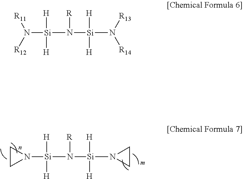
- the bis(aminosilyl)alkylamine compound represented by Chemical Formula 1 may be represented by the following Chemical Formula 6 or 7.
- R is (C1-C7)alkyl or (C2-C7)alkenyl
- R 11 to R 14 are each independently hydrogen, (C1-C7)alkyl, or (C2-C7)alkenyl
- n and m are each independently an integer of 1 to 7.
- R may be (C1-C5)alkyl; R 1 to R 14 may be each independently hydrogen, (C1-C5)alkyl, or (C2-C5)alkenyl; n and m may be each independently an integer of 1 to 4.
- R may be (C1-C5)alkyl; R 11 to R 14 may be each independently (C1-C5)alkyl; and n and m may be each independently 1 to 4.
- the bis(aminosilyl)alkylamine compound may be represented by Chemical Formula 6, wherein in Chemical Formula 6, R may be (C1-C3)alkyl; and R 11 to R 14 may be each independently (C1-C3)alkyl.
- the bis(aminosilyl)alkylamine compound When silyl groups of two aminosilyl groups in the silazane backbone of the bis(aminosilyl)alkylamine compound according to the present disclosure have two or four hydrogen atoms, the bis(aminosilyl)alkylamine compound has more excellent reactivity and thermal stability as the precursor for depositing a thin film, such that a higher-quality thin film may be manufactured.
- the bis(aminosilyl)alkylamine compound represented by Chemical Formula 4 may be represented by the following Chemical Formula 4-1.
- R is (C1-C7)alkyl or (C2-C7)alkenyl
- R 1 and R 2 are each independently hydrogen, (C1-C7)alkyl, or (C2-C7)alkenyl, or R 1 and R 2 is each independently linked to each other to form a ring
- R 5 is (C1-C7)alkyl or (C2-C7)alkenyl.
- the bis(aminosilyl)alkylamine compound represented by Chemical Formula 6 may be represented by the following Chemical Formula 6-1.
- R is (C1-C7)alkyl or (C2-C7)alkenyl; and R 1 and R 2 are each independently (C1-C7)alkyl, or (C2-C7)alkenyl, or are linked to each other to form a ring.)
- bis(aminosilyl)alkylamine compound represented by Chemical Formula 1 may include the following compounds.
- the composition for depositing a silicon-containing thin film according to the present disclosure needs to necessarily contain the bis (amino silyl) alkylamine compound represented by Chemical Formula 1 as the precursor for depositing a thin film, and the bis (amino silyl)alkylamine compound may be contained in the composition for depositing a silicon-containing thin film in a content range in which the content may be recognized by those skilled in the art in consideration of film formation conditions, a thickness, properties, or the like of the thin film.
- alkyl means linear, branched, and cyclic saturated and unsaturated hydrocarbons having 1 to 7 carbon atoms, or 1 to 5 carbon atoms, or 1 to 3 carbon atoms, and examples thereof may include methyl, ethyl, propyl, isopropyl, butyl, isobutyl, neobutyl, pentyl, and the like.
- halogen means a halogen element, and examples thereof include fluoro, chloro, bromo, and iodo.
- alkenyl as a single group or a part of another group means a straight-chain, branched-chain, or cyclic hydrocarbon radical having 2 to 7 carbon atoms and one or more carbon-carbon double bonds.
- a more preferable alkenyl radical is a lower alkenyl radical having 2 to 5 carbon atoms.
- the most preferable lower alkenyl radical is a lower alkenyl radical having about 2 to 3 carbon atoms.
- the alkenyl group may be substituted at a random usable attachment point. Examples of the alkenyl radical include ethenyl, propenyl, allyl, butenyl, and 4-methylbutenyl.
- alkenyl and “lower alkenyl” include radicals having cis and trans orientations or alternatively, E and Z orientations.
- R 1 and R 2 , and R 3 and R 4 are each independently linked to each other to form a ring” includes the case in which R 1 and R 2 are linked to each other to form a ring but R 3 and R 4 do not form a ring; the case in which on the contrary, R 1 and R 2 do not form a ring but R 3 and R 4 are linked to each other to form a ring; and the case in which R 1 and R 2 are linked to each other to form a ring and R 3 and R 4 are linked to each other to form a ring, wherein the formed ring may be an alicyclic or aromatic ring containing N, and, for instance, an alicyclic ring.
- alicyclic ring means a compound that is not an aromatic compound among organic compounds having a cyclic bonding structure.
- the bis(aminosilyl)alkylamine compound represented by Chemical Formula 1 according to the present disclosure may be prepared using a method as long as the method may be recognized by those skilled in the art.
- the present disclosure provides a method for manufacturing a silicon-containing thin film using the composition for depositing a silicon-containing thin film according to the present disclosure.
- the composition for depositing a silicon-containing thin film according to the present disclosure containing the bis(aminosilyl)alkylamine compound represented by Chemical Formula 1, which is a liquid art room temperature and normal pressure and has high volatility and excellent thermal stability, as the precursor is used, the handling may be easy, it is possible to manufacture various thin films, and it is possible to manufacture a silicon-containing thin film having a high purity, an excellent water vapor transmission rate, and excellent thin film stress properties at a high deposition rate even at a low temperature and a low power.
- the silicon-containing thin film manufactured by the method according to the present v has excellent durability and electric properties, and resistance against hydrogen fluoride and step coverage thereof are also excellent.
- the silicon-containing thin film may be formed by any method as long as it may be recognized by those skilled in the art.
- the silicon-containing thin film may be formed by an atomic layer deposition (ALD) method, a chemical vapor deposition (CVD) method, a metal-organic chemical vapor deposition (MOCVD) method, a low-pressure chemical vapor deposition (LPCVD) method, a plasma enhanced chemical vapor deposition (PECVD) method, or a plasma enhanced atomic layer deposition (PEALD) method, but PECVD, ALD, or PEALD may be used in order to allow the thin film to be more easily deposited, and allow the manufactured thin film to have excellent properties.
- ALD atomic layer deposition
- CVD chemical vapor deposition
- MOCVD metal-organic chemical vapor deposition
- LPCVD low-pressure chemical vapor deposition
- PECVD plasma enhanced chemical vapor deposition
- PEALD plasma enhanced atomic layer deposition
- the silicon-containing thin film according to the present disclosure may be a silicon oxide (SiO 2 ) film, a silicon oxy carbide (SiOC) film, a silicon nitride (SiN) film, a silicon oxy nitride (SiON) film, a silicon carbonitride (SiCN) film, or a silicon carbide (SiC) film, and various thin films having high quality, particularly, a thin film usable as an encapsulant of an organic light emitting diode (OLED), may be manufactured.
- SiO 2 silicon oxide
- SiOC silicon oxy carbide
- SiN silicon nitride
- SiON silicon oxy nitride
- SiCN silicon carbonitride
- SiC silicon carbide
- the method for manufacturing a silicon-containing thin film according to the present disclosure may include:
- composition for depositing a silicon-containing thin film according to the present disclosure with the substrate to adsorb the composition for depositing a silicon-containing thin film in the substrate;
- reaction gas in step D) may remove a ligand of the bis(aminosilyl)alkylamine compound contained in the composition for depositing a silicon-containing thin film to form a Si—O atomic layer.
- reaction gas according to the exemplary embodiment of the present disclosure may be supplied after being activated by generating plasma at a plasma power of 50 to 1000 W.
- a bis(aminosilyl)alkylamine compound according to the present disclosure is used as the precursor, such that the reaction gas may be activated at 30 to 500° C., or 30 to 300° C. by generating plasma at a low plasma power of 50 to 1000 W, or 100 to 800 W, or 400 to 600 W, thereby making it possible to manufacture the thin film.
- deposition conditions may be adjusted depending on a structure or thermal properties of a desired thin film.
- the deposition condition according to the exemplary embodiment of the present disclosure may include an injection flow rate of the composition for depositing a silicon-containing thin film containing the bis(aminosilyl)alkyl amine compound, injection flow rates of the reaction gas and a carrier gas, pressure, RF power, the temperature of the substrate, and the like.
- the injection flow rate of the composition for depositing a silicon-containing thin film may be adjusted in a range of 10 to 1000 cc/min
- the injection flow rate of the carrier gas may be adjusted in a range of 10 to 1000 cc/min
- the injection flow rate of the reaction gas may be adjusted in a range of 1 to 1500 cc/min
- the pressure may be adjusted in a range of 0.5 to 10 torr
- the RF power may be adjusted in a range of 50 to 1000 W
- the temperature of the substrate may be adjusted in a range of 30 to 500° C., or 80 to 300° C., but the deposition conditions are not limited thereto.
- the reaction gas used in the method for manufacturing a silicon-containing thin film according to the present disclosure is not limited, but may be one selected from hydrogen (H 2 ), hydrazine (N 2 H 4 ), ozone (O 3 ), oxygen (O 2 ), nitrous oxide (N 2 O) ammonia (NH 3 ), nitrogen (N 2 ), silane (SiH 4 ), borane (BH 3 ), diborane (B 2 H 6 ), and phosphine (PH 3 ), or a mixed gas of one or more thereof, and the carrier gas may be one selected from nitrogen (N 2 ), argon (Ar), and helium (He), or a mixed gas of two or more thereof.
- the substrate used in the method for manufacturing a silicon-containing thin film according to the present disclosure may be a substrate containing one or more semiconductor materials selected from Si, Ge, SiGe, GaP, GaAs, SiC, SiGeC, InAs, and InP; a silicon-on-insulator (SOI) substrate; a quartz substrate; a glass substrate for a display; or a flexible plastic substrate made of polyimide, polyethylene terephthalate (PET), polyethylene naphthalate (PEN), polymethylmethacrylate (PMMA), polycarbonate (PC), polyethersulfone(PES), polyester, and the like, but is not limited thereto.
- SOI silicon-on-insulator
- the silicon-containing thin film may be directly formed on the substrate.
- a large number of conductive layers, dielectric layers, insulating layers, or the like, may also be formed between the substrate and the silicon-containing thin film.
- the present disclosure provides a bis(aminosilyl)alkyl amine compound capable of being used as a precursor of a silicon-containing thin film.
- the bis(aminosilyl)alkyl amine compound according to the present disclosure is represented by the following Chemical Formula 1.
- R is (C1-C7)alkyl or (C2-C7)alkenyl; and R 1 to R 4 are each independently hydrogen, (C1-C7)alkyl, or (C2-C7)alkenyl, or R 1 and R 2 , and R 3 and R 4 are each independently linked to each other to form a ring; and R 5 to R 8 are each independently hydrogen, halogen, (C1-C7)alkyl, or (C2-C7)alkenyl.)
- the bis(aminosilyl)alkyl amine compound according to the present disclosure represented by Chemical Formula 1 is a liquid at room temperature and has high volatility and excellent thermal stability as described above, such that the bis(aminosilyl)alkyl amine compound is used as a significantly useful precursor in forming a silicon-containing thin film.
- the bis(aminosilyl)alkyl amine compound has excellent reactivity, such that the thin film may be deposited at a rapid deposition rate, and the thin film with a high purity may be manufactured.
- the bis(aminosilyl)alkyl amine compound represented by Chemical Formula 1 may be represented by Chemical Formula 2, or Chemical Formula 6 or 7.
- deposition was performed by a plasma enhanced atomic layer deposition (PEALD) method known in the art using a commercialized 200 mm single wafer shower head type ALD apparatus (CN1, Atomic Premium).
- PEALD plasma enhanced atomic layer deposition
- PECVD plasma enhanced chemical vapor deposition
- CN1, Atomic Premium a commercialized 200 mm single wafer shower head type CVD apparatus
- a thickness of a deposited silicon-containing thin film was measured using an ellipsometer (OPTI-PROBE 2600, THERMA-WAVE), and properties of the thin film were analyzed using infrared spectroscopy (IFS66V/S & Hyperion 3000, Bruker Optics), X-ray photoelectron spectroscopy, a water vapor transmission rate (WVTR) analyzer (MOCON, Aquatran 2), and a stress analyzer (Frontier Semiconductor, FSM500TC).
- IFS66V/S & Hyperion 3000 Bruker Optics
- WVTR water vapor transmission rate
- FSM500TC Frier Semiconductor
- Film was formed using the bis(ethylmethylaminosilyl)methyl amine compound prepared in Example 2 according to the present disclosure as a composition for forming a silicon oxide film in a general plasma enhanced atomic layer deposition (PEALD) apparatus using a plasma enhanced atomic layer deposition (PEALD) method known in the art.
- PEALD plasma enhanced atomic layer deposition
- nitrous oxide was used together with plasma, and nitrogen corresponding to an inert gas was used for purging.
- the film was formed at reaction gas and plasma time of 0.5 seconds.
- a specific method for depositing a silicon oxide thin film was illustrated in Table 1.
- Silicon oxide thin films were manufactured in the same manner as in Example 3 except for changing deposition conditions illustrated in the following Table 1 in Example 3, results obtained by analyzing the manufactured silicon oxide thin film were illustrated in the following Table 2, and results obtained by analyzing the deposited film using the infrared spectroscopy were illustrated in FIG. 3 .
- Film was formed using the bis(ethylmethylaminosilyl)methyl amine compound prepared in Example 2 according to the present disclosure as a composition for forming a silicon nitride film in a general plasma enhanced atomic layer deposition (PEALD) apparatus using a plasma enhanced atomic layer deposition (PEALD) method known in the art.
- PEALD plasma enhanced atomic layer deposition
- As a reaction gas nitrogen and ammonia were used together with plasma as first reaction gas, and nitrogen was used as a second reaction gas. The nitrogen corresponding to an inert gas was used for purging.
- a specific method for depositing a silicon nitride thin film was illustrated in Table 3.
- Silicon nitride thin films were manufactured in the same manner as in Example 6 except for changing conditions illustrated in the following Table 3 in Example 6, results obtained by analyzing the manufactured silicon oxide thin film were illustrated in the following Table 4, and results obtained by analyzing the deposited film using the infrared spectrometer were illustrated in FIG. 4 .
Landscapes
- Chemical & Material Sciences (AREA)
- Engineering & Computer Science (AREA)
- Organic Chemistry (AREA)
- Chemical Kinetics & Catalysis (AREA)
- Physics & Mathematics (AREA)
- Materials Engineering (AREA)
- General Chemical & Material Sciences (AREA)
- Mechanical Engineering (AREA)
- Metallurgy (AREA)
- Inorganic Chemistry (AREA)
- Computer Hardware Design (AREA)
- Manufacturing & Machinery (AREA)
- General Physics & Mathematics (AREA)
- Power Engineering (AREA)
- Microelectronics & Electronic Packaging (AREA)
- Condensed Matter Physics & Semiconductors (AREA)
- Plasma & Fusion (AREA)
- Life Sciences & Earth Sciences (AREA)
- Wood Science & Technology (AREA)
- Electromagnetism (AREA)
- Chemical Vapour Deposition (AREA)
- Formation Of Insulating Films (AREA)
Abstract
Description


| TABLE 1 |
| Deposition Conditions of Silicon Oxide Thin Film by PEALD |
| Precursor | Purge | Reaction Gas and Plasma | No. of Deposition |
| Temperature | Heating | Injection | Flow | Flow | RF | Reaction Gas Purge | Flow | Process |
| of Substrate | Temperature | Time | Rate | Time | Rate | Power | Time | Time | Rate | Time | ||
| (° C.) | (° C.) | (sec) | (sccm) | (sec) | (sccm) | (W) | (sec) | (sec) | (sccm) | Cycle | (sec) | |
| Example 3 | 90 | 65 | 0.1 | 600 | 0.4 | 800 | 400 | 0.5 | 0.1 | 300 | 614 | 675 |
| Example 4 | 90 | 65 | 0.1 | 600 | 0.4 | 800 | 400 | 0.7 | 0.1 | 300 | 603 | 784 |
| Example 5 | 90 | 65 | 0.1 | 600 | 0.4 | 800 | 400 | 0.9 | 0.1 | 300 | 603 | 905 |
| TABLE 2 |
| Evaluation of Properties of Silicon Oxide Thin Film |
| O/Si | ||||||
| Deposition | Thickness of | Refractive | Composition | Stress | ||
| Rate | Thin Film | Index | Ratio | of Film | WVTR | |
| (Å/cycle) | (Å) | — | — | (MPa) | (g/[m2-day]) | |
| Example 3 | 1.14 | 700 | 1.46 | 1.72 | −201 | 3.2E−02 |
| Example 4 | 1.16 | 700 | 1.47 | 1.72 | −231 | 1.5E−02 |
| Example 5 | 1.16 | 700 | 1.47 | 1.72 | −275 | 3.5E−03 |
| TABLE 3 |
| Deposition Conditions of Silicon Nitride Thin Film by PEALD |
| Precursor | Purge | Reaction Gas and Plasma |
| Temperature | Heating | Injection | Flow | Flow | RF | |||
| of Substrate | Temperature | Time | Rate | Time | Rate | Power | Time | |
| (° C.) | (° C.) | (sec) | (sccm) | (sec) | (sccm) | (W) | (sec) | |
| Example 6 | 300 | 65 | 0.4 | 6000 | 0.4 | 2000 | 100 | 1.5 |
| Example 7 | 300 | 65 | 0.4 | 6000 | 0.4 | 2000 | 200 | 1.5 |
| Example 8 | 300 | 65 | 0.4 | 6000 | 0.4 | 2000 | 400 | 1.5 |
| Example 9 | 300 | 65 | 0.4 | 6000 | 0.4 | 2000 | 800 | 1.5 |
| Reaction Gas and Plasma | Reaction Gas Purge |
| Flow | RF | Flow | No. of | Process | ||||
| Rate | Power | Time | Time | Rate | Deposition | Time | ||
| (sccm) | (W) | (sec) | (sec) | (sccm) | Cycle | (sec) | ||
| Example 6 | 6000 | 600 | 4 | 0.4 | 6000 | 300 | 2130 | |
| Example 7 | 6000 | 600 | 4 | 0.4 | 6000 | 300 | 2130 | |
| Example 8 | 6000 | 600 | 4 | 0.4 | 6000 | 300 | 2130 | |
| Example 9 | 6000 | 600 | 4 | 0.4 | 6000 | 300 | 2130 | |
| TABLE 4 |
| Evaluation of Properties of Silicon Nitride Thin Film |
| Deposition | Thickness of | Refractive | N/Si | Stress | |||
| Rate | Thin Film | Index | Composition | of Film | WVTR | ||
| Variable | (Å/cycle) | (Å) | — | Ratio | (MPa) | (g/[m2-day]) | |
| Example 6 | Plasma Power | 0.29 | 88 | 1.93 | 1.13 | −301 | 6.2E−02 |
| of 100 W | |||||||
| Example 7 | Plasma Power | 0.22 | 67 | 1.89 | 1.16 | −350 | 1.1E−02 |
| of 200 W | |||||||
| Example 8 | Plasma Power | 0.34 | 103 | 1.95 | 1.18 | −416 | 3.5E−03 |
| of 400 W | |||||||
| Example 9 | Plasma Power | 0.38 | 114 | 1.80 | 1.21 | −517 | 5.3E−03 |
| of 800 W | |||||||
Claims (7)


Priority Applications (1)
| Application Number | Priority Date | Filing Date | Title |
|---|---|---|---|
| US17/572,509 US11749522B2 (en) | 2017-03-29 | 2022-01-10 | Composition for depositing silicon-containing thin film containing bis(aminosilyl)alkylamine compound and method for manufacturing silicon-containing thin using the same |
Applications Claiming Priority (9)
| Application Number | Priority Date | Filing Date | Title |
|---|---|---|---|
| KR10-2017-0040078 | 2017-03-29 | ||
| KR20170040078 | 2017-03-29 | ||
| KR10-2017-0055632 | 2017-04-28 | ||
| KR20170055632 | 2017-04-28 | ||
| KR1020180035010A KR20180110612A (en) | 2017-03-29 | 2018-03-27 | Compositions for depositing silicon-containing thin films containing bis(aminosilyl)alkylamine compound and methods for manufacturing silicon-containing thin film using the same |
| KR10-2018-0035010 | 2018-03-27 | ||
| PCT/KR2018/003655 WO2018182309A1 (en) | 2017-03-29 | 2018-03-28 | Composition for depositing silicon-containing thin film containing bis(aminosilyl)alkylamine compound and method for manufacturing silicon-containing thin film using the same |
| US201916499215A | 2019-09-27 | 2019-09-27 | |
| US17/572,509 US11749522B2 (en) | 2017-03-29 | 2022-01-10 | Composition for depositing silicon-containing thin film containing bis(aminosilyl)alkylamine compound and method for manufacturing silicon-containing thin using the same |
Related Parent Applications (2)
| Application Number | Title | Priority Date | Filing Date |
|---|---|---|---|
| US16/499,215 Continuation US11393676B2 (en) | 2017-03-29 | 2018-03-28 | Composition for depositing silicon-containing thin film containing bis(aminosilyl)alkylamine compound and method for manufacturing silicon-containing thin film using the same |
| PCT/KR2018/003655 Continuation WO2018182309A1 (en) | 2017-03-29 | 2018-03-28 | Composition for depositing silicon-containing thin film containing bis(aminosilyl)alkylamine compound and method for manufacturing silicon-containing thin film using the same |
Publications (2)
| Publication Number | Publication Date |
|---|---|
| US20220139704A1 US20220139704A1 (en) | 2022-05-05 |
| US11749522B2 true US11749522B2 (en) | 2023-09-05 |
Family
ID=63876104
Family Applications (2)
| Application Number | Title | Priority Date | Filing Date |
|---|---|---|---|
| US16/499,215 Active 2038-10-08 US11393676B2 (en) | 2017-03-29 | 2018-03-28 | Composition for depositing silicon-containing thin film containing bis(aminosilyl)alkylamine compound and method for manufacturing silicon-containing thin film using the same |
| US17/572,509 Active US11749522B2 (en) | 2017-03-29 | 2022-01-10 | Composition for depositing silicon-containing thin film containing bis(aminosilyl)alkylamine compound and method for manufacturing silicon-containing thin using the same |
Family Applications Before (1)
| Application Number | Title | Priority Date | Filing Date |
|---|---|---|---|
| US16/499,215 Active 2038-10-08 US11393676B2 (en) | 2017-03-29 | 2018-03-28 | Composition for depositing silicon-containing thin film containing bis(aminosilyl)alkylamine compound and method for manufacturing silicon-containing thin film using the same |
Country Status (5)
| Country | Link |
|---|---|
| US (2) | US11393676B2 (en) |
| JP (1) | JP6876145B2 (en) |
| KR (3) | KR20180110612A (en) |
| CN (1) | CN110431204B (en) |
| TW (1) | TWI705970B (en) |
Families Citing this family (7)
| Publication number | Priority date | Publication date | Assignee | Title |
|---|---|---|---|---|
| KR102093227B1 (en) * | 2017-04-20 | 2020-03-25 | (주)디엔에프 | Disilyl amine compound, method for preparing the same and composition for depositing silicon-containing thin film containing the same |
| KR20210037393A (en) * | 2019-09-27 | 2021-04-06 | (주)덕산테코피아 | Amino-silane compound and composition for the silicon-containing thin film comprising it |
| CN111925799B (en) * | 2020-08-14 | 2021-10-01 | 上海新阳半导体材料股份有限公司 | A kind of high selectivity ratio etching solution, its preparation method and application |
| CN111961472B (en) * | 2020-08-14 | 2022-06-21 | 上海新阳半导体材料股份有限公司 | High-selectivity silicon nitride etching solution, and preparation method and application thereof |
| KR102723766B1 (en) * | 2022-04-25 | 2024-10-31 | 메르크 파텐트 게엠베하 | Silicon precursor compounds and method for manufacturing the same, and method of forming silicon-containing films |
| WO2024225770A1 (en) * | 2023-04-27 | 2024-10-31 | (주)디엔에프 | Fluorodisilazane compound, composition comprising same for depositing silicon-containing thin film, and method for manufacturing silicon-containing thin film using same |
| KR20250014292A (en) * | 2023-07-19 | 2025-02-03 | 메르크 파텐트 게엠베하 | Silicon precursor compounds and method for manufacturing the same, and method of forming silicon-containing films |
Citations (12)
| Publication number | Priority date | Publication date | Assignee | Title |
|---|---|---|---|---|
| JP2008074847A (en) | 2006-09-01 | 2008-04-03 | Air Products & Chemicals Inc | Stabilization of ntirogen-containing and oxygen-containing organosilanes using weakly basic ion-exchange resin |
| WO2008038255A1 (en) | 2006-09-29 | 2008-04-03 | L'air Liquide-Societe Anonyme Pour L'etude Et L'exploitation Des Procedes Georges Claude | Silicon precursors and method for low temperature cvd of silicon-containing films |
| US20090095346A1 (en) | 2007-10-12 | 2009-04-16 | Air Products And Chemicals, Inc. | Antireflective coatings for photovoltaic applications |
| CN103401019A (en) | 2013-08-08 | 2013-11-20 | 东莞市杉杉电池材料有限公司 | Silazane additive and lithium ion battery electrolyte prepared by using same and capable of preventing corrosion of steel shell |
| EP2669249A1 (en) | 2012-06-01 | 2013-12-04 | Air Products And Chemicals, Inc. | Organoaminodisilane precursors and methods for depositing films comprising same |
| JP2014523638A (en) | 2011-06-03 | 2014-09-11 | エア プロダクツ アンド ケミカルズ インコーポレイテッド | Compositions and methods for depositing carbon-doped silicon-containing films |
| WO2014196827A2 (en) | 2013-06-07 | 2014-12-11 | Dnf Co., Ltd. | Novel amino-silyl amine compound, method for perparing the 'same and silicon-containing thin-film using the same |
| KR20140143682A (en) | 2013-06-07 | 2014-12-17 | (주)디엔에프 | Novel amino-silyl amine compound, method for manufacturing thereof and silicon-containing thin film use the same |
| JP2014237644A (en) | 2013-06-07 | 2014-12-18 | ディーエヌエフ カンパニー リミテッドDNF Co. Ltd. | New amino silyl amine compound, production method thereof, and silicon-containing thin film using the same |
| CN105377860A (en) | 2013-06-07 | 2016-03-02 | Dnf有限公司 | Novel amino-silyl amine compound, method for perparing the 'same and silicon-containing thin-film using the same |
| WO2016049154A1 (en) | 2014-09-23 | 2016-03-31 | L'air Liquide, Societe Anonyme Pour L'etude Et L'exploitation Des Procedes Georges Claude | Carbosilane substituted amine precursors for deposition of si-containing films and methods thereof |
| US20160280724A1 (en) | 2015-03-23 | 2016-09-29 | Gelest Technologies, Inc. | N-alkyl substituted cyclic and oligomeric perhydridosilazanes, methods of preparation thereof, and silicon nitride films formed therefrom |
Family Cites Families (10)
| Publication number | Priority date | Publication date | Assignee | Title |
|---|---|---|---|---|
| FR2599037B1 (en) * | 1986-05-26 | 1990-05-04 | Europ Propulsion | DIHYDROGENO-1,3 FUNCTIONAL DISILAZANES AND PROCESS FOR THEIR PREPARATION |
| JP2920159B2 (en) * | 1989-09-30 | 1999-07-19 | 東燃株式会社 | Composition for coating |
| US6071830A (en) | 1996-04-17 | 2000-06-06 | Sony Corporation | Method of forming insulating film |
| JP3709891B1 (en) * | 2005-01-07 | 2005-10-26 | 東陶機器株式会社 | COMPOSITE MATERIAL, COATING LIQUID AND METHOD FOR PRODUCING COMPOSITE MATERIAL |
| US20090075490A1 (en) * | 2007-09-18 | 2009-03-19 | L'air Liquite Societe Anonyme Pour L'etude Et L'exploitation Des Procedes Georges Claude | Method of forming silicon-containing films |
| KR20140059107A (en) * | 2012-11-07 | 2014-05-15 | 주식회사 유피케미칼 | Method for forming silicon nitride thin film |
| CN103396738A (en) * | 2013-06-24 | 2013-11-20 | 中国电子科技集团公司第十研究所 | Preparation method of semi-inorganic heat-insulating and wave-permeable coating material |
| JP6071830B2 (en) | 2013-09-25 | 2017-02-01 | 本田技研工業株式会社 | Body |
| KR101875183B1 (en) * | 2014-06-11 | 2018-07-06 | (주)디엔에프 | Novel amino-silyl amine compound and the manufacturing method of dielectric film containing Si-N bond by using atomic layer deposition |
| KR101718744B1 (en) * | 2014-11-03 | 2017-03-23 | (주)디엔에프 | Composition containing silicon precursor for thin film deposition and a silicon-containing thin film manufactured thereof |
-
2018
- 2018-03-27 KR KR1020180035010A patent/KR20180110612A/en not_active Ceased
- 2018-03-28 JP JP2019553053A patent/JP6876145B2/en active Active
- 2018-03-28 CN CN201880019422.XA patent/CN110431204B/en active Active
- 2018-03-28 TW TW107110762A patent/TWI705970B/en active
- 2018-03-28 US US16/499,215 patent/US11393676B2/en active Active
-
2020
- 2020-07-09 KR KR1020200084525A patent/KR102166730B1/en active Active
- 2020-07-09 KR KR1020200084528A patent/KR102217645B1/en active Active
-
2022
- 2022-01-10 US US17/572,509 patent/US11749522B2/en active Active
Patent Citations (13)
| Publication number | Priority date | Publication date | Assignee | Title |
|---|---|---|---|---|
| JP2008074847A (en) | 2006-09-01 | 2008-04-03 | Air Products & Chemicals Inc | Stabilization of ntirogen-containing and oxygen-containing organosilanes using weakly basic ion-exchange resin |
| WO2008038255A1 (en) | 2006-09-29 | 2008-04-03 | L'air Liquide-Societe Anonyme Pour L'etude Et L'exploitation Des Procedes Georges Claude | Silicon precursors and method for low temperature cvd of silicon-containing films |
| US20090095346A1 (en) | 2007-10-12 | 2009-04-16 | Air Products And Chemicals, Inc. | Antireflective coatings for photovoltaic applications |
| US20140287164A1 (en) * | 2011-06-03 | 2014-09-25 | Air Products And Chemicals, Inc. | Compositions and processes for depositing carbon-doped silicon-containing films |
| JP2014523638A (en) | 2011-06-03 | 2014-09-11 | エア プロダクツ アンド ケミカルズ インコーポレイテッド | Compositions and methods for depositing carbon-doped silicon-containing films |
| EP2669249A1 (en) | 2012-06-01 | 2013-12-04 | Air Products And Chemicals, Inc. | Organoaminodisilane precursors and methods for depositing films comprising same |
| JP2014237644A (en) | 2013-06-07 | 2014-12-18 | ディーエヌエフ カンパニー リミテッドDNF Co. Ltd. | New amino silyl amine compound, production method thereof, and silicon-containing thin film using the same |
| WO2014196827A2 (en) | 2013-06-07 | 2014-12-11 | Dnf Co., Ltd. | Novel amino-silyl amine compound, method for perparing the 'same and silicon-containing thin-film using the same |
| KR20140143682A (en) | 2013-06-07 | 2014-12-17 | (주)디엔에프 | Novel amino-silyl amine compound, method for manufacturing thereof and silicon-containing thin film use the same |
| CN105377860A (en) | 2013-06-07 | 2016-03-02 | Dnf有限公司 | Novel amino-silyl amine compound, method for perparing the 'same and silicon-containing thin-film using the same |
| CN103401019A (en) | 2013-08-08 | 2013-11-20 | 东莞市杉杉电池材料有限公司 | Silazane additive and lithium ion battery electrolyte prepared by using same and capable of preventing corrosion of steel shell |
| WO2016049154A1 (en) | 2014-09-23 | 2016-03-31 | L'air Liquide, Societe Anonyme Pour L'etude Et L'exploitation Des Procedes Georges Claude | Carbosilane substituted amine precursors for deposition of si-containing films and methods thereof |
| US20160280724A1 (en) | 2015-03-23 | 2016-09-29 | Gelest Technologies, Inc. | N-alkyl substituted cyclic and oligomeric perhydridosilazanes, methods of preparation thereof, and silicon nitride films formed therefrom |
Non-Patent Citations (6)
| Title |
|---|
| "CAS No. 23636-57-9," ichemistry Website, Available Online at http://www.ichemistry.cn/chemistry/23636-57-9.htm. Retrieved on Dec. 1, 2021, 3 pages. (See NPL 1, Office Action Issued in U.S. Appl. No. 16/499,196 for Explanation of Relevancy). |
| Freza, S. et al., "Influence of substituents in vinyl groups on reactivity of parylene during polymerization process," Chemical Physics, vol. 368, No. 3, Mar. 11, 2010, Available Online Jan. 28, 2010, 7 pages. |
| ISA Korean Intellectual Property Office, International Search Report Issued in Application No. PCT/KR2018/003655, dated Jul. 13, 2018, WIPO, 2 pages. |
| Japanese Patent Office, Office Action Issued in Application No. 2019-553053, dated Nov. 27, 2020, 9 pages. |
| State Intellectual Property Office of the People's Republic of China, Office Action and Search Report Issued in Application No. 201880019422.X, dated Nov. 13, 2020, 13 pages (Submitted with Partial Translation). |
| United States Patent and Trademark Office, Office Action Issued in U.S. Appl. No. 16/499,196, dated May 24, 2021, 19 pages. |
Also Published As
| Publication number | Publication date |
|---|---|
| TWI705970B (en) | 2020-10-01 |
| TW201900658A (en) | 2019-01-01 |
| US20220139704A1 (en) | 2022-05-05 |
| KR20180110612A (en) | 2018-10-10 |
| US20200111664A1 (en) | 2020-04-09 |
| CN110431204B (en) | 2021-06-18 |
| US11393676B2 (en) | 2022-07-19 |
| CN110431204A (en) | 2019-11-08 |
| KR20200090653A (en) | 2020-07-29 |
| JP6876145B2 (en) | 2021-05-26 |
| JP2020516067A (en) | 2020-05-28 |
| KR102217645B1 (en) | 2021-02-19 |
| KR102166730B1 (en) | 2020-10-16 |
| KR20200090654A (en) | 2020-07-29 |
Similar Documents
| Publication | Publication Date | Title |
|---|---|---|
| US11749522B2 (en) | Composition for depositing silicon-containing thin film containing bis(aminosilyl)alkylamine compound and method for manufacturing silicon-containing thin using the same | |
| US11358974B2 (en) | Silylamine compound, composition for depositing silicon-containing thin film containing the same, and method for manufacturing silicon-containing thin film using the composition | |
| TWI496934B (en) | Compositions and processes for depositing carbon-doped silicon-containing films | |
| KR102190532B1 (en) | Composition for silicon-containing thin films and method for producing silicon-containing thin film | |
| US11319333B2 (en) | Disilylamine compound, method for preparing the same, and composition for depositing silicon-containing thin film including the same | |
| US20230089296A1 (en) | Composition for depositing silicon-containing thin film and method for manufacturing silicon-containing thin film using the same | |
| US10894799B2 (en) | Composition for depositing silicon-containing thin film including disilylamine compound and method for manufacturing silicon-containing thin film using the same | |
| US12304924B2 (en) | Silylcyclodisilazane compound and method for manufacturing silicon-containing thin film using the same |
Legal Events
| Date | Code | Title | Description |
|---|---|---|---|
| AS | Assignment |
Owner name: DNF CO., LTD., KOREA, REPUBLIC OF Free format text: ASSIGNMENT OF ASSIGNORS INTEREST;ASSIGNORS:KIM, SUNG GI;PARK, JEONG JOO;PARK, JOONG JIN;AND OTHERS;REEL/FRAME:058685/0612 Effective date: 20190910 |
|
| FEPP | Fee payment procedure |
Free format text: ENTITY STATUS SET TO UNDISCOUNTED (ORIGINAL EVENT CODE: BIG.); ENTITY STATUS OF PATENT OWNER: SMALL ENTITY |
|
| FEPP | Fee payment procedure |
Free format text: ENTITY STATUS SET TO SMALL (ORIGINAL EVENT CODE: SMAL); ENTITY STATUS OF PATENT OWNER: SMALL ENTITY |
|
| STPP | Information on status: patent application and granting procedure in general |
Free format text: DOCKETED NEW CASE - READY FOR EXAMINATION |
|
| STPP | Information on status: patent application and granting procedure in general |
Free format text: NOTICE OF ALLOWANCE MAILED -- APPLICATION RECEIVED IN OFFICE OF PUBLICATIONS |
|
| STPP | Information on status: patent application and granting procedure in general |
Free format text: NOTICE OF ALLOWANCE MAILED -- APPLICATION RECEIVED IN OFFICE OF PUBLICATIONS |
|
| STCF | Information on status: patent grant |
Free format text: PATENTED CASE |