US11735683B1 - Single-crystal beta-Ga2O3 MSM detector and preparation method thereof - Google Patents
Single-crystal beta-Ga2O3 MSM detector and preparation method thereof Download PDFInfo
- Publication number
- US11735683B1 US11735683B1 US18/169,552 US202318169552A US11735683B1 US 11735683 B1 US11735683 B1 US 11735683B1 US 202318169552 A US202318169552 A US 202318169552A US 11735683 B1 US11735683 B1 US 11735683B1
- Authority
- US
- United States
- Prior art keywords
- crystal
- substrate
- waterjet
- laser
- preparing
- Prior art date
- Legal status (The legal status is an assumption and is not a legal conclusion. Google has not performed a legal analysis and makes no representation as to the accuracy of the status listed.)
- Active
Links
Images


Classifications
-
- C—CHEMISTRY; METALLURGY
- C01—INORGANIC CHEMISTRY
- C01G—COMPOUNDS CONTAINING METALS NOT COVERED BY SUBCLASSES C01D OR C01F
- C01G15/00—Compounds of gallium, indium or thallium
-
- H01L31/18—
-
- B—PERFORMING OPERATIONS; TRANSPORTING
- B08—CLEANING
- B08B—CLEANING IN GENERAL; PREVENTION OF FOULING IN GENERAL
- B08B3/00—Cleaning by methods involving the use or presence of liquid or steam
- B08B3/02—Cleaning by the force of jets or sprays
-
- B—PERFORMING OPERATIONS; TRANSPORTING
- B23—MACHINE TOOLS; METAL-WORKING NOT OTHERWISE PROVIDED FOR
- B23K—SOLDERING OR UNSOLDERING; WELDING; CLADDING OR PLATING BY SOLDERING OR WELDING; CUTTING BY APPLYING HEAT LOCALLY, e.g. FLAME CUTTING; WORKING BY LASER BEAM
- B23K26/00—Working by laser beam, e.g. welding, cutting or boring
- B23K26/352—Working by laser beam, e.g. welding, cutting or boring for surface treatment
- B23K26/354—Working by laser beam, e.g. welding, cutting or boring for surface treatment by melting
-
- C—CHEMISTRY; METALLURGY
- C23—COATING METALLIC MATERIAL; COATING MATERIAL WITH METALLIC MATERIAL; CHEMICAL SURFACE TREATMENT; DIFFUSION TREATMENT OF METALLIC MATERIAL; COATING BY VACUUM EVAPORATION, BY SPUTTERING, BY ION IMPLANTATION OR BY CHEMICAL VAPOUR DEPOSITION, IN GENERAL; INHIBITING CORROSION OF METALLIC MATERIAL OR INCRUSTATION IN GENERAL
- C23C—COATING METALLIC MATERIAL; COATING MATERIAL WITH METALLIC MATERIAL; SURFACE TREATMENT OF METALLIC MATERIAL BY DIFFUSION INTO THE SURFACE, BY CHEMICAL CONVERSION OR SUBSTITUTION; COATING BY VACUUM EVAPORATION, BY SPUTTERING, BY ION IMPLANTATION OR BY CHEMICAL VAPOUR DEPOSITION, IN GENERAL
- C23C14/00—Coating by vacuum evaporation, by sputtering or by ion implantation of the coating forming material
- C23C14/02—Pretreatment of the material to be coated
- C23C14/021—Cleaning or etching treatments
- C23C14/022—Cleaning or etching treatments by means of bombardment with energetic particles or radiation
-
- C—CHEMISTRY; METALLURGY
- C23—COATING METALLIC MATERIAL; COATING MATERIAL WITH METALLIC MATERIAL; CHEMICAL SURFACE TREATMENT; DIFFUSION TREATMENT OF METALLIC MATERIAL; COATING BY VACUUM EVAPORATION, BY SPUTTERING, BY ION IMPLANTATION OR BY CHEMICAL VAPOUR DEPOSITION, IN GENERAL; INHIBITING CORROSION OF METALLIC MATERIAL OR INCRUSTATION IN GENERAL
- C23C—COATING METALLIC MATERIAL; COATING MATERIAL WITH METALLIC MATERIAL; SURFACE TREATMENT OF METALLIC MATERIAL BY DIFFUSION INTO THE SURFACE, BY CHEMICAL CONVERSION OR SUBSTITUTION; COATING BY VACUUM EVAPORATION, BY SPUTTERING, BY ION IMPLANTATION OR BY CHEMICAL VAPOUR DEPOSITION, IN GENERAL
- C23C14/00—Coating by vacuum evaporation, by sputtering or by ion implantation of the coating forming material
- C23C14/02—Pretreatment of the material to be coated
- C23C14/028—Physical treatment to alter the texture of the substrate surface, e.g. grinding, polishing
-
- C—CHEMISTRY; METALLURGY
- C23—COATING METALLIC MATERIAL; COATING MATERIAL WITH METALLIC MATERIAL; CHEMICAL SURFACE TREATMENT; DIFFUSION TREATMENT OF METALLIC MATERIAL; COATING BY VACUUM EVAPORATION, BY SPUTTERING, BY ION IMPLANTATION OR BY CHEMICAL VAPOUR DEPOSITION, IN GENERAL; INHIBITING CORROSION OF METALLIC MATERIAL OR INCRUSTATION IN GENERAL
- C23C—COATING METALLIC MATERIAL; COATING MATERIAL WITH METALLIC MATERIAL; SURFACE TREATMENT OF METALLIC MATERIAL BY DIFFUSION INTO THE SURFACE, BY CHEMICAL CONVERSION OR SUBSTITUTION; COATING BY VACUUM EVAPORATION, BY SPUTTERING, BY ION IMPLANTATION OR BY CHEMICAL VAPOUR DEPOSITION, IN GENERAL
- C23C14/00—Coating by vacuum evaporation, by sputtering or by ion implantation of the coating forming material
- C23C14/06—Coating by vacuum evaporation, by sputtering or by ion implantation of the coating forming material characterised by the coating material
- C23C14/14—Metallic material, boron or silicon
- C23C14/18—Metallic material, boron or silicon on other inorganic substrates
-
- C—CHEMISTRY; METALLURGY
- C23—COATING METALLIC MATERIAL; COATING MATERIAL WITH METALLIC MATERIAL; CHEMICAL SURFACE TREATMENT; DIFFUSION TREATMENT OF METALLIC MATERIAL; COATING BY VACUUM EVAPORATION, BY SPUTTERING, BY ION IMPLANTATION OR BY CHEMICAL VAPOUR DEPOSITION, IN GENERAL; INHIBITING CORROSION OF METALLIC MATERIAL OR INCRUSTATION IN GENERAL
- C23C—COATING METALLIC MATERIAL; COATING MATERIAL WITH METALLIC MATERIAL; SURFACE TREATMENT OF METALLIC MATERIAL BY DIFFUSION INTO THE SURFACE, BY CHEMICAL CONVERSION OR SUBSTITUTION; COATING BY VACUUM EVAPORATION, BY SPUTTERING, BY ION IMPLANTATION OR BY CHEMICAL VAPOUR DEPOSITION, IN GENERAL
- C23C14/00—Coating by vacuum evaporation, by sputtering or by ion implantation of the coating forming material
- C23C14/22—Coating by vacuum evaporation, by sputtering or by ion implantation of the coating forming material characterised by the process of coating
- C23C14/24—Vacuum evaporation
-
- C—CHEMISTRY; METALLURGY
- C30—CRYSTAL GROWTH
- C30B—SINGLE-CRYSTAL GROWTH; UNIDIRECTIONAL SOLIDIFICATION OF EUTECTIC MATERIAL OR UNIDIRECTIONAL DEMIXING OF EUTECTOID MATERIAL; REFINING BY ZONE-MELTING OF MATERIAL; PRODUCTION OF A HOMOGENEOUS POLYCRYSTALLINE MATERIAL WITH DEFINED STRUCTURE; SINGLE CRYSTALS OR HOMOGENEOUS POLYCRYSTALLINE MATERIAL WITH DEFINED STRUCTURE; AFTER-TREATMENT OF SINGLE CRYSTALS OR A HOMOGENEOUS POLYCRYSTALLINE MATERIAL WITH DEFINED STRUCTURE; APPARATUS THEREFOR
- C30B29/00—Single crystals or homogeneous polycrystalline material with defined structure characterised by the material or by their shape
- C30B29/10—Inorganic compounds or compositions
- C30B29/16—Oxides
-
- C—CHEMISTRY; METALLURGY
- C30—CRYSTAL GROWTH
- C30B—SINGLE-CRYSTAL GROWTH; UNIDIRECTIONAL SOLIDIFICATION OF EUTECTIC MATERIAL OR UNIDIRECTIONAL DEMIXING OF EUTECTOID MATERIAL; REFINING BY ZONE-MELTING OF MATERIAL; PRODUCTION OF A HOMOGENEOUS POLYCRYSTALLINE MATERIAL WITH DEFINED STRUCTURE; SINGLE CRYSTALS OR HOMOGENEOUS POLYCRYSTALLINE MATERIAL WITH DEFINED STRUCTURE; AFTER-TREATMENT OF SINGLE CRYSTALS OR A HOMOGENEOUS POLYCRYSTALLINE MATERIAL WITH DEFINED STRUCTURE; APPARATUS THEREFOR
- C30B33/00—After-treatment of single crystals or homogeneous polycrystalline material with defined structure
- C30B33/04—After-treatment of single crystals or homogeneous polycrystalline material with defined structure using electric or magnetic fields or particle radiation
-
- C—CHEMISTRY; METALLURGY
- C30—CRYSTAL GROWTH
- C30B—SINGLE-CRYSTAL GROWTH; UNIDIRECTIONAL SOLIDIFICATION OF EUTECTIC MATERIAL OR UNIDIRECTIONAL DEMIXING OF EUTECTOID MATERIAL; REFINING BY ZONE-MELTING OF MATERIAL; PRODUCTION OF A HOMOGENEOUS POLYCRYSTALLINE MATERIAL WITH DEFINED STRUCTURE; SINGLE CRYSTALS OR HOMOGENEOUS POLYCRYSTALLINE MATERIAL WITH DEFINED STRUCTURE; AFTER-TREATMENT OF SINGLE CRYSTALS OR A HOMOGENEOUS POLYCRYSTALLINE MATERIAL WITH DEFINED STRUCTURE; APPARATUS THEREFOR
- C30B33/00—After-treatment of single crystals or homogeneous polycrystalline material with defined structure
- C30B33/08—Etching
- C30B33/10—Etching in solutions or melts
-
- H01L31/022408—
-
- H01L31/1085—
-
- H—ELECTRICITY
- H10—SEMICONDUCTOR DEVICES; ELECTRIC SOLID-STATE DEVICES NOT OTHERWISE PROVIDED FOR
- H10F—INORGANIC SEMICONDUCTOR DEVICES SENSITIVE TO INFRARED RADIATION, LIGHT, ELECTROMAGNETIC RADIATION OF SHORTER WAVELENGTH OR CORPUSCULAR RADIATION
- H10F30/00—Individual radiation-sensitive semiconductor devices in which radiation controls the flow of current through the devices, e.g. photodetectors
- H10F30/10—Individual radiation-sensitive semiconductor devices in which radiation controls the flow of current through the devices, e.g. photodetectors the devices being sensitive to infrared radiation, visible or ultraviolet radiation, and having no potential barriers, e.g. photoresistors
-
- H—ELECTRICITY
- H10—SEMICONDUCTOR DEVICES; ELECTRIC SOLID-STATE DEVICES NOT OTHERWISE PROVIDED FOR
- H10F—INORGANIC SEMICONDUCTOR DEVICES SENSITIVE TO INFRARED RADIATION, LIGHT, ELECTROMAGNETIC RADIATION OF SHORTER WAVELENGTH OR CORPUSCULAR RADIATION
- H10F30/00—Individual radiation-sensitive semiconductor devices in which radiation controls the flow of current through the devices, e.g. photodetectors
- H10F30/20—Individual radiation-sensitive semiconductor devices in which radiation controls the flow of current through the devices, e.g. photodetectors the devices having potential barriers, e.g. phototransistors
- H10F30/21—Individual radiation-sensitive semiconductor devices in which radiation controls the flow of current through the devices, e.g. photodetectors the devices having potential barriers, e.g. phototransistors the devices being sensitive to infrared, visible or ultraviolet radiation
- H10F30/22—Individual radiation-sensitive semiconductor devices in which radiation controls the flow of current through the devices, e.g. photodetectors the devices having potential barriers, e.g. phototransistors the devices being sensitive to infrared, visible or ultraviolet radiation the devices having only one potential barrier, e.g. photodiodes
- H10F30/227—Individual radiation-sensitive semiconductor devices in which radiation controls the flow of current through the devices, e.g. photodetectors the devices having potential barriers, e.g. phototransistors the devices being sensitive to infrared, visible or ultraviolet radiation the devices having only one potential barrier, e.g. photodiodes the potential barrier being a Schottky barrier
- H10F30/2275—Individual radiation-sensitive semiconductor devices in which radiation controls the flow of current through the devices, e.g. photodetectors the devices having potential barriers, e.g. phototransistors the devices being sensitive to infrared, visible or ultraviolet radiation the devices having only one potential barrier, e.g. photodiodes the potential barrier being a Schottky barrier being a metal-semiconductor-metal [MSM] Schottky barrier
-
- H—ELECTRICITY
- H10—SEMICONDUCTOR DEVICES; ELECTRIC SOLID-STATE DEVICES NOT OTHERWISE PROVIDED FOR
- H10F—INORGANIC SEMICONDUCTOR DEVICES SENSITIVE TO INFRARED RADIATION, LIGHT, ELECTROMAGNETIC RADIATION OF SHORTER WAVELENGTH OR CORPUSCULAR RADIATION
- H10F71/00—Manufacture or treatment of devices covered by this subclass
-
- H—ELECTRICITY
- H10—SEMICONDUCTOR DEVICES; ELECTRIC SOLID-STATE DEVICES NOT OTHERWISE PROVIDED FOR
- H10F—INORGANIC SEMICONDUCTOR DEVICES SENSITIVE TO INFRARED RADIATION, LIGHT, ELECTROMAGNETIC RADIATION OF SHORTER WAVELENGTH OR CORPUSCULAR RADIATION
- H10F77/00—Constructional details of devices covered by this subclass
- H10F77/10—Semiconductor bodies
- H10F77/14—Shape of semiconductor bodies; Shapes, relative sizes or dispositions of semiconductor regions within semiconductor bodies
- H10F77/147—Shapes of bodies
-
- H—ELECTRICITY
- H10—SEMICONDUCTOR DEVICES; ELECTRIC SOLID-STATE DEVICES NOT OTHERWISE PROVIDED FOR
- H10F—INORGANIC SEMICONDUCTOR DEVICES SENSITIVE TO INFRARED RADIATION, LIGHT, ELECTROMAGNETIC RADIATION OF SHORTER WAVELENGTH OR CORPUSCULAR RADIATION
- H10F77/00—Constructional details of devices covered by this subclass
- H10F77/20—Electrodes
- H10F77/206—Electrodes for devices having potential barriers
-
- H—ELECTRICITY
- H10—SEMICONDUCTOR DEVICES; ELECTRIC SOLID-STATE DEVICES NOT OTHERWISE PROVIDED FOR
- H10P—GENERIC PROCESSES OR APPARATUS FOR THE MANUFACTURE OR TREATMENT OF DEVICES COVERED BY CLASS H10
- H10P34/00—Irradiation with electromagnetic or particle radiation of wafers, substrates or parts of devices
- H10P34/40—Irradiation with electromagnetic or particle radiation of wafers, substrates or parts of devices with high-energy radiation
- H10P34/42—Irradiation with electromagnetic or particle radiation of wafers, substrates or parts of devices with high-energy radiation with electromagnetic radiation, e.g. laser annealing
-
- H—ELECTRICITY
- H10—SEMICONDUCTOR DEVICES; ELECTRIC SOLID-STATE DEVICES NOT OTHERWISE PROVIDED FOR
- H10P—GENERIC PROCESSES OR APPARATUS FOR THE MANUFACTURE OR TREATMENT OF DEVICES COVERED BY CLASS H10
- H10P70/00—Cleaning of wafers, substrates or parts of devices
- H10P70/20—Cleaning during device manufacture
-
- H01L31/032—
-
- H—ELECTRICITY
- H10—SEMICONDUCTOR DEVICES; ELECTRIC SOLID-STATE DEVICES NOT OTHERWISE PROVIDED FOR
- H10F—INORGANIC SEMICONDUCTOR DEVICES SENSITIVE TO INFRARED RADIATION, LIGHT, ELECTROMAGNETIC RADIATION OF SHORTER WAVELENGTH OR CORPUSCULAR RADIATION
- H10F77/00—Constructional details of devices covered by this subclass
- H10F77/10—Semiconductor bodies
- H10F77/12—Active materials
-
- Y—GENERAL TAGGING OF NEW TECHNOLOGICAL DEVELOPMENTS; GENERAL TAGGING OF CROSS-SECTIONAL TECHNOLOGIES SPANNING OVER SEVERAL SECTIONS OF THE IPC; TECHNICAL SUBJECTS COVERED BY FORMER USPC CROSS-REFERENCE ART COLLECTIONS [XRACs] AND DIGESTS
- Y02—TECHNOLOGIES OR APPLICATIONS FOR MITIGATION OR ADAPTATION AGAINST CLIMATE CHANGE
- Y02P—CLIMATE CHANGE MITIGATION TECHNOLOGIES IN THE PRODUCTION OR PROCESSING OF GOODS
- Y02P70/00—Climate change mitigation technologies in the production process for final industrial or consumer products
- Y02P70/50—Manufacturing or production processes characterised by the final manufactured product
Definitions
- the present invention belongs to the field of combined laser micro-machining technology, and specifically relates to a single-crystal ⁇ -Ga 2 O 3 MSM (metal—semiconductor—metal) detector and a preparation method thereof.
- ⁇ -Ga 2 O 3 MSM metal—semiconductor—metal
- Gallium oxide As a new generation of oxide semiconductor material, has advantages such as an ultra-wide forbidden band, high breakdown electric field strength, high UV transmittance, and stable physical and chemical properties.
- the Ga 2 O 3 has an absorb edge of 240-280 nm, which is located in the solar blind ultraviolet (UV) band, and has good transmittance from the UV light to visible light, so it is an excellent solar blind detector material.
- UV solar blind ultraviolet
- Ga 2 O 3 is a hard and brittle material that is easy to dissociate, it is easy to produce scratches, dissociation pits, abrasive embedding, and other defects during precision machining.
- due to the poor thermal conductivity and large anisotropy of single-crystal Ga 2 O 3 it is easy to produce microcracks during laser machining. This greatly restricts the application and development of single-crystal Ga 2 O 3 .
- the current preparation method of the ⁇ -Ga 2 O 3 MSM detector is to carry out the photolithography on ⁇ -Ga 2 O 3 thin film, and for the single-crystal ⁇ -Ga 2 O 3 substrate, if it is machined by photolithography again, it cannot give full play to the advantages of the single-crystal ⁇ -Ga 2 O 3 substrate (the photolithography on the MSM detector is to carry out the process in 2D directions on the substrate surface, which is suitable for application on ⁇ -Ga 2 O 3 thin film substrates.
- the surface of the substrate can be machined into a 3D shape by etching, laser and other machining methods, thus increasing Ohmic contact area between the metal and ⁇ -Ga 2 O 3 ).
- the machining method of single-crystal Ga 2 O 3 is mainly wet etching, although it is not chemically resistant like sapphire (Al 2 O 3 ), ⁇ -Ga 2 O 3 is still difficult to wet etch, and in sputtered Ga 2 O 3 thin films deposited at substrate temperature of 400-1000° C., an etching rate of Ga 2 O 3 grown at 400° C. is about 490 nm/s, while the etching rate of the thin film grown at 1000° C. is only about 0.196 nm/s.
- a method for preparing a single-crystal ⁇ -Ga 2 O 3 MSM detector comprising the following steps:
- the groove is an inverted trapezoidal groove.
- the pulse width of a nanosecond laser is 10-350 ns
- the pulse repetition frequency is 20-1000 kHz
- the scanning speed is 1-16 mm/s
- the waterjet pressure is 4-16 MPa.
- the waterjet pressure is 5-10 MPa.
- the wavelength of the nanosecond laser is 1064 nm.
- the laser single-pulse energy is 0.02-0.1 mJ and the focal plane focal is ⁇ 0.1-0.1 mm.
- the target distance of the nozzle of the waterjet is 0.3-1.4 mm
- the offset distance of the waterjet is 0.3-0.7 mm
- the impact angle of the waterjet is 39°-51°.
- the waterjet may gradually diverge with the increase of the target distance, and if the target distance is too large, the quality of the waterjet impinging on the surface of the workpiece is poor, and the water layer formed on the surface of the workpiece is unstable, which will make the laser unstable after passing through the water layer, thus affecting the machining quality; if the target distance is too small, the impact of the waterjet on the workpiece is large; meanwhile, due to the limitation of the shape of the nozzle, the minimum target distance is 0.3 mm.
- the stress on the surface of the workpiece caused by the impact of the waterjet can be divided into a wall compressive stress and a wall shear stress.
- the wall shear stress is the influencing factor of material removal. If the impact angle is too large, the wall shear stress is small and the material cannot be removed; if the impact angle is too small, the wall shear stress is large, and then the material will have a large area of brittle peeling in the machining, resulting in poor machining quality.
- the concentration of the HF solution for wet etching is 47-49%
- the etching temperature is 5-25° C.
- the etching time is 8-15 min.
- the grinding fluid used for the grinding is 1-2.5 ⁇ m of Al 2 O 3 grinding fluid, and the grinding disc is a softer grinding disc made of lead.
- a 3D single-crystal ⁇ -Ga 2 O 3 MSM detector is provided, which is prepared by the preparation method described above.
- the material removal mechanism of the laser-assisted waterjet machining technique is not the same as that of laser machining, which uses high temperature to vaporize the material, while in the laser-assisted waterjet machining, the laser only has the effect of heating and softening the material, and the material is removed by the impact of high-pressure waterjet after softening, which greatly reduces the recast layer and thermal cracking and has the advantage of small machining damage.
- the crossed inverted trapezoidal grooves provide more contact area for the Au thin film, which can form the Ohmic contact with a larger area between the electrode and the single-crystal ⁇ -Ga 2 O 3 substrate, thus improving the sensitivity of the MSM solar blind detector and reducing the size of the detector.
- the present invention combines the laser-assisted waterjet machining technique with wet etching, which can efficiently carry out a rough machining of the 3D shape by the laser-assisted waterjet machining technique, and remove the machining damage and reduce surface roughness by wet etching.
- FIG. 1 is a schematic diagram of a surface structure of a prepared single-crystal ⁇ -Ga 2 O 3 MSM detector
- FIG. 2 is a process flow diagram of preparing the single-crystal ⁇ -Ga 2 O 3 MSM detector of examples of the present invention, wherein, (a) is a single-crystal ⁇ -Ga 2 O 3 substrate to be machined, (b) is a schematic diagram of a structure of the MSM detector after laser-assisted waterjet machining and wet etching, (c) is a schematic diagram of a surface of the substrate coated with an Au thin film after evaporation, and (d) is a schematic diagram of the prepared MSM detector after grinding and polishing; and
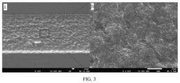
- FIG. 3 is a diagram of a surface shape of the single-crystal ⁇ -Ga 2 O 3 machined by the laser-assisted waterjet machining in Example 1, wherein, B is a partial enlargement of A.
- a method for preparing a single-crystal ⁇ -Ga 2 O 3 MSM detector comprising the steps of:
- the present process uses a nanosecond laser with a wavelength of 1064 nm, a laser pulse width of 30 ns and a pulse frequency of 315 kHz.
- the etching solution used for the present process is an HF solution with a solution concentration of 47-49% and an etching temperature of 5-25° C.
- a grinding fluid used in the present process is 1 ⁇ m of Al 2 O 3 grinding fluid, and a grinding disc is a softer grinding disc made of lead.
- a method for preparing a single-crystal ⁇ -Ga 2 O 3 MSM detector comprising the steps of:
- the present process uses a nanosecond laser with a wavelength of 1064 nm, a laser pulse width of 20 ns and a pulse frequency of 490 kHz.
- the etching solution used for the present process is an HF solution with a solution concentration of 47-49% and an etching temperature of 5-25° C.
- a grinding fluid used in the present process is 1 ⁇ m of Al 2 O 3 grinding fluid, and a grinding disc is a softer grinding disc made of lead.
- a method for preparing a single-crystal ⁇ -Ga 2 O 3 MSM detector comprising the steps of:
- the present process uses a nanosecond laser with a wavelength of 1064 nm, a laser pulse width of 10 ns and a pulse frequency of 1000 kHz.
- the etching solution used for the present process is an HF solution with a solution concentration of 47-49% and an etching temperature of 5-25° C.
- a grinding fluid used in the present process is 1 ⁇ m of Al 2 O 3 grinding fluid, and a grinding disc is a softer grinding disc made of lead.
Landscapes
- Chemical & Material Sciences (AREA)
- Organic Chemistry (AREA)
- Engineering & Computer Science (AREA)
- Materials Engineering (AREA)
- Metallurgy (AREA)
- Mechanical Engineering (AREA)
- Inorganic Chemistry (AREA)
- Chemical Kinetics & Catalysis (AREA)
- Crystallography & Structural Chemistry (AREA)
- Physics & Mathematics (AREA)
- Optics & Photonics (AREA)
- Plasma & Fusion (AREA)
- Crystals, And After-Treatments Of Crystals (AREA)
- Manufacturing & Machinery (AREA)
Abstract
A single-crystal β-Ga2O3 MSM detector and a preparation method thereof, comprising: machining grooves on a single-crystal β-Ga2O3 substrate using a laser-assisted waterjet machining technique to form a 3D shape; wet etching the machined single-crystal β-Ga2O3 substrate using an HF solution to remove machining damage; performing Au evaporation on a surface of the single-crystal β-Ga2O3 substrate after processing, coating an Au thin film on the surface of the single-crystal β-Ga2O3 substrate; and grinding the surface of the single-crystal β-Ga2O3 substrate after evaporation to remove the Au thin film on an undressed surface and retain the Au thin film in the grooves, and then obtaining the single-crystal β-Ga2O3 MSM detector.
Description
This application claims priority benefits to Chinese Patent Application No. 202211324539.3, filed 27 Oct. 2022, the contents of which are incorporated herein by reference.
The present invention belongs to the field of combined laser micro-machining technology, and specifically relates to a single-crystal β-Ga2O3 MSM (metal—semiconductor—metal) detector and a preparation method thereof.
The statements in this section merely provide background related to the present invention and do not necessarily constitute prior art.
Gallium oxide (β-Ga2O3), as a new generation of oxide semiconductor material, has advantages such as an ultra-wide forbidden band, high breakdown electric field strength, high UV transmittance, and stable physical and chemical properties. The Ga2O3 has an absorb edge of 240-280 nm, which is located in the solar blind ultraviolet (UV) band, and has good transmittance from the UV light to visible light, so it is an excellent solar blind detector material. However, because Ga2O3 is a hard and brittle material that is easy to dissociate, it is easy to produce scratches, dissociation pits, abrasive embedding, and other defects during precision machining. Meanwhile, due to the poor thermal conductivity and large anisotropy of single-crystal Ga2O3, it is easy to produce microcracks during laser machining. This greatly restricts the application and development of single-crystal Ga2O3.
The current preparation method of the β-Ga2O3 MSM detector is to carry out the photolithography on β-Ga2O3 thin film, and for the single-crystal β-Ga2O3 substrate, if it is machined by photolithography again, it cannot give full play to the advantages of the single-crystal β-Ga2O3 substrate (the photolithography on the MSM detector is to carry out the process in 2D directions on the substrate surface, which is suitable for application on β-Ga2O3 thin film substrates. For the single-crystal substrates, the surface of the substrate can be machined into a 3D shape by etching, laser and other machining methods, thus increasing Ohmic contact area between the metal and β-Ga2O3). Therefore, it is necessary to process the 3D shape on the single-crystal β-Ga2O3 substrate. At present, the machining method of single-crystal Ga2O3 is mainly wet etching, although it is not chemically resistant like sapphire (Al2O3), β-Ga2O3 is still difficult to wet etch, and in sputtered Ga2O3 thin films deposited at substrate temperature of 400-1000° C., an etching rate of Ga2O3 grown at 400° C. is about 490 nm/s, while the etching rate of the thin film grown at 1000° C. is only about 0.196 nm/s.
For existing technology that existed in the inadequacies, it is an object of the present invention to provide a single-crystal β-Ga2O3 MSM detector and a preparation method thereof.
To achieve the above purpose, the present invention is realized by the following technical solutions:
In a first aspect of the present invention, a method for preparing a single-crystal β-Ga2O3 MSM detector is provided, comprising the following steps:
machining grooves on a single-crystal β-Ga2O3 substrate using a laser-assisted waterjet machining technique to form a 3D shape;
wet etching the machined single-crystal β-Ga2O3 substrate using an HF (Hydrofluoric Acid) solution to remove machining damage;
performing Au evaporation on a surface of the single-crystal β-Ga2O3 substrate after processing, coating an Au thin film on the surface of the single-crystal β-Ga2O3 substrate; and
grinding a surface of the single-crystal β-Ga2O3 substrate after evaporation to remove the Au thin film on an undressed surface and retain the Au thin film in the grooves, then obtaining the single-crystal β-Ga2O3 MSM detector.
In some examples, the groove is an inverted trapezoidal groove.
In some examples, in the laser-assisted waterjet machining technique, the pulse width of a nanosecond laser is 10-350 ns, the pulse repetition frequency is 20-1000 kHz, the scanning speed is 1-16 mm/s, and the waterjet pressure is 4-16 MPa.
Preferably, the waterjet pressure is 5-10 MPa.
Preferably, the wavelength of the nanosecond laser is 1064 nm.
Further preferably, the laser single-pulse energy is 0.02-0.1 mJ and the focal plane focal is −0.1-0.1 mm.
Preferably, in the laser-assisted waterjet machining technique, the target distance of the nozzle of the waterjet is 0.3-1.4 mm, the offset distance of the waterjet is 0.3-0.7 mm, and the impact angle of the waterjet is 39°-51°.
The waterjet may gradually diverge with the increase of the target distance, and if the target distance is too large, the quality of the waterjet impinging on the surface of the workpiece is poor, and the water layer formed on the surface of the workpiece is unstable, which will make the laser unstable after passing through the water layer, thus affecting the machining quality; if the target distance is too small, the impact of the waterjet on the workpiece is large; meanwhile, due to the limitation of the shape of the nozzle, the minimum target distance is 0.3 mm.
The stress on the surface of the workpiece caused by the impact of the waterjet can be divided into a wall compressive stress and a wall shear stress. Wherein, the wall shear stress is the influencing factor of material removal. If the impact angle is too large, the wall shear stress is small and the material cannot be removed; if the impact angle is too small, the wall shear stress is large, and then the material will have a large area of brittle peeling in the machining, resulting in poor machining quality.
In some examples, the concentration of the HF solution for wet etching is 47-49%, the etching temperature is 5-25° C., and the etching time is 8-15 min.
The following is a reaction mechanism for wet etching of β-Ga2O3 in HF solution:
Ga 2 O 3+6HF→2GaF 3+3H 2 O
Ga 2 O 3+6HF→2GaF 3+3H 2 O
In some examples, the grinding fluid used for the grinding is 1-2.5 μm of Al2O3 grinding fluid, and the grinding disc is a softer grinding disc made of lead.
In a second aspect of the present invention, a 3D single-crystal β-Ga2O3 MSM detector is provided, which is prepared by the preparation method described above.
The beneficial effects achieved by one or more examples of the present invention described above are as follows:
The material removal mechanism of the laser-assisted waterjet machining technique is not the same as that of laser machining, which uses high temperature to vaporize the material, while in the laser-assisted waterjet machining, the laser only has the effect of heating and softening the material, and the material is removed by the impact of high-pressure waterjet after softening, which greatly reduces the recast layer and thermal cracking and has the advantage of small machining damage.
The crossed inverted trapezoidal grooves provide more contact area for the Au thin film, which can form the Ohmic contact with a larger area between the electrode and the single-crystal β-Ga2O3 substrate, thus improving the sensitivity of the MSM solar blind detector and reducing the size of the detector.
The present invention combines the laser-assisted waterjet machining technique with wet etching, which can efficiently carry out a rough machining of the 3D shape by the laser-assisted waterjet machining technique, and remove the machining damage and reduce surface roughness by wet etching.
The accompanying drawings constituting a part of the present invention are used to provide a further understanding of the present invention. The exemplary examples of the present invention and descriptions thereof are used to explain the present invention, and do not constitute an improper limitation of the present invention.
It should be pointed out that the following detailed descriptions are all illustrative and are intended to provide further descriptions of the present invention. Unless otherwise specified, all technical and scientific terms used in the present invention have the same meaning as those usually understood by a person of ordinary skill in the art to which the present invention belongs.
The present invention will now be further described with reference to the accompanying drawings and examples.
As shown in FIG. 2 , a method for preparing a single-crystal β-Ga2O3 MSM detector, comprising the steps of:
1) Machining to prepare an inverted trapezoidal crossed groove structure using a laser-assisted waterjet.
The present process uses a nanosecond laser with a wavelength of 1064 nm, a laser pulse width of 30 ns and a pulse frequency of 315 kHz.
(1) cleaning a single-crystal β-Ga2O3 substrate with ultrasonic cleaning, and mounting the cleaned substrate on a laser-assisted waterjet transparent workbench;
(2) focusing the device to a height of a focal plane of the laser of 0 mm; adjusting the relative position of the laser and the waterjet to an angle of the waterjet of 45°, an offset distance of the waterjet of 0.5 mm and a target distance of a nozzle of the waterjet of 0.6 mm;
(3) setting the laser parameters to a pulse width of 30 ns, a pulse frequency of 315 kHz, an average power of the laser of 20 W, a scanning speed of 1 mm/s, a machining times of once and a lateral offset distance of 10 μm;
(4) adjusting a waterjet pressure of 6 MPa; and
(5) running a machining program for MSM structure machining, and obtaining the inverted trapezoidal groove after the machining with a depth of 15-25 μm and a width of 50-60 μm; a diagram of a shape of the single-crystal β-Ga2O3 machined by the laser-assisted waterjet machining, as shown in FIG. 3 .
2) Wet etching on the machined single-crystal β-Ga2O3.
The etching solution used for the present process is an HF solution with a solution concentration of 47-49% and an etching temperature of 5-25° C.
(1) cleaning and placing the single-crystal β-Ga2O3 substrate in a beaker;
(2) preparing the HF solution with a solubility of 49%;
(3) pouring the prepared HF solution into the beaker until the substrate is submerged and reacting for 10 min at room temperature (20° C.); and
(4) taking out and cleaning the substrate.
3) Evaporation of the single-crystal β-Ga2O3.
(1) mounting the processed single-crystal β-Ga2O3 substrate on an evaporation workbench;
(2) evaporating a surface of the single-crystal β-Ga2O3 substrate with a layer of nanoscale Au thin film; and
(3) taking out the substrate.
4) Grinding of the single-crystal β-Ga2O3.
A grinding fluid used in the present process is 1 μm of Al2O3 grinding fluid, and a grinding disc is a softer grinding disc made of lead.
(1) mounting the single-crystal β-Ga2O3 substrate on a grinding workbench;
(2) mounting the grinding disc made of lead, and spraying the 1 μm of Al2O3 grinding liquid on the grinding disc made of lead;
(3) starting the grinding equipment for grinding;
(4) taking out the single-crystal β-Ga2O3 substrate after grinding for a period of time and observing under a microscope whether the Au thin film on the micro-machined surface is completely removed, and if it is not completely removed, continuing the grinding until it is completely removed; and
(5) cleaning the grinded single-crystal β-Ga2O3 substrate, and then obtaining the single-crystal β-Ga2O3 MSM detector.
A method for preparing a single-crystal β-Ga2O3 MSM detector, comprising the steps of:
1) Machining to prepare an inverted trapezoidal crossed groove structure using a laser-assisted waterjet.
The present process uses a nanosecond laser with a wavelength of 1064 nm, a laser pulse width of 20 ns and a pulse frequency of 490 kHz.
(1) cleaning a single-crystal β-Ga2O3 substrate with ultrasonic cleaning, and mounting the cleaned substrate on a laser-assisted waterjet transparent workbench;
(2) focusing the device to a height of a focal plane of the laser of −0.1 mm; adjusting the relative position of the laser and the waterjet to an angle of the waterjet of 45°, an offset distance of the waterjet of 0.5 mm and a target distance of a nozzle of the waterjet of 0.6 mm;
(3) setting the laser parameters to a pulse width of 20 ns, a pulse frequency of 490 kHz, an average power of the laser of 25 W, a scanning speed of 1 mm/s, a machining times of twice and a lateral offset distance of 15 μm;
(4) adjusting a waterjet pressure of 6 MPa; and
(5) running a machining program for MSM structure machining, and obtaining the inverted trapezoidal groove after the machining with a depth of 20-30 μm and a width of 60-70 μm.
2) Wet etching on the machined single-crystal β-Ga2O3.
The etching solution used for the present process is an HF solution with a solution concentration of 47-49% and an etching temperature of 5-25° C.
(1) cleaning and placing the single-crystal β-Ga2O3 substrate in a beaker;
(2) preparing the HF solution with a solubility of 47%;
(3) pouring the prepared HF solution into the beaker until the substrate is submerged and reacting for 10 min at room temperature (25° C.); and
(4) taking out and cleaning the substrate.
3) Evaporation of the single-crystal β-Ga2O3.
(1) mounting the processed single-crystal β-Ga2O3 substrate on an evaporation workbench;
(2) evaporating a surface of the single-crystal β-Ga2O3 substrate with a layer of nanoscale Au thin film; and
(3) taking out the substrate.
4) Grinding of the single-crystal β-Ga2O3.
A grinding fluid used in the present process is 1 μm of Al2O3 grinding fluid, and a grinding disc is a softer grinding disc made of lead.
(1) mounting the single-crystal β-Ga2O3 substrate on a grinding workbench;
(2) mounting the grinding disc made of lead, and spraying the 1 μm of Al2O3 grinding liquid on the grinding disc made of lead;
(3) starting the grinding equipment for grinding;
(4) taking out the single-crystal β-Ga2O3 substrate after grinding for a period and observing under a microscope whether the Au thin film on the micro-machined surface is completely removed, and if it is not completely removed, continuing the grinding until it is completely removed; and
(5) cleaning the grinded single-crystal β-Ga2O3 substrate, and then obtaining the single-crystal β-Ga2O3 MSM detector.
A method for preparing a single-crystal β-Ga2O3 MSM detector, comprising the steps of:
1) Machining to prepare an inverted trapezoidal crossed groove structure using a laser-assisted waterjet.
The present process uses a nanosecond laser with a wavelength of 1064 nm, a laser pulse width of 10 ns and a pulse frequency of 1000 kHz.
(1) cleaning a single-crystal β-Ga2O3 substrate with ultrasonic cleaning, and mounting the cleaned substrate on a laser-assisted waterjet transparent workbench;
(2) focusing the device to a height of a focal plane of the laser of 0.1 mm; adjusting the relative position of the laser and the waterjet to an angle of the waterjet of 45°, an offset distance of the waterjet of 0.5 mm and a target distance of a nozzle of the waterjet of 0.6 mm;
(3) setting the laser parameters to a pulse width of 10 ns, a pulse frequency of 1000 kHz, an average power of the laser of 30 W, a scanning speed of 1 mm/s, a machining times of 3 times and a lateral offset distance of 10 μm;
(4) adjusting a waterjet pressure of 6 MPa; and
(5) running a machining program for MSM structure machining, and obtaining the inverted trapezoidal groove after the machining with a depth of 10-15 μm and a width of 50-60 μm.
2) Wet etching on the machined single-crystal β-Ga2O3.
The etching solution used for the present process is an HF solution with a solution concentration of 47-49% and an etching temperature of 5-25° C.
(1) cleaning and placing the single-crystal β-Ga2O3 substrate in a beaker;
(2) preparing the HF solution with a solubility of 47%;
(3) pouring the prepared HF solution into the beaker until the substrate is submerged and reacting for 10 min at room temperature (15° C.); and
(4) taking out and cleaning the substrate.
3) Evaporation of the single-crystal β-Ga2O3.
(1) mounting the processed single-crystal β-Ga2O3 substrate on an evaporation workbench;
(2) evaporating a surface of the single-crystal β-Ga2O3 substrate with a layer of nanoscale Au thin film; and
(3) taking out the substrate.
4) Grinding of the single-crystal β-Ga2O3.
A grinding fluid used in the present process is 1 μm of Al2O3 grinding fluid, and a grinding disc is a softer grinding disc made of lead.
(1) mounting the single-crystal β-Ga2O3 substrate on a grinding workbench;
(2) mounting the grinding disc made of lead, and spraying the 1 μm of Al2O3 grinding liquid on the grinding disc made of lead;
(3) starting the grinding equipment for grinding;
(4) taking out the single-crystal β-Ga2O3 substrate after grinding for a period of time and observing under a microscope whether the Au thin film on the micro-machined surface is completely removed, and if it is not completely removed, continuing the grinding until it is completely removed; and
(5) cleaning the grinded single-crystal β-Ga2O3 substrate, and then obtaining the single-crystal β-Ga2O3 MSM detector.
The foregoing descriptions are merely preferred examples of the present invention but are not intended to limit the present invention. A person skilled in art may make various alterations and variations to the present invention. Any modification, equivalent replacement, or improvement made within the spirit and principles of the present invention shall fall within the protection scope of the present invention.
Claims (10)
1. A method for preparing a single-crystal β-Ga2O3 MSM detector is provided, comprising the following steps:
machining grooves on a single-crystal β-Ga2O3 substrate using a laser-assisted waterjet machining technique to form a 3D shape;
wet etching the machined single-crystal β-Ga2O3 substrate using an HF (Hydrofluoric Acid) solution to remove machining damage;
performing Au evaporation on a surface of the single-crystal β-Ga2O3 substrate after processing, coating an Au thin film on the surface of the single-crystal β-Ga2O3 substrate; and
grinding the surface of the single-crystal β-Ga2O3 substrate after evaporation to remove the Au thin film on an undressed surface and retain the Au thin film in the grooves, then obtaining the single-crystal β-Ga2O3 MSM detector.
2. The method for preparing the single-crystal β-Ga2O3 MSM detector according to claim 1 , wherein: the groove is an inverted trapezoidal groove.
3. The method for preparing the single-crystal β-Ga2O3 MSM detector according to claim 1 , wherein: in the laser-assisted waterjet machining technique, a pulse width of a nanosecond laser is 10-350 ns, a pulse repetition frequency is 20-1000 kHz, a scanning speed is 1-16 mm/s, and a waterjet pressure is 4-16 MPa.
4. The method for preparing the single-crystal β-Ga2O3 MSM detector according to claim 3 , wherein: a wavelength of the nanosecond laser is 1064 nm.
5. The method for preparing the single-crystal β-Ga2O3 MSM detector according to claim 3 , wherein: single-pulse energy of the nanosecond laser is 0.02-0.1 mJ, a height of a focal plane is −0.1-0.1 mm.
6. The method for preparing the single-crystal β-Ga2O3 MSM detector according to claim 1 , wherein: in the laser-assisted waterjet machining technique, a target distance of a nozzle of the waterjet is 0.3-1.4 mm, an offset distance of the waterjet is 0.3-0.7 mm, and an impact angle of the waterjet is 39°-51°.
7. The method for preparing the single-crystal β-Ga2O3 MSM detector according to claim 1 , wherein: a concentration of the HF solution for the wet etching is 47-49%.
8. The method for preparing the single-crystal β-Ga2O3 MSM detector according to claim 1 , wherein: an etching temperature is 5-25° C., and an etching time is 8-15 min.
9. The method for preparing the single-crystal β-Ga2O3 MSM detector according to claim 1 , wherein: a grinding fluid used for the grinding is a 1-2.5 μm of Al2O3 grinding fluid, a grinding disc is a softer grinding disc made of lead.
10. A 3D single-crystal β-Ga2O3 MSM detector, being prepared by the preparation method of any one of claim 1 .
Applications Claiming Priority (2)
| Application Number | Priority Date | Filing Date | Title |
|---|---|---|---|
| CN202211324539.3A CN115566104B (en) | 2022-10-27 | 2022-10-27 | Monocrystalline beta-Ga2O3MSM type detector and preparation method thereof |
| CN202211324539.3 | 2022-10-27 |
Publications (1)
| Publication Number | Publication Date |
|---|---|
| US11735683B1 true US11735683B1 (en) | 2023-08-22 |
Family
ID=84769103
Family Applications (1)
| Application Number | Title | Priority Date | Filing Date |
|---|---|---|---|
| US18/169,552 Active US11735683B1 (en) | 2022-10-27 | 2023-02-15 | Single-crystal beta-Ga2O3 MSM detector and preparation method thereof |
Country Status (2)
| Country | Link |
|---|---|
| US (1) | US11735683B1 (en) |
| CN (1) | CN115566104B (en) |
Cited By (1)
| Publication number | Priority date | Publication date | Assignee | Title |
|---|---|---|---|---|
| CN119779782A (en) * | 2024-12-18 | 2025-04-08 | 湖北九峰山实验室 | A method for characterizing dislocations in gallium oxide single crystals based on mechanical exfoliation |
Families Citing this family (1)
| Publication number | Priority date | Publication date | Assignee | Title |
|---|---|---|---|---|
| CN117855049B (en) * | 2024-02-01 | 2025-09-19 | 中国科学院半导体研究所 | Gallium oxide substrate and preparation method thereof |
Citations (1)
| Publication number | Priority date | Publication date | Assignee | Title |
|---|---|---|---|---|
| US20190019901A1 (en) * | 2017-07-14 | 2019-01-17 | The Board Of Trustees Of The University Of Illinois | Optoelectronic device having an antireflective surface |
Family Cites Families (8)
| Publication number | Priority date | Publication date | Assignee | Title |
|---|---|---|---|---|
| KR100787272B1 (en) * | 2003-02-24 | 2007-12-20 | 각코호진 와세다다이가쿠 | Ga2o3 light-emitting device, and its manufacturing method |
| CN104439710B (en) * | 2014-11-07 | 2017-02-15 | 江南大学 | Water jet assisted laser chemical etching device and method |
| CN113702447B (en) * | 2020-05-22 | 2022-10-14 | 中国科学院苏州纳米技术与纳米仿生研究所 | Gallium oxide nano-structure device and preparation method and application thereof |
| CN111710734B (en) * | 2020-06-19 | 2022-05-13 | 中国科学技术大学 | Gallium oxide photoelectric detector and preparation method thereof |
| CN111940907A (en) * | 2020-07-28 | 2020-11-17 | 南京理工大学 | Device and method for preparing micro-nano structure by flowing water assisted ultrafast laser |
| CN112038443B (en) * | 2020-08-31 | 2022-06-17 | 浙江大学 | Preparation method of gallium oxide polycrystalline thin film transistor type ultraviolet detector |
| CN114744059B (en) * | 2022-04-08 | 2023-03-24 | 中国科学院半导体研究所 | Solar blind polarization detector based on gallium oxide single crystal and preparation method thereof |
| CN115000203B (en) * | 2022-06-20 | 2023-11-21 | 山东大学 | Single crystal silicon micro-nano double-scale antireflection suede and preparation method thereof |
-
2022
- 2022-10-27 CN CN202211324539.3A patent/CN115566104B/en active Active
-
2023
- 2023-02-15 US US18/169,552 patent/US11735683B1/en active Active
Patent Citations (1)
| Publication number | Priority date | Publication date | Assignee | Title |
|---|---|---|---|---|
| US20190019901A1 (en) * | 2017-07-14 | 2019-01-17 | The Board Of Trustees Of The University Of Illinois | Optoelectronic device having an antireflective surface |
Cited By (1)
| Publication number | Priority date | Publication date | Assignee | Title |
|---|---|---|---|---|
| CN119779782A (en) * | 2024-12-18 | 2025-04-08 | 湖北九峰山实验室 | A method for characterizing dislocations in gallium oxide single crystals based on mechanical exfoliation |
Also Published As
| Publication number | Publication date |
|---|---|
| CN115566104B (en) | 2025-11-11 |
| CN115566104A (en) | 2023-01-03 |
Similar Documents
| Publication | Publication Date | Title |
|---|---|---|
| US11735683B1 (en) | Single-crystal beta-Ga2O3 MSM detector and preparation method thereof | |
| US11014197B2 (en) | Picosecond-nanosecond laser composite asynchronous ceramics polishing method | |
| US4539050A (en) | Process for the manufacture of semiconductor wafers with a rear side having a gettering action | |
| CN104498957B (en) | A kind of preparation method of the super-hydrophobic micro-nano structure of titanium alloy surface | |
| CN101621026B (en) | Back laser cutting method of glass passivated silicon wafer | |
| TW202030164A (en) | Microstructured glass substrate and method for manufacturing microstructured glass substrate | |
| CN112620947B (en) | Laser preparation method of vein bionic surface diamond cutting tool | |
| CN112620973B (en) | Unidirectional three-layer bidirectional six-stage step cutting process for silicon carbide wafer | |
| CN108166066A (en) | Laser crystal plasma modification etching auxiliary polishing processing method | |
| CN110526205A (en) | A method for plasma etching assisted laser processing of silicon carbide | |
| CN105932078A (en) | Texturing method of polycrystalline silicon wafer cut by diamond wire | |
| CN106541506B (en) | Laser crystal plasmaassisted lithography method | |
| CN104439710B (en) | Water jet assisted laser chemical etching device and method | |
| WO2015046412A1 (en) | Quartz glass component and method for producing quartz glass component | |
| CN118060752A (en) | Invisible wafer dicing method and its application | |
| CN103952670B (en) | Laser film quantification research method based on artificial defects | |
| CN117773661A (en) | A CVD diamond polishing method based on nanosecond laser and composite ion beam etching | |
| CN116921852B (en) | Ultrashort pulse laser processing methods and systems | |
| CN111549379B (en) | A kind of plasma modification and etching integrated crystal ultra-smooth surface processing method | |
| WO2019075789A1 (en) | Processing method for etching and cutting sapphire by means of laser-induced koh chemical reaction | |
| Li et al. | Analysis and comparison of laser cutting performance of solar float glass with different scanning modes | |
| CN112979170B (en) | Laser-assisted chemical corrosion processing method | |
| JP2013201223A (en) | Cover glass for solar cell | |
| CN119927443B (en) | A gallium nitride material etching method and etching system | |
| CN115255681A (en) | Method for stripping diamond crystal from inner layer by femtosecond laser |
Legal Events
| Date | Code | Title | Description |
|---|---|---|---|
| FEPP | Fee payment procedure |
Free format text: ENTITY STATUS SET TO UNDISCOUNTED (ORIGINAL EVENT CODE: BIG.); ENTITY STATUS OF PATENT OWNER: SMALL ENTITY |
|
| FEPP | Fee payment procedure |
Free format text: ENTITY STATUS SET TO SMALL (ORIGINAL EVENT CODE: SMAL); ENTITY STATUS OF PATENT OWNER: SMALL ENTITY |
|
| STCF | Information on status: patent grant |
Free format text: PATENTED CASE |