US11715976B2 - Coil component - Google Patents
Coil component Download PDFInfo
- Publication number
- US11715976B2 US11715976B2 US16/802,372 US202016802372A US11715976B2 US 11715976 B2 US11715976 B2 US 11715976B2 US 202016802372 A US202016802372 A US 202016802372A US 11715976 B2 US11715976 B2 US 11715976B2
- Authority
- US
- United States
- Prior art keywords
- coil
- lines
- turn
- virtual line
- coil pattern
- Prior art date
- Legal status (The legal status is an assumption and is not a legal conclusion. Google has not performed a legal analysis and makes no representation as to the accuracy of the status listed.)
- Active, expires
Links
- 239000000758 substrate Substances 0.000 claims description 56
- 239000004020 conductor Substances 0.000 claims description 43
- 230000002093 peripheral effect Effects 0.000 claims description 41
- 230000000149 penetrating effect Effects 0.000 claims description 11
- 230000005540 biological transmission Effects 0.000 description 49
- 230000009467 reduction Effects 0.000 description 15
- 230000007704 transition Effects 0.000 description 14
- 230000004048 modification Effects 0.000 description 12
- 238000012986 modification Methods 0.000 description 12
- 230000000694 effects Effects 0.000 description 7
- 230000008859 change Effects 0.000 description 3
- 238000010586 diagram Methods 0.000 description 3
- 238000004519 manufacturing process Methods 0.000 description 3
- 239000000463 material Substances 0.000 description 3
- 230000008901 benefit Effects 0.000 description 2
- 230000004907 flux Effects 0.000 description 2
- 230000020169 heat generation Effects 0.000 description 2
- 239000011347 resin Substances 0.000 description 2
- 229920005989 resin Polymers 0.000 description 2
- 239000004593 Epoxy Substances 0.000 description 1
- 239000002131 composite material Substances 0.000 description 1
- 238000001514 detection method Methods 0.000 description 1
- 239000004744 fabric Substances 0.000 description 1
- 239000011521 glass Substances 0.000 description 1
- 238000009499 grossing Methods 0.000 description 1
- 230000002452 interceptive effect Effects 0.000 description 1
- 238000003475 lamination Methods 0.000 description 1
- 239000000696 magnetic material Substances 0.000 description 1
- 230000007246 mechanism Effects 0.000 description 1
- 229910000889 permalloy Inorganic materials 0.000 description 1
- 230000035699 permeability Effects 0.000 description 1
- 229910000859 α-Fe Inorganic materials 0.000 description 1
Images


Classifications
-
- H—ELECTRICITY
- H01—ELECTRIC ELEMENTS
- H01F—MAGNETS; INDUCTANCES; TRANSFORMERS; SELECTION OF MATERIALS FOR THEIR MAGNETIC PROPERTIES
- H01F38/00—Adaptations of transformers or inductances for specific applications or functions
- H01F38/14—Inductive couplings
-
- H04B5/26—
-
- H—ELECTRICITY
- H02—GENERATION; CONVERSION OR DISTRIBUTION OF ELECTRIC POWER
- H02J—CIRCUIT ARRANGEMENTS OR SYSTEMS FOR SUPPLYING OR DISTRIBUTING ELECTRIC POWER; SYSTEMS FOR STORING ELECTRIC ENERGY
- H02J50/00—Circuit arrangements or systems for wireless supply or distribution of electric power
- H02J50/10—Circuit arrangements or systems for wireless supply or distribution of electric power using inductive coupling
-
- H—ELECTRICITY
- H01—ELECTRIC ELEMENTS
- H01F—MAGNETS; INDUCTANCES; TRANSFORMERS; SELECTION OF MATERIALS FOR THEIR MAGNETIC PROPERTIES
- H01F27/00—Details of transformers or inductances, in general
- H01F27/24—Magnetic cores
- H01F27/255—Magnetic cores made from particles
-
- H—ELECTRICITY
- H01—ELECTRIC ELEMENTS
- H01F—MAGNETS; INDUCTANCES; TRANSFORMERS; SELECTION OF MATERIALS FOR THEIR MAGNETIC PROPERTIES
- H01F27/00—Details of transformers or inductances, in general
- H01F27/28—Coils; Windings; Conductive connections
- H01F27/2804—Printed windings
-
- H—ELECTRICITY
- H01—ELECTRIC ELEMENTS
- H01F—MAGNETS; INDUCTANCES; TRANSFORMERS; SELECTION OF MATERIALS FOR THEIR MAGNETIC PROPERTIES
- H01F27/00—Details of transformers or inductances, in general
- H01F27/28—Coils; Windings; Conductive connections
- H01F27/2823—Wires
- H01F27/2828—Construction of conductive connections, of leads
-
- H—ELECTRICITY
- H01—ELECTRIC ELEMENTS
- H01F—MAGNETS; INDUCTANCES; TRANSFORMERS; SELECTION OF MATERIALS FOR THEIR MAGNETIC PROPERTIES
- H01F27/00—Details of transformers or inductances, in general
- H01F27/28—Coils; Windings; Conductive connections
- H01F27/2871—Pancake coils
-
- H—ELECTRICITY
- H01—ELECTRIC ELEMENTS
- H01F—MAGNETS; INDUCTANCES; TRANSFORMERS; SELECTION OF MATERIALS FOR THEIR MAGNETIC PROPERTIES
- H01F5/00—Coils
- H01F5/003—Printed circuit coils
-
- H—ELECTRICITY
- H01—ELECTRIC ELEMENTS
- H01F—MAGNETS; INDUCTANCES; TRANSFORMERS; SELECTION OF MATERIALS FOR THEIR MAGNETIC PROPERTIES
- H01F5/00—Coils
- H01F5/04—Arrangements of electric connections to coils, e.g. leads
-
- H—ELECTRICITY
- H02—GENERATION; CONVERSION OR DISTRIBUTION OF ELECTRIC POWER
- H02J—CIRCUIT ARRANGEMENTS OR SYSTEMS FOR SUPPLYING OR DISTRIBUTING ELECTRIC POWER; SYSTEMS FOR STORING ELECTRIC ENERGY
- H02J50/00—Circuit arrangements or systems for wireless supply or distribution of electric power
- H02J50/10—Circuit arrangements or systems for wireless supply or distribution of electric power using inductive coupling
- H02J50/12—Circuit arrangements or systems for wireless supply or distribution of electric power using inductive coupling of the resonant type
-
- H—ELECTRICITY
- H02—GENERATION; CONVERSION OR DISTRIBUTION OF ELECTRIC POWER
- H02J—CIRCUIT ARRANGEMENTS OR SYSTEMS FOR SUPPLYING OR DISTRIBUTING ELECTRIC POWER; SYSTEMS FOR STORING ELECTRIC ENERGY
- H02J50/00—Circuit arrangements or systems for wireless supply or distribution of electric power
- H02J50/40—Circuit arrangements or systems for wireless supply or distribution of electric power using two or more transmitting or receiving devices
- H02J50/402—Circuit arrangements or systems for wireless supply or distribution of electric power using two or more transmitting or receiving devices the two or more transmitting or the two or more receiving devices being integrated in the same unit, e.g. power mats with several coils or antennas with several sub-antennas
-
- H—ELECTRICITY
- H04—ELECTRIC COMMUNICATION TECHNIQUE
- H04B—TRANSMISSION
- H04B5/00—Near-field transmission systems, e.g. inductive loop type
- H04B5/0025—Near field system adaptations
- H04B5/0037—Near field system adaptations for power transfer
-
- H—ELECTRICITY
- H04—ELECTRIC COMMUNICATION TECHNIQUE
- H04B—TRANSMISSION
- H04B5/00—Near-field transmission systems, e.g. inductive loop type
- H04B5/0075—Near-field transmission systems, e.g. inductive loop type using inductive coupling
- H04B5/0081—Near-field transmission systems, e.g. inductive loop type using inductive coupling with antenna coils
-
- H04B5/79—
-
- H—ELECTRICITY
- H01—ELECTRIC ELEMENTS
- H01F—MAGNETS; INDUCTANCES; TRANSFORMERS; SELECTION OF MATERIALS FOR THEIR MAGNETIC PROPERTIES
- H01F27/00—Details of transformers or inductances, in general
- H01F27/28—Coils; Windings; Conductive connections
- H01F27/2804—Printed windings
- H01F2027/2809—Printed windings on stacked layers
Definitions
- the present invention relates to a coil component and, more particularly, to a coil component suitable for use in wireless power transmission systems.
- wireless power transmission systems that feed electric power from a power transmitting side to a power receiving side by wireless are put in practical use.
- the wireless power transmission systems are expected to be applied to various products including transport equipment such as electric trains or electric cars, household appliances, electronic equipment, wireless communication devices, toys, and industrial equipment.
- transport equipment such as electric trains or electric cars, household appliances, electronic equipment, wireless communication devices, toys, and industrial equipment.
- JP 2018-102124A and Japanese Patent No. 5,686,769 propose a wireless power transmission system provided with a plurality of power transmitting coils on the power transmitting side.
- JP 1996-203739A and JP 2003-197438A disclose a coil component having a configuration in which a planar spiral conductor formed on the surface of an insulating substrate is radially divided by a spiral slit.
- a planar conductor is thus radially divided by the spiral slit, uneven distribution of current density is reduced, allowing a reduction in DC resistance or AC resistance.
- a coil component according to the present invention has a first coil pattern wound in a planar spiral shape, wherein at least one turn constituting the first coil pattern is divided into a plurality of lines by a spiral slit, and a space width between the plurality of lines differs depending on a planar position.
- the present invention since at least one turn of the first coil pattern is divided into a plurality of lines, uneven distribution of current density is reduced, with the result that DC resistance or AC resistance can be reduced.
- the space width between the plurality of lines differs depending on the planar position, the outer shape of the first coil pattern, the shape and position of an inner diameter area thereof can be easily finely adjusted by the design of the space width.
- a space width along the first virtual line and a space width along the second virtual line may differ from each other.
- a space width along the first and third virtual lines may be larger than a space width along the second and fourth virtual lines, or a space width along the first virtual line may be larger than a space width along the second and third virtual lines.
- a coil component having an outer shape whose horizontal size is larger than the vertical size in the latter case, there can be provided a coil component in which the position of the inner diameter position is off-centered.
- the coil component according to the present invention may further have a second coil pattern wound in a planar spiral shape, wherein at least one turn constituting the second coil pattern may be divided into a plurality of lines by a spiral slit, and when a fourth virtual line extending in the first direction with a second reference point positioned in an inner diameter area of the second coil pattern as a starting point and a fifth virtual line extending in a direction 180° opposite to the first direction with the second reference point as a starting point are defined, a space width between the plurality of lines may be larger along the fifth virtual line than along the fourth virtual line, and the first and second coil patterns may be disposed such that the third and fourth virtual lines overlap each other.
- a coil component including two coil patterns in each of which the position of the inner diameter area is off-centered.
- the coil component according to the present invention may further include a second coil pattern wound in a planar spiral shape, the first coil pattern may be formed on one surface of a first insulating substrate, the second coil pattern may be formed on the other surface of the first insulating substrate, the innermost turn of the first coil pattern may be divided by a spiral slit into a plurality of lines including first and second lines, the innermost turn of the second coil pattern may be divided by a spiral slit into a plurality of lines including third and fourth lines, the first line may be positioned on the inner peripheral side with respect to the second line, the third line may be positioned on the inner peripheral side with respect to the fourth line, the inner peripheral ends of the first and fourth lines may be connected to each other through a first through hole conductor penetrating the first insulating substrate, and the inner peripheral ends of the second and third lines may be connected to each other through a second through hole conductor penetrating the first insulating substrate.
- the radial position of each line alternates between the first and second coil
- the coil component according to the present invention may further have a third coil pattern wound in a planar spiral shape, at least one turn constituting the third coil pattern may be divided into a plurality of lines by a spiral slit, and when a fifth virtual line extending in the first direction with the second reference point positioned in an inner diameter area of the third coil pattern as a starting point and a sixth virtual line extending in the third direction with the second reference point as a starting point are defined, a space width between the plurality of lines may be larger along the fifth virtual line than along the sixth virtual line, and the first and third coil patterns may overlap each other such that the sixth virtual line passes the inner diameter area of the first coil pattern in a plan view.
- the coil component according to the present invention is used as a power transmitting coil of a wireless power transmission system, it is possible to suppress a reduction in transmission efficiency even when a power receiving coil is positioned between the first and third coil patterns in a plan view.
- the coil component according to the present invention may further has a switch that exclusively supply current to one of the first and third coil patterns.
- a switch that exclusively supply current to one of the first and third coil patterns.
- the coil component according to the present invention may further include a fourth coil pattern wound in a planar spiral shape, the third coil pattern may be formed on one surface of a second insulating substrate, the fourth coil pattern may be formed on the other surface of the second insulating substrate, the innermost turn of the third coil pattern may be divided by a spiral slit into a plurality of lines including fifth and sixth lines, the innermost turn of the fourth coil pattern may be divided by a spiral slit into a plurality of lines including seventh and eighth lines, the fifth line may be positioned on the inner peripheral side with respect to the sixth line, the seventh line may be positioned on the inner peripheral side with respect to the eighth line, the inner peripheral ends of the fifth and eighth lines may be connected to each other through a third through hole conductor penetrating the second insulating substrate, and the inner peripheral ends of the sixth and seventh lines may be connected to each other through a fourth through hole conductor penetrating the second insulating substrate.
- the radial position of each line alternates between the third and fourth coil
- the coil component according to the present invention may further have a fifth coil pattern wound in a planar spiral shape, at least one turn constituting the fifth coil pattern may be divided into a plurality of lines by a spiral slit, and when a seventh virtual line extending in the first direction with a third reference point positioned in an inner diameter area of the fifth coil pattern as a starting point and an eighth virtual line extending in the third direction with the third reference point as a starting point are defined, a space width between the plurality of lines may be larger along the eighth virtual line than along the seventh virtual line, and the first and fifth coil patterns may overlap each other such that the seventh virtual line passes the inner diameter area of the first coil pattern in a plan view.
- the coil component according to the present invention when used as a power transmitting coil of a wireless power transmission system, it is possible to suppress a reduction in transmission efficiency even when a power receiving coil is positioned between the first and third coil patterns or between the first and fifth coil patterns in a plan view.
- the third and fifth coil patterns may be formed on the same insulating substrate. This allows the relative position between the third and fifth coil patterns to be fixed.
- the first coil pattern may have an innermost turn positioned on the innermost peripheral side, an outermost turn positioned on the outermost peripheral side, and an intermediate turn whose turn number counting from the innermost or outermost turn is at the center of the total number of turns, the innermost turn, outermost turn, and intermediate turn may each be divided by a spiral slit into a plurality of lines, and the line width of each of the plurality of lines constituting each of the inner and outermost turns may be smaller than the line width of each of the plurality of lines constituting the intermediate turn. Since the line width of the innermost turn and that of the outermost turn are small, a loss caused due to the influence of a magnetic field can be reduced.
- the line width of each of the plurality of lines constituting the innermost turn may be smaller than the line width of each of the plurality of lines constituting the outermost turn, and this makes it possible to reduce the loss at the innermost turn to be exposed to a strongest magnetic field.
- the coil component according to the present invention may further have a sixth coil pattern wound in a planar spiral shape and a magnetic sheet, the first and sixth coil patterns may be disposed so as to overlap the magnetic sheet in a plan view, the first and sixth coil patterns may be connected in parallel, the first coil pattern is disposed closer to the magnetic sheet than the sixth coil pattern, a line length of the sixth coil pattern may be larger than that of the first coil pattern. Since a difference is provided between the line lengths of the first and sixth coil patterns, impedance of each coil pattern can be finely adjusted. This allows a difference in impedance between the first and sixth coil patterns can be reduced, so that the impedance difference in the entire coil component can be reduced. As a result, a loss caused due to the impedance difference can be reduced.
- a coil component having a high degree of freedom of design As described above, according to the present invention, there can be provided a coil component having a high degree of freedom of design.
- the coil component of the present invention when applied to a power transmitting coil of a wireless power transmission system, high transmission efficiency corresponding to the specification or shape of an application product can be ensured.
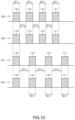
- FIG. 1 is a schematic cross-sectional view for explaining the configuration of a coil component according to a preferred embodiment of the present invention
- FIG. 2 is a plan view transparently illustrating the coil component shown in FIG. 1 ;
- FIGS. 3 A to 3 C are schematic plan views for explaining the planar shapes of the center coil, first side coil, and second side coil, respectively.
- FIG. 4 is a circuit diagram of the coil component shown in FIG. 1 ;
- FIG. 5 is a schematic view illustrating the outer appearance of a wireless power transmitting device when the coil component shown in FIG. 1 is used as a transmitting coil of a wireless power transmission system;
- FIG. 6 is a schematic view illustrating the configuration of the wireless power transmission system using the coil component shown in FIG. 1 ;
- FIG. 7 is a schematic plan view for explaining the pattern shape of the coil pattern 100 as viewed from the one sides of the insulating substrates;
- FIG. 8 is a schematic plan view for explaining the pattern shape of the coil pattern 200 as viewed from the other sides of the insulating substrates;
- FIG. 9 is an equivalent circuit diagram of the center coil
- FIGS. 10 to 14 are schematic cross-sectional views for explaining the line and space widths of each of the turns 110 , 120 , 130 , 140 , and 150 constituting the coil pattern shown in FIG. 7 ;
- FIG. 15 is a schematic plan view for explaining the pattern shapes of the respective coil patterns 300 and 500 as viewed from the one sides of the insulating substrates;
- FIG. 16 is a schematic plan view for explaining the pattern shapes of the respective coil patterns 400 and 600 as viewed from the other sides of the insulating substrates;
- FIGS. 17 to 21 are schematic cross-sectional views for explaining the line and space widths of each of the turns 310 , 320 , 330 , 340 , and 350 constituting the coil pattern shown in FIG. 15 ;
- FIG. 22 is a schematic plan view illustrating a state where the coil patterns 100 , 200 , 300 , 400 , 500 , and 600 overlap one another;
- FIG. 23 is a plan view transparently illustrating a coil component according to a first modification
- FIG. 24 is a schematic cross-sectional view for explaining the configuration of a coil component according to a second modification.
- FIG. 25 is a schematic cross-sectional view for explaining the configuration of a coil component according to a third modification.
- FIG. 1 is a schematic cross-sectional view for explaining the configuration of a coil component 1 according to a preferred embodiment of the present invention.
- the coil component 1 includes a magnetic sheet 2 , a center coil C 0 , a first side coil C 1 , and a second side coil C 2 each of which is disposed so as to overlap the magnetic sheet 2 .
- the magnetic sheet 2 is a sheet member made of as high permeability material such as ferrite, permalloy, or a composite magnetic material and functions as a magnetic path for magnetic flux that interlinks with the center coil C 0 and side coils C 1 , C 2 .
- the coil component 1 according to the present embodiment can be used as a power transmitting coil of a wireless power transmission system.
- a power receiving coil is disposed on a power receiving surface 3 positioned on the side opposite to the magnetic sheet 2 with respect to the center coil C 0 and side coils C 1 , C 2 .
- the center coil C 0 has coil patterns 100 A, 100 B, and 100 C formed respectively on one surfaces 11 , 21 , and 31 of substrates 10 , 20 , and 30 and coil patterns 200 A, 200 B, and 200 C formed respectively on the other surfaces 12 , 22 , and 32 of substrates 10 , 20 , and 30 .
- the first side coil C 1 has coil patterns 300 A, 300 B, and 300 C formed respectively on one surfaces 41 , 51 , and 61 of substrates 40 , 50 , and 60 , and coil patterns 400 A, 400 B, and 400 C formed respectively on the other surfaces 42 , 52 , and 62 of substrates 40 , 50 , and 60 .
- the second side coil C 2 has coil patterns 500 A, 500 B, and 500 C formed respectively on one surfaces 41 , 51 , and 61 of substrates 40 , 50 , and 60 , and coil patterns 600 A, 600 B, and 600 C formed respectively on the other surfaces 42 , 52 , and 62 of substrates 40 , 50 , and 60 .
- a film-shaped transparent or semi-transparent flexible material such as PET resin, having a thickness of about 10 ⁇ m to 50 ⁇ m can be used.
- the substrates 10 , 20 , 30 , 40 , 50 , and 60 may each be a flexible substrate obtained by impregnating glass cloth with epoxy-based resin.
- the coil patterns ( 100 A, 100 B, 100 C, 200 A, 200 B, and 200 C) constituting the center coil C 0 are the same in the number of turns
- the coil patterns ( 300 A, 300 B, 300 C, 400 A, 400 B, and 400 C) constituting the first side coil C 1 are the same in the number of turns
- the coil patterns ( 500 A, 500 B, 500 C, 600 A, 600 B, and 600 C) constituting the second side coil C 2 are the same in the number of turns.
- the coil patterns constituting the first side coil C 1 and the coil patterns constituting the second side coil C 2 are also the same in the number of turns.
- the coil patterns constituting the center coil C 0 and the coil patterns constituting the first side coil C 1 or second side coil C 2 may be the same or different in the number of turns.
- coil pattern 100 when there is no particular need to make a distinction between the coil patterns 100 A, 100 B, and 100 C, or when the coil patterns 100 A, 100 B, and 100 C are collectively referred to, they are sometimes simply referred to as “coil pattern 100 ”. The same applies to the other coil patterns 200 , 300 , 400 , 500 , and 600 .
- FIG. 2 is a plan view transparently illustrating the coil component 1 according to the present embodiment.
- the hatched areas are each a coil area including the entire coil pattern from its innermost turn to outermost turn, i.e., an area including the entire coil pattern excluding the inner diameter area of the coil pattern.
- the specific pattern shape within the coil area will be described later.
- a part of the coil area of the center coil C 0 has an overlap with the coil area of the first side coil C 1 in a plan view
- another part of the coil area of the center coil C 0 has an overlap with the coil area of the second side coil C 2 in a plan view.
- the coil area of the first side coil C 1 and the coil area of the second side coil C 2 do not have an overlap.
- the coil area of the first side coil C 1 and the coil area of the second side coil C 2 have shapes symmetric with respect to the center line of the center coil C 0 in the x-direction and are disposed symmetrically with respect thereto.
- the coil areas of the respective center coil C 0 , first side coil C 1 , and second side coil C 2 have the same width in the y-direction.
- the center coil C 0 , first side coil C 1 , and second side coil C 2 have their respective inner diameter areas 70 to 72 .
- the inner diameter area refers to an area surrounded by the coil pattern, where there is no conductor pattern. As illustrated in FIG. 2 , in the present embodiment, a part of the inner diameter area 70 of the center coil C 0 overlaps the coil area of the first side coil C 1 , and another part of the inner diameter area 70 of the center coil C 0 overlaps the coil area of the second side coil C 2 . Further, the inner diameter area 71 of the first side coil C 1 completely overlaps the coil area of the center coil C 0 , and the inner diameter area 72 of the second side coil C 2 completely overlaps the coil area of the center coil C 0 .
- the three coils C 0 to C 2 constituting the coil component 1 according to the present embodiment are disposed such that the x-direction positions thereof differ from one another, so that when the coil component 1 is used as a power transmitting coil of a wireless power transmission system, a power feedable area is enlarged in the x-direction.
- the center coil C 0 is used to perform power feeding when a power receiving coil exists in the area X 0 of FIG. 2 ;
- the first side coil C 1 is used to perform power feeding when a power receiving coil exists in the area X 1 ;
- the second side coil C 2 is used to perform power feeding when a power receiving coil exists in the area X 2 .
- the boundary between the areas X 0 and X 1 may be set between the inner diameter areas 70 and 71
- the boundary between the areas X 0 and X 2 may be set between the inner diameter areas 70 and 72 .
- FIGS. 3 A to 3 C are schematic plan views for explaining the planar shapes of the center coil C 0 , first side coil C 1 , and second side coil C 2 , respectively.
- the center coil C 0 is substantially rectangular in outer shape in which a size CW 0 x in the x-direction is larger than a size CW 0 y in the y-direction. That is,
- the inner shape of the center coil C 0 may be a square.
- an area positioned in the positive x-direction with respect to the inner diameter area 70 i.e., an area positioned at the 3 o'clock position with respect to the inner diameter area 70 has an x-direction width CW 0 x R and that an area positioned in the negative x-direction with respect to the inner diameter area 70 , i.e., an area positioned at the 9 o'clock position with respect to the inner diameter area 70 has an x-direction width CW 0 x L ,
- an area positioned in the positive y-direction with respect to the inner diameter area 70 i.e., an area positioned at the 12 o'clock position with respect to the inner diameter area 70 has a y-direction width CW 0 y T and that an area positioned in the negative y-direction with respect to the inner diameter area 70 , i.e., an area positioned at the 6 o'clock position with respect to the inner diameter area 70 has a y-direction width CW 0 y B ,
- the first side coil C 1 is substantially rectangular in outer shape in which a size CW 1 x in the x-direction is larger than a size CW 1 y in the y-direction. That is,
- the inner shape of the first side coil C 1 may be a square.
- an area positioned in the positive x-direction with respect to the inner diameter area 71 i.e., an area positioned at the 3 o'clock position with respect to the inner diameter area 71 has an x-direction width CW 1 x R and that an area positioned in the negative x-direction with respect to the inner diameter area 71 , i.e., an area positioned at the 9 o'clock position with respect to the inner diameter area 71 has an x-direction width CW 1 x L ,
- CW 1 x R >CW 1 x L is satisfied. That is, the inner diameter area 71 is decentered in the negative x-direction (leftward).
- an area positioned in the positive y-direction with respect to the inner diameter area 71 i.e., an area positioned at the 12 o'clock position with respect to the inner diameter area 71 has a y-direction width CW 1 y T and that an area positioned in the negative y-direction with respect to the inner diameter area 71 , i.e., an area positioned at the 6 o'clock position with respect to the inner diameter area 71 has a y-direction width CW 1 y B ,
- the second side coil C 2 is substantially rectangular in outer shape in which a size CW 2 x in the x-direction is larger than a size CW 2 y in the y-direction. That is,
- the inner shape of the second side coil C 2 may be a square.
- an area positioned in the positive x-direction with respect to the inner diameter area 72 i.e., an area positioned at the 3 o'clock position with respect to the inner diameter area 72 has an x-direction width CW 2 x R and that an area positioned in the negative x-direction with respect to the inner diameter area 72 , i.e., an area positioned at the 9 o'clock position with respect to the inner diameter area 72 has an x-direction width CW 2 x L ,
- CW 2 x R >CW 2 x L is satisfied. That is, the inner diameter area 72 is decentered in the positive x-direction (rightward).
- an area positioned in the positive y-direction with respect to the inner diameter area 72 i.e., an area positioned at the 12 o'clock position with respect to the inner diameter area 72 has a y-direction width CW 2 y T and that an area positioned in the negative y-direction with respect to the inner diameter area 72 , i.e., an area positioned at the 6 o'clock position with respect to the inner diameter area 72 has a y-direction width CW 2 y R ,
- the y-direction size D 0 y of the inner diameter area 70 may be equal to the y-direction sizes D 1 y and D 2 y of the respective inner diameter areas 71 and 72 . That is,
- the x-direction size D 0 x of the inner diameter area 70 may be larger than the x-direction sizes D 1 x and D 2 x of the respective inner diameter areas 71 and 72 . That
- the center coil C 0 has a substantially rectangular outer shape elongated in the x-direction, the inner diameter area 71 of the first side coil C 1 positioned in the positive x-direction (rightward) with respect to the center coil C 0 is decentered in the negative x-direction (leftward), and the inner diameter area 72 of the second side coil C 2 positioned in the negative x-direction (leftward) with respect to the center coil C 0 is decentered in the positive x-direction (rightward).
- the coil component 1 according to the present embodiment when used as a power transmitting coil of a wireless power transmission system, the following advantage can be obtained: even when the planar position of a power receiving coil deviates from the center coil C 0 to lower the efficiency of transmission using the center coil C 0 , efficient power transmission can be ensured by the first side coil C 1 or second side coil C 2 .
- FIG. 4 is a circuit diagram of the coil component 1 according to the present embodiment.
- the center coil C 0 has a configuration in which serially connected coil patterns 100 A, 200 A, serially connected coil patterns 100 B, 200 B, and serially connected coil patterns 100 C, 200 C are connected in parallel.
- the first side coil C 1 has a configuration in which serially connected coil patterns 300 A, 400 A, serially connected coil patterns 300 B, 400 B, and serially connected coil patterns 300 C, 400 C are connected in parallel.
- the second side coil C 2 has a configuration in which serially connected coil patterns 500 A, 600 A, serially connected coil patterns 500 B, 600 B, and serially connected coil patterns 500 C, 600 C are connected in parallel.
- the coil component 1 When the coil component 1 according to the present embodiment is used as a power transmitting coil of a wireless power transmission system, one of the center coil C 0 , side coil C 1 , and side coil C 2 is connected to a power transmitting circuit 4 through a switch 5 .
- the switch 5 is a circuit exclusively connecting the power transmitting circuit 4 and one of the coils C 0 , C 1 , and C 2 , and the switching of connection is controlled by a switching circuit 6 .
- current output from the power transmitting circuit 4 is supplied to one of the coils C 0 , C 1 , and C 2 .
- FIG. 5 is a schematic view illustrating the outer appearance of a wireless power transmitting device when the coil component 1 according to the present embodiment is used as a transmitting coil of a wireless power transmission system.
- the power receiving surface 3 constitutes the xy plane, and a wireless power receiving device RX is placed on the power receiving surface 3 .
- the wireless power receiving device RX is, for example, a mobile terminal such as a smartphone.
- the power receiving surface 3 and wireless power receiving device RX are not provided with a positioning mechanism for correctly positioning them, and the wireless power receiving device RX is placed on the power receiving surface 3 by a user without any particular care. Then, as illustrated in FIG. 5 , when the wireless power receiving device RX placed on the power receiving surface 3 exists in the area X 0 , the switching circuit 6 illustrated in FIG. 4 selects the center coil C 0 .
- the switching circuit 6 selects the first side coil C 1 . Further, when the wireless power receiving device RX placed on the power receiving surface 3 exists in the area X 2 , the switching circuit 6 selects the second side coil C 2 . As a result, proper power transmission can be performed regardless of the position of the wireless power receiving device RX on the power receiving surface 3 .
- the position of the wireless power receiving device RX may be determined directly by using a position sensor or the like or indirectly through detection of a change in impedance or in power waveform in the coil component 1 .
- FIG. 6 is a schematic view illustrating the configuration of the wireless power transmission system using the coil component 1 according to the present embodiment.
- the wireless power transmission system illustrated in FIG. 6 is a system including a wireless power transmitting device TX and a wireless power receiving device RX, and power transmitting coils C 0 to C 2 included in the wireless power transmitting device TX and a power receiving coil 7 included in the wireless power receiving device RX are made to face each other through a space 9 , whereby power transmission is performed by wireless.
- the power transmitting coils C 0 to C 2 are connected to the power transmitting circuit 4 including a power supply circuit, an inverter circuit, a resonant circuit, and the like to be supplied with AC current from the power transmitting circuit 4 .
- the power receiving coil 7 is connected to a power receiving circuit 8 including a resonant circuit, a rectifying circuit, a smoothing circuit, and the like.
- a power receiving circuit 8 including a resonant circuit, a rectifying circuit, a smoothing circuit, and the like.
- the magnetic sheets 2 are disposed, respectively, on the side opposite to the space 9 with respect to the power transmitting coils C 0 to C 2 and on the side opposite to the space 9 with respect to the power receiving coil 7 .
- the magnetic sheet 2 plays a role of increasing the inductances of the power transmitting coils C 0 to C 2 and power receiving coil 7 , thereby allowing achievement of more efficient power transmission.
- FIG. 7 is a schematic plan view for explaining the pattern shape of the coil pattern 100 as viewed from the one sides 11 , 21 , and 31 of the insulating substrates 10 , 20 , and 30 , respectively.
- the coil pattern 100 is constituted by a planar conductor spirally wound in a plurality of turns.
- the coil pattern 100 has a five-turn configuration including turns 110 , 120 , 130 , 140 , and 150 .
- the turn 110 constitutes the outermost turn
- the turn 150 constitutes the innermost turn.
- the turns 110 , 120 , 130 , 140 , and 150 are each radially divided into four parts by three spiral slits.
- the turn 110 is divided into lines 111 to 114 , the turn 120 is divided into lines 121 to 124 , the turn 130 is divided into lines 131 to 134 , the turn 140 is divided into lines 141 to 144 , and the turn 150 is divided into lines 151 to 154 .
- the line 111 constitutes the outermost line
- the line 154 constitutes the innermost line.
- the lines 111 to 114 of the outermost turn 110 are connected to a terminal electrode pattern 161 through a radially extending lead-out pattern 162 .
- a radially extending lead-out pattern 172 is disposed peripherally adjacent to the lead-out pattern 162 and is connected, at its leading end, to a terminal electrode pattern 171 .
- the inner peripheral ends of the respective lines 151 to 154 of the innermost turn 150 are connected, respectively, to through hole conductors T 11 to T 14 penetrating the insulating substrate ( 10 , 20 , 30 ).
- the turns 110 , 120 , 130 , 140 , and 150 constituting the coil pattern 100 each have linear areas 182 and 184 extending in the x-direction, linear areas 181 and 183 extending in the y-direction, and curved areas 191 to 194 positioned between the two adjacent linear areas.
- the linear area 182 includes a transition area 182 a as a boundary between the turns 110 , 120 , 130 , 140 , and 150 , and the turns 110 , 120 , 130 , 140 , and 150 each therefore obliquely extend by one turn in the y-direction.
- the width of lines in the same turn is constant, and the width of the same line changes between different turns. Further, in the same turn, a space width between lines differs depending on the planar position.
- the definitions of the “line width” and “space width” are as follows.
- a reference point CP 1 is set in the inner diameter area 70 .
- a virtual line L 11 extending in the positive x-direction is defined with the reference point CP 1 as a starting point
- a virtual line L 12 extending in the positive y-direction is defined with the reference point CP 1 as a starting point
- a virtual line L 13 extending in the negative x-direction is defined with the reference point CP 1 as a starting point
- a virtual line L 14 extending in the negative y-direction is defined with the reference point CP 1 as a starting point.
- the positive x-direction, positive y-direction, negative x-direction, and negative y-direction may be rephrased, respectively, as first to fourth directions D 1 to D 4 starting from the reference point CP 1 .
- the virtual lines L 11 to L 14 are perpendicular, respectively, to the linear areas 181 to 184 .
- the width of each of the lines along the virtual lines L 11 to L 14 is the “line width”
- the width of each of the spaces along the virtual lines L 11 to L 14 is the “space width”.
- the virtual line L 12 passes between the through hole conductors T 12 and T 13 , then passes the transition area 182 a , and passes between the lead-out patterns 162 and 172 .
- the positions of the through hole conductors T 11 and T 14 are symmetric with respect to the virtual line L 12
- the positions of the through hole conductors T 12 and T 13 are also symmetric with respect to the virtual line L 12 .
- the reference point CP 1 need not necessarily be set at the center point of the coil pattern 100 but may be offset in the x-direction so as not to make the virtual line L 12 pass the transition area 182 a.
- FIG. 8 is a schematic plan view for explaining the pattern shape of the coil pattern 200 as viewed from the other sides 12 , 22 , and 32 of the insulating substrates 10 , 20 , and 30 , respectively.
- the coil pattern 200 has the same pattern shape as the coil pattern 100 .
- the coil patterns 100 and 200 can be produced using the same mask, allowing a significant reduction in manufacturing cost.
- the coil pattern 200 has a five-turn configuration including turns 210 , 220 , 230 , 240 , and 250 .
- the turn 210 constitutes the outermost turn, and the turn 250 constitutes the innermost turn.
- the turns 210 , 220 , 230 , 240 , and 250 are each radially divided into four parts by three spiral slits.
- the turn 210 is divided into lines 211 to 214
- the turn 220 is divided into lines 221 to 224
- the turn 230 is divided into lines 231 to 234
- the turn 240 is divided into lines 241 to 244
- the turn 250 is divided into lines 251 to 254 .
- the line 211 constitutes the outermost line
- the line 254 constitutes the innermost line.
- the lines 211 to 214 of the outermost turn 210 are connected to a terminal electrode pattern 261 through a radially extending lead-out pattern 262 .
- a radially extending lead-out pattern 272 is disposed peripherally adjacent to the lead-out pattern 262 and is connected, at its leading end, to a terminal electrode pattern 271 .
- the lead-out pattern 272 is connected to the lead-out pattern 162 illustrated in FIG. 7 through a plurality of through hole conductors T 15 .
- the lead-out pattern 262 is connected to the lead-out pattern 172 illustrated in FIG. 7 through a plurality of through hole conductors T 16 .
- the inner peripheral ends of the respective lines 251 to 254 of the innermost turn 250 are connected, respectively, to through hole conductors T 14 to T 11 .
- the inner peripheral ends of the respective lines 251 to 254 are connected, respectively, to the inner peripheral ends of the lines 154 , 153 , 152 , and 151 of the coil pattern 100 .
- the turns 210 , 220 , 230 , 240 , and 250 constituting the coil pattern 200 each have linear areas 282 and 284 extending in the x-direction, linear areas 281 and 283 extending in the y-direction, and curved areas 291 to 294 positioned between the two adjacent linear areas.
- the linear area 282 includes a transition area 282 a as a boundary between the turns 210 , 220 , 230 , 240 , and 250 , and the turns 210 , 220 , 230 , 240 , and 250 each obliquely extend by one turn in the y-direction.
- the width of lines in the same turn is constant, and the width of the same line changes between different turns. Further, in the same turn, a space width between lines differs depending on the planar position.
- the virtual line L 12 passes between the through hole conductors T 12 and T 13 , then passes the transition area 282 a , and passes between the lead-out patterns 262 and 272 .
- the positions of the through hole conductors T 11 and T 14 are symmetric with respect to the virtual line L 12
- the positions of the through hole conductors T 12 and T 13 are also symmetric with respect to the virtual line L 12 .
- the reference point CP 2 may not necessarily be set at the center point of the coil pattern 200 but may be offset in the x-direction so as not to make the virtual line L 12 pass the transition area 282 a.
- the coil patterns 100 and 200 are made to overlap each other, the inner peripheral ends of the lines 151 , 152 , 153 , and 154 of the coil pattern 100 are connected, respectively, to the inner peripheral ends of the lines 254 , 253 , 252 , and 251 of the coil pattern 200 through the through hole conductors T 11 to T 14 .
- the coil patterns 100 and 200 are connected in series to each other as illustrated in FIG. 9 to constitute a spiral coil having 10 turns in total.
- the center coil C 0 has a configuration in which three coil units each constituted by the coil patterns 100 and 200 are connected in parallel, so that a current about three times that obtained when only one coil unit is used can be made to flow.
- a terminal electrode E 1 illustrated in FIG. 9 corresponds to the terminal electrode patterns 161 and 271
- a terminal electrode E 2 corresponds to the terminal electrode patterns 171 and 261 .
- FIGS. 10 to 14 are schematic cross-sectional views for explaining the line and space widths of each of the turns 110 , 120 , 130 , 140 , and 150 constituting the coil pattern 100 .
- the lines 111 to 114 constituting the turn 110 of the coil pattern 100 have the same line width W 11 . That is, the line width is not changed from line to line or depending on the planar position.
- the space width in the turn 110 is S 11 y in the linear areas 182 and 184 and is S 11 x in the linear areas 181 and 183 , and the S 11 x and S 11 y have a relationship of S 11 x >S 11 y .
- the space width S 11 y in the y-direction is small in the linear areas 182 and 184 where the lines 111 to 114 extend in the x-direction, while the space width S 11 x in the x-direction is large in the linear areas 181 and 183 where the lines 111 to 114 extend in the y-direction.
- the lines 121 to 124 constituting the turn 120 of the coil pattern 100 have the same line width W 12 . That is, the line width is not changed from line to line or depending on the planar position.
- the line widths W 11 and W 12 have a relationship of W 11 ⁇ W 12 .
- the space width in the turn 120 is S 12 y in the linear areas 182 and 184 and is S 12 x in the linear areas 181 and 183 , and the S 12 x and S 12 y have a relationship of S 12 x >S 12 y.
- the lines 131 to 134 constituting the turn 130 of the coil pattern 100 have the same line width W 13 . That is, the line width is not changed from line to line or depending on the planar position.
- the space width in the turn 130 is S 13 y in the linear areas 182 and 184 and is S 13 x in the linear areas 181 and 183 , and the S 13 x and S 13 y have a relationship of S 13 x >S 13 y.
- the lines 141 to 144 constituting the turn 140 of the coil pattern 100 have the same line width W 14 . That is, the line width is not changed from line to line or depending on the planar position.
- the space width in the turn 140 is S 14 y in the linear areas 182 and 184 and is S 14 x in the linear areas 181 and 183 , and the S 14 x and S 14 y have a relationship of S 14 x >S 14 y.
- the lines 151 to 154 constituting the turn 150 of the coil pattern 100 have the same line width W 15 . That is, the line width is not changed from line to line or depending on the planar position.
- the space width in the turn 150 is S 15 y in the linear areas 182 and 184 and is S 15 x in the linear areas 181 and 183 , and the S 15 x and S 15 y have a relationship of S 15 x >S 15 y.
- the space width between the lines differs in the same turn depending on the planar position. Specifically, the space widths S 11 y to S 15 y in the y-direction are small in the linear areas 182 and 184 , while the space widths S 11 x to S 15 x in the x-direction are large in the linear areas 181 and 183 .
- the space widths S 11 y to S 15 y in the linear area 182 and those in the linear area 184 are the same, and the space widths S 11 x to S 15 x in the linear area 181 and those in the linear area 183 are the same, so that the inner diameter area 70 is disposed at the center of the outer shape of the coil pattern 100 without being offset.
- the change of the line width is made in the curved areas 191 to 194 .
- the reason that the pattern widths W 11 and W 15 of the respective outermost and innermost turns 110 and 150 are reduced is that a magnetic field at these portions is strong to cause a large loss due to heat generation by eddy current. That is, when the pattern widths W 11 and W 15 of the respective outermost and innermost turns 110 and 150 are made smaller than the pattern width W 13 of the intermediate turn 130 , magnetic flux interfering with the outermost and innermost turns 110 and 150 is reduced, whereby the eddy current can be reduced. Particularly, a magnetic field becomes strongest in the vicinity of the innermost turn 150 , so that it is preferable to make the pattern width W 15 of the innermost turn 150 smallest.
- the innermost turn 150 may be smaller than the outermost turn 110 .
- the coil pattern 200 has the same pattern shape as the coil pattern 100 and can thus provide the same effects as those in the coil pattern 100 . Further, the turns 110 , 120 , 130 , 140 , and 150 of the coil pattern 100 and the turns 210 , 220 , 230 , 240 , and 250 of the coil pattern 200 are each radially divided into four parts by the spiral slits, so that uneven distribution of current density is reduced, allowing a reduction in DC resistance or AC resistance.
- the outermost lines 111 , 121 , 131 , 141 , and 151 in each of the turns constituting the coil pattern 100 are connected, respectively, to the innermost lines 215 , 225 , 235 , 245 , and 255 of each of turns constituting the coil pattern 200
- the innermost lines 115 , 125 , 135 , 145 , and 155 in each of the turns constituting the coil pattern 100 are connected, respectively, to the outermost lines 211 , 221 , 231 , 241 , and 251 of each of turns constituting the coil pattern 200 , so that a difference in the electrical length of line between inner and outer peripheries can be eliminated. This makes current density distribution more even, allowing a further reduction in DC resistance or AC resistance.
- FIG. 15 is a schematic plan view for explaining the pattern shapes of the respective coil patterns 300 and 500 as viewed from the one sides 41 , 51 , and 61 of the insulating substrates 40 , 50 , and 60 , respectively.
- FIG. 16 is a schematic plan view for explaining the pattern shapes of the respective coil patterns 400 and 600 as viewed from the other sides 42 , 52 , and 62 of the insulating substrates 40 , 50 , and 60 , respectively.
- the coil pattern 300 is constituted by a planar conductor spirally wound in a plurality of turns.
- the coil pattern 300 has a five-turn configuration including turns 310 , 320 , 330 , 340 , and 350 .
- the turn 310 constitutes the outermost turn, and the turn 350 constitutes the innermost turn.
- the turns 310 , 320 , 330 , 340 , and 350 are each radially divided into four parts by three spiral slits.
- the turn 310 is divided into lines 311 to 314
- the turn 320 is divided into lines 321 to 324
- the turn 330 is divided into lines 331 to 334
- the turn 340 is divided into lines 341 to 344
- the turn 350 is divided into lines 351 to 354 .
- the line 311 constitutes the outermost line
- the line 354 constitutes the innermost line.
- the lines 311 to 314 of the outermost turn 310 are connected to a terminal electrode pattern 361 through a radially extending lead-out pattern 362 .
- a radially extending lead-out pattern 372 is disposed peripherally adjacent to the lead-out pattern 362 and is connected, at its leading end, to a terminal electrode pattern 371 .
- the inner peripheral ends of the respective lines 351 to 354 of the innermost turn 350 are connected, respectively, to through hole conductors T 31 to T 34 penetrating the insulating substrate ( 40 , 50 , 60 ).
- the turns 310 , 320 , 330 , 340 , and 350 constituting the coil pattern 300 each have linear areas 382 and 384 extending in the x-direction, linear areas 381 and 383 extending in the y-direction, and curved areas 391 to 394 positioned between the two adjacent linear areas.
- the linear area 382 includes a transition area 382 a as a boundary between the turns 310 , 320 , 330 , 340 , and 350 , and the turns 310 , 320 , 330 , 340 , and 350 each obliquely extend by one turn in the y-direction.
- the width of lines in the same turn is constant, and the width of the same line changes between different turns. Further, in the same turn, a space width between lines differs depending on the planar position.
- a virtual line L 32 passes between through hole conductors T 32 and T 33 , then passes the transition area 382 a , and passes between the lead-out patterns 362 and 372 .
- the positions of the through hole conductors T 31 and T 34 are symmetric with respect to the virtual line L 32
- the positions of the through hole conductors T 32 and T 33 are also symmetric with respect to the virtual line L 32 .
- the reference point CP 3 may not necessarily be set at the center point of the coil pattern 300 but may be offset in the x-direction so as not to make the virtual line L 32 pass the transition area 382 a.
- a virtual line L 33 of the coil pattern 300 and the virtual line L 11 of the coil pattern 100 partially coincide with each other in a plan view.
- the virtual line L 33 passes the inner diameter area 70 of the coil pattern 100 in a plan view
- the virtual line L 11 passes the inner diameter area 71 of the coil pattern 300 in a plan view.
- the coil pattern 400 has the same pattern shape as the coil pattern 500 .
- the coil patterns 400 and 500 can be produced using the same mask, allowing a significant reduction in manufacturing cost.
- the coil pattern 400 has a five-turn configuration including turns 410 , 420 , 430 , 440 , and 450 .
- the turn 410 constitutes the outermost turn
- turn 450 constitutes the innermost turn.
- the turns 410 , 420 , 430 , 440 , and 450 are each radially divided into four parts by three spiral slits.
- the turn 410 is divided into lines 411 to 414
- the turn 420 is divided into lines 421 to 424
- the turn 430 is divided into lines 431 to 434
- the turn 440 is divided into lines 441 to 444
- the turn 450 is divided into lines 451 to 454 .
- the line 411 constitutes the outermost line
- the line 454 constitutes the innermost line.
- the lines 411 to 414 of the outermost turn 410 are connected to a terminal electrode pattern 461 through a radially extending lead-out pattern 462 .
- a radially extending lead-out pattern 472 is disposed peripherally adjacent to the lead-out pattern 462 and is connected, at its leading end, to a terminal electrode pattern 471 .
- the lead-out pattern 472 is connected to the lead-out pattern 362 illustrated in FIG. 15 through a plurality of through hole conductors T 35 .
- the lead-out pattern 462 is connected to the lead-out pattern 372 illustrated in FIG. 15 through a plurality of through hole conductors T 36 .
- the inner peripheral ends of the respective lines 451 to 454 of the innermost turn 450 are connected, respectively, to through hole conductors T 34 to T 31 .
- the inner peripheral ends of the respective lines 451 to 454 are connected, respectively, to the inner peripheral ends of the lines 354 , 353 , 352 , and 351 of the coil pattern 300 .
- the turns 410 , 420 , 430 , 440 , and 450 constituting the coil pattern 400 each have linear areas 482 and 484 extending in the x-direction, linear areas 481 and 483 extending in the y-direction, and curved areas 491 to 494 positioned between the two adjacent linear areas.
- the linear area 482 includes a transition area 482 a as a boundary between the turns 410 , 420 , 430 , 440 , and 450 , and hence the turns 410 , 420 , 430 , 440 , and 450 each obliquely extend by one turn in the y-direction.
- the width of lines in the same turn is constant, and the width of the same line changes between different turns. Further, in the same turn, a space width between lines differs depending on the planar position.
- the virtual line L 32 passes between through hole conductors T 32 and T 33 , then passes the transition area 482 a , and passes between the lead-out patterns 462 and 472 .
- the positions of the through hole conductors T 31 and T 34 are symmetric with respect to the virtual line L 32
- the positions of the through hole conductors T 32 and T 33 are also symmetric with respect to the virtual line L 32 .
- the reference point CP 4 may not necessarily be set at the center point of the coil pattern 400 but may be offset in the x-direction so as not to make the virtual line L 32 pass the transition area 482 a.
- the first side coil C 1 has a configuration in which three coil units each constituted by the coil patterns 300 and 400 are connected in parallel, so that a current about three times that obtained when only one coil unit is used can be made to flow.
- FIGS. 17 to 21 are schematic cross-sectional views for explaining the line and space widths of each of the turns 310 , 320 , 330 , 340 , and 350 constituting the coil pattern 300 .
- the lines 311 to 314 constituting the turn 310 of the coil pattern 300 have the same line width W 31 . That is, the line width is not changed from line to line or depending on the planar position.
- the space width in the turn 310 is S 31 a in the linear areas 382 to 384 and is S 31 b in the linear area 381 , and the S 31 a and S 31 b have a relationship of S 31 b >S 31 a .
- the space width S 31 a is small in the linear area 383 where the lines 311 to 314 extend in the y-direction and linear areas 382 and 384 where the lines 311 to 314 extend in the x-direction, while the space width S 31 b is large in the linear area 381 where the lines 311 to 314 extend in the y-direction.
- the lines 321 to 324 constituting the turn 320 of the coil pattern 300 have the same line width W 32 . That is, the line width is not changed from line to line or depending on the planar position.
- the line widths W 31 and W 32 have a relationship of W 31 ⁇ W 32 .
- the space width in the turn 320 is S 32 a in the linear areas 382 to 384 and is S 32 b in the linear area 381 , and the S 32 a and S 32 b have a relationship of S 32 b >S 32 a.
- the lines 331 to 334 constituting the turn 330 of the coil pattern 300 have the same line width W 33 . That is, the line width is not changed from line to line or depending on the planar position.
- the space width in the turn 330 is S 33 a in the linear areas 382 to 384 and is S 33 b in the linear area 381 , and the S 33 a and S 33 b have a relationship of S 33 b >S 33 a.
- the lines 341 to 344 constituting the turn 340 of the coil pattern 300 have the same line width W 34 . That is, the line width is not changed from line to line or depending on the planar position.
- the space width in the turn 340 is S 34 a in the linear areas 382 to 384 and is S 34 b in the linear area 381 , and the S 34 a and S 34 b have a relationship of S 34 b >S 34 a.
- the lines 351 to 354 constituting the turn 350 of the coil pattern 300 have the same line width W 35 . That is, the line width is not changed from line to line or depending on the planar position.
- the space width in the turn 350 is S 35 a in the linear areas 382 to 384 and is S 35 b in the linear area 381 , and the S 35 a and S 35 b have a relationship of S 35 b >S 35 a.
- the space width between the lines differs in the same turn depending on the planar position. Specifically, the space widths S 31 a to S 35 a are small in the linear areas 382 to 384 , while the space widths S 31 b to S 35 b are large in the linear area 381 .
- the inner diameter area 72 can be offset in the negative x-direction with respect to the outer shape of the coil pattern 300 .
- the thus configured first side coil C 1 is used as a power transmitting coil of a wireless power transmission system, it is possible to alleviate a reduction in transmission efficiency which may occur in the vicinity of the boundary between the areas X 0 and X 1 illustrated in FIGS. 2 and 5 .
- the resulting effect is as described above in connection with the coil pattern 100 .
- the change of the line width is made in the curved areas 391 and 392 .
- the innermost turn 350 may be smaller than the outermost turn 310 .
- the resulting effect in this case is also as described with reference to the coil pattern 100 .
- the coil pattern 400 has the same pattern shape and hence the same effects as the coil pattern 300 has. Further, the turns 310 , 320 , 330 , 340 , and 350 of the coil pattern 300 and the turns 410 , 420 , 430 , 440 , and 450 of the coil pattern 400 are each radially divided into four parts by the spiral slits, so that uneven distribution of current density is reduced, allowing a reduction in DC resistance or AC resistance.
- the outermost lines 311 , 321 , 331 , 341 , and 351 in each of the turns constituting the coil pattern 300 are connected, respectively, to the innermost lines 415 , 425 , 435 , 445 , and 455 of each of turns constituting the coil pattern 400
- the innermost lines 315 , 325 , 335 , 345 , and 355 in each of the turns constituting the coil pattern 300 are connected, respectively, to the outermost lines 411 , 421 , 431 , 441 , and 451 of each of turns constituting the coil pattern 400 , so that a difference in the electrical length of line between inner and outer peripheries can be eliminated. This makes current density distribution more even, allowing a further reduction in DC resistance or AC resistance.
- the coil pattern 500 is constituted by a planar conductor spirally wound in a plurality of turns.
- the coil pattern 500 has a five-turn configuration including turns 510 , 520 , 530 , 540 , and 550 .
- the turn 510 constitutes the outermost turn
- the turn 550 constitutes the innermost turn.
- the turns 510 , 520 , 530 , 540 , and 550 are each radially divided into four parts by three spiral slits.
- the turn 510 is divided into lines 511 to 514
- the turn 520 is divided into lines 521 to 524
- the turn 530 is divided into lines 531 to 534
- the turn 540 is divided into lines 541 to 544
- the turn 550 is divided into lines 551 to 554 .
- the line 511 constitutes the outermost line
- the line 554 constitutes the innermost line.
- the lines 511 to 514 of the outermost turn 510 are connected to a terminal electrode pattern 561 through a radially extending lead-out pattern 562 .
- a radially extending lead-out pattern 572 is disposed peripherally adjacent to the lead-out pattern 562 and is connected, at its leading end, to a terminal electrode pattern 571 .
- the inner peripheral ends of the respective lines 551 to 554 of the innermost turn 550 are connected, respectively, to through hole conductors T 51 to T 54 penetrating the insulating substrate ( 40 , 50 , 60 ).
- the turns 510 , 520 , 530 , 540 , and 550 constituting the coil pattern 500 each have linear areas 582 and 584 extending in the x-direction, linear areas 581 and 583 extending in the y-direction, and curved areas 591 to 594 positioned between the two adjacent linear areas.
- the linear area 582 includes a transition area 582 a as a boundary between the turns 510 , 520 , 530 , 540 , and 550 , and hence the turns 510 , 520 , 530 , 540 , and 550 each obliquely extend by one turn in the y-direction.
- the pattern shape of the coil pattern 500 is the same as that of the coil pattern 300 except that the inner diameter area 72 is offset in the positive x-direction. Further, the coil patterns 300 and 500 are arranged side by side in the x-direction. Thus, when virtual lines L 51 , L 52 , L 53 , and L 54 are defined with a reference point CP 5 positioned in the inner diameter area 72 as a starting point, the virtual lines L 33 and L 51 overlap each other.
- the virtual line L 51 of the coil pattern 500 and the virtual line L 13 of the coil pattern 100 partially coincide with each other in a plan view.
- the virtual line L 51 passes the inner diameter area 70 of the coil pattern 100 in a plan view
- the virtual line L 13 passes the inner diameter area 72 of the coil pattern 500 in a plan view.
- the coil pattern 600 has the same pattern shape as the coil pattern 300 .
- the coil patterns 300 and 600 can be produced using the same mask, allowing a significant reduction in manufacturing cost.
- the coil pattern 600 has a five-turn configuration including turns 610 , 620 , 630 , 640 , and 650 .
- the turn 610 constitutes the outermost turn
- the turn 650 constitutes the innermost turn.
- the turns 610 , 620 , 630 , 640 , and 650 are each radially divided into four parts by three spiral slits.
- the turn 610 is divided into lines 611 to 614
- the turn 620 is divided into lines 621 to 624
- the turn 630 is divided into lines 631 to 634
- the turn 640 is divided into lines 641 to 644
- the turn 650 is divided into lines 651 to 654 .
- the line 611 constitutes the outermost line
- the line 654 constitutes the innermost line.
- the lines 611 to 614 of the outermost turn 610 are connected to a terminal electrode pattern 661 through a radially extending lead-out pattern 662 .
- a radially extending lead-out pattern 672 is disposed peripherally adjacent to the lead-out pattern 662 and is connected, at its leading end, to a terminal electrode pattern 671 .
- the lead-out pattern 672 is connected to the lead-out pattern 562 illustrated in FIG. 15 through a plurality of through hole conductors T 35 .
- the lead-out pattern 662 is connected to the lead-out pattern 572 illustrated in FIG. 15 through a plurality of through hole conductors T 56 .
- the inner peripheral ends of the respective lines 651 to 654 of the innermost turn 650 are connected, respectively, to through hole conductors T 54 to T 51 .
- the inner peripheral ends of the respective lines 651 to 654 are connected, respectively, to the inner peripheral ends of the lines 554 , 553 , 552 , and 551 of the coil pattern 500 .
- the turns 610 , 620 , 630 , 640 , and 650 constituting the coil pattern 600 each have linear areas 682 and 684 extending in the x-direction, linear areas 681 and 683 extending in the y-direction, and curved areas 691 to 694 positioned between the two adjacent linear areas.
- the linear area 682 includes a transition area 682 a as a boundary between the turns 610 , 620 , 630 , 640 , and 650 , and the turns 610 , 620 , 630 , 640 , and 650 each obliquely extend by one turn in the y-direction.
- the pattern shape of the coil pattern 600 is the same as that of the coil pattern 400 except that the inner diameter area 72 is offset in the positive x-direction. Further, the coil patterns 400 and 600 are arranged side by side in the x-direction. Thus, when virtual lines L 51 , L 52 , L 53 , and L 54 are defined with a reference point CP 6 positioned in the inner diameter area 72 as a starting point, the virtual lines L 33 and L 51 overlap each other.
- the second side coil C 2 has a configuration in which three coil units each constituted by the coil patterns 500 and 600 are connected in parallel, so that a current about three times that obtained when only one coil unit is used can be made to flow.
- the pattern shapes of the coil patterns 500 and 600 are the same as those of the coil patterns 300 and 400 , respectively, except that the inner diameter area 72 is offset in the positive x-direction.
- the coil patterns 500 and 600 can each provide effects same as those described above in connection with the coil patterns 300 and 400 .
- the inner diameter area 72 can be offset in the positive x-direction with respect to the outer shapes of the coil patterns 500 and 600 , so that when the thus configured second side coil C 2 is used as a power transmitting coil of a wireless power transmission system, it is possible to alleviate a reduction in transmission efficiency which may occur in the vicinity of the boundary between the areas X 0 and X 2 illustrated in FIGS. 2 and 5 .
- FIG. 22 is a schematic plan view illustrating a state where the coil patterns 100 , 200 , 300 , 400 , 500 , and 600 overlap one another. As illustrated in FIG. 22 , the overlapping mode between the coil patterns 100 , 200 , 300 , 400 , 500 , and 600 is as described above using FIG. 2 .
- the turns constituting each of the coil patterns 100 , 200 , 300 , 400 , 500 , and 600 are each divided into four lines, and the space width between lines in the same turn differs depending on the planar position.
- the thus configured coil component 1 when used as a power transmitting coil of a wireless power transmission system, the following effects can be obtained: in the coil patterns 100 and 200 constituting the center coil C 0 , a range capable of achieving efficient power transmission can be enlarged in both the positive and negative x-directions; in the coil patterns 300 and 400 constituting the first side coil C 1 , a range capable of achieving efficient power transmission can be enlarged in the negative x-direction; and in the coil patterns 500 and 600 constituting the first side coil C 2 , a range capable of achieving efficient power transmission can be enlarged in the positive x-direction.
- FIG. 23 is a plan view transparently illustrating a coil component 1 a according to the first modification.
- the coil component 1 a of FIG. 23 according to the first modification differs from the coil component 1 of the above embodiment in that y-direction sizes CW 1 y and CW 2 y of the first and second side coils C 1 and C 2 are larger than a y-direction size CW 0 y of the center coil C 0 and that y-direction sizes D 1 y and D 2 y of the inner diameter areas 71 and 72 of the first and second side coils C 1 and C 2 are larger than a y-direction size D 0 y of the inner diameter area 70 of the center coil C 0 .
- the center coil C 0 and the side coil (C 1 , C 2 ) may differ from each other in the diameter thereof. So is the inner diameter area 70 and the inner diameter area ( 71 , 72 ).
- FIG. 24 is a schematic cross-sectional view for explaining the configuration of a coil component 1 b according to the second modification.
- the coil patterns 100 A, 200 A, 100 B, 200 B, 100 C, and 200 C constituting the center coil C 0 are each assumed to have an inner diameter ⁇ 0 Ai and an outer diameter ⁇ 0 Ao
- the coil patterns 100 B and 200 B are each assumed to have an inner diameter ⁇ 0 Bi and an outer diameter ⁇ 0 Bo
- the coil patterns 100 C and 200 C are each assumed to have an inner diameter ⁇ 0 Ci and an outer diameter ⁇ 0 Co.
- both ⁇ 0 Ai ⁇ 0 Bi ⁇ 0 Ci and ⁇ 0 Ao ⁇ 0 Bo ⁇ 0 Co are satisfied.
- H 1 ⁇ H 2 ⁇ H 3 is satisfied. That is, the inner and outer diameters ⁇ 0 Ai and ⁇ 0 Ao of each of the coil patterns 100 A and 200 A positioned closest to the magnetic sheet 2 are smallest, and the inner and outer diameters ⁇ 0 Ci and ⁇ 0 Co of each of the coil patterns 100 C and 200 C positioned farthest from the magnetic sheet 2 are largest.
- the line length of each of the coil patterns 100 B and 200 B formed on the insulating substrate 20 is longer than that of each of the coil patterns 100 A and 200 A formed on the insulating substrate 10
- the line length of each of the coil patterns 100 C and 200 C formed on the insulating substrate 30 is longer than that of each of the coil patterns 100 B and 200 B formed on the insulating substrate 20 .
- the coil patterns 300 A, 400 A, 300 B, 400 B, 300 C, and 400 C constituting the first side coil C 1 are each assumed to have an inner diameter ⁇ 1 Ai and an outer diameter ⁇ 1 Ao
- the coil patterns 300 B and 400 B are each assumed to have an inner diameter ⁇ 1 Bi and an outer diameter ⁇ 1 Bo
- the coil patterns 300 C and 400 C are each assumed to have an inner diameter ⁇ 1 Ci and an outer diameter ⁇ 1 Co.
- both ⁇ 1 Ai ⁇ 1 Bi ⁇ 1 Ci and ⁇ 1 Ao ⁇ 1 Bo ⁇ 1 Co are satisfied.
- H 4 ⁇ H 5 ⁇ H 6 is satisfied. That is, the inner and outer diameters ⁇ 1 Ai and ⁇ 1 Ao of each of the coil patterns 300 A and 400 A positioned closest to the magnetic sheet 2 are smallest, and the inner and outer diameters ⁇ 1 Ci and ⁇ 1 Co of each of the coil patterns 300 C and 400 C positioned farthest from the magnetic sheet 2 are largest.
- the line length of each of the coil patterns 300 B and 400 B formed on the insulating substrate 50 is longer than that of each of the coil patterns 300 A and 400 A formed on the insulating substrate 40
- the line length of each of the coil patterns 300 C and 400 C formed on the insulating substrate 60 is longer than that of each of the coil patterns 300 B and 400 B formed on the insulating substrate 50 .
- the coil patterns 500 A, 600 A, 500 B, 600 B, 500 C, and 600 C constituting the second side coil C 2 are each assumed to have an inner diameter ⁇ 2 Ai and an outer diameter ⁇ 2 Ao
- the coil patterns 500 B and 600 B are each assumed to have an inner diameter ⁇ 2 Bi and an outer diameter ⁇ 2 Bo
- the coil patterns 500 C and 600 C are each assumed to have an inner diameter ⁇ 2 Ci and an outer diameter ⁇ 2 Co.
- both ⁇ 2 Ai ⁇ 2 Bi ⁇ 2 Ci and ⁇ 2 Ao ⁇ 2 Bo ⁇ 2 Co are satisfied.
- the inner and outer diameters ⁇ 2 Ai and ⁇ 2 Ao of each of the coil patterns 500 A and 600 A positioned closest to the magnetic sheet 2 are smallest, and the inner and outer diameters ⁇ 2 Ci and ⁇ 2 Co of each of the coil patterns 500 C and 600 C positioned farthest from the magnetic sheet 2 are largest.
- the line length of each of the coil patterns 500 B and 600 B formed on the insulating substrate 50 is longer than that of each of the coil patterns 500 A and 600 A formed on the insulating substrate 40
- the line length of each of the coil patterns 500 C and 600 C formed on the insulating substrate 60 is longer than that of each of the coil patterns 500 B and 600 B formed on the insulating substrate 50 .
- the line length of each coil pattern changes depending on the distance from the magnetic sheet 2 .
- a difference may occur in impedance between the coil patterns due to a difference in inductance according to the distance from the magnetic sheet 2 even when the coil patterns are the same in the number of turns.
- a difference in impedance exists between the coil patterns, a large loss may be caused due to uneven distribution of current density caused by the impedance difference.
- heat generation associated with power transmission may become large.
- the line lengths of the coil patterns 100 A, 200 A, 300 A, 400 A, 500 A, and 600 A which are positioned closest to the magnetic sheet 2 and thus have the highest impedance are made shorter than the line lengths of the coil patterns 100 B, 200 B, 300 B, 400 B, 500 B, and 600 B to thereby reduce the inductance thereof, and the line lengths of the coil patterns 100 C, 200 C, 300 C, 400 C, 500 C, and 600 C which are positioned farthest from the magnetic sheet 2 and thus have the lowest impedance are made longer than the line lengths of the coil patterns 100 B, 200 B, 300 B, 400 B, 500 B, and 600 B to thereby increase the inductance thereof.
- the inductance difference between the coil patterns is reduced, whereby uneven distribution of current density caused by the impedance difference is reduced, or ideally eliminated.
- the coil component 1 b according to the second modification is used as a power transmitting coil of a wireless power transmission system, it is possible to reduce a loss of the entire wireless power transmitting device TX.
- FIG. 25 is a schematic cross-sectional view for explaining the configuration of a coil component 1 c according to the third modification.
- the center coil C 0 is positioned at the magnetic sheet 2 side, and the first and second side coils C 1 and C 2 are positioned at the power receiving surface 3 side.
- the lamination order of the center coil C 0 and first and second side coils is not particularly limited.
- the coil component 1 includes one center coil C 0 and two side coils C 1 and C 2 , this is not essential in the present invention.
- the coil component 1 may include only the center coil C 0 , or may have only the side coil C 1 or side coil C 2 .
- the coil component 1 may include only one center coil C 0 and one side coil C 1 , or may include only two side coils C 1 and C 2 .
- the number of the coil patterns constituting the center coil C 0 or each of the side coils C 1 and C 2 and the number of turns of each coil pattern are also not particularly limited. Further, although two coil patterns (e.g., coil patterns 100 A and 200 A) are formed on the front and back surfaces of the insulating substrate in the above embodiment, this is also not essential in the present invention.
- turns constituting the coil pattern are each divided into four lines by the spiral slits in the above embodiment, this is not essential in the present invention, but it is sufficient that at least one turn is divided into a plurality of lines. Further, the number of divisions of each turn is not limited to four.
Abstract
Description
-
- CW0 x>CW0 y is satisfied.
On the other hand, in the inner shape of the center coil C0, i.e., in the shape of theinner diameter area 70, a size D0 x in the x-direction and a size D0 y in the y-direction are substantially the same. That is,
- CW0 x>CW0 y is satisfied.
-
- CW1 x>CW1 y is satisfied.
On the other hand, in the inner shape of the first side coil C1, i.e., in the shape of theinner diameter area 71, a size D1 x in the x-direction and a size D1 y in the y-direction are substantially the same. That is,
- CW1 x>CW1 y is satisfied.
-
- CW2 x>CW2 y is satisfied.
On the other hand, in the inner shape of the second side coil C2, i.e., in the shape of theinner diameter area 72, a size D2 x in the x-direction and a size D2 y in the y-direction are substantially the same. That is,
- CW2 x>CW2 y is satisfied.
Claims (16)
Applications Claiming Priority (2)
| Application Number | Priority Date | Filing Date | Title |
|---|---|---|---|
| JP2019-034811 | 2019-02-27 | ||
| JP2019034811A JP7283127B2 (en) | 2019-02-27 | 2019-02-27 | coil parts |
Publications (2)
| Publication Number | Publication Date |
|---|---|
| US20200274392A1 US20200274392A1 (en) | 2020-08-27 |
| US11715976B2 true US11715976B2 (en) | 2023-08-01 |
Family
ID=72139368
Family Applications (1)
| Application Number | Title | Priority Date | Filing Date |
|---|---|---|---|
| US16/802,372 Active 2041-02-14 US11715976B2 (en) | 2019-02-27 | 2020-02-26 | Coil component |
Country Status (4)
| Country | Link |
|---|---|
| US (1) | US11715976B2 (en) |
| JP (1) | JP7283127B2 (en) |
| CN (1) | CN111627675B (en) |
| DE (1) | DE102020104530A1 (en) |
Families Citing this family (2)
| Publication number | Priority date | Publication date | Assignee | Title |
|---|---|---|---|---|
| JP7452358B2 (en) * | 2020-09-28 | 2024-03-19 | Tdk株式会社 | coil parts |
| JP2022116899A (en) * | 2021-01-29 | 2022-08-10 | Tdk株式会社 | Coil component and mobile terminal holder including the same |
Citations (31)
| Publication number | Priority date | Publication date | Assignee | Title |
|---|---|---|---|---|
| JPH0737728A (en) * | 1993-07-21 | 1995-02-07 | Nippon Telegr & Teleph Corp <Ntt> | Thin film inductor and thin film transformer |
| JPH07272934A (en) * | 1994-03-31 | 1995-10-20 | Canon Inc | Printed circuit board |
| JPH08203739A (en) | 1995-01-30 | 1996-08-09 | Murata Mfg Co Ltd | Air-core coil device |
| EP1085538A1 (en) | 1999-09-14 | 2001-03-21 | Murata Manufacturing Co., Ltd. | Inductor |
| US6377145B1 (en) * | 1999-03-03 | 2002-04-23 | Tokin Corporation | Vibration actuator having magnetic circuit elastically supported by a spiral damper with increased compliance |
| JP2003197438A (en) | 2001-12-26 | 2003-07-11 | Matsushita Electric Ind Co Ltd | Magnetic element and power supply using the same |
| US20040256468A1 (en) * | 2002-09-25 | 2004-12-23 | Hiraku Akiho | Antenna device and communication device using antenna device |
| US20050001031A1 (en) | 2002-09-27 | 2005-01-06 | Hiraku Akiho | Antenna device and communication device using antenna device |
| US20100214187A1 (en) * | 2005-06-14 | 2010-08-26 | Satoru Sugita | Antenna Apparatus |
| US20110102125A1 (en) * | 2008-07-04 | 2011-05-05 | Panasonic Electric Works Co., Ltd., | Plane coil |
| US20120223411A1 (en) * | 2006-09-29 | 2012-09-06 | International Business Machines Corporation | Striped on-chip inductor |
| US20130015719A1 (en) | 2011-07-14 | 2013-01-17 | Chun-Kil Jung | Core assembly for wireless power transmitting device and wireless power transmitting device having the same |
| US20130328165A1 (en) * | 2012-06-08 | 2013-12-12 | The Trustees Of Dartmouth College | Microfabricated magnetic devices and associated methods |
| US20140125140A1 (en) * | 2012-11-02 | 2014-05-08 | Qualcomm Incorporated | Coil arrangements in wireless power transfer systems for low electromagnetic emissions |
| US20140139307A1 (en) * | 2011-08-31 | 2014-05-22 | Murata Manufacturing Co., Ltd. | Electronic component and manufacturing method thereof |
| US20140327394A1 (en) * | 2011-10-17 | 2014-11-06 | Conductix-Wampfler Gmbh | Apparatus for inductively transmitting electrical energy |
| US20150028982A1 (en) * | 2013-07-24 | 2015-01-29 | International Business Machines Corporation | High efficiency on-chip 3d transformer sturcture |
| US20150130291A1 (en) * | 2013-11-11 | 2015-05-14 | Samsung Electro-Mechanics Co., Ltd. | Non-contact type power transmitting coil and non-contact type power supplying apparatus |
| US20150170830A1 (en) | 2011-05-19 | 2015-06-18 | Takashi Miyamoto | Feed unit, feed system, and electronic device |
| US20160380469A1 (en) * | 2015-06-29 | 2016-12-29 | Wireless Advanced Vehicle Electrification, Inc. | Low inductance pad winding using a matched winding of multiple spirals |
| US20170005519A1 (en) * | 2015-07-03 | 2017-01-05 | Samsung Electro-Mechanics Co., Ltd. | Wireless power receiving device and apparatus including the same |
| US20170040690A1 (en) | 2015-08-07 | 2017-02-09 | Nucurrent, Inc. | Single layer multi mode antenna for wireless power transmission using magnetic field coupling |
| US20180177075A1 (en) | 2016-12-21 | 2018-06-21 | Hyundai Motor Company | Wireless battery charging module |
| US20180198310A1 (en) * | 2015-07-20 | 2018-07-12 | Amosense Co., Ltd. | Wireless Power Transmission Module |
| US20180241221A1 (en) * | 2014-06-20 | 2018-08-23 | Witricity Corporation | Wireless power transfer systems for surfaces |
| US20180269716A1 (en) * | 2014-11-07 | 2018-09-20 | Amosense Co., Ltd. | Transmitter For Wireless Charger |
| US20180358174A1 (en) | 2017-06-13 | 2018-12-13 | Tdk Corporation | Coil component |
| US20180358168A1 (en) | 2015-12-01 | 2018-12-13 | Ihi Corporation | Coil device |
| US20190057942A1 (en) * | 2017-08-16 | 2019-02-21 | Texas Instruments Incorporated | Integrated circuit with an embedded inductor or transformer |
| US20200412175A1 (en) * | 2018-03-05 | 2020-12-31 | AMOSENSE Co.,Ltd. | Wireless power transmission apparatus |
| US20210012959A1 (en) * | 2018-03-28 | 2021-01-14 | Huawei Technologies Co., Ltd. | Coil module, wireless charging transmitting apparatus, receiving apparatus, system, and terminal |
Family Cites Families (9)
| Publication number | Priority date | Publication date | Assignee | Title |
|---|---|---|---|---|
| JP4946219B2 (en) * | 2006-07-07 | 2012-06-06 | ソニー株式会社 | Variable inductor and semiconductor device using the same |
| CN204480870U (en) * | 2015-01-15 | 2015-07-15 | 宁波微鹅电子科技有限公司 | A kind of transmitting coil structure of high quality factor |
| JP6376285B2 (en) * | 2015-04-08 | 2018-08-22 | 日産自動車株式会社 | Coil unit for non-contact power transmission |
| WO2017027326A1 (en) * | 2015-08-07 | 2017-02-16 | Nucurrent, Inc. | Single layer multi mode antenna for wireless power transmission using magnetic field coupling |
| CA3024487C (en) * | 2016-05-18 | 2020-12-29 | Nissan Motor Co., Ltd. | Coil unit |
| CN105826048B (en) * | 2016-06-03 | 2018-08-17 | 中国科学院电工研究所 | A kind of trapezoid cross section detachable Transformer |
| US10097031B2 (en) * | 2016-09-20 | 2018-10-09 | Hong Kong Applied Science And Technology Research Insittute Company Limited | Charging device having small loop transmission coils for wireless charging a target device |
| KR102063674B1 (en) * | 2016-12-20 | 2020-01-08 | 주식회사 아모텍 | Antenna for power transmitting unit |
| KR101901715B1 (en) * | 2018-02-14 | 2018-09-27 | 삼성전기 주식회사 | Antenna module and electronic device having the same |
-
2019
- 2019-02-27 JP JP2019034811A patent/JP7283127B2/en active Active
-
2020
- 2020-02-20 DE DE102020104530.1A patent/DE102020104530A1/en active Pending
- 2020-02-26 US US16/802,372 patent/US11715976B2/en active Active
- 2020-02-27 CN CN202010124017.3A patent/CN111627675B/en active Active
Patent Citations (34)
| Publication number | Priority date | Publication date | Assignee | Title |
|---|---|---|---|---|
| JPH0737728A (en) * | 1993-07-21 | 1995-02-07 | Nippon Telegr & Teleph Corp <Ntt> | Thin film inductor and thin film transformer |
| JPH07272934A (en) * | 1994-03-31 | 1995-10-20 | Canon Inc | Printed circuit board |
| JPH08203739A (en) | 1995-01-30 | 1996-08-09 | Murata Mfg Co Ltd | Air-core coil device |
| US6377145B1 (en) * | 1999-03-03 | 2002-04-23 | Tokin Corporation | Vibration actuator having magnetic circuit elastically supported by a spiral damper with increased compliance |
| EP1085538A1 (en) | 1999-09-14 | 2001-03-21 | Murata Manufacturing Co., Ltd. | Inductor |
| JP2003197438A (en) | 2001-12-26 | 2003-07-11 | Matsushita Electric Ind Co Ltd | Magnetic element and power supply using the same |
| JP4273734B2 (en) | 2002-09-25 | 2009-06-03 | ソニー株式会社 | Antenna device |
| US20040256468A1 (en) * | 2002-09-25 | 2004-12-23 | Hiraku Akiho | Antenna device and communication device using antenna device |
| US20050001031A1 (en) | 2002-09-27 | 2005-01-06 | Hiraku Akiho | Antenna device and communication device using antenna device |
| US20100214187A1 (en) * | 2005-06-14 | 2010-08-26 | Satoru Sugita | Antenna Apparatus |
| US20120223411A1 (en) * | 2006-09-29 | 2012-09-06 | International Business Machines Corporation | Striped on-chip inductor |
| US20110102125A1 (en) * | 2008-07-04 | 2011-05-05 | Panasonic Electric Works Co., Ltd., | Plane coil |
| US20150170830A1 (en) | 2011-05-19 | 2015-06-18 | Takashi Miyamoto | Feed unit, feed system, and electronic device |
| US20130015719A1 (en) | 2011-07-14 | 2013-01-17 | Chun-Kil Jung | Core assembly for wireless power transmitting device and wireless power transmitting device having the same |
| JP5686769B2 (en) | 2011-07-14 | 2015-03-18 | ハンリム ポステック カンパニー リミテッド | Core assembly for wireless power transmission device and wireless power transmission device including the same |
| US20140139307A1 (en) * | 2011-08-31 | 2014-05-22 | Murata Manufacturing Co., Ltd. | Electronic component and manufacturing method thereof |
| US20140327394A1 (en) * | 2011-10-17 | 2014-11-06 | Conductix-Wampfler Gmbh | Apparatus for inductively transmitting electrical energy |
| US20130328165A1 (en) * | 2012-06-08 | 2013-12-12 | The Trustees Of Dartmouth College | Microfabricated magnetic devices and associated methods |
| US20140125140A1 (en) * | 2012-11-02 | 2014-05-08 | Qualcomm Incorporated | Coil arrangements in wireless power transfer systems for low electromagnetic emissions |
| US20150028982A1 (en) * | 2013-07-24 | 2015-01-29 | International Business Machines Corporation | High efficiency on-chip 3d transformer sturcture |
| US20150130291A1 (en) * | 2013-11-11 | 2015-05-14 | Samsung Electro-Mechanics Co., Ltd. | Non-contact type power transmitting coil and non-contact type power supplying apparatus |
| US20180241221A1 (en) * | 2014-06-20 | 2018-08-23 | Witricity Corporation | Wireless power transfer systems for surfaces |
| US20180269716A1 (en) * | 2014-11-07 | 2018-09-20 | Amosense Co., Ltd. | Transmitter For Wireless Charger |
| US20160380469A1 (en) * | 2015-06-29 | 2016-12-29 | Wireless Advanced Vehicle Electrification, Inc. | Low inductance pad winding using a matched winding of multiple spirals |
| US20170005519A1 (en) * | 2015-07-03 | 2017-01-05 | Samsung Electro-Mechanics Co., Ltd. | Wireless power receiving device and apparatus including the same |
| US20180198310A1 (en) * | 2015-07-20 | 2018-07-12 | Amosense Co., Ltd. | Wireless Power Transmission Module |
| US20170040690A1 (en) | 2015-08-07 | 2017-02-09 | Nucurrent, Inc. | Single layer multi mode antenna for wireless power transmission using magnetic field coupling |
| US20180358168A1 (en) | 2015-12-01 | 2018-12-13 | Ihi Corporation | Coil device |
| JP2018102124A (en) | 2016-12-21 | 2018-06-28 | 現代自動車株式会社Hyundai Motor Company | Radio charging transmission module |
| US20180177075A1 (en) | 2016-12-21 | 2018-06-21 | Hyundai Motor Company | Wireless battery charging module |
| US20180358174A1 (en) | 2017-06-13 | 2018-12-13 | Tdk Corporation | Coil component |
| US20190057942A1 (en) * | 2017-08-16 | 2019-02-21 | Texas Instruments Incorporated | Integrated circuit with an embedded inductor or transformer |
| US20200412175A1 (en) * | 2018-03-05 | 2020-12-31 | AMOSENSE Co.,Ltd. | Wireless power transmission apparatus |
| US20210012959A1 (en) * | 2018-03-28 | 2021-01-14 | Huawei Technologies Co., Ltd. | Coil module, wireless charging transmitting apparatus, receiving apparatus, system, and terminal |
Non-Patent Citations (2)
| Title |
|---|
| Japanese Notice of Reasons for Refusal issued in corresponding Japanese Patent Application No. 2019-034811, dated Sep. 27, 2022, with English translation. |
| Maxim, "Definition of Printed Circuit Board," 2014, pp. 1, (Year: 2014). * |
Also Published As
| Publication number | Publication date |
|---|---|
| JP7283127B2 (en) | 2023-05-30 |
| DE102020104530A1 (en) | 2020-08-27 |
| JP2020141030A (en) | 2020-09-03 |
| CN111627675B (en) | 2023-09-12 |
| US20200274392A1 (en) | 2020-08-27 |
| CN111627675A (en) | 2020-09-04 |
Similar Documents
| Publication | Publication Date | Title |
|---|---|---|
| US10348367B2 (en) | Self-canceling magnetic structures for transferring power and communication signals | |
| US20210012959A1 (en) | Coil module, wireless charging transmitting apparatus, receiving apparatus, system, and terminal | |
| JP7285784B2 (en) | Large area scalable high resonance wireless power coil | |
| US11443893B2 (en) | Coil component and wireless power transmission circuit having the same | |
| US20100109827A1 (en) | Surface mount pulse transformer and method and apparatus for manufacturing the same | |
| US9812244B2 (en) | Multilayer inductor device | |
| JP6281963B2 (en) | Non-contact power transmission device and non-contact power transmission method | |
| US11715976B2 (en) | Coil component | |
| JP6516082B1 (en) | Antenna device and electronic device | |
| WO2019176637A1 (en) | Antenna device, communication system, and electronic device | |
| JP6702282B2 (en) | Coil antenna and electronic device | |
| JPWO2019176636A1 (en) | Antenna device, communication system, and electronic device | |
| US20220247453A1 (en) | Coil component and mobile terminal holder having the same | |
| US11605492B2 (en) | Coil component | |
| JP2013172241A (en) | Stacked antenna, antenna device and electronic apparatus using the same | |
| JP2013141164A (en) | Antenna device and communication terminal device | |
| US11594363B2 (en) | Coil component and wireless power transmission device provided with the same | |
| US10840738B2 (en) | Wireless device | |
| JP6981334B2 (en) | Composite antenna device and electronic equipment | |
| US20220352752A1 (en) | Coil module and wireless power transmission device | |
| JP2016129421A (en) | Stacked antenna, antenna device and electronic apparatus using the same | |
| JP2016025621A (en) | Coil unit | |
| US20210110962A1 (en) | Coil component and wireless communication device having the same | |
| CN219497518U (en) | Transformer | |
| US20240079911A1 (en) | Antenna device and wireless power transmission device having the same |
Legal Events
| Date | Code | Title | Description |
|---|---|---|---|
| FEPP | Fee payment procedure |
Free format text: ENTITY STATUS SET TO UNDISCOUNTED (ORIGINAL EVENT CODE: BIG.); ENTITY STATUS OF PATENT OWNER: LARGE ENTITY |
|
| STPP | Information on status: patent application and granting procedure in general |
Free format text: APPLICATION DISPATCHED FROM PREEXAM, NOT YET DOCKETED |
|
| AS | Assignment |
Owner name: TDK CORPORATION, JAPAN Free format text: ASSIGNMENT OF ASSIGNORS INTEREST;ASSIGNORS:CHIYO, NORITAKA;TOMONARI, TOSHIO;KANEKO, SHIGERU;AND OTHERS;SIGNING DATES FROM 20200203 TO 20200416;REEL/FRAME:053794/0154 |
|
| STPP | Information on status: patent application and granting procedure in general |
Free format text: DOCKETED NEW CASE - READY FOR EXAMINATION |
|
| STPP | Information on status: patent application and granting procedure in general |
Free format text: NON FINAL ACTION MAILED |
|
| STPP | Information on status: patent application and granting procedure in general |
Free format text: NON FINAL ACTION MAILED |
|
| STPP | Information on status: patent application and granting procedure in general |
Free format text: RESPONSE TO NON-FINAL OFFICE ACTION ENTERED AND FORWARDED TO EXAMINER |
|
| STPP | Information on status: patent application and granting procedure in general |
Free format text: FINAL REJECTION MAILED |
|
| STPP | Information on status: patent application and granting procedure in general |
Free format text: NON FINAL ACTION MAILED |
|
| STPP | Information on status: patent application and granting procedure in general |
Free format text: PUBLICATIONS -- ISSUE FEE PAYMENT VERIFIED |
|
| STCF | Information on status: patent grant |
Free format text: PATENTED CASE |