US11652469B2 - High power bulk acoustic wave resonator filter devices - Google Patents
High power bulk acoustic wave resonator filter devices Download PDFInfo
- Publication number
- US11652469B2 US11652469B2 US16/552,999 US201916552999A US11652469B2 US 11652469 B2 US11652469 B2 US 11652469B2 US 201916552999 A US201916552999 A US 201916552999A US 11652469 B2 US11652469 B2 US 11652469B2
- Authority
- US
- United States
- Prior art keywords
- piezoelectric layer
- forming
- degrees
- backside
- trench
- Prior art date
- Legal status (The legal status is an assumption and is not a legal conclusion. Google has not performed a legal analysis and makes no representation as to the accuracy of the status listed.)
- Active
Links
Images


Classifications
-
- H—ELECTRICITY
- H03—ELECTRONIC CIRCUITRY
- H03H—IMPEDANCE NETWORKS, e.g. RESONANT CIRCUITS; RESONATORS
- H03H9/00—Networks comprising electromechanical or electro-acoustic elements; Electromechanical resonators
- H03H9/46—Filters
- H03H9/54—Filters comprising resonators of piezoelectric or electrostrictive material
-
- H—ELECTRICITY
- H03—ELECTRONIC CIRCUITRY
- H03H—IMPEDANCE NETWORKS, e.g. RESONANT CIRCUITS; RESONATORS
- H03H9/00—Networks comprising electromechanical or electro-acoustic elements; Electromechanical resonators
- H03H9/15—Constructional features of resonators consisting of piezoelectric or electrostrictive material
- H03H9/17—Constructional features of resonators consisting of piezoelectric or electrostrictive material having a single resonator
- H03H9/171—Constructional features of resonators consisting of piezoelectric or electrostrictive material having a single resonator implemented with thin-film techniques, i.e. of the film bulk acoustic resonator [FBAR] type
- H03H9/172—Means for mounting on a substrate, i.e. means constituting the material interface confining the waves to a volume
- H03H9/173—Air-gaps
-
- H—ELECTRICITY
- H03—ELECTRONIC CIRCUITRY
- H03H—IMPEDANCE NETWORKS, e.g. RESONANT CIRCUITS; RESONATORS
- H03H9/00—Networks comprising electromechanical or electro-acoustic elements; Electromechanical resonators
- H03H9/02—Details
- H03H9/02007—Details of bulk acoustic wave devices
- H03H9/02015—Characteristics of piezoelectric layers, e.g. cutting angles
-
- H—ELECTRICITY
- H03—ELECTRONIC CIRCUITRY
- H03H—IMPEDANCE NETWORKS, e.g. RESONANT CIRCUITS; RESONATORS
- H03H3/00—Apparatus or processes specially adapted for the manufacture of impedance networks, resonating circuits, resonators
- H03H3/007—Apparatus or processes specially adapted for the manufacture of impedance networks, resonating circuits, resonators for the manufacture of electromechanical resonators or networks
- H03H3/02—Apparatus or processes specially adapted for the manufacture of impedance networks, resonating circuits, resonators for the manufacture of electromechanical resonators or networks for the manufacture of piezoelectric or electrostrictive resonators or networks
-
- H—ELECTRICITY
- H03—ELECTRONIC CIRCUITRY
- H03H—IMPEDANCE NETWORKS, e.g. RESONANT CIRCUITS; RESONATORS
- H03H9/00—Networks comprising electromechanical or electro-acoustic elements; Electromechanical resonators
- H03H9/02—Details
- H03H9/02007—Details of bulk acoustic wave devices
-
- H—ELECTRICITY
- H03—ELECTRONIC CIRCUITRY
- H03H—IMPEDANCE NETWORKS, e.g. RESONANT CIRCUITS; RESONATORS
- H03H9/00—Networks comprising electromechanical or electro-acoustic elements; Electromechanical resonators
- H03H9/02—Details
- H03H9/125—Driving means, e.g. electrodes, coils
-
- H—ELECTRICITY
- H03—ELECTRONIC CIRCUITRY
- H03H—IMPEDANCE NETWORKS, e.g. RESONANT CIRCUITS; RESONATORS
- H03H9/00—Networks comprising electromechanical or electro-acoustic elements; Electromechanical resonators
- H03H9/15—Constructional features of resonators consisting of piezoelectric or electrostrictive material
- H03H9/17—Constructional features of resonators consisting of piezoelectric or electrostrictive material having a single resonator
-
- H—ELECTRICITY
- H03—ELECTRONIC CIRCUITRY
- H03H—IMPEDANCE NETWORKS, e.g. RESONANT CIRCUITS; RESONATORS
- H03H3/00—Apparatus or processes specially adapted for the manufacture of impedance networks, resonating circuits, resonators
- H03H3/007—Apparatus or processes specially adapted for the manufacture of impedance networks, resonating circuits, resonators for the manufacture of electromechanical resonators or networks
- H03H3/02—Apparatus or processes specially adapted for the manufacture of impedance networks, resonating circuits, resonators for the manufacture of electromechanical resonators or networks for the manufacture of piezoelectric or electrostrictive resonators or networks
- H03H2003/021—Apparatus or processes specially adapted for the manufacture of impedance networks, resonating circuits, resonators for the manufacture of electromechanical resonators or networks for the manufacture of piezoelectric or electrostrictive resonators or networks the resonators or networks being of the air-gap type
Definitions
- the present invention relates generally to electronic devices. More particularly, the present invention provides techniques related to a method of manufacture and a structure for bulk acoustic wave resonator devices, single crystal bulk acoustic wave resonator devices, single crystal filter and resonator devices, and the like. Merely by way of example, the invention has been applied to a single crystal resonator device for a communication device, mobile device, computing device, among others.
- Mobile telecommunication devices have been successfully deployed world-wide. Over a billion mobile devices, including cell phones and smartphones, were manufactured in a single year and unit volume continues to increase year-over-year. With ramp of 4G/LTE in about 2012, and explosion of mobile data traffic, data rich content is driving the growth of the smartphone segment—which is expected to reach 2B per annum within the next few years. Coexistence of new and legacy standards and thirst for higher data rate requirements is driving RF complexity in smartphones. Unfortunately, limitations exist with conventional RF technology that is problematic, and may lead to drawbacks in the future.
- BAWR Bulk acoustic wave resonators
- BAW bulk acoustic wave
- Single crystalline or epitaxial piezoelectric thin films grown on compatible crystalline substrates exhibit good crystalline quality and high piezoelectric performance even down to very thin thicknesses, e.g., 0.4 um. Even so, there are challenges to using and transferring single crystal piezoelectric thin films in the manufacture of BAWR and BAW filters.
- the present invention provides techniques related to a method of manufacture and structure for bulk acoustic wave resonator devices, single crystal resonator devices, single crystal filter and resonator devices, and the like.
- the invention has been applied to a single crystal resonator device for a communication device, mobile device, computing device, among others.
- the present invention provides an acoustic resonator device configured for improved power handling capability and power durability.
- the device includes a substrate member having an air cavity region.
- a piezoelectric layer is coupled to and configured overlying the substrate member and the air cavity region.
- the piezoelectric layer is configured to be characterized by an x-ray rocking curve Full Width at Half Maximum (FWHM) ranging from 0 degrees to 2 degrees.
- a top electrode is coupled to and configured overlying the piezoelectric layer, while a bottom electrode coupled to and configured underlying the piezoelectric layer within the air cavity region.
- FWHM Full Width at Half Maximum
- the present invention provides a method of fabricating an acoustic resonator device with improved power handling capability and power durability.
- the method can include providing a substrate member and forming an air cavity within a portion of the substrate member.
- a piezoelectric layer can be physically coupled to a substrate region of the substrate member and spatially configured overlying the substrate member and the air cavity.
- a top electrode can be formed overlying the piezoelectric layer and physically coupled to a top piezo surface region of the piezoelectric layer.
- a bottom electrode can be formed underlying the piezoelectric layer and physically coupled to a bottom surface region of the piezoelectric layer.
- forming the piezoelectric layer includes forming a piezoelectric layer characterized by an x-ray rocking curve Full Width at Half Maximum (FWHM) ranging from 0 degrees to 2 degrees.
- the formation of the piezoelectric layer can include the configuration of the thickness and material composition of the piezoelectric layer to achieve the FWHM values ranging from 0 degrees to 2 degrees.
- the present device can be manufactured in a relatively simple and cost effective manner while using conventional materials and/or methods according to one of ordinary skill in the art.
- the present device provides an ultra-small form factor RF resonator filter with high rejection, high power handling capability, high power durability, and low insertion loss.
- Such filters or resonators can be implemented in an RF filter device, an RF filter system, or the like. Depending upon the embodiment, one or more of these benefits may be achieved.
- FIG. 1 is a simplified diagram illustrating an acoustic resonator device according to an example of the present invention.
- FIG. 2 is a table comparing acoustic resonator devices using different types of piezoelectric materials according to examples of the present invention.
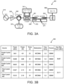
- FIG. 3 A is a simplified diagram illustrating a test vehicle setup using two acoustic resonator filter devices according to an example of the present invention.
- FIG. 3 B is a table comparing measurements of acoustic resonator devices according to various examples of the present invention using the test vehicle setup of FIG. 3 A .
- FIG. 4 is a simplified graph illustrating Time-To-Failure (TTF) versus power level for various acoustic resonator devices including examples according to the present invention.
- TTF Time-To-Failure
- FIG. 5 is a simplified graph illustrating power handling capability versus x-ray diffraction (XRD) rocking curve full width at half-maximum (FWHM) according to examples of the present invention.
- FIG. 6 A is a simplified diagram illustrating an acoustic resonator device having topside interconnections according to an example of the present invention.
- FIG. 6 B is a simplified diagram illustrating an acoustic resonator device having bottom-side interconnections according to an example of the present invention.
- the present invention provides techniques related to a method of manufacture and structure for bulk acoustic wave resonator devices, single crystal resonator devices, single crystal filter and resonator devices, and the like.
- the invention has been applied to a single crystal resonator device for a communication device, mobile device, computing device, among others.
- FIG. 1 is a simplified diagram illustrating an acoustic resonator device according to an example of the present invention.
- device 100 includes a substrate member 110 , a piezoelectric layer 120 , a bottom electrode 130 , and a top electrode 140 .
- the substrate member 110 includes a substrate surface region and an air cavity region 111 .
- the piezoelectric layer 120 is physically coupled to the substrate surface region and is spatially configured overlying the substrate member 110 and the air cavity region 111 .
- the piezoelectric layer 120 also includes a top piezo surface region and a bottom piezo surface region.
- the bottom electrode 130 is spatially configured underlying the piezoelectric layer 120 and physically coupled to the bottom piezo surface region. As shown in FIG.
- a gap 150 exists between the bottom electrode 130 and a portion of the substrate member 110 .
- the bottom electrode 130 can be patterned such that it is configured within the boundaries of the air cavity region 111 such that the bottom electrode 130 does not come in contact with one or more sidewalls of the substrate member 110 .
- the top electrode 140 is spatially configured overlying the piezoelectric layer 120 and physically coupled to the top piezo surface region.
- the substrate member 110 includes a silicon material, a silicon carbide (SiC) material, a ⁇ 111> orientation silicon material, or the like.
- the substrate member 110 can also include other substrate materials known by those of ordinary skill in the art.
- the bottom and top electrodes 130 , 140 can include common metal materials and alloys known by those of ordinary skill in the art.
- the piezoelectric layer 120 can include a single crystal material, a hybrid single crystal material, or a polycrystalline material, or the like.
- the piezoelectric layer 120 can also include a substantially single crystal material, i.e., an essentially single crystal material.
- the piezoelectric layer 120 can include an aluminum nitride (AlN) material, or the like.
- AlN aluminum nitride
- the piezoelectric layer 120 can be characterized by an x-ray rocking curve Full Width at Half Maximum (FWHM) ranging from 0 degrees to 2 degrees.
- FWHM Full Width at Half Maximum
- the piezoelectric layer 120 can also be characterized by a layer thickness of 500 nm.
- the layer thickness can be configured such that the piezoelectric layer 120 is characterized by an x-ray rocking curve FWHM ranging from 0 to 2 degrees.
- the configuration of the materials of the piezoelectric layer and the substrate member, including the layer thickness and materials, to achieve the x-ray rocking curve FWHM ranging from 0 to 2 degrees can improve a power handling capability characteristic and a power durability characteristic.
- the present invention provides a method of fabricating an acoustic resonator device.
- the method can include providing a substrate member and forming an air cavity within a portion of the substrate member.
- a piezoelectric layer can be physically coupled to a substrate region of the substrate member and spatially configured overlying the substrate member and the air cavity.
- a top electrode can be formed overlying the piezoelectric layer and physically coupled to a top piezo surface region of the piezoelectric layer.
- a bottom electrode can be formed underlying the piezoelectric layer and physically coupled to a bottom surface region of the piezoelectric layer.
- forming the piezoelectric layer includes forming a piezoelectric layer characterized by an x-ray rocking curve Full Width at Half Maximum (FWHM) ranging from 0 degrees to 2 degrees.
- FWHM Full Width at Half Maximum
- a thickness of the piezoelectric layer and material composition of the piezoelectric layer can be configured to achieve the FWHM values ranging from 0 degrees to 2 degrees.
- Examples of the present invention can be used on transmitter (Tx) and transceiver (Tx/Rx) applications.
- the device 100 can be configured in a Tx or Tx/Rx system where the acoustic wave RF filter is located after the power amplifier (PA).
- PA power amplifier
- the RF filter must function and survive the full output power of the PA.
- power handling capability and power durability are key characteristics to optimize in such applications.
- FIG. 2 is a table comparing acoustic resonator devices using different types of piezoelectric materials according to examples of the present invention.
- table 200 shows FWHM values in degrees and arcseconds for various types of piezoelectric material and substrate combinations at a piezoelectric layer thickness of 500 nm.
- the x-ray rocking curve FWHM parameter can depend on the combination of materials used for the piezoelectric layer and the substrate, as well as the thickness of these materials.
- an FWHM profile is used to characterize material properties and surface integrity features, and is an indicator of crystal quality.
- the results of table 200 show that the acoustic resonator devices using single crystal materials exhibit a lower FWHM compared to devices using polycrystalline material, i.e., single crystal materials have a higher crystal quality.
- FIG. 3 A is a simplified diagram illustrating a test vehicle setup using two acoustic resonator filter devices according to an example of the present invention.
- test vehicle 301 includes a signal generator 310 electrically coupled to a power amplifier 320 , which is electrically coupled to a circulator 330 .
- the circulator 330 is electrically coupled to a resistive load 331 , which is a 50 Ohm load in this example.
- the circulator 330 is electrically coupled to a coupler 340 , which is also electrically coupled to a power meter 341 .
- the power meter 341 can include a first channel (shown in FIG. 3 A as “Ch. A”) and a second channel (shown in FIG. 3 A as “Ch.
- the test vehicle 301 can also include a pair of wafer probes 351 , 352 configured such that the first wafer probe 351 is electrically coupled to the coupler 340 and the second wafer probe 352 is electrically coupled to a spectral analyzer 360 .
- a device under test (DUT) 371 is placed on a stage 372 and measured using the wafer probes 351 , 352 .
- the DUT 371 can include devices similar to those acoustic resonator devices discussed in reference to FIG. 1 .
- the DUT 371 used in the test vehicle 301 includes two resonator element filter devices.
- FIG. 3 B is a table comparing measurements of acoustic resonator devices according to various examples of the present invention using the test vehicle setup of FIG. 3 A .
- table 302 includes power measurements for acoustic resonator devices using single crystal AlN and poly-crystal AlN. These measurements were taken at an operating temperature of 25 degrees Celsius and performed using a Wideband Code Division Multiple Access (WCDMA) modulation at 5.2 GHz.
- WCDMA Wideband Code Division Multiple Access
- the acoustic resonator devices can be fabricated according to an XBAW stack process to form the device structure as shown in FIG. 1 . According to these test results, acoustic resonator devices according to examples of the present invention using single crystal piezoelectric materials show about a 3.7 dB higher average max power handling characteristic compared to those examples using polycrystalline piezoelectric materials.
- FIG. 4 is a simplified graph illustrating Time-To-Failure (TTF) versus power level for various acoustic resonator devices including examples according to the present invention.
- graph 400 includes curves approximating measurements for four devices.
- TTF decreases with increasing power drive.
- Curve 410 represents measurements for a thin-film bulk acoustic wave resonator (FBAR) device using polycrystalline AlN, tested at 70 degrees Celsius and at a frequency of 5 GHz.
- Curve 420 represents measurements for a surface acoustic resonator (SAW) device using a lithium tantalate (LiTaO 3 ) material, tested at room temperature and at a frequency of 2 GHz.
- FBAR thin-film bulk acoustic wave resonator
- SiTaO 3 lithium tantalate
- Curve 430 represents an acoustic resonator device according to an example of the present invention using polycrystalline AlN, tested at room temperature and at a frequency of 5.2 GHz.
- Curve 440 represents an acoustic resonator device according to an example of the present invention using single crystal AlN, tested at room temperature and at a frequency of 5.2 GHz.
- FIG. 5 is a simplified graph illustrating power handling capability versus x-ray diffraction (XRD) rocking curve full width at half-maximum (FWHM) according to examples of the present invention.
- graph 500 includes measurements for acoustic resonator devices according to examples of the present invention that use single crystal AlN based materials and examples that use polycrystalline AlN materials. These results show that single crystal AlN based materials exhibit a 2.3 times improvement over polycrystalline AlN based materials for power handling capability.
- the piezoelectric materials can be configured with XRD FWHM values up to 2 degrees in width, shown by region 510 , for improved power handling capability and power durability.
- FIG. 6 A is a simplified diagram illustrating an acoustic resonator device 601 having topside interconnections according to an example of the present invention.
- device 601 includes a thinned seed substrate 612 with an overlying single crystal piezoelectric layer 620 , which has a micro-via 629 .
- the micro-via 629 can include a topside micro-trench 621 , a topside metal plug 646 , a backside trench 614 , and a backside metal plug 647 .
- device 601 is depicted with a single micro-via 629 , device 601 may have multiple micro-vias.
- a topside metal electrode 630 is formed overlying the piezoelectric layer 620 .
- a top cap structure is bonded to the piezoelectric layer 620 .
- This top cap structure includes an interposer substrate 619 with one or more through-vias 651 that are connected to one or more top bond pads 643 , one or more bond pads 644 , and topside metal 645 with topside metal plug 646 .
- Solder balls 670 are electrically coupled to the one or more top bond pads 643 .
- the thinned substrate 612 has the first and second backside trenches 613 , 614 .
- a backside metal electrode 631 is formed underlying a portion of the thinned seed substrate 612 , the first backside trench 613 , and the topside metal electrode 630 .
- the backside metal plug 647 is formed underlying a portion of the thinned seed substrate 612 , the second backside trench 614 , and the topside metal 645 . This backside metal plug 647 is electrically coupled to the topside metal plug 646 and the backside metal electrode 631 .
- a backside cap structure 661 is bonded to the thinned seed substrate 612 , underlying the first and second backside trenches 613 , 614 .
- FIG. 6 B is a simplified diagram illustrating an acoustic resonator device 602 having backside interconnections according to an example of the present invention.
- device 601 includes a thinned seed substrate 612 with an overlying piezoelectric layer 620 , which has a micro-via 629 .
- the micro-via 629 can include a topside micro-trench 621 , a topside metal plug 646 , a backside trench 614 , and a backside metal plug 647 .
- device 602 is depicted with a single micro-via 629 , device 602 may have multiple micro-vias.
- a topside metal electrode 630 is formed overlying the piezoelectric layer 620 .
- a top cap structure is bonded to the piezoelectric layer 620 .
- This top cap structure 619 includes bond pads which are connected to one or more bond pads 644 and topside metal 645 on piezoelectric layer 620 .
- the topside metal 645 includes a topside metal plug 646 .
- the thinned substrate 612 has the first and second backside trenches 613 , 614 .
- a backside metal electrode 631 is formed underlying a portion of the thinned seed substrate 612 , the first backside trench 613 , and the topside metal electrode 630 .
- a backside metal plug 647 is formed underlying a portion of the thinned seed substrate 612 , the second backside trench 614 , and the topside metal plug 646 . This backside metal plug 647 is electrically coupled to the topside metal plug 646 .
- a backside cap structure 662 is bonded to the thinned seed substrate 612 , underlying the first and second backside trenches.
- One or more backside bond pads ( 671 , 672 , 673 ) are formed within one or more portions of the backside cap structure 662 .
- Solder balls 670 are electrically coupled to the one or more backside bond pads 671 - 673 .
- the device includes a seed substrate with a piezoelectric layer formed overlying.
- the seed substrate can include silicon, silicon carbide, aluminum oxide, or single crystal aluminum gallium nitride materials, or the like.
- the piezoelectric layer can include a piezoelectric single crystal layer or a thin film piezoelectric single crystal layer.
- the topside metal electrode can include a molybdenum, aluminum, ruthenium, or titanium material, or the like and combinations thereof.
- This layer can be deposited and patterned on top of the piezoelectric layer by a lift-off process, a wet etching process, a dry etching process, a metal printing process, a metal laminating process, or the like.
- the lift-off process can include a sequential process of lithographic patterning, metal deposition, and lift-off steps to produce the topside metal layer.
- the wet/dry etching processes can includes sequential processes of metal deposition, lithographic patterning, metal deposition, and metal etching steps to produce the topside metal layer.
- This topside micro-trench can serve as the main interconnect junction between the top and bottom sides of the acoustic membrane, which will be developed in later method steps.
- the topside micro-trench is extends all the way through the piezoelectric layer and stops in the seed substrate.
- This topside micro-trench can be formed through a dry etching process, a laser drilling process, or the like.
- a laser drill can be used to form nominal 50 um holes, or holes between 10 um and 500 um in diameter, through the piezoelectric layer and stop in the seed substrate below the interface between these layers.
- a protective layer can be formed overlying the piezoelectric layer and the topside metal electrode. This protective layer can serve to protect the device from laser debris and to provide a mask for the etching of the topside micro-via.
- the laser drill can be an 11 W high power diode-pumped UV laser, or the like. This mask can be subsequently removed before proceeding to other steps. The mask may also be omitted from the laser drilling process, and air flow can be used to remove laser debris.
- a lithographic masking layer can be forming overlying the piezoelectric layer and the topside metal electrode.
- the topside micro-trench can be formed by exposure to plasma, or the like.
- the topside metal can include a topside metal plug formed within the topside micro-trench.
- the topside metal plug fills the topside micro-trench to form a topside portion of a micro-via.
- the bond pads and the topside metal can include a gold material or other interconnect metal material depending upon the application of the device.
- These metal materials can be formed by a lift-off process, a wet etching process, a dry etching process, a screen-printing process, an electroplating process, a metal printing process, or the like.
- the deposited metal materials can also serve as bond pads for a cap structure, which will be described below.
- a top cap structure is positioned above the partially processed acoustic resonator device as described in the previous figures.
- the top cap structure can be formed using an interposer substrate in two configurations: fully processed interposer version (through glass via) and partially processed interposer version (blind via version).
- the interposer substrate includes through-via structures that extend through the interposer substrate and are electrically coupled to the bottom bond pads and the top bond pads.
- the interposer substrate includes blind via structures that only extend through a portion of the interposer substrate from the bottom side. These blind via structures are also electrically coupled to bottom bond pads.
- the interposer substrate can include a silicon, glass, smart-glass, or other like material.
- the interposer substrate is bonded to the piezoelectric layer by the bond pads and the topside metal.
- This bonding process can be done using a compression bond method or the like.
- this substrate thinning process can include grinding and etching processes or the like.
- this process can include a wafer backgrinding process followed by stress removal, which can involve dry etching, CMP polishing, or annealing processes.
- the first backside trench can be formed within the thinned seed substrate and underlying the topside metal electrode.
- the second backside trench can be formed within the thinned seed substrate and underlying the topside micro-trench and the topside metal plug.
- these trenches can be formed using deep reactive ion etching (DRIE) processes, Bosch processes, or the like.
- DRIE deep reactive ion etching
- the size, shape, and number of the trenches may vary with the design of the acoustic resonator device.
- the first backside trench may be formed with a trench shape similar to a shape of the topside metal electrode or a shape of the backside metal electrode.
- the first backside trench may also be formed with a trench shape that is different from both a shape of the topside metal electrode and the backside metal electrode.
- the backside metal electrode can be formed underlying one or more portions of the thinned substrate, within the first backside trench, and underlying the topside metal electrode. This process completes the resonator structure within the acoustic resonator device.
- the backside metal plug can be formed underlying one or more portions of the thinned substrate, within the second backside trench, and underlying the topside micro-trench.
- the backside metal plug can be electrically coupled to the topside metal plug and the backside metal electrode.
- the backside metal electrode can include a molybdenum, aluminum, ruthenium, or titanium material, or the like and combinations thereof.
- the backside metal plug can include a gold material, low resistivity interconnect metals, electrode metals, or the like. These layers can be deposited using the deposition methods described previously.
- the backside cap structure is a dry film cap, which can include a permanent photo-imageable dry film such as a solder mask, polyimide, or the like. Bonding this cap structure can be cost-effective and reliable, but may not produce a hermetic seal.
- the backside cap structure is a substrate, which can include a silicon, glass, or other like material. Bonding this substrate can provide a hermetic seal, but may cost more and require additional processes. Depending upon application, either of these backside cap structures can be bonded underlying the first and second backside vias.
- the packaged device can include any combination of elements described above, as well as outside of the present specification. Therefore, the above description and illustrations should not be taken as limiting the scope of the present invention which is defined by the appended claims.
Landscapes
- Physics & Mathematics (AREA)
- Acoustics & Sound (AREA)
- Engineering & Computer Science (AREA)
- Manufacturing & Machinery (AREA)
- Piezo-Electric Or Mechanical Vibrators, Or Delay Or Filter Circuits (AREA)
Abstract
Description
Claims (14)
Priority Applications (1)
| Application Number | Priority Date | Filing Date | Title |
|---|---|---|---|
| US16/552,999 US11652469B2 (en) | 2018-08-27 | 2019-08-27 | High power bulk acoustic wave resonator filter devices |
Applications Claiming Priority (2)
| Application Number | Priority Date | Filing Date | Title |
|---|---|---|---|
| US201862723152P | 2018-08-27 | 2018-08-27 | |
| US16/552,999 US11652469B2 (en) | 2018-08-27 | 2019-08-27 | High power bulk acoustic wave resonator filter devices |
Publications (2)
| Publication Number | Publication Date |
|---|---|
| US20200067486A1 US20200067486A1 (en) | 2020-02-27 |
| US11652469B2 true US11652469B2 (en) | 2023-05-16 |
Family
ID=69586489
Family Applications (1)
| Application Number | Title | Priority Date | Filing Date |
|---|---|---|---|
| US16/552,999 Active US11652469B2 (en) | 2018-08-27 | 2019-08-27 | High power bulk acoustic wave resonator filter devices |
Country Status (5)
| Country | Link |
|---|---|
| US (1) | US11652469B2 (en) |
| KR (1) | KR20210046062A (en) |
| CN (1) | CN112840562A (en) |
| DE (1) | DE112019004304T5 (en) |
| WO (1) | WO2020046995A1 (en) |
Cited By (1)
| Publication number | Priority date | Publication date | Assignee | Title |
|---|---|---|---|---|
| US20210273630A1 (en) * | 2020-05-18 | 2021-09-02 | Akoustis, Inc. | Bulk acoustic wave resonator filters including a high impedance shunt branch and methods of forming the same |
Families Citing this family (3)
| Publication number | Priority date | Publication date | Assignee | Title |
|---|---|---|---|---|
| DE112019004304T5 (en) * | 2018-08-27 | 2021-05-27 | Akoustis, Inc. | HIGH PERFORMANCE ACOUSTIC VOLUME WAVE RESONATOR FILTER DEVICES |
| CN111654259A (en) * | 2020-05-13 | 2020-09-11 | 深圳市信维通信股份有限公司 | Bulk acoustic wave resonance device, filtering device and radio frequency front end device |
| US20240333254A1 (en) * | 2021-07-19 | 2024-10-03 | Massachusetts Institute Of Technology | Single crystalline film bulk acoustic resonator and related systems and methods |
Citations (50)
| Publication number | Priority date | Publication date | Assignee | Title |
|---|---|---|---|---|
| US5231327A (en) | 1990-12-14 | 1993-07-27 | Tfr Technologies, Inc. | Optimized piezoelectric resonator-based networks |
| JPH09321361A (en) | 1996-05-27 | 1997-12-12 | Tdk Corp | Piezoelectric vibrator component and manufacture thereof |
| US5894647A (en) | 1997-06-30 | 1999-04-20 | Tfr Technologies, Inc. | Method for fabricating piezoelectric resonators and product |
| US6051907A (en) | 1996-10-10 | 2000-04-18 | Nokia Mobile Phones Limited | Method for performing on-wafer tuning of thin film bulk acoustic wave resonators (FBARS) |
| US6114635A (en) | 1998-07-14 | 2000-09-05 | Tfr Technologies, Inc. | Chip-scale electronic component package |
| US6262637B1 (en) | 1999-06-02 | 2001-07-17 | Agilent Technologies, Inc. | Duplexer incorporating thin-film bulk acoustic resonators (FBARs) |
| US6377137B1 (en) | 2000-09-11 | 2002-04-23 | Agilent Technologies, Inc. | Acoustic resonator filter with reduced electromagnetic influence due to die substrate thickness |
| US6384697B1 (en) | 2000-05-08 | 2002-05-07 | Agilent Technologies, Inc. | Cavity spanning bottom electrode of a substrate-mounted bulk wave acoustic resonator |
| US6472954B1 (en) | 2001-04-23 | 2002-10-29 | Agilent Technologies, Inc. | Controlled effective coupling coefficients for film bulk acoustic resonators |
| US6617060B2 (en) | 2000-12-14 | 2003-09-09 | Nitronex Corporation | Gallium nitride materials and methods |
| US6812619B1 (en) | 1999-07-19 | 2004-11-02 | Nokia Corporation | Resonator structure and a filter comprising such a resonator structure |
| US6841922B2 (en) | 2001-07-30 | 2005-01-11 | Infineon Technologies Ag | Piezoelectric resonator apparatus with acoustic reflector |
| US6864619B2 (en) | 2001-05-18 | 2005-03-08 | Infineon Technologies Ag | Piezoelectric resonator device having detuning layer sequence |
| US6879224B2 (en) | 2002-09-12 | 2005-04-12 | Agilent Technologies, Inc. | Integrated filter and impedance matching network |
| WO2005034349A1 (en) | 2003-10-06 | 2005-04-14 | Philips Intellectual Property & Standards Gmbh | Ladder-type thin-film bulk acoustic wave filter |
| US6909340B2 (en) | 2000-11-24 | 2005-06-21 | Infineon Technologies Ag | Bulk acoustic wave filter utilizing resonators with different aspect ratios |
| US6933807B2 (en) | 2002-11-07 | 2005-08-23 | Infineon Technologies Ag | Acoustic reflector for a BAW resonator providing specified reflection of both shear waves and longitudinal waves |
| US20050255234A1 (en) | 2004-04-23 | 2005-11-17 | Atsuhiko Kanda | Method for manufacturing resonator |
| US7112860B2 (en) | 2003-03-03 | 2006-09-26 | Cree, Inc. | Integrated nitride-based acoustic wave devices and methods of fabricating integrated nitride-based acoustic wave devices |
| CN1929302A (en) | 2005-09-09 | 2007-03-14 | 株式会社东芝 | Film bulk acoustic resonator and method for manufacturing the same |
| US20070080611A1 (en) | 2005-10-12 | 2007-04-12 | Ube Industries, Ltd. | Aluminum nitride thin film, composite film containing the same and piezoelectric thin film resonator using the same |
| US7250360B2 (en) | 2005-03-02 | 2007-07-31 | Cornell Research Foundation, Inc. | Single step, high temperature nucleation process for a lattice mismatched substrate |
| US7268436B2 (en) | 2003-03-10 | 2007-09-11 | Infineon Technologies Ag | Electronic device with cavity and a method for producing the same |
| US20080024042A1 (en) | 2006-07-31 | 2008-01-31 | Hitachi Media Electronics Co., Ltd. | Thin film piezoelectric bulk acoustic wave resonator and radio frequency filter using the same |
| US7365619B2 (en) | 2005-06-22 | 2008-04-29 | Infineon Technologies Ag | BAW apparatus |
| US20080284541A1 (en) | 2007-05-14 | 2008-11-20 | Cree, Inc. | Bulk acoustic device and method for fabricating |
| US20080284542A1 (en) * | 2006-10-25 | 2008-11-20 | Kabushiki Kaisha Toshiba | Film bulk acoustic resonator |
| US20090033177A1 (en) | 2005-08-08 | 2009-02-05 | Kabushiki Kaisha Toshiba | Thin film piezoelectric resonator and method of manufacturing the same |
| US7514759B1 (en) | 2004-04-19 | 2009-04-07 | Hrl Laboratories, Llc | Piezoelectric MEMS integration with GaN technology |
| JP2009100197A (en) | 2007-10-16 | 2009-05-07 | Renesas Technology Corp | Rf power amplifier apparatus, and power supply circuit to control power supply voltage of rf power amplifier |
| JP2010068109A (en) | 2008-09-09 | 2010-03-25 | Sumitomo Electric Ind Ltd | Surface acoustic wave element |
| US7777777B2 (en) | 2002-04-30 | 2010-08-17 | Tandberg Telecom As | System and method for active call monitoring |
| US8304271B2 (en) | 2009-05-20 | 2012-11-06 | Jenn Hwa Huang | Integrated circuit having a bulk acoustic wave device and a transistor |
| US20120287575A1 (en) | 2011-05-09 | 2012-11-15 | Bae Systems Information And Electronic Systems Integration Inc. | Module cooling method and plenum adaptor |
| US8405285B2 (en) * | 2009-06-08 | 2013-03-26 | Fujifilm Corporation | Piezoelectric device, piezoelectric actuator having the same, liquid discharge apparatus, and power generating apparatus |
| US20130176086A1 (en) | 2011-05-20 | 2013-07-11 | Avago Technologies General Ip (Singapore) Pte. Ltd. | Double bulk acoustic resonator comprising aluminum scandium nitride |
| US20140132117A1 (en) | 2010-01-22 | 2014-05-15 | Avago Technologies General Ip (Singapore) Pte. Ltd | Method of fabricating rare-earth doped piezoelectric material with various amounts of dopants and a selected c-axis orientation |
| US20150079329A1 (en) * | 2001-12-24 | 2015-03-19 | Crystal Is, Inc. | Method and apparatus for producing large, single-crystals of aluminum nitride |
| US20160028367A1 (en) | 2014-07-25 | 2016-01-28 | Akoustis, Inc. | Single crystal acoustic resonator and bulk acoustic wave filter |
| US20160036580A1 (en) | 2014-07-31 | 2016-02-04 | Akoustis, Inc. | Mobile communication device configured with a single crystal piezo resonator structure |
| WO2016122877A1 (en) | 2015-01-28 | 2016-08-04 | Qualcomm Incorporated | Power-saving mode fallback during concurrency scenarios |
| US20170264256A1 (en) | 2016-03-11 | 2017-09-14 | Akoustis, Inc. | Method of manufacture for single crystal acoustic resonator devices using micro-vias |
| WO2017171856A1 (en) | 2016-04-01 | 2017-10-05 | Intel Corporation | Inorganic piezoelectric materials formed on fibers & applications thereof |
| WO2017222990A1 (en) | 2016-06-19 | 2017-12-28 | IQE, plc | Epitaxial aln/rare earth oxide structure for rf filter applications |
| US20180275485A1 (en) * | 2017-03-24 | 2018-09-27 | Dror Hurwitz | Method of fabrication for single crystal piezoelectric rf resonators and filters |
| US20180323767A1 (en) * | 2015-12-04 | 2018-11-08 | Intel Corporation | Film bulk acoustic resonator (fbar) devices for high frequency rf filters |
| US20190199312A1 (en) * | 2016-09-30 | 2019-06-27 | Intel Corporation | Single-flipped resonator devices with 2deg bottom electrode |
| US20200067486A1 (en) * | 2018-08-27 | 2020-02-27 | Akoustis, Inc. | High power bulk acoustic wave resonator filter devices |
| US20200091406A1 (en) * | 2014-06-06 | 2020-03-19 | Akoustis, Inc. | Method of manufacture for single crystal capacitor dielectric for a resonance circuit |
| US20200343875A1 (en) * | 2018-06-01 | 2020-10-29 | Akoustis, Inc. | Effective coupling coefficients for strained single crystal epitaxial film bulk acoustic resonators |
Family Cites Families (3)
| Publication number | Priority date | Publication date | Assignee | Title |
|---|---|---|---|---|
| JP6166170B2 (en) * | 2013-12-16 | 2017-07-19 | 日本碍子株式会社 | Composite substrate and manufacturing method thereof |
| WO2016103925A1 (en) * | 2014-12-25 | 2016-06-30 | 株式会社村田製作所 | Elastic wave device and method for manufacturing same |
| CN107196618A (en) * | 2017-02-16 | 2017-09-22 | 杭州左蓝微电子技术有限公司 | FBAR and preparation method thereof |
-
2019
- 2019-08-27 DE DE112019004304.8T patent/DE112019004304T5/en not_active Withdrawn
- 2019-08-27 KR KR1020217008990A patent/KR20210046062A/en not_active Ceased
- 2019-08-27 CN CN201980067393.9A patent/CN112840562A/en active Pending
- 2019-08-27 US US16/552,999 patent/US11652469B2/en active Active
- 2019-08-27 WO PCT/US2019/048412 patent/WO2020046995A1/en not_active Ceased
Patent Citations (53)
| Publication number | Priority date | Publication date | Assignee | Title |
|---|---|---|---|---|
| US5231327A (en) | 1990-12-14 | 1993-07-27 | Tfr Technologies, Inc. | Optimized piezoelectric resonator-based networks |
| JPH09321361A (en) | 1996-05-27 | 1997-12-12 | Tdk Corp | Piezoelectric vibrator component and manufacture thereof |
| US6051907A (en) | 1996-10-10 | 2000-04-18 | Nokia Mobile Phones Limited | Method for performing on-wafer tuning of thin film bulk acoustic wave resonators (FBARS) |
| US5894647A (en) | 1997-06-30 | 1999-04-20 | Tfr Technologies, Inc. | Method for fabricating piezoelectric resonators and product |
| US6114635A (en) | 1998-07-14 | 2000-09-05 | Tfr Technologies, Inc. | Chip-scale electronic component package |
| US6262637B1 (en) | 1999-06-02 | 2001-07-17 | Agilent Technologies, Inc. | Duplexer incorporating thin-film bulk acoustic resonators (FBARs) |
| US6812619B1 (en) | 1999-07-19 | 2004-11-02 | Nokia Corporation | Resonator structure and a filter comprising such a resonator structure |
| US6384697B1 (en) | 2000-05-08 | 2002-05-07 | Agilent Technologies, Inc. | Cavity spanning bottom electrode of a substrate-mounted bulk wave acoustic resonator |
| US6377137B1 (en) | 2000-09-11 | 2002-04-23 | Agilent Technologies, Inc. | Acoustic resonator filter with reduced electromagnetic influence due to die substrate thickness |
| US6909340B2 (en) | 2000-11-24 | 2005-06-21 | Infineon Technologies Ag | Bulk acoustic wave filter utilizing resonators with different aspect ratios |
| US6617060B2 (en) | 2000-12-14 | 2003-09-09 | Nitronex Corporation | Gallium nitride materials and methods |
| US6472954B1 (en) | 2001-04-23 | 2002-10-29 | Agilent Technologies, Inc. | Controlled effective coupling coefficients for film bulk acoustic resonators |
| US6864619B2 (en) | 2001-05-18 | 2005-03-08 | Infineon Technologies Ag | Piezoelectric resonator device having detuning layer sequence |
| US6841922B2 (en) | 2001-07-30 | 2005-01-11 | Infineon Technologies Ag | Piezoelectric resonator apparatus with acoustic reflector |
| US20150079329A1 (en) * | 2001-12-24 | 2015-03-19 | Crystal Is, Inc. | Method and apparatus for producing large, single-crystals of aluminum nitride |
| US7777777B2 (en) | 2002-04-30 | 2010-08-17 | Tandberg Telecom As | System and method for active call monitoring |
| US6879224B2 (en) | 2002-09-12 | 2005-04-12 | Agilent Technologies, Inc. | Integrated filter and impedance matching network |
| US6933807B2 (en) | 2002-11-07 | 2005-08-23 | Infineon Technologies Ag | Acoustic reflector for a BAW resonator providing specified reflection of both shear waves and longitudinal waves |
| US7112860B2 (en) | 2003-03-03 | 2006-09-26 | Cree, Inc. | Integrated nitride-based acoustic wave devices and methods of fabricating integrated nitride-based acoustic wave devices |
| US20110114968A1 (en) | 2003-03-03 | 2011-05-19 | Sheppard Scott T | Integrated Nitride and Silicon Carbide-Based Devices |
| US7875910B2 (en) | 2003-03-03 | 2011-01-25 | Cree, Inc. | Integrated nitride and silicon carbide-based devices |
| US7268436B2 (en) | 2003-03-10 | 2007-09-11 | Infineon Technologies Ag | Electronic device with cavity and a method for producing the same |
| WO2005034349A1 (en) | 2003-10-06 | 2005-04-14 | Philips Intellectual Property & Standards Gmbh | Ladder-type thin-film bulk acoustic wave filter |
| US7514759B1 (en) | 2004-04-19 | 2009-04-07 | Hrl Laboratories, Llc | Piezoelectric MEMS integration with GaN technology |
| US20050255234A1 (en) | 2004-04-23 | 2005-11-17 | Atsuhiko Kanda | Method for manufacturing resonator |
| US7250360B2 (en) | 2005-03-02 | 2007-07-31 | Cornell Research Foundation, Inc. | Single step, high temperature nucleation process for a lattice mismatched substrate |
| US7365619B2 (en) | 2005-06-22 | 2008-04-29 | Infineon Technologies Ag | BAW apparatus |
| US20090033177A1 (en) | 2005-08-08 | 2009-02-05 | Kabushiki Kaisha Toshiba | Thin film piezoelectric resonator and method of manufacturing the same |
| CN1929302A (en) | 2005-09-09 | 2007-03-14 | 株式会社东芝 | Film bulk acoustic resonator and method for manufacturing the same |
| US20070080611A1 (en) | 2005-10-12 | 2007-04-12 | Ube Industries, Ltd. | Aluminum nitride thin film, composite film containing the same and piezoelectric thin film resonator using the same |
| US20080024042A1 (en) | 2006-07-31 | 2008-01-31 | Hitachi Media Electronics Co., Ltd. | Thin film piezoelectric bulk acoustic wave resonator and radio frequency filter using the same |
| US20080284542A1 (en) * | 2006-10-25 | 2008-11-20 | Kabushiki Kaisha Toshiba | Film bulk acoustic resonator |
| US7982363B2 (en) | 2007-05-14 | 2011-07-19 | Cree, Inc. | Bulk acoustic device and method for fabricating |
| US20080284541A1 (en) | 2007-05-14 | 2008-11-20 | Cree, Inc. | Bulk acoustic device and method for fabricating |
| JP2009100197A (en) | 2007-10-16 | 2009-05-07 | Renesas Technology Corp | Rf power amplifier apparatus, and power supply circuit to control power supply voltage of rf power amplifier |
| JP2010068109A (en) | 2008-09-09 | 2010-03-25 | Sumitomo Electric Ind Ltd | Surface acoustic wave element |
| US8304271B2 (en) | 2009-05-20 | 2012-11-06 | Jenn Hwa Huang | Integrated circuit having a bulk acoustic wave device and a transistor |
| US8405285B2 (en) * | 2009-06-08 | 2013-03-26 | Fujifilm Corporation | Piezoelectric device, piezoelectric actuator having the same, liquid discharge apparatus, and power generating apparatus |
| US20140132117A1 (en) | 2010-01-22 | 2014-05-15 | Avago Technologies General Ip (Singapore) Pte. Ltd | Method of fabricating rare-earth doped piezoelectric material with various amounts of dopants and a selected c-axis orientation |
| US20120287575A1 (en) | 2011-05-09 | 2012-11-15 | Bae Systems Information And Electronic Systems Integration Inc. | Module cooling method and plenum adaptor |
| US20130176086A1 (en) | 2011-05-20 | 2013-07-11 | Avago Technologies General Ip (Singapore) Pte. Ltd. | Double bulk acoustic resonator comprising aluminum scandium nitride |
| US20200091406A1 (en) * | 2014-06-06 | 2020-03-19 | Akoustis, Inc. | Method of manufacture for single crystal capacitor dielectric for a resonance circuit |
| US20160028367A1 (en) | 2014-07-25 | 2016-01-28 | Akoustis, Inc. | Single crystal acoustic resonator and bulk acoustic wave filter |
| US20160036580A1 (en) | 2014-07-31 | 2016-02-04 | Akoustis, Inc. | Mobile communication device configured with a single crystal piezo resonator structure |
| WO2016122877A1 (en) | 2015-01-28 | 2016-08-04 | Qualcomm Incorporated | Power-saving mode fallback during concurrency scenarios |
| US20180323767A1 (en) * | 2015-12-04 | 2018-11-08 | Intel Corporation | Film bulk acoustic resonator (fbar) devices for high frequency rf filters |
| US20170264256A1 (en) | 2016-03-11 | 2017-09-14 | Akoustis, Inc. | Method of manufacture for single crystal acoustic resonator devices using micro-vias |
| WO2017171856A1 (en) | 2016-04-01 | 2017-10-05 | Intel Corporation | Inorganic piezoelectric materials formed on fibers & applications thereof |
| WO2017222990A1 (en) | 2016-06-19 | 2017-12-28 | IQE, plc | Epitaxial aln/rare earth oxide structure for rf filter applications |
| US20190199312A1 (en) * | 2016-09-30 | 2019-06-27 | Intel Corporation | Single-flipped resonator devices with 2deg bottom electrode |
| US20180275485A1 (en) * | 2017-03-24 | 2018-09-27 | Dror Hurwitz | Method of fabrication for single crystal piezoelectric rf resonators and filters |
| US20200343875A1 (en) * | 2018-06-01 | 2020-10-29 | Akoustis, Inc. | Effective coupling coefficients for strained single crystal epitaxial film bulk acoustic resonators |
| US20200067486A1 (en) * | 2018-08-27 | 2020-02-27 | Akoustis, Inc. | High power bulk acoustic wave resonator filter devices |
Non-Patent Citations (5)
| Title |
|---|
| International Search Report and Written Opinion for PCT/US2015/034560, dated Sep. 18, 2015. |
| International Search Report and Written Opinion for PCT/US2018/050521, dated Jan. 28, 2019. |
| International Search Report and Written Opinion for PCT/US2019/018550, dated May 30, 2019. |
| International Search Report and Written Opinion for PCT/US2019/048412, dated Nov. 19, 2019. |
| Office Action dated Sep. 17, 2018 for Chinese Application No. 201580042442.5. |
Cited By (2)
| Publication number | Priority date | Publication date | Assignee | Title |
|---|---|---|---|---|
| US20210273630A1 (en) * | 2020-05-18 | 2021-09-02 | Akoustis, Inc. | Bulk acoustic wave resonator filters including a high impedance shunt branch and methods of forming the same |
| US12028046B2 (en) * | 2020-05-18 | 2024-07-02 | Akoustis, Inc. | Bulk acoustic wave resonator filters including a high impedance shunt branch and methods of forming the same |
Also Published As
| Publication number | Publication date |
|---|---|
| US20200067486A1 (en) | 2020-02-27 |
| CN112840562A (en) | 2021-05-25 |
| WO2020046995A1 (en) | 2020-03-05 |
| DE112019004304T5 (en) | 2021-05-27 |
| KR20210046062A (en) | 2021-04-27 |
Similar Documents
| Publication | Publication Date | Title |
|---|---|---|
| US10979025B2 (en) | 5G band n79 acoustic wave resonator RF filter circuit | |
| US10355659B2 (en) | Piezoelectric acoustic resonator manufactured with piezoelectric thin film transfer process | |
| US11031989B2 (en) | Front end module for 5.2 GHz Wi-Fi acoustic wave resonator RF filter circuit | |
| US10979022B2 (en) | 5.2 GHz Wi-Fi acoustic wave resonator RF filter circuit | |
| US20220345111A1 (en) | 5G n41 2.6 GHz BAND ACOUSTIC WAVE RESONATOR RF FILTER CIRCUIT | |
| US10979026B2 (en) | 5.5 GHz Wi-fi 5G coexistence acoustic wave resonator RF filter circuit | |
| US10985732B2 (en) | 5.6 GHz Wi-Fi acoustic wave resonator RF filter circuit | |
| US11711064B2 (en) | Acoustic wave resonator, RF filter circuit and system | |
| US11637545B2 (en) | Acoustic wave resonator RF filter circuit and system | |
| US11652469B2 (en) | High power bulk acoustic wave resonator filter devices | |
| US10979023B2 (en) | 5.9 GHz c-V2X and DSRC acoustic wave resonator RF filter circuit | |
| US11070184B2 (en) | Piezoelectric acoustic resonator manufactured with piezoelectric thin film transfer process | |
| US20230412145A1 (en) | Method and structure for high performance resonance circuit with single crystal piezoelectric capacitor dielectric material | |
| US20190326885A1 (en) | 5g 3.5-3.6ghz band acoustic wave resonator rf filter circuit | |
| US20210234525A1 (en) | Piezoelectric acoustic resonator with dielectric protective layer manufactured with piezoelectric thin film transfer process | |
| US20220263484A1 (en) | Piezoelectric acoustic resonator with improved tcf manufactured with piezoelectric thin film transfer process | |
| US20200228096A1 (en) | 5.5 GHz Wi-Fi 5G COEXISTENCE ACOUSTIC WAVE RESONATOR RF FILTER CIRCUIT | |
| US20220166408A1 (en) | Acoustic wave resonator rf filter circuit device | |
| US20240154602A9 (en) | Bulk acoustic wave resonator filters including a high impedance shunt branch and methods of forming the same | |
| WO2020006578A1 (en) | 5G 3.5-3.6 GHz BAND ACOUSTIC WAVE RESONATOR RF FILTER CIRCUIT | |
| US11683021B2 (en) | 4.5G 3.55-3.7 GHz band bulk acoustic wave resonator RF filter circuit |
Legal Events
| Date | Code | Title | Description |
|---|---|---|---|
| FEPP | Fee payment procedure |
Free format text: ENTITY STATUS SET TO UNDISCOUNTED (ORIGINAL EVENT CODE: BIG.); ENTITY STATUS OF PATENT OWNER: LARGE ENTITY |
|
| STPP | Information on status: patent application and granting procedure in general |
Free format text: APPLICATION DISPATCHED FROM PREEXAM, NOT YET DOCKETED |
|
| STPP | Information on status: patent application and granting procedure in general |
Free format text: DOCKETED NEW CASE - READY FOR EXAMINATION |
|
| STPP | Information on status: patent application and granting procedure in general |
Free format text: NON FINAL ACTION MAILED |
|
| STPP | Information on status: patent application and granting procedure in general |
Free format text: RESPONSE TO NON-FINAL OFFICE ACTION ENTERED AND FORWARDED TO EXAMINER |
|
| STPP | Information on status: patent application and granting procedure in general |
Free format text: FINAL REJECTION MAILED |
|
| STPP | Information on status: patent application and granting procedure in general |
Free format text: DOCKETED NEW CASE - READY FOR EXAMINATION |
|
| STPP | Information on status: patent application and granting procedure in general |
Free format text: NON FINAL ACTION MAILED |
|
| AS | Assignment |
Owner name: AKOUSTIS, INC., NORTH CAROLINA Free format text: ASSIGNMENT OF ASSIGNORS INTEREST;ASSIGNORS:SHEALY, JEFFREY B.;GIBB, SHAWN R.;HOULDEN, ROHAN W.;AND OTHERS;SIGNING DATES FROM 20200713 TO 20220602;REEL/FRAME:060192/0491 |
|
| STPP | Information on status: patent application and granting procedure in general |
Free format text: RESPONSE TO NON-FINAL OFFICE ACTION ENTERED AND FORWARDED TO EXAMINER |
|
| STPP | Information on status: patent application and granting procedure in general |
Free format text: FINAL REJECTION MAILED |
|
| STPP | Information on status: patent application and granting procedure in general |
Free format text: DOCKETED NEW CASE - READY FOR EXAMINATION |
|
| STCF | Information on status: patent grant |
Free format text: PATENTED CASE |
|
| AS | Assignment |
Owner name: TUNE HOLDINGS CORP., CALIFORNIA Free format text: ASSIGNMENT OF ASSIGNORS INTEREST;ASSIGNORS:AKOUSTIS TECHNOLOGIES, INC.;AKOUSTIS, INC.;RFM INTEGRATED DEVICE INC.;REEL/FRAME:071577/0023 Effective date: 20250515 Owner name: TUNE HOLDINGS CORP., CALIFORNIA Free format text: ASSIGNMENT OF ASSIGNOR'S INTEREST;ASSIGNORS:AKOUSTIS TECHNOLOGIES, INC.;AKOUSTIS, INC.;RFM INTEGRATED DEVICE INC.;REEL/FRAME:071577/0023 Effective date: 20250515 Owner name: AKOUSTIS TECHNOLOGIES CORP., NORTH CAROLINA Free format text: CHANGE OF NAME;ASSIGNOR:TUNE HOLDINGS CORP.;REEL/FRAME:071782/0456 Effective date: 20250515 |