US11652396B2 - DC-DC resonant converter and control method thereof - Google Patents
DC-DC resonant converter and control method thereof Download PDFInfo
- Publication number
- US11652396B2 US11652396B2 US17/363,119 US202117363119A US11652396B2 US 11652396 B2 US11652396 B2 US 11652396B2 US 202117363119 A US202117363119 A US 202117363119A US 11652396 B2 US11652396 B2 US 11652396B2
- Authority
- US
- United States
- Prior art keywords
- secondary side
- bridge rectifier
- leg
- cells
- serial
- Prior art date
- Legal status (The legal status is an assumption and is not a legal conclusion. Google has not performed a legal analysis and makes no representation as to the accuracy of the status listed.)
- Active
Links
Images


Classifications
-
- H—ELECTRICITY
- H02—GENERATION; CONVERSION OR DISTRIBUTION OF ELECTRIC POWER
- H02M—APPARATUS FOR CONVERSION BETWEEN AC AND AC, BETWEEN AC AND DC, OR BETWEEN DC AND DC, AND FOR USE WITH MAINS OR SIMILAR POWER SUPPLY SYSTEMS; CONVERSION OF DC OR AC INPUT POWER INTO SURGE OUTPUT POWER; CONTROL OR REGULATION THEREOF
- H02M3/00—Conversion of dc power input into dc power output
- H02M3/22—Conversion of dc power input into dc power output with intermediate conversion into ac
- H02M3/24—Conversion of dc power input into dc power output with intermediate conversion into ac by static converters
- H02M3/28—Conversion of dc power input into dc power output with intermediate conversion into ac by static converters using discharge tubes with control electrode or semiconductor devices with control electrode to produce the intermediate ac
- H02M3/325—Conversion of dc power input into dc power output with intermediate conversion into ac by static converters using discharge tubes with control electrode or semiconductor devices with control electrode to produce the intermediate ac using devices of a triode or a transistor type requiring continuous application of a control signal
- H02M3/335—Conversion of dc power input into dc power output with intermediate conversion into ac by static converters using discharge tubes with control electrode or semiconductor devices with control electrode to produce the intermediate ac using devices of a triode or a transistor type requiring continuous application of a control signal using semiconductor devices only
- H02M3/33569—Conversion of dc power input into dc power output with intermediate conversion into ac by static converters using discharge tubes with control electrode or semiconductor devices with control electrode to produce the intermediate ac using devices of a triode or a transistor type requiring continuous application of a control signal using semiconductor devices only having several active switching elements
-
- H—ELECTRICITY
- H02—GENERATION; CONVERSION OR DISTRIBUTION OF ELECTRIC POWER
- H02M—APPARATUS FOR CONVERSION BETWEEN AC AND AC, BETWEEN AC AND DC, OR BETWEEN DC AND DC, AND FOR USE WITH MAINS OR SIMILAR POWER SUPPLY SYSTEMS; CONVERSION OF DC OR AC INPUT POWER INTO SURGE OUTPUT POWER; CONTROL OR REGULATION THEREOF
- H02M1/00—Details of apparatus for conversion
- H02M1/0067—Converter structures employing plural converter units, other than for parallel operation of the units on a single load
- H02M1/0074—Plural converter units whose inputs are connected in series
-
- H—ELECTRICITY
- H02—GENERATION; CONVERSION OR DISTRIBUTION OF ELECTRIC POWER
- H02M—APPARATUS FOR CONVERSION BETWEEN AC AND AC, BETWEEN AC AND DC, OR BETWEEN DC AND DC, AND FOR USE WITH MAINS OR SIMILAR POWER SUPPLY SYSTEMS; CONVERSION OF DC OR AC INPUT POWER INTO SURGE OUTPUT POWER; CONTROL OR REGULATION THEREOF
- H02M3/00—Conversion of dc power input into dc power output
- H02M3/01—Resonant DC/DC converters
-
- H—ELECTRICITY
- H02—GENERATION; CONVERSION OR DISTRIBUTION OF ELECTRIC POWER
- H02M—APPARATUS FOR CONVERSION BETWEEN AC AND AC, BETWEEN AC AND DC, OR BETWEEN DC AND DC, AND FOR USE WITH MAINS OR SIMILAR POWER SUPPLY SYSTEMS; CONVERSION OF DC OR AC INPUT POWER INTO SURGE OUTPUT POWER; CONTROL OR REGULATION THEREOF
- H02M3/00—Conversion of dc power input into dc power output
- H02M3/22—Conversion of dc power input into dc power output with intermediate conversion into ac
- H02M3/24—Conversion of dc power input into dc power output with intermediate conversion into ac by static converters
- H02M3/28—Conversion of dc power input into dc power output with intermediate conversion into ac by static converters using discharge tubes with control electrode or semiconductor devices with control electrode to produce the intermediate ac
- H02M3/325—Conversion of dc power input into dc power output with intermediate conversion into ac by static converters using discharge tubes with control electrode or semiconductor devices with control electrode to produce the intermediate ac using devices of a triode or a transistor type requiring continuous application of a control signal
- H02M3/335—Conversion of dc power input into dc power output with intermediate conversion into ac by static converters using discharge tubes with control electrode or semiconductor devices with control electrode to produce the intermediate ac using devices of a triode or a transistor type requiring continuous application of a control signal using semiconductor devices only
- H02M3/33569—Conversion of dc power input into dc power output with intermediate conversion into ac by static converters using discharge tubes with control electrode or semiconductor devices with control electrode to produce the intermediate ac using devices of a triode or a transistor type requiring continuous application of a control signal using semiconductor devices only having several active switching elements
- H02M3/33571—Half-bridge at primary side of an isolation transformer
-
- H—ELECTRICITY
- H02—GENERATION; CONVERSION OR DISTRIBUTION OF ELECTRIC POWER
- H02M—APPARATUS FOR CONVERSION BETWEEN AC AND AC, BETWEEN AC AND DC, OR BETWEEN DC AND DC, AND FOR USE WITH MAINS OR SIMILAR POWER SUPPLY SYSTEMS; CONVERSION OF DC OR AC INPUT POWER INTO SURGE OUTPUT POWER; CONTROL OR REGULATION THEREOF
- H02M3/00—Conversion of dc power input into dc power output
- H02M3/22—Conversion of dc power input into dc power output with intermediate conversion into ac
- H02M3/24—Conversion of dc power input into dc power output with intermediate conversion into ac by static converters
- H02M3/28—Conversion of dc power input into dc power output with intermediate conversion into ac by static converters using discharge tubes with control electrode or semiconductor devices with control electrode to produce the intermediate ac
- H02M3/325—Conversion of dc power input into dc power output with intermediate conversion into ac by static converters using discharge tubes with control electrode or semiconductor devices with control electrode to produce the intermediate ac using devices of a triode or a transistor type requiring continuous application of a control signal
- H02M3/335—Conversion of dc power input into dc power output with intermediate conversion into ac by static converters using discharge tubes with control electrode or semiconductor devices with control electrode to produce the intermediate ac using devices of a triode or a transistor type requiring continuous application of a control signal using semiconductor devices only
- H02M3/33569—Conversion of dc power input into dc power output with intermediate conversion into ac by static converters using discharge tubes with control electrode or semiconductor devices with control electrode to produce the intermediate ac using devices of a triode or a transistor type requiring continuous application of a control signal using semiconductor devices only having several active switching elements
- H02M3/33576—Conversion of dc power input into dc power output with intermediate conversion into ac by static converters using discharge tubes with control electrode or semiconductor devices with control electrode to produce the intermediate ac using devices of a triode or a transistor type requiring continuous application of a control signal using semiconductor devices only having several active switching elements having at least one active switching element at the secondary side of an isolation transformer
- H02M3/33592—Conversion of dc power input into dc power output with intermediate conversion into ac by static converters using discharge tubes with control electrode or semiconductor devices with control electrode to produce the intermediate ac using devices of a triode or a transistor type requiring continuous application of a control signal using semiconductor devices only having several active switching elements having at least one active switching element at the secondary side of an isolation transformer having a synchronous rectifier circuit or a synchronous freewheeling circuit at the secondary side of an isolation transformer
-
- H—ELECTRICITY
- H02—GENERATION; CONVERSION OR DISTRIBUTION OF ELECTRIC POWER
- H02M—APPARATUS FOR CONVERSION BETWEEN AC AND AC, BETWEEN AC AND DC, OR BETWEEN DC AND DC, AND FOR USE WITH MAINS OR SIMILAR POWER SUPPLY SYSTEMS; CONVERSION OF DC OR AC INPUT POWER INTO SURGE OUTPUT POWER; CONTROL OR REGULATION THEREOF
- H02M7/00—Conversion of ac power input into dc power output; Conversion of dc power input into ac power output
- H02M7/02—Conversion of ac power input into dc power output without possibility of reversal
- H02M7/04—Conversion of ac power input into dc power output without possibility of reversal by static converters
- H02M7/06—Conversion of ac power input into dc power output without possibility of reversal by static converters using discharge tubes without control electrode or semiconductor devices without control electrode
-
- H—ELECTRICITY
- H02—GENERATION; CONVERSION OR DISTRIBUTION OF ELECTRIC POWER
- H02M—APPARATUS FOR CONVERSION BETWEEN AC AND AC, BETWEEN AC AND DC, OR BETWEEN DC AND DC, AND FOR USE WITH MAINS OR SIMILAR POWER SUPPLY SYSTEMS; CONVERSION OF DC OR AC INPUT POWER INTO SURGE OUTPUT POWER; CONTROL OR REGULATION THEREOF
- H02M7/00—Conversion of ac power input into dc power output; Conversion of dc power input into ac power output
- H02M7/42—Conversion of dc power input into ac power output without possibility of reversal
- H02M7/44—Conversion of dc power input into ac power output without possibility of reversal by static converters
- H02M7/48—Conversion of dc power input into ac power output without possibility of reversal by static converters using discharge tubes with control electrode or semiconductor devices with control electrode
- H02M7/53—Conversion of dc power input into ac power output without possibility of reversal by static converters using discharge tubes with control electrode or semiconductor devices with control electrode using devices of a triode or transistor type requiring continuous application of a control signal
- H02M7/537—Conversion of dc power input into ac power output without possibility of reversal by static converters using discharge tubes with control electrode or semiconductor devices with control electrode using devices of a triode or transistor type requiring continuous application of a control signal using semiconductor devices only, e.g. single switched pulse inverters
- H02M7/5387—Conversion of dc power input into ac power output without possibility of reversal by static converters using discharge tubes with control electrode or semiconductor devices with control electrode using devices of a triode or transistor type requiring continuous application of a control signal using semiconductor devices only, e.g. single switched pulse inverters in a bridge configuration
- H02M7/53871—Conversion of dc power input into ac power output without possibility of reversal by static converters using discharge tubes with control electrode or semiconductor devices with control electrode using devices of a triode or transistor type requiring continuous application of a control signal using semiconductor devices only, e.g. single switched pulse inverters in a bridge configuration with automatic control of output voltage or current
-
- H—ELECTRICITY
- H02—GENERATION; CONVERSION OR DISTRIBUTION OF ELECTRIC POWER
- H02M—APPARATUS FOR CONVERSION BETWEEN AC AND AC, BETWEEN AC AND DC, OR BETWEEN DC AND DC, AND FOR USE WITH MAINS OR SIMILAR POWER SUPPLY SYSTEMS; CONVERSION OF DC OR AC INPUT POWER INTO SURGE OUTPUT POWER; CONTROL OR REGULATION THEREOF
- H02M1/00—Details of apparatus for conversion
- H02M1/0003—Details of control, feedback or regulation circuits
- H02M1/0009—Devices or circuits for detecting current in a converter
-
- H—ELECTRICITY
- H02—GENERATION; CONVERSION OR DISTRIBUTION OF ELECTRIC POWER
- H02M—APPARATUS FOR CONVERSION BETWEEN AC AND AC, BETWEEN AC AND DC, OR BETWEEN DC AND DC, AND FOR USE WITH MAINS OR SIMILAR POWER SUPPLY SYSTEMS; CONVERSION OF DC OR AC INPUT POWER INTO SURGE OUTPUT POWER; CONTROL OR REGULATION THEREOF
- H02M1/00—Details of apparatus for conversion
- H02M1/0048—Circuits or arrangements for reducing losses
- H02M1/0054—Transistor switching losses
- H02M1/0058—Transistor switching losses by employing soft switching techniques, i.e. commutation of transistors when applied voltage is zero or when current flow is zero
-
- H—ELECTRICITY
- H02—GENERATION; CONVERSION OR DISTRIBUTION OF ELECTRIC POWER
- H02M—APPARATUS FOR CONVERSION BETWEEN AC AND AC, BETWEEN AC AND DC, OR BETWEEN DC AND DC, AND FOR USE WITH MAINS OR SIMILAR POWER SUPPLY SYSTEMS; CONVERSION OF DC OR AC INPUT POWER INTO SURGE OUTPUT POWER; CONTROL OR REGULATION THEREOF
- H02M3/00—Conversion of dc power input into dc power output
- H02M3/22—Conversion of dc power input into dc power output with intermediate conversion into ac
- H02M3/24—Conversion of dc power input into dc power output with intermediate conversion into ac by static converters
- H02M3/28—Conversion of dc power input into dc power output with intermediate conversion into ac by static converters using discharge tubes with control electrode or semiconductor devices with control electrode to produce the intermediate ac
- H02M3/325—Conversion of dc power input into dc power output with intermediate conversion into ac by static converters using discharge tubes with control electrode or semiconductor devices with control electrode to produce the intermediate ac using devices of a triode or a transistor type requiring continuous application of a control signal
- H02M3/335—Conversion of dc power input into dc power output with intermediate conversion into ac by static converters using discharge tubes with control electrode or semiconductor devices with control electrode to produce the intermediate ac using devices of a triode or a transistor type requiring continuous application of a control signal using semiconductor devices only
- H02M3/33569—Conversion of dc power input into dc power output with intermediate conversion into ac by static converters using discharge tubes with control electrode or semiconductor devices with control electrode to produce the intermediate ac using devices of a triode or a transistor type requiring continuous application of a control signal using semiconductor devices only having several active switching elements
- H02M3/33573—Full-bridge at primary side of an isolation transformer
-
- H—ELECTRICITY
- H02—GENERATION; CONVERSION OR DISTRIBUTION OF ELECTRIC POWER
- H02M—APPARATUS FOR CONVERSION BETWEEN AC AND AC, BETWEEN AC AND DC, OR BETWEEN DC AND DC, AND FOR USE WITH MAINS OR SIMILAR POWER SUPPLY SYSTEMS; CONVERSION OF DC OR AC INPUT POWER INTO SURGE OUTPUT POWER; CONTROL OR REGULATION THEREOF
- H02M3/00—Conversion of dc power input into dc power output
- H02M3/22—Conversion of dc power input into dc power output with intermediate conversion into ac
- H02M3/24—Conversion of dc power input into dc power output with intermediate conversion into ac by static converters
- H02M3/28—Conversion of dc power input into dc power output with intermediate conversion into ac by static converters using discharge tubes with control electrode or semiconductor devices with control electrode to produce the intermediate ac
- H02M3/325—Conversion of dc power input into dc power output with intermediate conversion into ac by static converters using discharge tubes with control electrode or semiconductor devices with control electrode to produce the intermediate ac using devices of a triode or a transistor type requiring continuous application of a control signal
- H02M3/335—Conversion of dc power input into dc power output with intermediate conversion into ac by static converters using discharge tubes with control electrode or semiconductor devices with control electrode to produce the intermediate ac using devices of a triode or a transistor type requiring continuous application of a control signal using semiconductor devices only
- H02M3/33569—Conversion of dc power input into dc power output with intermediate conversion into ac by static converters using discharge tubes with control electrode or semiconductor devices with control electrode to produce the intermediate ac using devices of a triode or a transistor type requiring continuous application of a control signal using semiconductor devices only having several active switching elements
- H02M3/33576—Conversion of dc power input into dc power output with intermediate conversion into ac by static converters using discharge tubes with control electrode or semiconductor devices with control electrode to produce the intermediate ac using devices of a triode or a transistor type requiring continuous application of a control signal using semiconductor devices only having several active switching elements having at least one active switching element at the secondary side of an isolation transformer
- H02M3/33584—Bidirectional converters
-
- Y—GENERAL TAGGING OF NEW TECHNOLOGICAL DEVELOPMENTS; GENERAL TAGGING OF CROSS-SECTIONAL TECHNOLOGIES SPANNING OVER SEVERAL SECTIONS OF THE IPC; TECHNICAL SUBJECTS COVERED BY FORMER USPC CROSS-REFERENCE ART COLLECTIONS [XRACs] AND DIGESTS
- Y02—TECHNOLOGIES OR APPLICATIONS FOR MITIGATION OR ADAPTATION AGAINST CLIMATE CHANGE
- Y02B—CLIMATE CHANGE MITIGATION TECHNOLOGIES RELATED TO BUILDINGS, e.g. HOUSING, HOUSE APPLIANCES OR RELATED END-USER APPLICATIONS
- Y02B70/00—Technologies for an efficient end-user side electric power management and consumption
- Y02B70/10—Technologies improving the efficiency by using switched-mode power supplies [SMPS], i.e. efficient power electronics conversion e.g. power factor correction or reduction of losses in power supplies or efficient standby modes
-
- Y—GENERAL TAGGING OF NEW TECHNOLOGICAL DEVELOPMENTS; GENERAL TAGGING OF CROSS-SECTIONAL TECHNOLOGIES SPANNING OVER SEVERAL SECTIONS OF THE IPC; TECHNICAL SUBJECTS COVERED BY FORMER USPC CROSS-REFERENCE ART COLLECTIONS [XRACs] AND DIGESTS
- Y02—TECHNOLOGIES OR APPLICATIONS FOR MITIGATION OR ADAPTATION AGAINST CLIMATE CHANGE
- Y02P—CLIMATE CHANGE MITIGATION TECHNOLOGIES IN THE PRODUCTION OR PROCESSING OF GOODS
- Y02P80/00—Climate change mitigation technologies for sector-wide applications
- Y02P80/10—Efficient use of energy, e.g. using compressed air or pressurized fluid as energy carrier
Definitions
- This present disclosure relates to a DC-DC resonant converter and a control method thereof. More particularly, the present disclosure relates to a stacked-bridge resonant converter with switching frequency control and voltage balancing strategies.
- the resonant converter which employ a resonant-tank circuit to shape the switch voltage and/or current waveforms to minimize switching losses and allow high-frequency operation, has been widely employed as an isolated DC/DC converter, due to its high efficiency, simple structure achieved by magnetic integration, soft switching on both primary and secondary switches, and capability suitable for applications with wide voltage ranges.
- FIGS. 1 A and 1 B respectively show a conventional full-bridge LLC resonant converter under closed-loop voltage control and the timing diagrams of control signals for switches S 1 to S 4 and a primary-side full-bridge output voltage V AB .
- Output voltage V AB may be regulated by controlling the switching frequency of these primary-side switches.
- Highest efficiency is attained when the LLC resonant converter operates at resonant frequency f r , determined by resonant inductor L r and resonant capacitor Cr, and when DC voltage gain M equals the transformer's turns ratio N P /N S .
- DC voltage gain M diminishes when switching frequency f sw is greater than resonant frequency f r .
- gain M becomes greater when switching frequency f sw is less than resonant frequency f r .
- Efficiency however, always diminishes as switching frequency f sw moves away from resonant frequency f r .
- the LLC resonant converter should operate at its corresponding frequency range.
- the resonant tank includes inductor L r and capacitors Cr connected in series, and the circuit can be referred to as a series-resonant converter.
- the magnetizing inductance L m of transformer TR is relatively small, i.e., if it is only several times of resonant inductance L r , the converter can operate as an LLC series-resonant converter.
- the secondary-side diode rectifier (including diodes D 1 , D 2 , D 3 , and D 4 ) can be implemented by a synchronous rectifier (e.g., using low on-resistance MOSFETs) to improve the efficiency.
- This implementation also makes the converter bidirectional, because controllable switches on both sides of the transformer allow power to flow in both directions. It should also be noted that the secondary-side of the isolated resonant converter can be implemented with a center-tapped secondary side winding instead of employing a full-wave rectifier as shown in FIG. 1 A .
- resonant converters are controlled by variable switching-frequency control.
- ZVS zero-voltage-switching
- ZCS zero-current switching
- FIG. 1 B Typical timing diagrams of switch-control signals for the series-resonant converter in FIG. 1 A operating with ZVS are shown in FIG. 1 B .
- all switches S 1 , S 2 , S 3 , and S 4 operate with the same duty ratio of 50%.
- the primary side switches in the same leg i.e., switches S 1 and S 2 in leg A and switches S 3 and S 4 in leg B
- the frequency of the primary side switches is determined by a feedback control loop that is employed to regulate the output.
- the duty ratios of the primary switches are set to a value slightly less than 50% by introducing a short delay (or dead time) between the turn-off and the turn on of the complementary operated same-leg switches. During this dead time, the current is commutated from the switch of the device that is being turned off to the antiparallel diode of the other device which creates a condition for its subsequent ZVS turn on.
- the full bridge structure is normally used in less than 800V DC input voltage applications when 1.2 kV devices are applied.
- three-level topology in Ref. [2] is more attractive, because of the fact that each switching device needs to block only one half of the input voltage.
- Three-level topology is applied to LLC converters in Ref [3], in which the proposed converters achieve ZVS for the switches without additional auxiliary circuit.
- Ref. [4] a three-level serial half bridge (SHB) topology, also known as stacked buck topology, is proposed for the first time. This topology removes the two clamping diodes in comparison with the conventional three-level topology from Ref. [2].
- SHB three-level serial half bridge
- FIGS. 2 A and 2 B respectively illustrate an exemplary serial half bridge resonant converter and its timing diagrams of control signals for switches S 1 to S 4 and a primary-side full-bridge output voltage V AB
- the serial half bridge resonant converter is also controlled by variable switching-frequency control.
- all switches S 1 , S 2 , S 3 , and S 4 operate with the same duty ratio of 50%.
- the primary side switches in the same leg i.e., switches S 1 and S 2 in leg A and switches S 3 and S 4 in leg B
- switches S 1 and S 4 have the same switch control signals
- switches S 2 and S 3 have the same switch control signals.
- the frequency of the primary side switches is determined by a feedback control loop that is employed to regulate the output.
- a three-phase LLC resonant converter is proposed in Ref. [5] to further increase the converter power by adding another half bridge phase leg in parallel to the existing legs on the primary side and another half bridge phase leg in parallel to the existing legs on the secondary side.
- the three-phase converter can have either three separated transformers or a single integrated transformer.
- the topology of a typical three phase LLC converter and its timing diagrams of switch-control are shown in FIGS. 3 A and 3 B .
- the switch-control signals of each primary half bridge are usually interleaved with each other with a 120-degree phase shift. This implementation can reduce the current and voltage ripple, thus reducing the stress on the components.
- a multi-phase multi-level LLC resonant converter with a star connection of transformers is proposed in Ref. [6] to satisfy the requirement for high-voltage and high-power applications.
- the switch-control signals of each primary side half bridge are usually interleaved with each other with a 120-degree phase shift.
- a DC-DC resonant converter with improved performance is disclosed.
- the resonant converter of the embodiment of the present disclosure can be used in high power and high voltage applications by stacking a plurality of circuit elements in series.
- one embodiment of the present disclosure provides a DC-DC converter including: a primary side including a serial stack of at least two half-bridge inverter cells, each including two active switches in series in one leg and two input capacitors in series in a parallel leg together forming a loop wherein each inverter cell is connected from a point between the switches to a resonant tank circuit to a primary side winding wound on a transformer core, and to a point between the two capacitors, wherein one end of the loop connecting the legs of one inverter cell is directly connected to the opposite end of the corresponding loop in an inverter cell on which it is stacked and a primary side voltage is applied or produced between the two ends of the loops of the serial stack of inverter cells that are not directly connected to another inverter cell and wherein the transformer core is sharable with other inverter cells; a secondary side including at least two sets of rectifier circuit elements each coupled to a secondary side winding wound on a transformer core shared with a corresponding primary side winding and is
- the rectifier circuit elements are each a half-bridge rectifier cell including in a leg two diodes in series and oriented in the same direction between which is a connection to the corresponding secondary side winding to a common star connection of the corresponding ends of all the rectifiers, wherein corresponding ends of the diode legs form common connections with a parallel capacitor legs such that the secondary side voltage is produced between the two ends of the parallel legs.
- the rectifier circuit elements are each an active half-bridge rectifier including in a leg two active switches in series, each controlled by the control circuitry, between which switches is a connection to the corresponding secondary side winding to a common star connection of the corresponding ends of all the rectifier cells, wherein corresponding ends of the switch legs form common connections with a parallel capacitor leg such that the secondary side voltage is produced or applied between the two ends of the parallel legs.
- the rectifier circuit elements are each a full-bridge rectifier cell including two parallel legs of two diodes in series oriented in the same direction wherein each rectifier cell is connected from a point between the diodes of one leg to one end of the corresponding secondary side winding wound on the transformer core and through the other end of the winding to a point between the diodes of the other leg, wherein corresponding ends of the diode legs form common connections with a parallel capacitor leg such that the secondary side voltage is produced between the two ends of the parallel legs.
- the rectifier circuit elements are each a full-bridge rectifier cell including two parallel legs of two active switches in series, each controlled by the control circuitry, between which switches in a leg is a connection to one end of the corresponding secondary side winding wound on the transformer core and through the other end of the winding to a point between the switches of the other leg, wherein corresponding ends of the switch legs form common connections with a parallel capacitor leg such that the secondary side voltage is produced or applied between the two ends of the parallel legs.
- the rectifier circuit elements form a serial stack of half-bridge rectifier cells, each including two diodes in series oriented in the same direction in one leg and two capacitors in series in a parallel leg together forming a loop wherein each rectifier cell is connected from a point between the diodes to one end of the corresponding secondary side winding wound on the transformer core and through the other end of the winding to a point between the two capacitors, wherein one end of the loop connecting the parallel legs of one rectifier cell is directly connected to the opposite end of the corresponding loop in a rectifier cell on which it is stacked and a secondary side voltage is produced between the two ends of the loops of the serial stack of rectifier cells that are not directly connected to another rectifier cell.
- the rectifier circuit elements form a serial stack of half-bridge rectifier cells, each including two active switches in series in one leg, each controlled by the control circuitry, and two capacitors in series in a parallel leg together forming a loop wherein each rectifier cell is connected from a point between the switches to one end of the corresponding secondary side winding wound on the transformer core and through the other end of the winding to a point between the two capacitors, wherein one end of the loop connecting the parallel legs of one rectifier cell is directly connected to the opposite end of the corresponding loop in a rectifier cell on which it is stacked and a secondary side voltage is produced or applied between the two ends of the loops of the serial stack of rectifier cells that are not directly connected to another rectifier cell.
- the rectifier circuit elements form a serial stack of half-bridge rectifier cells, each including two diodes in series oriented in the same direction in one leg and a capacitor in a parallel leg together forming a loop wherein each rectifier cell is connected from a point between the diodes through a blocking capacitor to one end of the corresponding secondary side winding wound on the transformer core and through the other end of the winding to a common star connection of the corresponding ends of all the rectifier cells, wherein one end of the loop connecting the parallel legs of one rectifier cell is directly connected to the opposite end of the corresponding loop in a rectifier cell on which it is stacked and a secondary side voltage is produced between the two ends of the loops of the serial stack of rectifier cells that are not directly connected to another rectifier cell.
- the rectifier circuit elements form a serial stack of half-bridge rectifier cells, each including two active switches in series in one leg, each controlled by the control circuitry, and a capacitors in a parallel leg together forming a loop wherein each rectifier cell is connected from a point between the switches through a blocking capacitor to one end of the corresponding secondary side winding wound on the transformer core and through the other end of the winding to a common star connection of the corresponding ends of all the rectifier cells, wherein one end of the loop connecting the parallel legs of one rectifier cell is directly connected to the opposite end of the corresponding loop in a rectifier cell on which it is stacked and a secondary side voltage is produced or applied between the two ends of the loops of the serial stack of rectifier cells that are not directly connected to another rectifier cell.
- the rectifier circuit elements form a serial stack of full-bridge rectifier cells, each including two legs of two diodes in series oriented in the same direction and a capacitor leg in parallel connected at each end of the respective legs wherein each rectifier cell is connected from a point between the diodes of one leg to one end of the corresponding secondary side winding wound on the transformer core and through the other end of the winding to a point between the diodes of the other leg, wherein one connection of the parallel legs of one rectifier cell is directly connected to the opposite side connection of the parallel legs of a rectifier cell on which it is stacked and a secondary side voltage is produced or applied between the two connections of parallel legs of the serial stack of rectifier cells that are not directly connected to another rectifier cell.
- the rectifier circuit elements form a serial stack of full-bridge rectifier cells, each including two legs of two active switches in series, each controlled by the control circuitry, and a capacitor leg in parallel connected at each end of the respective legs wherein each rectifier cell is connected from a point between the switches of one leg to one end of the corresponding secondary side winding wound on the transformer core and through the other end of the winding to a point between the switches of the other leg, wherein one connection of the parallel legs of one rectifier cell is directly connected to the opposite side connection of the parallel legs of a rectifier cell on which it is stacked and a secondary side voltage is produced or applied between the two connections of parallel legs of the serial stack of rectifier cells that are not directly connected to another rectifier cell.
- the rectifier circuit elements form a serial stack of serial-half-bridge rectifier cells, each including a first set of two diodes oriented in the same direction in a first series leg and a capacitor in a parallel leg connected at each end of the legs to form a first loop connecting at its reverse end to the forward end of a second loop of two diodes oriented in the same direction in a second series leg and a capacitor in a parallel leg, wherein each rectifier cell is connected from a point between the diodes of the first series leg through a blocking capacitor to one end of the corresponding secondary side winding wound on the transformer core and through the other end of the winding to a point between the diodes of the second series leg, wherein the reverse end of the stacked loops of one rectifier cell is directly connected to the forward end of the stacked loops of a rectifier cell on which it is stacked and a secondary side voltage is produced between the two ends of the loops of the serial stack of rectifier cells that are not directly connected to another loop.
- the rectifier circuit elements form a serial stack of serial-half-bridge rectifier cells, each including a first set of two active switches, each controlled by the control circuitry, in a first series leg and a capacitor in a parallel leg connected at each end of the legs to form a first loop connecting at a reverse end to a forward end of a second loop of two active switches, each controlled by the control circuitry, in a second series leg and a capacitor in a parallel leg, wherein each rectifier cell is connected from a point between the switches of the first series leg through a blocking capacitor to one end of the corresponding secondary side winding wound on the transformer core and through the other end of the winding to a point between the switches of the second series leg, wherein the reverse end of the stacked loops of one rectifier cell is directly connected to the forward end of the stacked loops of a rectifier cell on which it is stacked and a secondary side voltage is produced or applied between the two ends of the loops of the serial stack of rectifier cells that are not directly connected to another loop.
- control circuitry determines whether the average of voltages detected across the two input capacitors of an inverter cell is greater than a reference voltage and, if so, adjusts the inverter cell duty cycles through the two switches to balance the capacitor voltages.
- control circuitry determines whether any of the average voltages across the two input capacitors of each inverter cell minus a reference voltage is greater than a threshold voltage and, if so, determines the greatest difference among the cells and adjusts the phase shift angle to each phase leg through the two switches to balance the capacitor voltages.
- one embodiment of the present disclosure provides a DC-DC converter including: a primary side including sets of at least two serial half-bridge inverter cells, each including a first half-bridge of two active switches in a first series leg and an input capacitor in a parallel leg connected at each end of the legs to form a first loop connecting at a reverse end to a forward end of a second half-bridge loop of two active switches in a second series leg and a capacitor in a parallel leg, wherein each inverter cell is connected from a point between the switches of the first series leg through a resonant tank circuit, through the primary side winding wound on a transformer core to a point between the switches of the second series leg, wherein the reverse end of the stacked loops of one inverter cell is directly connected to the forward end of the stacked loops of an inverter cell on which it is stacked and a primary side voltage is applied or produced between the two ends of the loops of the serial stack of inverter cells that are not directly connected to another loop and wherein the transformer
- the rectifier circuit elements are each a half-bridge rectifier including in a leg two diodes in series and oriented in the same direction between which is a connection to the corresponding secondary side winding to a common star connection of the corresponding ends of all the rectifier cells, wherein corresponding ends of the diode legs form common connections with a parallel capacitor legs such that the secondary side voltage is produced between the two ends of the parallel legs.
- the secondary circuit elements are each an active half-bridge rectifier cell including in a leg two active switches in series, each controlled by the control circuitry, between which switches is a connection to the corresponding secondary side winding to a common star connection of the corresponding ends of all the rectifier cells, wherein corresponding ends of the switch legs form common connections with a parallel capacitor leg such that the secondary side voltage is produced or applied between the two ends of the parallel legs.
- the rectifier circuit elements are each a full-bridge rectifier including two parallel legs of two diodes in series oriented in the same direction wherein each rectifier cell is connected from a point between the diodes of one leg to one end of the corresponding secondary side winding wound on the transformer core and through the other end of the winding to a point between the diodes of the other leg, wherein corresponding ends of the diode legs form common connections with a parallel capacitor leg such that the secondary side voltage is produced between the two ends of the parallel legs.
- the rectifier circuit elements are each a full-bridge rectifier including two parallel legs of two active switches in series, each controlled by the control circuitry, between which switches in a leg is a connection to one end of the corresponding secondary side winding wound on the transformer core and through the other end of the winding to a point between the switches of the other leg, wherein corresponding ends of the switch legs form common connections with a parallel capacitor leg such that the secondary side voltage is produced or applied between the two ends of the parallel legs.
- the rectifier circuit elements form a serial stack of half-bridge rectifier cells, each including two diodes in series oriented in the same direction in one leg and two capacitors in series in a parallel leg together forming a loop wherein each rectifier cell is connected from a point between the diodes to one end of the corresponding secondary side winding wound on the transformer core and through the other end of the winding to a point between the two capacitors, wherein one end of the loop connecting the parallel legs of one rectifier cell is directly connected to the opposite end of the corresponding loop in a rectifier cell on which it is stacked and a secondary side voltage is produced between the two ends of the loops of the serial stack of rectifier cells that are not directly connected to another rectifier cell.
- the rectifier circuit elements form a serial stack of half-bridge rectifier cells, each including two active switches in series in one leg, each controlled by the control circuitry, and two capacitors in series in a parallel leg together forming a loop wherein each rectifier cell is connected from a point between the switches to one end of the corresponding secondary side winding wound on the transformer core and through the other end of the winding to a point between the two capacitors, wherein one end of the loop connecting the parallel legs of one rectifier cell is directly connected to the opposite end of the corresponding loop in a rectifier cell on which it is stacked and a secondary side voltage is produced or applied between the two ends of the loops of the serial stack of rectifier cells that are not directly connected to another rectifier cell.
- the rectifier circuit elements form a serial stack of half-bridge rectifier cells, each including two diodes in series oriented in the same direction in one leg and a capacitor in a parallel leg together forming a loop wherein each rectifier cell is connected from a point between the diodes through a blocking capacitor to one end of the corresponding secondary side winding wound on the transformer core and through the other end of the winding to a common star connection of the corresponding ends of all the rectifier cells, wherein one end of the loop connecting the parallel legs of one rectifier cell is directly connected to the opposite end of the corresponding loop in a rectifier cell on which it is stacked and a secondary side voltage is produced between the two ends of the loops of the serial stack of rectifier cells that are not directly connected to another rectifier cell.
- the rectifier circuit elements form a serial stack of half-bridge rectifier cells, each including two active switches in series in one leg, each controlled by the control circuitry, and a capacitors in a parallel leg together forming a loop wherein each rectifier cell is connected from a point between the switches through a blocking capacitor to one end of the corresponding secondary side winding wound on the transformer core and through the other end of the winding to a common star connection of the corresponding ends of all the rectifier cells, wherein one end of the loop connecting the parallel legs of one rectifier cell is directly connected to the opposite end of the corresponding loop in a rectifier cell on which it is stacked and a secondary side voltage is produced or applied between the two ends of the loops of the serial stack of rectifier cells that are not directly connected to another rectifier cell.
- the rectifier circuit elements form a serial stack of full-bridge rectifier cells, each including two legs of two diodes in series oriented in the same direction and a capacitor leg in parallel connected at each end of the respective legs wherein each rectifier cell is connected from a point between the diodes of one leg to one end of the corresponding secondary side winding wound on the transformer core and through the other end of the winding to a point between the diodes of the other leg, wherein one connection of the parallel legs of one rectifier cell is directly connected to the opposite side connection of the parallel legs of a rectifier cell on which it is stacked and a secondary side voltage is produced or applied between the two connections of parallel legs of the serial stack of rectifier cells that are not directly connected to another rectifier cell.
- the rectifier circuit elements form a serial stack of full-bridge rectifier cells, each including two legs of two active switches in series, each controlled by the control circuitry, and a capacitor leg in parallel connected at each end of the respective legs wherein each rectifier cell is connected from a point between the switches of one leg to one end of the corresponding secondary side winding wound on the transformer core and through the other end of the winding to a point between the switches of the other leg, wherein one connection of the parallel legs of one rectifier cell is directly connected to the opposite side connection of the parallel legs of a rectifier cell on which it is stacked and a secondary side voltage is produced or applied between the two connections of parallel legs of the serial stack of rectifier cells that are not directly connected to another rectifier cell.
- the rectifier circuit elements form a serial stack of serial-half-bridge rectifier cells, each including a first set of two diodes oriented in the same direction in a first series leg and a capacitor in a parallel leg connected at each end of the legs to form a first loop connecting at its reverse end to the forward end of a second loop of two diodes oriented in the same direction in a second series leg and a capacitor in a parallel leg, wherein each rectifier cell is connected from a point between the diodes of the first series leg through a blocking capacitor to one end of the corresponding secondary side winding wound on the transformer core and through the other end of the winding to a point between the diodes of the second series leg, wherein the reverse end of the stacked loops of one rectifier cell is directly connected to the forward end of the stacked loops of a rectifier cell on which it is stacked and a secondary side voltage is produced between the two ends of the loops of the serial stack of rectifier cells that are not directly connected to another loop.
- the rectifier circuit elements form a serial stack of serial-half-bridge rectifier cells, each including a first set of two active switches, each controlled by the control circuitry, in a first series leg and a capacitor in a parallel leg connected at each end of the legs to form a first loop connecting at a reverse end to a forward end of a second loop of two active switches, each controlled by the control circuitry, in a second series leg and a capacitor in a parallel leg, wherein each rectifier cell is connected from a point between the switches of the first series leg through a blocking capacitor to one end of the corresponding secondary side winding wound on the transformer core and through the other end of the winding to a point between the switches of the second series leg, wherein the reverse end of the stacked loops of one rectifier cell is directly connected to the forward end of the stacked loops of a rectifier cell on which it is stacked and a secondary side voltage is produced or applied between the two ends of the loops of the serial stack of rectifier cells that are not directly connected to another loop.
- control circuitry determines for each inverter cell whether a detected voltage difference across the two input capacitors is greater than a threshold voltage, and if so, adjusts the phase shift angle through the four switches in the corresponding cell; and determines for each inverter cell whether the average voltage across the two input capacitors is greater than a reference voltage, and if so, generates an extra duty cycle through the four switches in the corresponding cell.
- FIGS. 1 A and 1 B respectively show a conventional full-bridge LLC resonant converter under closed-loop voltage control and the timing diagrams of control signals for switches S 1 to S 4 and a primary-side full-bridge output voltage V AB .
- FIGS. 2 A and 2 B respectively illustrate an exemplary serial half bridge resonant converter and its timing diagrams of control signals for switches S 1 to S 4 and primary-side full-bridge output voltage V AB .
- FIGS. 3 A and 3 B respectively illustrate the topology of a typical three phase LLC converter and its timing diagrams of switch-control.
- FIGS. 4 A and 4 B respectively illustrate the topology of a multi-phase multi-level LLC resonant converter with three modules and its timing diagrams of switch-control.
- FIG. 5 A illustrates a three-stacked half bridge LLC resonant converter, in accordance with an embodiment of the present disclosure.
- FIG. 5 B illustrates the timing diagrams for the converter in FIG. 5 A under variable frequency control for switch control signals GS 1 to GS 6 , resonant tank input voltages V AB V CD , and V EF , resonant capacitor voltages V cr1 , V cr2 , and V cr3 , and resonant currents i r1 , i r2 , and i r3 , in accordance with an embodiment of the present disclosure.
- FIG. 5 C illustrates the timing diagrams for the converter in FIG. 5 A under variable duty cycle control for switch control signals GS 1 to GS 6 , resonant capacitor voltages V cr1 to V cr3 , and resonant currents i r1 to i r3 , in accordance with an embodiment of the present disclosure.
- FIG. 6 A illustrates a three-stacked half bridge LLC resonant converter with active switches on the secondary side for bidirectional operation, in accordance with an embodiment of the present disclosure.
- FIG. 6 B illustrates the timing diagrams for the converter in FIG. 6 A under variable frequency control and phase shift control for switch control signals GS 1 to GS 12 , resonant capacitor voltages V cr1 to V cr3 , and resonant currents i r1 to i r3 , in accordance with an embodiment of the present disclosure.
- FIG. 7 A illustrates an n-stacked half bridge resonant converter, in accordance with an embodiment of the present disclosure.
- FIG. 7 B illustrates an n-stacked half bridge resonant converter with an integrated transformer.
- FIG. 7 C illustrates an n-stacked half bridge resonant converter with active switches on the secondary side for synchronous rectification and bidirectional operation.
- FIG. 8 A illustrates a three-stacked serial half bridge resonant converter with a three-phase diode bridge rectifier, in accordance with an embodiment of the present disclosure.
- FIG. 8 B illustrates the timing diagrams for the converter in FIG. 8 A under variable frequency control for switch control signals GS 1 to GS 6 , full bridge output voltage V AB to V EF , resonant capacitor voltage V cr1 to V cr3 , and resonant current i r1 to i r3 .
- FIG. 8 C illustrates a three-stacked serial half bridge resonant converter with three full-wave diode bridges in parallel for rectification, in accordance with an embodiment of the present disclosure.
- FIG. 9 A illustrates an n-stacked serial half bridge resonant converter with total n half-wave diode bridges in parallel for rectification, in accordance with an embodiment of the present disclosure.
- FIG. 9 B illustrates an n-stacked serial half bridge resonant converter with an integrated transformer, in accordance with an embodiment of the present disclosure.
- FIG. 9 C illustrates an n serial half bridge resonant converter with active switches on the secondary side for synchronous rectification and bidirectional operation, in accordance with an embodiment of the present disclosure.
- FIG. 9 D illustrates an n-stacked serial half bridge resonant converter with total n full-wave diode bridges in parallel for rectification, in accordance with an embodiment of the present disclosure.
- FIG. 10 A illustrates a voltage balancing control diagram based on duty cycle method for a stacked half bridge resonant converter, in accordance with an embodiment of the present disclosure.
- FIG. 10 B illustrates a voltage balancing control diagram based on duty cycle method for a stacked half bridge resonant converter with star connection of transformers, in accordance with an embodiment of the present disclosure.
- FIG. 10 C illustrates a voltage balancing control flow chart based on phase shift method for a three-stacked half bridge resonant converter, in accordance with an embodiment of the present disclosure.
- FIG. 10 D illustrates a voltage balancing control flow chart based on phase shift method for a three-stacked half bridge resonant converter with star connection of transformers, in accordance with an embodiment of the present disclosure.
- FIG. 10 E illustrates a voltage balancing control diagram based on a hybrid method for a stacked serial half bridge resonant converter, in accordance with an embodiment of the present disclosure.
- FIG. 11 A illustrates a three stacked full bridge resonant converter, in accordance with an embodiment of the present disclosure.
- FIG. 11 B illustrates the timing diagrams for the converter in FIG. 11 A under variable frequency control for switch control signals GS 1 to 12 full bridge output voltage V AB to V EF , resonant capacitor voltage V cr1 to V cr3 , and resonant current i r1 to i r3 .
- FIG. 11 C illustrates an n-stacked full bridge resonant converter, in accordance with an embodiment of the present disclosure.
- FIG. 11 D illustrates an n-stacked full bridge resonant converter with an integrated transformer, in accordance with an embodiment of the present disclosure.
- FIG. 11 E illustrates an n-stacked full bridge resonant converter with active switches on the secondary side for synchronous rectification and bidirectional operation, in accordance with an embodiment of the present disclosure.
- FIG. 12 A illustrates a three stacked half bridge rectifier with transformer star connection applied in a three-phase resonant converter, in accordance with an embodiment of the present disclosure.
- FIG. 12 B illustrates the timing diagrams for the converter in FIG. 12 A under variable frequency control for switch control signals GS 1 to GS 6 , primary resonant current i r1 to i r3 secondary current i s1 to i s3 , secondary blocking capacitor voltage V cs1 to V cs3 , output capacitor voltage V CO1 to V CO3 and output voltage V o .
- FIG. 12 C illustrates an n-stacked half bridge rectifier with transformer star connection applied in an n-phase resonant converter, in accordance with an embodiment of the present disclosure.
- FIG. 12 D illustrates an n-stacked half bridge rectifier with transformer star connection applied in an n-phase resonant converter with an integrated transformer, in accordance with an embodiment of the present disclosure.
- FIG. 12 E illustrates an n-stacked active half bridge rectifier with transformer star connection applied in an n-phase resonant converter for synchronous rectification and bidirectional operation, in accordance with an embodiment of the present disclosure.
- FIG. 13 A illustrates a three stacked half bridge rectifier applied in a three-phase resonant converter, in accordance with an embodiment of the present disclosure.
- FIG. 13 B illustrates the timing diagrams for the converter in FIG. 13 A under variable frequency control for switch control signals GS 1 to GS 6 , primary resonant current i r1 to i r3 secondary current i s1 to i s3 , output capacitor voltage V CO1 to V CO6 and output voltage V O .
- FIG. 13 C illustrates an n-stacked half bridge rectifier applied in an n-phase resonant converter, in accordance with an embodiment of the present disclosure.
- FIG. 13 D illustrates an n-stacked half bridge rectifier applied in an n-phase resonant converter with an integrated transformer, in accordance with an embodiment of the present disclosure.
- FIG. 13 E illustrates an n-stacked active half bridge rectifier applied in an n-phase resonant converter for synchronous rectification and bidirectional operation, in accordance with an embodiment of the present disclosure.
- FIG. 14 A illustrates a three stacked full bridge rectifier applied in a three-phase resonant converter, in accordance with an embodiment of the present disclosure.
- FIG. 14 B illustrates an n-stacked full bridge rectifier applied in an n-phase resonant converter, in accordance with an embodiment of the present disclosure.
- FIG. 14 C illustrates an n-stacked full bridge rectifier applied in an n-phase resonant converter with an integrated transformer, in accordance with an embodiment of the present disclosure.
- FIG. 14 D illustrates an n-stacked active full bridge rectifier applied in an n-phase resonant converter for synchronous rectification and bidirectional operation, in accordance with an embodiment of the present disclosure.
- FIG. 15 A illustrates a three-stacked serial-half-bridge rectifier applied in a three-phase resonant converter, in accordance with an embodiment of the present disclosure.
- FIG. 15 B illustrates an n-stacked serial-half-bridge rectifier applied in an n-phase resonant converter, in accordance with an embodiment of the present disclosure.
- FIG. 15 C illustrates an n-stacked serial-half-bridge rectifier applied in an n-phase resonant converter with an integrated transformer, in accordance with an embodiment of the present disclosure.
- FIG. 15 D illustrates an n-stacked serial-half-bridge rectifier applied in an n-phase resonant converter for synchronous rectification and bidirectional operation, in accordance with an embodiment of the present disclosure.
- FIG. 16 illustrates a generalized stacked resonant converter, in accordance with an embodiment of the present disclosure.
- FIG. 17 illustrates a generalized stacked resonant converter including multiple circuits in parallel on both the primary and secondary sides, in accordance with an embodiment of the present disclosure.
- first and second features are formed in direct contact
- additional features may be formed between the first and second features, such that the first and second features may not be in direct contact
- present disclosure may repeat reference numerals and/or letters in the various examples. This repetition is for the purpose of simplicity and clarity and does not in itself dictate a relationship between the various embodiments and/or configurations discussed.
- spatially relative terms such as “beneath,” “below,” “lower,” “above,” “upper” and the like, may be used herein for ease of description to describe one element or feature's relationship to another element(s) or feature(s) as illustrated in the figures.
- the spatially relative terms are intended to encompass different orientations of the device in use or operation in addition to the orientation depicted in the figures.
- the apparatus may be otherwise oriented (rotated 90 degrees or at other orientations) and the spatially relative descriptors used herein may likewise be interpreted accordingly.
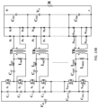
- FIG. 5 A illustrates a stacked half bridge resonant converter 500 , in accordance with an embodiment of the present disclosure.
- FIG. 5 B illustrates the timing diagrams for converter 500 in FIG. 5 A under variable frequency control for switch control signals GS 1 to GS 6 , resonant tank input voltages V AB V CD , and V EF , resonant capacitor voltages V cr1 , V cr2 , and V cr3 , and resonant currents i r2 , and i r3 , in accordance with an embodiment of the present disclosure.
- FIG. 5 C illustrates the timing diagrams for converter 500 in FIG.
- the DC-DC converter 500 includes a primary side, a secondary side, a control circuitry, a transformer stage electrically connected to the primary side and the secondary side, and at least one resonant tank circuit electrically connected between the primary side and the at least one transformer TR.
- the primary side includes a serial stack of at least two half-bridge inverter cells 501 , 502 , and 503 .
- the inverter cells 501 includes two active switches S 1 and S 2 in series in one leg and two input capacitors C 1 and C 2 in series in a parallel leg.
- the inverter cells 502 includes two active switches S 3 and S 4 in series in one leg and two input capacitors C 3 and C 4 in series in a parallel leg.
- the inverter cells 503 includes two active switches S 5 and S 6 in series in one leg and two input capacitors C 5 and C 6 in series in a parallel leg.
- the transformer stage includes a first transformer TR 1 , a second transformer TR 2 , and a third transformer TR 3
- the at least one resonant tank circuit includes a first resonant tank circuit, a second resonant tank circuit, and a third resonant tank circuit.
- each of the transformers TR 1 , TR 2 , and TR 3 includes a transformer core, a primary side winding wound on the transformer core, and a secondary side winding wound on the transformer core.
- the control circuitry is configured to activate the active switches S 1 , S 2 , S 3 , S 4 , S 5 , and S 6 to vary the pulse frequency or width or phase shift angle of voltage or current through the inverter cells or the rectifier circuit elements.
- rectifier rectifier circuit element
- rectifier cell rectifier cell
- Converter 500 employs three half bridges 501 , 502 , and 503 in stack on the primary side including switches S 1 to S 6 and also includes six input capacitors C 1 , C 2 , C 3 , C 4 , C 5 , and C 6 in stack.
- first half bridge 501 includes switches S 1 and S 2 connected in series and input capacitors C 1 and C 2 connected in series. Switches S 1 and S 2 and input capacitors C 2 and C 1 are connected together in series to form a first circuit loop.
- Point A between switches S 1 and S 2 is connected to one end of a first resonant tank including a resonant capacitor C r1 and a resonant inductor L r1 .
- the other end of the first resonant tank is connected to one end of the primary side winding of transformer TR 1 .
- the other end of the primary side winding of transformer TR 1 is connected to point B between input capacitors C 1 and C 2 .
- second half bridge 502 includes switches S 3 and S 4 connected in series and input capacitors C 3 and C 4 connected in series. Switches S 3 and S 4 and input capacitors C 4 and C 3 are connected together in series to form a second circuit loop.
- Point C between switches S 3 and S 4 is connected to one end of a second resonant tank including a resonant capacitor C r2 and a resonant inductor L r2 .
- the other end of the second resonant tank is connected to one end of the primary side winding of transformer TR 2 .
- the other end of the primary side winding of transformer TR 2 is connected to point D between input capacitors C 3 and C 4 . It is appreciated that the first and second circuit loops are directly connected.
- third half bridge 503 includes switches S 5 and S 6 connected in series and input capacitors C 5 and C 6 connected in series. Switches S 5 and S 6 and input capacitors C 6 and C 5 are connected together in series to form a third circuit loop.
- Point E between switches S 5 and S 6 is connected to one end of a third resonant tank including a resonant capacitor C r3 and a resonant inductor L r3 .
- the other end of the second resonant tank is connected to one end of the primary side winding of transformer TR 3 .
- the other end of the primary side winding of transformer TR 3 is connected to point F between input capacitors C 5 and C 6 . It is appreciated that the second and third circuit loops are directly connected, but the first and third circuit loops are not directly connected.
- each transformer's primary side winding is connected to a resonant tank which in turn is connected to the middle point of the corresponding switches, while the other end of each transformer's primary side winding is coupled to the middle point of the corresponding input capacitors.
- first terminal (between switch S 1 and input capacitor C 1 ) of first half bridge 501 is connected to a positive electrode of input voltage V in and a second terminal (between switch S 2 and input capacitor C 2 ) of first half bridge 501 is connected to a first terminal (between switch S 3 and input capacitor C 3 ) of second half bridge 502 .
- a second terminal (between switch S 4 and input capacitor C 4 ) of second half bridge 502 is connected to a first terminal (between switch S 5 and input capacitor C 5 ) of third half bridge 503 .
- a second terminal (between switch S 6 and input capacitor C 6 ) of third half bridge 503 is connected to a negative electrode of input voltage V in .
- first, second, and third half bridges 501 , 502 , 503 are “stacked” vertically to form a stacked half bridge.
- the secondary side includes at least two sets of rectifier circuit elements each coupled to a secondary side winding wound on the transformer core shared with a corresponding primary side winding and is configured to rectify current induced at the secondary side by current flowing in the corresponding primary side winding, and wherein a secondary side voltage V o is produced or applied.
- conventional three phase diode bridges including diodes D 1 , D 2 , D 3 , D 4 , D 5 , and D 6 ) are used in secondary side to provide rectification function.
- FIG. 5 B illustrates the timing diagrams for converter 500 in FIG. 5 A under variable frequency control for switch control signals GS 1 to GS 6 , resonant tank input voltages V AB V CD , and V EF , resonant capacitor voltages V cr1 , V cr2 , and V cr3 , and resonant currents i r1 , i r2 , and i r3 , in accordance with an embodiment of the present disclosure.
- Switch control signals GS 1 to GS 6 are the respective control signals of switches S 1 to S 6 .
- variable switching frequency control is used to regulate the output voltage and output power of stacked half bridge resonant converter 500 .
- all switches operate with the same switching frequency (e.g., 100 kHz or greater than 20 kHz) and have identical duty cycles of approximately 50%.
- the switch control signals of each half bridge are interleaved with each other with a phase shift of 120°.
- switch control signals GS 1 and GS 2 are phase shifted with respect to switch control signals GS 3 and GS 4 by 120 degrees.
- the resonant tank input voltages V AB , V CD and V EF are in a square waveform with no DC bias voltage.
- resonant capacitor voltages V cr1 , V cr2 , and V cr3 are in a sinusoidal waveform with no DC bias voltage.
- Resonant currents i r1 , i r2 , and i r3 for all three resonant tanks are pure sinusoid, if the resonant converter operates at its resonant frequency and the magnetizing current is negligible.
- Each resonant current is interleaved with each other with a phase shift of 120° due to the interleaved switch control signals. The interleaved currents can provide minimal ripple on the components to further improve the converter performance.
- Pulse Width Modulation for Stacked Half Bridge Resonant Converter
- Pulse width modulation (PWM) or variable duty cycle control is proposed to regulate the gain of the resonant circuit in this situation, when switching frequency control reaches its upper limit.
- FIG. 5 C illustrates the timing diagrams for converter 500 in FIG. 5 A under variable duty cycle control for switch control signals GS 1 to GS 6 , resonant capacitor voltages V cr1 to V cr3 , and resonant currents i r1 to i r3 , in accordance with an embodiment of the present disclosure.
- Switch control signals GS 1 to GS 6 are the respective control signals of switches S 1 to S 6 .
- the switch control signals of each half bridge are interleaved with each other with a phase shift of 120°.
- switch control signals GS 1 and GS 2 in the first leg are phase shifted with switch control signals GS 3 and GS 4 in the second leg by a phase shift angle of 120°.
- the duty cycle for switch control signals GS 1 to GS 6 are reduced from the nominal 50% to 40%, so as to further reduce the output voltage.
- the resonant currents i r1 to i r3 may become discontinuous in this modulation.
- FIG. 6 A illustrates a stacked half bridge LLC resonant converter 600 with active switches S 7 to S 12 on the secondary side for bidirectional operation, in accordance with an embodiment of the present disclosure.
- Converter 600 in FIG. 6 A is substantially identical to converter 500 in FIG. 5 A on the primary side. However, instead of diodes, converter 600 in FIG. 6 A employs three active half bridges in parallel on the secondary side including switches S 7 to S 12 for bidirectional operation.
- FIG. 6 B illustrates the timing diagrams for converter 600 in FIG. 6 A under variable frequency control and phase shift control for switch control signals GS 1 to GS 12 , resonant capacitor voltages V cr1 to V cr3 , and resonant currents i r1 to i r3 , in accordance with an embodiment of the present disclosure.
- Switch control signals GS 1 to GS 12 are the control signals of switches S 1 to S 12 .
- Variable switching frequency control is normally used to regulate the output voltage and output power in resonant converter. If wide input and/or output voltage range is required in specific applications, such as battery charging applications, implementing only the variable switching frequency control may not be able to achieve the required gain range.
- Phase shift modulation can be used to achieve wide input and/or output voltage range as well as bidirectional operation. As shown in FIG. 6 B , all switches operate with the same switching frequency and have identical duty cycles of approximately 50%. To achieve zero-voltage-switching of the complementary-operated primary side switches of the same leg, a small dead time is provided between the turn-on and turn-off instants of these complementary-operated switches.
- the switch control signals of each half bridge are interleaved with each other with a phase shift of about 120°.
- the switch control signals of each half bridge are also interleaved with each other with a phase shift of about 120°.
- the control signals of the first bridge on the primary side may be phase shifted with the control signals of the first bridge on the secondary side.
- Such a phase shift angle becomes another critical control variable besides the switching frequency.
- the output voltage and power are controlled by both the switching frequency and the phase shift angle.
- resonant capacitor voltages V cr1 to V cr3 have no DC-bias voltage due to the primary side circuit structure.
- Resonant currents i r1 to i r3 are interleaved with each other for 120° due to the interleaved switch control signals. These interleaved currents can provide minimal ripple on the components to further improve the converter performance.
- FIG. 7 A illustrates an n-stacked half bridge resonant converter 700 , in accordance with an embodiment of the present disclosure.
- Converter 700 employs n “stacked” half bridges on the primary side, including 2n switches S 1 to S (2n) and 2n input capacitors C 1 to C (2n) , where n is a natural number corresponding to the number of phases or resonant tanks in converter 700 .
- the middle point of each half bridge is connected to a resonant tank which includes a resonant capacitor and a resonant inductor.
- a total of n separated transformers may be used, and each transformer has a primary side winding and a secondary side winding.
- each transformer's primary side winding is connected to its corresponding middle point of the input capacitors and the second end of each transformer's primary side winding is connected to the other end of each resonant tank.
- a total of n half-wave diode bridges in parallel perform the secondary side rectification.
- Variable switching frequency control can be used to regulate the output voltage and output power of resonant converter 700 .
- All switches S 1 to S (2n) operate with the same switching frequency and have identical duty cycles of approximately 50%.
- the switch control signals of each half bridge are interleaved with each other with a phase shift of 360°/n, where n stands for the number of phases in converter 700 .
- the resonant currents for all resonant tanks are sinusoid if the magnetizing current is negligible when resonant converter 700 operates at its resonant frequency.
- Each resonant current is interleaved with each other with 360°/n phase shift angle due to the interleaved switch control signals. This interleaved current can provide the minimal ripple on the components to further improve the converter performance.
- the total n number of the separated transformer can be integrated to less than n number of transformers.
- FIG. 7 B shows an n-stacked half bridge resonant converter 700 that employs only one integrated transformer, which has total n windings on the primary side and n windings on the secondary side.
- FIG. 7 C illustrates an n-stacked half bridge resonant converter 700 with active switches on the secondary side for synchronous rectification and bidirectional operation.
- the 2n diodes on the secondary side as shown in FIGS. 7 A and 7 B are replaced by 2n active switches S O1 to S O(2n) for synchronous rectification to improve the operation efficiency.
- the resonant converter can also provide bidirectional power flow with the active switches.
- FIG. 8 A illustrates a three-stacked serial half bridge resonant converter 800 with a three-phase diode bridge rectifier, in accordance with an embodiment of the present disclosure.
- resonant converter 800 employs three serial half bridge inverter cells 801 , 802 , and 803 in stack, where each serial half bridge includes two half bridges (an upper half bridge and a lower half bridge) connected in series in a stacked structure.
- first serial half bridge inverter cell 801 includes four active switches S 1a , S 1b , S 1c and S 1d and two input capacitors C 1a and C 1b .
- Switches S 1a and S 1b which constitute an upper half bridge, are connected in parallel with input capacitor C 1a to form a circuit loop.
- Switches S 1 , and S 1d which constitute a lower half bridge, are connected in parallel with input capacitor C 1b to form another circuit loop.
- second serial half bridge inverter cell 802 includes four active switches S 2a , S 2b , S 2c and S 2d and two input capacitors C 2a and C 2b .
- Switches S 2a and S 2b which constitute an upper half bridge, are connected in parallel with input capacitor C 2a to form a circuit loop.
- Switches Sec and S 2d which constitute a lower half bridge, are connected in parallel with input capacitor C 2b to form another circuit loop.
- third serial half bridge inverter cell 803 includes four active switches S 3a , S 3b , S 3c , and S 3d and two input capacitors C 3a and C 3b .
- Switches S 3a and S 3b which constitute an upper half bridge, are connected in parallel with input capacitor C 3a to form a circuit loop.
- Switches S 2c and S 2d which constitute a lower half bridge, are connected in parallel with input capacitor C 2b to form another circuit loop.
- a middle point (point A) of the upper half bridges of first serial half bridge inverter cell 801 is connected to a resonant tank which includes a resonant capacitor C r1 and resonant inductor L r1 in series.
- a middle point (point C) of the upper half bridges of second serial half bridge inverter cell 802 is connected to a resonant tank which includes a resonant capacitor C r2 and resonant inductor L r2 in series.
- a middle point (point E) of the upper half bridges of third serial half bridge inverter cell 803 is connected to a resonant tank which includes a resonant capacitor C r3 and resonant inductor L r3 in series.
- each transformer has one primary side winding and one secondary side winding.
- a first end of each transformer's primary side winding is connected to a middle point (points B, D and F) of the lower half bridge of each serial-half-bridge.
- a second end of each transformer's primary side winding is coupled to the other side of each resonant tank.
- Three phase diode bridges 820 in parallel perform the secondary side rectification.
- Variable switching frequency control can be used to regulate the output voltage and output power of the stacked serial half bridge resonant converter 800 .
- FIG. 8 B illustrates the timing diagrams for the converter in FIG. 8 A under variable frequency control for switch control signals GS 1 to GS 6 , full bridge output voltages V AB to V EF , resonant capacitor voltage V cr1 to V cr3 , and resonant current i r1 to i r3 .
- all switches operate with the same switching frequency and have identical duty cycles of approximately 50%.
- a small dead time is provided between the turn-on and turn-off instants of these complementary-operated switches.
- the switch control signals of each serial half bridge are interleaved with each other with a phase shift angle of 120°.
- the peak-to-peak output voltage of each serial-half-bridge is 1 ⁇ 3 of the input voltage.
- the resonant capacitor voltages ⁇ Teri to vera have a DC bias voltage, which is equal to 1 ⁇ 6 of the input voltage.
- the resonant currents in three resonant tanks are sinusoid if the magnetizing current is negligible, when the resonant converter operates at its resonant frequency. Due to the interleaved switch control signals, the resonant currents are interleaved with each other with a phase shift angle of 120°. The interleaved currents provide the minimal ripple on the components to further improve the converter performance.
- FIG. 8 C illustrates a three-stacked serial half bridge resonant converter 800 with three full-wave diode bridges 830 in parallel for rectification, in accordance with an embodiment of the present disclosure.
- FIG. 8 B a total of three full-wave diode bridges are implemented on the secondary side in order to reduce the current stress of the secondary diodes in FIG. 8 A .
- the control signals of the primary side switches are the same as those shown in FIG. 8 B .
- FIG. 9 A illustrates an n-stacked serial half bridge resonant converter 900 with a total of n half-wave diode bridges in parallel for rectification, in accordance with an embodiment of the present disclosure.
- Resonant converter 900 employs n serial half bridges in stack, where each serial half bridge includes two half bridge in series.
- the (m)th serial half bridge has four active switches S ma , S mb , S mc and S md , together with two input capacitors C ma and C mb , where m can be any positive integer not larger than n.
- One of the two middle points of the (m)th serial half bridge is connected to a resonant tank which includes a resonant capacitor C rm and resonant inductor L rm in series.
- a resonant tank which includes a resonant capacitor C rm and resonant inductor L rm in series.
- a total of n separated transformers are used, and each transformer has one primary side winding and one secondary side winding.
- a first end of each transformer's primary side winding is connected to the other middle point of each serial half bridge and a second end of each transformer's primary side winding is connected to the other side of each resonant tank.
- a total of n half-wave diode bridges in parallel perform the secondary side rectification.
- Variable switching frequency control can be used to regulate the output voltage and output power of the stacked serial half bridge resonant converter 900 .
- All switches operate with the same switching frequency and have identical duty cycles of approximately 50%.
- a small dead time is provided between the turn-on and turn-off instants of these complementary-operated switches.
- the switch control signals of each serial half bridge are interleaved with each other with a phase shift of 360°/n.
- the four control signals of the first serial half bridge have 360°/n degree phase shift angle with the four control signals of the second serial half bridge.
- each resonant current is interleaved with each other with a phase shift angle of 360°/n.
- the interleaved currents provide the minimal ripple on the components to further improve the converter performance.
- FIG. 9 B illustrates an n-stacked serial half bridge resonant converter with an integrated transformer, in accordance with an embodiment of the present disclosure.
- FIG. 9 B can be replaced with active switches for synchronous rectification to improve the converter efficiency.
- Resonant converter 900 can provide bidirectional power flow with the active switches on both input and output sides.
- FIG. 9 C illustrates an n-stacked serial half bridge resonant converter with active switches on the secondary side for synchronous rectification and bidirectional operation, in accordance with an embodiment of the present disclosure. As shown in FIG. 9 C , the 2n diodes on the secondary side in FIG. 9 B are replaced with 2n active switches.
- FIG. 9 D illustrates an n-stacked serial half bridge resonant converter with total n full-wave diode bridges in parallel for rectification, in accordance with an embodiment of the present disclosure.
- a total of n full-wave diode bridges i.e., a total of 4n diodes
- the control signals of the primary side switches are the same as those in FIG. 9 A .
- the transformer integration and active switches on the secondary side can also be implemented in this structure.
- One challenge to operate a stacked half bridge resonant converter is to balance the input capacitor voltages when mismatches exist in the practical circuit, like capacitor equivalent series resistances (ESR) mismatch, timing mismatch of gate signals for the switches and the resonant parameters mismatch under practical tolerance.
- ESR capacitor equivalent series resistances
- FIG. 10 A illustrates a voltage balancing control diagram based on duty cycle method for the stacked half bridge resonant converter in FIG. 7 A , in accordance with an embodiment of the present disclosure.
- the voltages of the two capacitors for the (m)th half bridge cell are sensed as V Cma and V Cmb .
- Average values of the capacitor voltages of each half bridge cell is calculated and compared with a reference voltage V R . When the difference is greater than a predefined threshold voltage V th , a proper modified duty cycle is then generated by a dedicated controller and then implemented to balance the capacitor voltage.
- FIG. 10 B illustrates a voltage balancing control diagram based on duty cycle method for a stacked half bridge resonant converter with star connection of transformers, in accordance with an embodiment of the present disclosure.
- phase shift angle is adjusted between the control signals of each half bridge cell.
- 360°/n phase shift angle is implemented between the control signals of each half bridge cell.
- Vth a predefined threshold voltage
- a proper modified phase shift angle is then implemented to each phase leg to balance the capacitor voltage by changing the power delivered from each phase capacitor to the resonant tank.
- FIG. 10 C illustrates a voltage balancing control flow chart based on phase shift method for a three-stacked half bridge resonant converter, in accordance with an embodiment of the present disclosure.
- the voltages of a total of six input capacitors are sensed. Then, imbalance voltage for each phase ⁇ V A , ⁇ V B , and ⁇ V C , is calculated. If any of the imbalance voltage is greater than a threshold voltage Vth, proper modified phase shift angle is then implemented to each phase leg.
- FIG. 10 D illustrates a voltage balancing control flow chart based on phase shift method for a three-stacked half bridge resonant converter with star connection of transformers, in accordance with an embodiment of the present disclosure.
- the voltages of three input capacitors are sensed and imbalance voltage for each phase, ⁇ V A , ⁇ V B and ⁇ V C , is then calculated. If any of the imbalance voltage is greater than a threshold voltage V th , proper modified phase shift angle is then implemented to each phase leg.
- FIG. 10 E illustrates a voltage balancing control diagram based on a hybrid method for a stacked serial half bridge resonant converter, in accordance with an embodiment of the present disclosure.
- the first loop of the hybrid control scheme is the internal voltage balancing loop in each serial half bridge cell aiming to balance the two capacitor voltages inside each cell.
- the voltages of the two capacitors in each serial half bridge cell are sensed and compared with each other. If a voltage difference between these two capacitors is greater than a predefined threshold voltage Vth, a phase shift angle command is generated by a dedicated controller.
- each serial half bridge cell has its own internal phase shift angle between the switch signals of its first half bridge and its second half bridge, where the phase shift angle is calculated based on the voltage difference between its first input capacitor voltage and its second input capacitor voltage.
- the second loop of the control scheme is the external voltage balancing loop between all serial-half-bridge cells aiming to balance the average capacitor voltage of each cell.
- the voltages of the two capacitors in each serial-half-bridge cell are sensed and the average voltage of each cell is then calculated.
- the average voltage in then compared with the reference voltage. If the voltage difference is greater than the predefined threshold voltage, an extra duty cycle is generated by a dedicated controller.
- the extra duty cycle is implemented to all four switch control signals in a corresponding serial-half-bridge cell.
- each-serial-half bridge cell has its own extra duty cycle, where the extra duty cycle is calculated based on the voltage difference between its average capacitor voltage and the reference voltage. It is appreciated that the extra duty cycle can have a positive value or negative value with respect to the original duty cycle.
- FIG. 11 A illustrates a three stacked full bridge resonant converter 1100 , in accordance with an embodiment of the present disclosure.
- Converter 1100 employs three full bridge inverter cells 1101 , 1102 , and 1103 stacked together with three input capacitors C 1 to C 3 in series to block the DC input voltage.
- three separated transformers TR 1 , TR 2 , and TR 3 are used, and each transformer has one primary side winding and one secondary side winding.
- first full bridge inverter cell 1101 includes four switches S 1 , S 2 , S 3 , and S 4 .
- Point A between switches S 1 and S 3 is connected to one end of a resonant tank including a resonant capacitor C r1 and a resonant inductor L r1 in series.
- a first end of the primary side winding of transformer TR 1 is connected to the other side of the resonant tank.
- a second end of the primary side winding of transformer TR 1 is connected to point B between switches S 2 and S 4 .
- second full bridge inverter cell 1102 includes four switches S 5 , S 6 , S 7 , and S 8 .
- Point C between switches S 5 and S 7 is connected to one end of a resonant tank including a resonant capacitor C r2 and a resonant inductor L r2 in series.
- a first end of the primary side winding of transformer TR 2 is connected to the other side of the resonant tank.
- a second end of the primary side winding of transformer TR 2 is connected to point D between switches SG and S 8 .
- third full bridge inverter cell 1103 includes four switches S 9 , S 10 , S 11 , and S 12 .
- Point E between switches S 9 and S 11 is connected to one end of a resonant tank including a resonant capacitor C r3 and a resonant inductor L r3 in series.
- a first end of the primary side winding of transformer TR 3 is connected to the other side of the resonant tank.
- a second end of the primary side winding of transformer TR 3 is connected to point F between switches S 10 and S 12 .
- Three phase diode bridges 1120 in parallel perform the secondary side rectification, which is coupled with the secondary side windings of the three transformers TR 1 , TR 2 , and TR 3 .
- FIG. 11 B illustrates the timing diagrams for the converter in FIG. 11 A under variable frequency control for switch control signals GS 1 to GS 12 full bridge output voltage V AB to V EF , resonant capacitor voltage V cr1 to V cr3 , and resonant current i r1 to i r3 .
- all switches operate with the same switching frequency and have identical duty cycles of approximately 50%.
- a small dead time is provided between the turn-on and turn-off instants of these complementary-operated switches.
- the switch control signals of each full bridge are interleaved with each other full bridge control signals with a phase shift of 120°.
- GS 1 and GS 4 have 120° phase shift angle with respect to GS 5 and GS 8 .
- the resonant tank input voltage V AB , V CD , and V EF do not have a DC bias because each transformer is connected directly to the resonant tank.
- resonant capacitor voltages V cr1 , V cr2 , and V cr3 do not have a DC bias either.
- the resonant currents for all three resonant tanks are pure sinusoid if the resonant converter operates at its resonant frequency and the magnetizing current is negligible.
- Each resonant current is interleaved with each other for a phase shift of 120° due to the interleaved switch control signals. This interleaved current can provide the minimal ripple on the components to further improve the converter performance.
- FIG. 11 C illustrates an n-stacked full bridge resonant converter, in accordance with an embodiment of the present disclosure.
- the converter in FIG. 11 employs n full bridge inverter cells in stack together with n input capacitors C 1 to C n in series to block the DC input voltage.
- One of the two middle points of each full bridge is connected to a resonant tank which includes a resonant capacitor and resonant inductor in series.
- Total n separated transformers are used, and each transformer has one primary side winding and one secondary side winding. The first end of each transformer's primary side winding is connected to the other middle point of the full bridge and the second end of each transformer's primary side winding is connected to the other side of each resonant tank.
- Total n half-wave diode bridges in parallel perform the secondary side rectification.
- Variable switching frequency control can be used to regulate the output voltage and output power of n-stacked full bridge resonant converter. All switches operate with the same switching frequency and have identical duty cycles of approximately 50%. To achieve zero-voltage-switching of the complementary-operated primary side switches of the same leg, a small dead time is provided between the turn-on and turn-off instants of these complementary-operated switches.
- the switches control signals of each full bridge are interleaved with each other full bridge control signals with a phase shift of 360°/n.
- the resonant currents for all n resonant tanks are sinusoid if the magnetizing current is negligible when the resonant converter operates at its resonant frequency. Each resonant current is interleaved with each other with a phase shift of 360°/n due to the interleaved switch control signals.
- the interleaved currents provide the minimal ripple on the components to further improve the converter performance.
- FIG. 11 D illustrates an n-stacked full bridge resonant converter with a single integrated transformer, in accordance with an embodiment of the present disclosure.
- the single integrated transformer has total n windings on primary side and n windings on secondary side.
- FIG. 11 E illustrates an n-stacked full bridge resonant converter with active switches on the secondary side for synchronous rectification and bidirectional operation, in accordance with an embodiment of the present disclosure.
- 2n diodes are replaced with 2n active switches for synchronous rectification to improve the converter efficiency.
- the resonant converter is capable of providing bidirectional power flow with the active switches on both input and output side.
- FIG. 12 A illustrates a three stacked half bridge rectifier with transformer star connection applied in a three-phase resonant converter in accordance with an embodiment of the present disclosure.
- the three-phase resonant DC-DC converter includes a primary side, a secondary side, a transformer stage electrically coupled between the primary side and the secondary side, a control circuitry, and at least one resonant tank circuit electrically connected between the primary side and the transformer stage.
- the transformer stage includes a first transformer TR 1 , a second transformer TR 2 , and a third transformer TR 3
- the at least one resonant tank circuit includes a first resonant tank circuit, a second resonant tank circuit, and a third resonant tank circuit.
- each of the transformers TR 1 , TR 2 , and TR 3 includes a transformer core, a primary side winding wound on the transformer core, and a secondary side winding wound on the transformer core.
- the primary side includes a serial stack of at least two half-bridge inverter cells, each including two active switches S 1 and S 2 , S 3 and S 4 , or S 5 and S 6 in series in one leg and an input capacitor C 1 , C 2 or C 3 in a parallel leg together forming a first loop, wherein each inverter cell is connected from a point between the two active switches thereof through a corresponding resonant tank circuit to a first end of the primary side winding of the corresponding transformer, and through a second end of the primary side winding to a common star connection as point O of the corresponding ends of all the inverter cells, wherein one end of the first loop connecting the legs of one inverter cell is directly connected to the opposite end of the corresponding loop in an inverter cell on which said one inverter cell is stacked,
- the transformer cores of the transformers TR 1 , TR 2 , and TR 3 is integrated as one and shareable with the inverter cells.
- the secondary side includes at least two sets of rectifier circuit elements each coupled to the secondary side winding of the corresponding transformer shared with the corresponding primary side winding and is configured to rectify current induced at the secondary side by current flowing in the corresponding primary side winding, and wherein a secondary side voltage V o is produced or applied.
- This resonant rectifier employs three half bridges D 1 to D 6 in stack in the secondary side.
- First diode bridge D 1 and D 2 is connected in parallel with a first output capacitor C O1 .
- Second diode bridge D 3 and D 4 is connected in parallel with a second output capacitor C O2 .
- Third diode bridge D 5 and D 6 is connected in parallel with a third output capacitor C O3 .
- Output capacitors C O1 , C O2 , and C O3 are connected in series to provide the output voltage V O to a load R.
- the middle point of first diode bridge D 1 and D 2 is connected to one end of the secondary side winding of first transformer TR 2 through a DC-blocking capacitor C s1 .
- the middle point of second diode bridge D 3 and D 4 is connected to one end of the secondary side winding of second transformer TR 2 through a DC-blocking capacitor C s2 .
- the middle point of third diode bridge D 5 and D 6 is connected to one end of the secondary side winding of third transformer TR 3 through a DC-blocking capacitor C s3 .
- the other end of the secondary side winding of each transformer is connected together as point P, which is also defined as transformer star connection.
- the DC-blocking capacitors C s1 , C s2 , and C s3 establish the required DC bias voltage for the proper operation of the rectifier.
- FIG. 12 B illustrates the timing diagrams for the converter in FIG. 12 A under variable frequency control for switch control signals GS 1 to GS 6 , primary resonant current i r1 to i r3 , secondary current i s1 to i s3 , secondary blocking capacitor voltage V cs1 to V cs3 , output capacitor voltage V CO1 to V CO3 and output voltage V O .
- the transformer secondary current i s1 to i s3 are sinusoid in phase with the primary resonant current i r1 to i r3 .
- the blocking capacitor C s1 has a positive DC bias voltage
- the blocking capacitor C s3 has a negative DC bias voltage
- the blocking capacitor C s2 has an almost zero DC voltage.
- the three output capacitor voltages V CO1 to V CO3 are self-balanced as shown in FIG. 12 B .
- the output voltage is three times of each output capacitor voltage.
- FIG. 12 C illustrates an n-stacked half bridge rectifier with transformer star connection applied in an n-phase resonant converter, in accordance with an embodiment of the present disclosure.
- a total of n half bridge are stacked as the rectification stage of the n-stacked half bridge resonant converter.
- the output voltage is n times of each output capacitor voltage.
- FIG. 12 D illustrates an n-stacked half bridge rectifier with transformer star connection applied in an n-phase resonant converter with an integrated transformer, in accordance with an embodiment of the present disclosure. As shown in FIG. 12 D , only one integrated transformer is employed for an n-stacked half bridge rectifier.
- the integrated transformer has a total of n windings on the primary side and n windings on the secondary side.
- FIG. 12 E illustrates an n-stacked active half bridge rectifier with transformer star connection applied in an n-phase resonant converter for synchronous rectification and bidirectional operation, in accordance with an embodiment of the present disclosure.
- all diodes of the n-stacked half bridge rectifier are replaced with active switches for synchronous rectification.
- the resonant converter can provide bidirectional power flow.
- the phase shift modulation for stacked half bridge resonant converter can also be used in this topology.
- FIG. 13 A illustrates a three-stacked half bridge rectifier applied in a three-phase resonant converter, in accordance with an embodiment of the present disclosure.
- the resonant rectifier in FIG. 13 A employs three half bridges, D 1 through D 6 , in stack in the secondary side.
- First diode bridge D 1 and D 2 is connected in parallel with two output capacitors C O1 and C O2 .
- Second diode bridge D 3 and D 4 is connected in parallel with two output capacitors C O3 and C O4 .
- Third diode bridge D 5 and D 6 is connected in parallel with two output capacitors C O5 and C O6 .
- a total six output capacitors C O1 , C O2 , C O3 , C O4 , C O5 , and C O6 are connected in series to provide the output voltage V O to a load R.
- the middle point of first diode bridge D 1 and D 2 is connected to one end of the secondary side winding of first transformer TR 1 .
- the middle point of second diode bridge D 3 and D 4 is connected to one end of the secondary side winding of second transformer TR 2 .
- the middle point of third diode bridge D 5 and D 6 is connected to one end of the secondary side winding of third transformer TR 3 .
- the other end of the secondary side winding of first transformer TR 1 is connected to the middle point of output capacitors C O1 and C O2 .
- the other end of the secondary side winding of second transformer TR 2 is connected to the middle point of output capacitors C O3 and C O4 .
- the other end of the secondary side winding of third transformer TR 3 is connected to the middle point of output capacitors C O5 and C O6 .
- FIG. 13 B illustrates the timing diagrams for the converter in FIG. 13 A under variable frequency control for switch control signals GS 1 to GS 6 , primary resonant current i r1 to i r3 , secondary current i s1 to i s3 , output capacitor voltage V CO1 to V CO6 and output voltage V O .
- the transformer secondary current i s1 to i s3 are sinusoid in phase with the primary resonant current i r1 to i r3 .
- the six output capacitor voltages V CO1 to V CO6 are self-balanced as shown in FIG. 13 B .
- the output voltage is six times of each output capacitor voltage.
- FIG. 13 C illustrates an n-stacked half bridge rectifier applied in an n-phase resonant converter, in accordance with an embodiment of the present disclosure.
- a total of n number of half bridge are stacked as the rectification stage of the n-phase resonant converter.
- the output voltage is 2n times of each output capacitor voltage.
- FIG. 13 D illustrates an n-stacked half bridge rectifier applied in an n-phase resonant converter with an integrated transformer, in accordance with an embodiment of the present disclosure.
- FIG. 13 D only one integrated transformer for an n-stacked half bridge rectifier, which has a total of n windings on the primary side and n windings on the secondary side.
- FIG. 13 E illustrates an n-stacked active half bridge rectifier applied in an n-phase resonant converter for synchronous rectification and bidirectional operation, in accordance with an embodiment of the present disclosure.
- all diodes of the n-stacked half bridge rectifier are replaced with active switches for synchronous rectification.
- the resonant converter can provide bidirectional power flow.
- the phase shift modulation for stacked half bridge resonant converter can also be used in this topology.
- FIG. 14 A illustrates a three-stacked full bridge rectifier applied in a three-phase resonant converter, in accordance with an embodiment of the present disclosure.
- the resonant rectifier in FIG. 14 A employs three full bridges, including diodes D 1 through D 12 , in stack on the secondary side.
- First full bridge including diodes D 1 through D 4 is connected in parallel with first output capacitor C O1 .
- Second full bridge including diodes D 5 through D 8 is connected in parallel with second output capacitor C O2 .
- Third full bridge D 9 through D 12 is connected in parallel with third output capacitor C O3 .
- Output capacitors C O1 , C O2 , and C O3 are connected in series to provide output voltage V O to a load R.
- One end of the secondary side winding of first transformer TR 1 is connected to the middle point between diodes D 1 and D 3 , while the other end of the secondary side winding of first transformer TR 1 is connected to the middle point between diodes D 2 and D 4 .
- One end of the secondary side winding of second transformer TR 2 is connected to the middle point between diodes D 5 and D 7 , while the other end of the secondary side winding of second transformer TR 2 is connected to the middle point between diodes D 6 and D 8 .
- One end of the secondary side winding of third transformer TR 3 is connected to the middle point between diodes D 9 and D 11 , while the other end of the secondary side winding of third transformer TR 2 is connected to the middle point between diodes D 10 and D 12 .
- Variable switching frequency control can be applied to regulate the output voltage and output power of the stacked half bridge resonant converter with the proposed three-stacked full bridge rectifier. Blocking capacitors are not required in this rectifier.
- FIG. 14 B illustrates an n-stacked full bridge rectifier applied in an n-phase resonant converter, in accordance with an embodiment of the present disclosure.
- a total of n number of full bridges is stacked as the rectification stage of the n-stacked half bridge resonant converter.
- the output voltage is n times of each output capacitor voltage.
- FIG. 14 C illustrates an n-stacked full bridge rectifier applied in an n-phase resonant converter with an integrated transformer, in accordance with an embodiment of the present disclosure.
- an n-stacked full bridge rectifier employs only one integrated transformer, which has a total n windings on the primary side and n windings on the secondary side.
- FIG. 14 D illustrates an n-stacked active full bridge rectifier applied in an n-phase resonant converter for synchronous rectification and bidirectional operation, in accordance with an embodiment of the present disclosure.
- all diodes of the n-stacked full bridge rectifier are replaced with a total of 4n active switches for synchronous rectification.
- the resonant converter can provide bidirectional power flow.
- the phase shift modulation for stacked half bridge resonant converter can also be used in this topology.
- FIG. 15 A illustrates a three-stacked serial-half-bridge rectifier applied in a three-phase resonant converter, in accordance with an embodiment of the present disclosure.
- the resonant rectifier in FIG. 15 A employs three serial-half-bridges, including diodes D 1 through D 12 , in stack on the secondary side.
- First serial-half-bridge including diodes D 1 through D 4 is connected in parallel with two output capacitors C O1 and C O2 .
- Second serial-half-bridge including diodes D 5 through D 8 is connected in parallel with two output capacitors C O3 and C O4 .
- Third serial-half-bridge including diodes D 9 through D 12 is connected in parallel with two output capacitors C O5 and C O6 .
- a total of six output capacitors C O1 , C O2 , C O3 , C O4 , C O5 , and C O6 are connected in series to provide output voltage V O to a load R.
- One end of the secondary side winding of first transformer TR 1 is connected to the middle point between diodes D 1 and D 2 , while the other end of the secondary side winding of first transformer TR 1 is connected to the middle point between diodes D 3 and D 4 .
- One end of the secondary side winding of second transformer TR 2 is connected to the middle point between diodes D 5 and D 6 , while the other end of the secondary side winding of second transformer TR 2 is connected to the middle point between diodes D 7 and D 8 .
- One end of the secondary side winding of third transformer TR 3 is connected to the middle point between diodes D 9 and D 10 , while the other end of the secondary side winding of third transformer TR 3 is connected to the middle point between diodes D 11 and D 12 .
- Variable switching frequency control can be applied to regulate the output voltage and output power of the stacked half bridge resonant converter with the three-stacked serial-half-bridge rectifier of one embodiment of the present disclosure.
- the blocking capacitor C s1 to C s3 are applied to establish required DC bias voltage for the proper operation of the rectifier in FIG. 15 A .
- the six output capacitor voltages V CO1 to V CO6 are self-balanced.
- FIG. 15 B illustrates an n-stacked serial-half-bridge rectifier applied in an n-phase resonant converter, in accordance with an embodiment of the present disclosure.
- a total of n number of serial-half-bridges are stacked as the rectification stage of the n-stacked half bridge resonant converter.
- the output voltage is n times of each output capacitor voltage.
- FIG. 15 C illustrates an n-stacked serial-half-bridge rectifier applied in an n-phase resonant converter with an integrated transformer, in accordance with an embodiment of the present disclosure.
- an n-stacked serial-half-bridge rectifier employs only one integrated transformer, which has a total of n windings on the primary side and n windings on the secondary side.
- FIG. 15 D illustrates an n-stacked serial-half-bridge rectifier applied in an n-phase resonant converter for synchronous rectification and bidirectional operation, in accordance with an embodiment of the present disclosure.
- all diodes of the n-stacked serial-half-bridges rectifier are replaced with a total of 4n active switches for synchronous rectification.
- the resonant converter can provide bidirectional power flow.
- FIG. 16 illustrates a generalized stacked resonant converter, in accordance with an embodiment of the present disclosure.
- a total of n separated transformers is used with a total n primary side windings and n secondary side windings.
- On the primary side four different topologies can be used as the inverting stage. The first is the n-stacked half bridge structure with transformer star connection.
- the second is the n-stacked half bridge structure, which is the primary side of the topology in FIG. 7 A .
- the third topology is the n-stacked serial-half-bridge structure, which is the primary side of the topology in FIG. 9 A .
- the fourth topology is the n-stacked full bridge structure, which is the primary side of the topology in FIG. 11 C .
- the first is the n-stacked half bridge structure with transformer star connection, which is the rectifier of the topology in FIG. 12 C .
- secondary side blocking capacitors are required for proper operation of the rectifier.
- the second is the n-stacked half bridge structure, which is the rectifier of the topology in FIG. 13 C .
- the third topology is the n-stacked full bridge structure, which is the rectifier of the topology in FIG. 14 B .
- the fourth topology is the n-stacked serial-half-bridge structure, which is the rectifier of the topology in FIG. 15 B . In this situation, secondary side blocking capacitors are required for proper operation of the rectifier.
- the fifth rectifier is the conventional n-phase diode bridges structure, which can have a half-wave or a full-wave structure.
- N separated transformers are applied to provide required turns ratio and galvanic isolation.
- the n transformers can be further integrated into less than n transformers.
- the rectifier stage diodes can be replaced by active switches for synchronous rectification and bidirectional operation.
- Variable switching frequency control, PWM duty cycle modulation and phase shift modulation can be applied to regulate the output voltage and output power in this system.
- FIG. 17 illustrates a generalized stacked resonant converter including multiple circuits in parallel on both the primary and secondary sides, in accordance with an embodiment of the present disclosure.
- a total of m stacked structures is connected in parallel with the input voltage.
- Each stacked structure includes n stacked basic elements, which is the primary structure in FIG. 16 .
- m ⁇ n basic elements there is a total of m ⁇ n basic elements on the primary side with dedicated series and parallel connections.
- a total of m ⁇ n separated transformers, TR (1,1) to TR (n,m) are utilized with a total of m ⁇ n primary side windings and m ⁇ n secondary side windings.
- the basic stacking element is half bridge with transformer star connection, one end of every primary side winding is connected as a single point as star connection and the other end of every primary side winding is coupled to the middle point of every half bridge through the corresponding resonant tank. Otherwise, all the m ⁇ n primary side windings are directly coupled to the basic stacking elements through the resonant tanks.
- Each stacked structure includes q stacked basic circuit elements, which is similar to the rectifier stage in FIG. 16 .
- the product of p and q i.e., p ⁇ q
- m and n i.e., m ⁇ n.
- the basic stacking element is half bridge with transformer star connection, one end of every secondary side winding is connected at a single point as star connection and the other end of every secondary side winding is coupled to the middle point of every half bridge through a blocking capacitor. Otherwise, all the m ⁇ n secondary side windings are connected to the basic stacking elements through the blocking capacitors.
- Variable switching frequency control, PWM duty cycle modulation and phase shift modulation can be applied to regulate the output voltage and output power in this system.
- the m ⁇ n transformers can be integrated to less than m ⁇ n transformers for system simplicity.
- the rectifier stage diodes can be replaced by active switches for synchronous rectification and bidirectional operation.
Abstract
The present disclosure provides a series resonant converter and its corresponding control method. In one aspect, the series resonant converter includes m (m=1, 2, 3, . . . ) sets of primary side stages in parallel, wherein each primary side stage is identical and includes n (n=2, 3, . . . ) stacked element circuits, where the primary side stages receive an input voltage; n×m resonant networks coupled to the primary side stages; n×m transformers having n×m primary side windings and n×m secondary side windings, where the primary side windings are coupled to the n×m resonant networks; p (p=1, 2, 3, . . . ) sets of secondary side stages in parallel, wherein each secondary side stage is identical and includes q (q=n×m/p) stacked element circuits, where the secondary side stages are coupled to n×m secondary side windings; and a control block controlling the primary side switches according to the output voltage, input voltage and input capacitor voltages.
Description
This application claims the benefit of priority to U.S. Provisional Application No. 63/046,158, filed Jun. 30, 2020, the entire contents of which are incorporated herein by reference for all purposes.
This present disclosure relates to a DC-DC resonant converter and a control method thereof. More particularly, the present disclosure relates to a stacked-bridge resonant converter with switching frequency control and voltage balancing strategies.
The resonant converter, which employ a resonant-tank circuit to shape the switch voltage and/or current waveforms to minimize switching losses and allow high-frequency operation, has been widely employed as an isolated DC/DC converter, due to its high efficiency, simple structure achieved by magnetic integration, soft switching on both primary and secondary switches, and capability suitable for applications with wide voltage ranges.
For example, U.S. Pat. No. 6,344,979 to Huang et al, entitled “LLC Series Resonant DC-to-DC Converter”, issued Feb. 5, 2002, discloses an LLC resonant converter and its basic operation principles. FIGS. 1A and 1B respectively show a conventional full-bridge LLC resonant converter under closed-loop voltage control and the timing diagrams of control signals for switches S1 to S4 and a primary-side full-bridge output voltage VAB. Output voltage VAB may be regulated by controlling the switching frequency of these primary-side switches. Highest efficiency is attained when the LLC resonant converter operates at resonant frequency fr, determined by resonant inductor Lr and resonant capacitor Cr, and when DC voltage gain M equals the transformer's turns ratio NP/NS. DC voltage gain M diminishes when switching frequency fsw is greater than resonant frequency fr. Conversely, gain M becomes greater when switching frequency fsw is less than resonant frequency fr. Efficiency, however, always diminishes as switching frequency fsw moves away from resonant frequency fr. To achieve desired output voltage range, the LLC resonant converter should operate at its corresponding frequency range.
As shown in FIGS. 1A and 1B , the resonant tank includes inductor Lr and capacitors Cr connected in series, and the circuit can be referred to as a series-resonant converter. If the magnetizing inductance Lm of transformer TR is relatively small, i.e., if it is only several times of resonant inductance Lr, the converter can operate as an LLC series-resonant converter. It should be noted that the secondary-side diode rectifier (including diodes D1, D2, D3, and D4) can be implemented by a synchronous rectifier (e.g., using low on-resistance MOSFETs) to improve the efficiency. This implementation also makes the converter bidirectional, because controllable switches on both sides of the transformer allow power to flow in both directions. It should also be noted that the secondary-side of the isolated resonant converter can be implemented with a center-tapped secondary side winding instead of employing a full-wave rectifier as shown in FIG. 1A .
Generally, resonant converters are controlled by variable switching-frequency control. During above-resonant-frequency operations, the resonant converters operate with zero-voltage-switching (ZVS) of the primary switches, while during below-resonant-frequency operations, the resonant converters operate with zero-current switching (ZCS). More details about resonant converter topologies and control thereof can be found in Ref. [1].
Typical timing diagrams of switch-control signals for the series-resonant converter in FIG. 1A operating with ZVS are shown in FIG. 1B . As shown in FIG. 1B , all switches S1, S2, S3, and S4 operate with the same duty ratio of 50%. The primary side switches in the same leg (i.e., switches S1 and S2 in leg A and switches S3 and S4 in leg B) operate in a complementary fashion to avoid cross-conduction. The frequency of the primary side switches is determined by a feedback control loop that is employed to regulate the output. To achieve ZVS in practical implementations, the duty ratios of the primary switches are set to a value slightly less than 50% by introducing a short delay (or dead time) between the turn-off and the turn on of the complementary operated same-leg switches. During this dead time, the current is commutated from the switch of the device that is being turned off to the antiparallel diode of the other device which creates a condition for its subsequent ZVS turn on.
The full bridge structure is normally used in less than 800V DC input voltage applications when 1.2 kV devices are applied. In high input voltage applications, three-level topology in Ref. [2] is more attractive, because of the fact that each switching device needs to block only one half of the input voltage. Three-level topology is applied to LLC converters in Ref [3], in which the proposed converters achieve ZVS for the switches without additional auxiliary circuit. In Ref. [4], a three-level serial half bridge (SHB) topology, also known as stacked buck topology, is proposed for the first time. This topology removes the two clamping diodes in comparison with the conventional three-level topology from Ref. [2].
Generally, the power of a full bridge resonant converter based on a discrete device is limited to a few kilowatts because of the device's power rating. A three-phase LLC resonant converter is proposed in Ref. [5] to further increase the converter power by adding another half bridge phase leg in parallel to the existing legs on the primary side and another half bridge phase leg in parallel to the existing legs on the secondary side. The three-phase converter can have either three separated transformers or a single integrated transformer. The topology of a typical three phase LLC converter and its timing diagrams of switch-control are shown in FIGS. 3A and 3B . The switch-control signals of each primary half bridge are usually interleaved with each other with a 120-degree phase shift. This implementation can reduce the current and voltage ripple, thus reducing the stress on the components.
Recently, high input voltage (>2 kV) power supplies are more and more attractive in high power applications, such as a solid-stage-transformer, because they can deliver more power for the same amount of input current. A multi-phase multi-level LLC resonant converter with a star connection of transformers is proposed in Ref. [6] to satisfy the requirement for high-voltage and high-power applications. The topology of a multi-phase multi-level LLC resonant converter with three modules and its timing diagrams of switch-control shown in FIGS. 4A and 4B . The switch-control signals of each primary side half bridge are usually interleaved with each other with a 120-degree phase shift. However, the resonant capacitors in each phase leg suffer DC voltage bias due to the stacking structure and the star connection of the transformers. The bias voltage further increases when the input voltage increases. In addition, the voltage imbalance issue of the stacked capacitors and the bidirectional operation are not addressed in Ref. [6]. Therefore, there is a need to develop a DC/DC bidirectional resonant converter that is capable of operating in high input voltage and high-power applications, as well as reserving the merit of conventional resonant converters. There is also a need to develop a voltage balancing control strategy applied in multi-phase multi-level LLC resonant converters.
- [1] B. Yang, F. C. Lee, A. J. Zhang and G. Huang, “LLC resonant converter for front end DC/DC conversion,” APEC. Seventeenth Annual IEEE Applied Power Electronics Conference and Exposition (Cat. No. 02CH37335), Dallas, Tex., USA, 2002.
- [2] J. R. Pinheiro and I. Barbi, “The three-level ZVS PWM converter—a new concept in high voltage DC-to-DC conversion,” Proceedings of the 1992 International Conference on Industrial Electronics, Control, Instrumentation, and Automation, 1992.
- [3] Y. Gu, Z. Lu, L. Hang, Z. Qian and G. Huang, “Three-level LLC series resonant DC/DC converter,” IEEE Transactions on Power Electronics, vol. 20, no. 4, pp. 781-789, July 2005.
- [4] I. Barbi, R. Gules, R. Redl and N. O. Sokal, “DC-DC converter: four switches V/sub pk/=V/sub in//2, capacitive turn-off snubbing, ZV turn-on,” IEEE Transactions on Power Electronics, vol. 19, no. 4, pp. 918-927, July 2004.
- [5] T. Jin and K. Smedley, “Multiphase LLC Series Resonant Converter for Microprocessor Voltage Regulation,” Conference Record of the 2006 IEEE Industry Applications Conference Forty-First IAS Annual Meeting, Tampa, Fla., 2006, pp. 2136-2143.
- [6] F. Jin, F. Liu, X. Ruan and X. Meng, “Multi-phase multi-level LLC resonant converter with low voltage stress on the primary-side switches,” 2014 IEEE Energy Conversion Congress and Exposition (ECCE), Pittsburgh, Pa., 2014, pp. 4704-4710.
In one embodiment of the present disclosure, a DC-DC resonant converter with improved performance is disclosed. Specifically, the resonant converter of the embodiment of the present disclosure can be used in high power and high voltage applications by stacking a plurality of circuit elements in series.
In one aspect, one embodiment of the present disclosure provides a DC-DC converter including: a primary side including a serial stack of at least two half-bridge inverter cells, each including two active switches in series in one leg and two input capacitors in series in a parallel leg together forming a loop wherein each inverter cell is connected from a point between the switches to a resonant tank circuit to a primary side winding wound on a transformer core, and to a point between the two capacitors, wherein one end of the loop connecting the legs of one inverter cell is directly connected to the opposite end of the corresponding loop in an inverter cell on which it is stacked and a primary side voltage is applied or produced between the two ends of the loops of the serial stack of inverter cells that are not directly connected to another inverter cell and wherein the transformer core is sharable with other inverter cells; a secondary side including at least two sets of rectifier circuit elements each coupled to a secondary side winding wound on a transformer core shared with a corresponding primary side winding and is configured to rectify current induced at the secondary stage by current flowing in the corresponding primary side winding, and wherein a secondary side voltage is produced or applied; and control circuitry that activates switches in the converter to vary the pulse frequency or width or phase shift angle of voltage or current through inverter cells or rectifier circuits.
In one embodiment, the rectifier circuit elements are each a half-bridge rectifier cell including in a leg two diodes in series and oriented in the same direction between which is a connection to the corresponding secondary side winding to a common star connection of the corresponding ends of all the rectifiers, wherein corresponding ends of the diode legs form common connections with a parallel capacitor legs such that the secondary side voltage is produced between the two ends of the parallel legs.
In one embodiment, the rectifier circuit elements are each an active half-bridge rectifier including in a leg two active switches in series, each controlled by the control circuitry, between which switches is a connection to the corresponding secondary side winding to a common star connection of the corresponding ends of all the rectifier cells, wherein corresponding ends of the switch legs form common connections with a parallel capacitor leg such that the secondary side voltage is produced or applied between the two ends of the parallel legs.
In one embodiment, the rectifier circuit elements are each a full-bridge rectifier cell including two parallel legs of two diodes in series oriented in the same direction wherein each rectifier cell is connected from a point between the diodes of one leg to one end of the corresponding secondary side winding wound on the transformer core and through the other end of the winding to a point between the diodes of the other leg, wherein corresponding ends of the diode legs form common connections with a parallel capacitor leg such that the secondary side voltage is produced between the two ends of the parallel legs.
In one embodiment, the rectifier circuit elements are each a full-bridge rectifier cell including two parallel legs of two active switches in series, each controlled by the control circuitry, between which switches in a leg is a connection to one end of the corresponding secondary side winding wound on the transformer core and through the other end of the winding to a point between the switches of the other leg, wherein corresponding ends of the switch legs form common connections with a parallel capacitor leg such that the secondary side voltage is produced or applied between the two ends of the parallel legs.
In one embodiment, the rectifier circuit elements form a serial stack of half-bridge rectifier cells, each including two diodes in series oriented in the same direction in one leg and two capacitors in series in a parallel leg together forming a loop wherein each rectifier cell is connected from a point between the diodes to one end of the corresponding secondary side winding wound on the transformer core and through the other end of the winding to a point between the two capacitors, wherein one end of the loop connecting the parallel legs of one rectifier cell is directly connected to the opposite end of the corresponding loop in a rectifier cell on which it is stacked and a secondary side voltage is produced between the two ends of the loops of the serial stack of rectifier cells that are not directly connected to another rectifier cell.
In one embodiment, the rectifier circuit elements form a serial stack of half-bridge rectifier cells, each including two active switches in series in one leg, each controlled by the control circuitry, and two capacitors in series in a parallel leg together forming a loop wherein each rectifier cell is connected from a point between the switches to one end of the corresponding secondary side winding wound on the transformer core and through the other end of the winding to a point between the two capacitors, wherein one end of the loop connecting the parallel legs of one rectifier cell is directly connected to the opposite end of the corresponding loop in a rectifier cell on which it is stacked and a secondary side voltage is produced or applied between the two ends of the loops of the serial stack of rectifier cells that are not directly connected to another rectifier cell.
In one embodiment, the rectifier circuit elements form a serial stack of half-bridge rectifier cells, each including two diodes in series oriented in the same direction in one leg and a capacitor in a parallel leg together forming a loop wherein each rectifier cell is connected from a point between the diodes through a blocking capacitor to one end of the corresponding secondary side winding wound on the transformer core and through the other end of the winding to a common star connection of the corresponding ends of all the rectifier cells, wherein one end of the loop connecting the parallel legs of one rectifier cell is directly connected to the opposite end of the corresponding loop in a rectifier cell on which it is stacked and a secondary side voltage is produced between the two ends of the loops of the serial stack of rectifier cells that are not directly connected to another rectifier cell.
In one embodiment, the rectifier circuit elements form a serial stack of half-bridge rectifier cells, each including two active switches in series in one leg, each controlled by the control circuitry, and a capacitors in a parallel leg together forming a loop wherein each rectifier cell is connected from a point between the switches through a blocking capacitor to one end of the corresponding secondary side winding wound on the transformer core and through the other end of the winding to a common star connection of the corresponding ends of all the rectifier cells, wherein one end of the loop connecting the parallel legs of one rectifier cell is directly connected to the opposite end of the corresponding loop in a rectifier cell on which it is stacked and a secondary side voltage is produced or applied between the two ends of the loops of the serial stack of rectifier cells that are not directly connected to another rectifier cell.
In one embodiment, the rectifier circuit elements form a serial stack of full-bridge rectifier cells, each including two legs of two diodes in series oriented in the same direction and a capacitor leg in parallel connected at each end of the respective legs wherein each rectifier cell is connected from a point between the diodes of one leg to one end of the corresponding secondary side winding wound on the transformer core and through the other end of the winding to a point between the diodes of the other leg, wherein one connection of the parallel legs of one rectifier cell is directly connected to the opposite side connection of the parallel legs of a rectifier cell on which it is stacked and a secondary side voltage is produced or applied between the two connections of parallel legs of the serial stack of rectifier cells that are not directly connected to another rectifier cell.
In one embodiment, the rectifier circuit elements form a serial stack of full-bridge rectifier cells, each including two legs of two active switches in series, each controlled by the control circuitry, and a capacitor leg in parallel connected at each end of the respective legs wherein each rectifier cell is connected from a point between the switches of one leg to one end of the corresponding secondary side winding wound on the transformer core and through the other end of the winding to a point between the switches of the other leg, wherein one connection of the parallel legs of one rectifier cell is directly connected to the opposite side connection of the parallel legs of a rectifier cell on which it is stacked and a secondary side voltage is produced or applied between the two connections of parallel legs of the serial stack of rectifier cells that are not directly connected to another rectifier cell.
In one embodiment, the rectifier circuit elements form a serial stack of serial-half-bridge rectifier cells, each including a first set of two diodes oriented in the same direction in a first series leg and a capacitor in a parallel leg connected at each end of the legs to form a first loop connecting at its reverse end to the forward end of a second loop of two diodes oriented in the same direction in a second series leg and a capacitor in a parallel leg, wherein each rectifier cell is connected from a point between the diodes of the first series leg through a blocking capacitor to one end of the corresponding secondary side winding wound on the transformer core and through the other end of the winding to a point between the diodes of the second series leg, wherein the reverse end of the stacked loops of one rectifier cell is directly connected to the forward end of the stacked loops of a rectifier cell on which it is stacked and a secondary side voltage is produced between the two ends of the loops of the serial stack of rectifier cells that are not directly connected to another loop.
In one embodiment, the rectifier circuit elements form a serial stack of serial-half-bridge rectifier cells, each including a first set of two active switches, each controlled by the control circuitry, in a first series leg and a capacitor in a parallel leg connected at each end of the legs to form a first loop connecting at a reverse end to a forward end of a second loop of two active switches, each controlled by the control circuitry, in a second series leg and a capacitor in a parallel leg, wherein each rectifier cell is connected from a point between the switches of the first series leg through a blocking capacitor to one end of the corresponding secondary side winding wound on the transformer core and through the other end of the winding to a point between the switches of the second series leg, wherein the reverse end of the stacked loops of one rectifier cell is directly connected to the forward end of the stacked loops of a rectifier cell on which it is stacked and a secondary side voltage is produced or applied between the two ends of the loops of the serial stack of rectifier cells that are not directly connected to another loop.
In one embodiment, the control circuitry determines whether the average of voltages detected across the two input capacitors of an inverter cell is greater than a reference voltage and, if so, adjusts the inverter cell duty cycles through the two switches to balance the capacitor voltages.
In one embodiment, the control circuitry determines whether any of the average voltages across the two input capacitors of each inverter cell minus a reference voltage is greater than a threshold voltage and, if so, determines the greatest difference among the cells and adjusts the phase shift angle to each phase leg through the two switches to balance the capacitor voltages.
In another aspect, one embodiment of the present disclosure provides a DC-DC converter including: a primary side including sets of at least two serial half-bridge inverter cells, each including a first half-bridge of two active switches in a first series leg and an input capacitor in a parallel leg connected at each end of the legs to form a first loop connecting at a reverse end to a forward end of a second half-bridge loop of two active switches in a second series leg and a capacitor in a parallel leg, wherein each inverter cell is connected from a point between the switches of the first series leg through a resonant tank circuit, through the primary side winding wound on a transformer core to a point between the switches of the second series leg, wherein the reverse end of the stacked loops of one inverter cell is directly connected to the forward end of the stacked loops of an inverter cell on which it is stacked and a primary side voltage is applied or produced between the two ends of the loops of the serial stack of inverter cells that are not directly connected to another loop and wherein the transformer core is shared with other inverter cells; a secondary side including at least two sets of rectifier circuit elements each coupled to a secondary side winding wound on the transformer core shared with a corresponding primary side winding and is configured to rectify current induced at the secondary stage by current flowing in the corresponding primary side winding, and wherein a secondary side voltage is produced or applied; and control circuitry that activates switches in the converter to vary the pulse frequency or width or phase shift angle of voltage or current through inverter or rectifier circuits.
In one embodiment, the rectifier circuit elements are each a half-bridge rectifier including in a leg two diodes in series and oriented in the same direction between which is a connection to the corresponding secondary side winding to a common star connection of the corresponding ends of all the rectifier cells, wherein corresponding ends of the diode legs form common connections with a parallel capacitor legs such that the secondary side voltage is produced between the two ends of the parallel legs.
In one embodiment, the secondary circuit elements are each an active half-bridge rectifier cell including in a leg two active switches in series, each controlled by the control circuitry, between which switches is a connection to the corresponding secondary side winding to a common star connection of the corresponding ends of all the rectifier cells, wherein corresponding ends of the switch legs form common connections with a parallel capacitor leg such that the secondary side voltage is produced or applied between the two ends of the parallel legs.
In one embodiment, the rectifier circuit elements are each a full-bridge rectifier including two parallel legs of two diodes in series oriented in the same direction wherein each rectifier cell is connected from a point between the diodes of one leg to one end of the corresponding secondary side winding wound on the transformer core and through the other end of the winding to a point between the diodes of the other leg, wherein corresponding ends of the diode legs form common connections with a parallel capacitor leg such that the secondary side voltage is produced between the two ends of the parallel legs.
In one embodiment, the rectifier circuit elements are each a full-bridge rectifier including two parallel legs of two active switches in series, each controlled by the control circuitry, between which switches in a leg is a connection to one end of the corresponding secondary side winding wound on the transformer core and through the other end of the winding to a point between the switches of the other leg, wherein corresponding ends of the switch legs form common connections with a parallel capacitor leg such that the secondary side voltage is produced or applied between the two ends of the parallel legs.
In one embodiment, the rectifier circuit elements form a serial stack of half-bridge rectifier cells, each including two diodes in series oriented in the same direction in one leg and two capacitors in series in a parallel leg together forming a loop wherein each rectifier cell is connected from a point between the diodes to one end of the corresponding secondary side winding wound on the transformer core and through the other end of the winding to a point between the two capacitors, wherein one end of the loop connecting the parallel legs of one rectifier cell is directly connected to the opposite end of the corresponding loop in a rectifier cell on which it is stacked and a secondary side voltage is produced between the two ends of the loops of the serial stack of rectifier cells that are not directly connected to another rectifier cell.
In one embodiment, the rectifier circuit elements form a serial stack of half-bridge rectifier cells, each including two active switches in series in one leg, each controlled by the control circuitry, and two capacitors in series in a parallel leg together forming a loop wherein each rectifier cell is connected from a point between the switches to one end of the corresponding secondary side winding wound on the transformer core and through the other end of the winding to a point between the two capacitors, wherein one end of the loop connecting the parallel legs of one rectifier cell is directly connected to the opposite end of the corresponding loop in a rectifier cell on which it is stacked and a secondary side voltage is produced or applied between the two ends of the loops of the serial stack of rectifier cells that are not directly connected to another rectifier cell.
In one embodiment, the rectifier circuit elements form a serial stack of half-bridge rectifier cells, each including two diodes in series oriented in the same direction in one leg and a capacitor in a parallel leg together forming a loop wherein each rectifier cell is connected from a point between the diodes through a blocking capacitor to one end of the corresponding secondary side winding wound on the transformer core and through the other end of the winding to a common star connection of the corresponding ends of all the rectifier cells, wherein one end of the loop connecting the parallel legs of one rectifier cell is directly connected to the opposite end of the corresponding loop in a rectifier cell on which it is stacked and a secondary side voltage is produced between the two ends of the loops of the serial stack of rectifier cells that are not directly connected to another rectifier cell.
In one embodiment, the rectifier circuit elements form a serial stack of half-bridge rectifier cells, each including two active switches in series in one leg, each controlled by the control circuitry, and a capacitors in a parallel leg together forming a loop wherein each rectifier cell is connected from a point between the switches through a blocking capacitor to one end of the corresponding secondary side winding wound on the transformer core and through the other end of the winding to a common star connection of the corresponding ends of all the rectifier cells, wherein one end of the loop connecting the parallel legs of one rectifier cell is directly connected to the opposite end of the corresponding loop in a rectifier cell on which it is stacked and a secondary side voltage is produced or applied between the two ends of the loops of the serial stack of rectifier cells that are not directly connected to another rectifier cell.
In one embodiment, the rectifier circuit elements form a serial stack of full-bridge rectifier cells, each including two legs of two diodes in series oriented in the same direction and a capacitor leg in parallel connected at each end of the respective legs wherein each rectifier cell is connected from a point between the diodes of one leg to one end of the corresponding secondary side winding wound on the transformer core and through the other end of the winding to a point between the diodes of the other leg, wherein one connection of the parallel legs of one rectifier cell is directly connected to the opposite side connection of the parallel legs of a rectifier cell on which it is stacked and a secondary side voltage is produced or applied between the two connections of parallel legs of the serial stack of rectifier cells that are not directly connected to another rectifier cell.
In one embodiment, the rectifier circuit elements form a serial stack of full-bridge rectifier cells, each including two legs of two active switches in series, each controlled by the control circuitry, and a capacitor leg in parallel connected at each end of the respective legs wherein each rectifier cell is connected from a point between the switches of one leg to one end of the corresponding secondary side winding wound on the transformer core and through the other end of the winding to a point between the switches of the other leg, wherein one connection of the parallel legs of one rectifier cell is directly connected to the opposite side connection of the parallel legs of a rectifier cell on which it is stacked and a secondary side voltage is produced or applied between the two connections of parallel legs of the serial stack of rectifier cells that are not directly connected to another rectifier cell.
In one embodiment, the rectifier circuit elements form a serial stack of serial-half-bridge rectifier cells, each including a first set of two diodes oriented in the same direction in a first series leg and a capacitor in a parallel leg connected at each end of the legs to form a first loop connecting at its reverse end to the forward end of a second loop of two diodes oriented in the same direction in a second series leg and a capacitor in a parallel leg, wherein each rectifier cell is connected from a point between the diodes of the first series leg through a blocking capacitor to one end of the corresponding secondary side winding wound on the transformer core and through the other end of the winding to a point between the diodes of the second series leg, wherein the reverse end of the stacked loops of one rectifier cell is directly connected to the forward end of the stacked loops of a rectifier cell on which it is stacked and a secondary side voltage is produced between the two ends of the loops of the serial stack of rectifier cells that are not directly connected to another loop.
In one embodiment, the rectifier circuit elements form a serial stack of serial-half-bridge rectifier cells, each including a first set of two active switches, each controlled by the control circuitry, in a first series leg and a capacitor in a parallel leg connected at each end of the legs to form a first loop connecting at a reverse end to a forward end of a second loop of two active switches, each controlled by the control circuitry, in a second series leg and a capacitor in a parallel leg, wherein each rectifier cell is connected from a point between the switches of the first series leg through a blocking capacitor to one end of the corresponding secondary side winding wound on the transformer core and through the other end of the winding to a point between the switches of the second series leg, wherein the reverse end of the stacked loops of one rectifier cell is directly connected to the forward end of the stacked loops of a rectifier cell on which it is stacked and a secondary side voltage is produced or applied between the two ends of the loops of the serial stack of rectifier cells that are not directly connected to another loop.
In one embodiment, the control circuitry determines for each inverter cell whether a detected voltage difference across the two input capacitors is greater than a threshold voltage, and if so, adjusts the phase shift angle through the four switches in the corresponding cell; and determines for each inverter cell whether the average voltage across the two input capacitors is greater than a reference voltage, and if so, generates an extra duty cycle through the four switches in the corresponding cell.
The use of the word “a” or “an” when used in conjunction with the term “comprising/including” in the claims and/or the specification may mean “one,” but it is also consistent with the meaning of “one or more,” “at least one,” and “one or more than one.”
The use of the term “or” in the claims is used to mean “and/or” unless explicitly indicated to refer to alternatives only or the alternative are mutually exclusive, although the disclosure supports a definition that refers to only alternatives and “and/or.”
Other objects, features and advantages of the present invention will become apparent from the following detailed description. It should be understood, however, that the detailed description and the specific examples, while indicating specific embodiments of the invention, are given by way of illustration only, since various changes and modifications within the spirit and scope of the invention will become apparent to those skilled in the art from this detailed description.
The present disclosure is better understood upon consideration of the following detailed description and the accompanying drawings.
The present invention will now be described more specifically with reference to the following embodiments. It is to be noted that the following descriptions of preferred embodiments of this invention are presented herein for purpose of illustration and description only; it is not intended to be exhaustive or to be limited to the precise form disclosed. For example, the formation of a first feature over or on a second feature in the description that follows may include embodiments in which the first and second features are formed in direct contact, and may also include embodiments in which additional features may be formed between the first and second features, such that the first and second features may not be in direct contact. In addition, the present disclosure may repeat reference numerals and/or letters in the various examples. This repetition is for the purpose of simplicity and clarity and does not in itself dictate a relationship between the various embodiments and/or configurations discussed. Further, spatially relative terms, such as “beneath,” “below,” “lower,” “above,” “upper” and the like, may be used herein for ease of description to describe one element or feature's relationship to another element(s) or feature(s) as illustrated in the figures. The spatially relative terms are intended to encompass different orientations of the device in use or operation in addition to the orientation depicted in the figures. The apparatus may be otherwise oriented (rotated 90 degrees or at other orientations) and the spatially relative descriptors used herein may likewise be interpreted accordingly. When an element is referred to as being “connected,” or “coupled,” to another element, it can be directly connected or coupled to the other element or intervening elements may be present. Although the wide numerical ranges and parameters of the present disclosure are approximations, numerical values are set forth in the specific examples as precisely as possible. In addition, although the “first,” “second,” “third,” and the like terms in the claims be used to describe the various elements can be appreciated, these elements should not be limited by these terms, and these elements are described in the respective embodiments are used to express the different reference numerals, these terms are only used to distinguish one element from another element. For example, a first element could be termed a second element, and, similarly, a second element could be termed a first element, without departing from the scope of example embodiments. Besides, “and/or” and the like may be used herein for including any or all combinations of one or more of the associated listed items. While the numerical ranges and parameters set forth for the broad scope of the present invention are approximations, the numerical value reported in the specific examples set forth as accurately as possible. However, any numerical values inherently contain certain errors necessarily the standard deviation found in the respective testing measurements caused. Also, as used herein, the term “about” generally means away from a given value or a range of 10%, 5%, 1% or 0.5%. Alternatively, the word “about” means within an acceptable standard error of ordinary skill in the art-recognized average. In addition to the operation/working examples, or unless otherwise specifically stated otherwise, in all cases, all of the numerical ranges, amounts, values and percentages, such as the number for the herein disclosed materials, time duration, temperature, operating conditions, the ratio of the amount, and the like, should be understood as the word “about” decorator. Accordingly, unless otherwise indicated, the numerical parameters of the present invention and scope of the appended patent proposed is to follow changes in the desired approximations. At least, the number of significant digits for each numerical parameter should at least be reported and explained by conventional rounding technique is applied. Herein, it can be expressed as a range between from one endpoint to the other or both endpoints. Unless otherwise specified, all ranges disclosed herein are inclusive.
A. Stacked Half Bridge Resonant Converter
Three Stacked Half Bridge Resonant Converter
In the embodiment, the DC-DC converter 500 includes a primary side, a secondary side, a control circuitry, a transformer stage electrically connected to the primary side and the secondary side, and at least one resonant tank circuit electrically connected between the primary side and the at least one transformer TR. The primary side includes a serial stack of at least two half- bridge inverter cells 501, 502, and 503. The inverter cells 501 includes two active switches S1 and S2 in series in one leg and two input capacitors C1 and C2 in series in a parallel leg. The inverter cells 502 includes two active switches S3 and S4 in series in one leg and two input capacitors C3 and C4 in series in a parallel leg. The inverter cells 503 includes two active switches S5 and S6 in series in one leg and two input capacitors C5 and C6 in series in a parallel leg. In the embodiment, the transformer stage includes a first transformer TR1, a second transformer TR2, and a third transformer TR3, and the at least one resonant tank circuit includes a first resonant tank circuit, a second resonant tank circuit, and a third resonant tank circuit. In the embodiment, each of the transformers TR1, TR2, and TR3 includes a transformer core, a primary side winding wound on the transformer core, and a secondary side winding wound on the transformer core. The control circuitry is configured to activate the active switches S1, S2, S3, S4, S5, and S6 to vary the pulse frequency or width or phase shift angle of voltage or current through the inverter cells or the rectifier circuit elements.
It should be noted that the terms “rectifier,” “rectifier circuit element,” “rectifier cell,” and the like in the disclosure may mean the same in some embodiments and may be used herein for ease of description to describe one element or feature utilized for providing rectification function.
Likewise, as shown in FIG. 5A , second half bridge 502 includes switches S3 and S4 connected in series and input capacitors C3 and C4 connected in series. Switches S3 and S4 and input capacitors C4 and C3 are connected together in series to form a second circuit loop. Point C between switches S3 and S4 is connected to one end of a second resonant tank including a resonant capacitor Cr2 and a resonant inductor Lr2. The other end of the second resonant tank is connected to one end of the primary side winding of transformer TR2. The other end of the primary side winding of transformer TR2 is connected to point D between input capacitors C3 and C4. It is appreciated that the first and second circuit loops are directly connected.
Further, as shown in FIG. 5A , third half bridge 503 includes switches S5 and S6 connected in series and input capacitors C5 and C6 connected in series. Switches S5 and S6 and input capacitors C6 and C5 are connected together in series to form a third circuit loop. Point E between switches S5 and S6 is connected to one end of a third resonant tank including a resonant capacitor Cr3 and a resonant inductor Lr3. The other end of the second resonant tank is connected to one end of the primary side winding of transformer TR3. The other end of the primary side winding of transformer TR3 is connected to point F between input capacitors C5 and C6. It is appreciated that the second and third circuit loops are directly connected, but the first and third circuit loops are not directly connected.
In sum, in this embodiment, three separated transformers TR1, TR2, and TR3 are used where one end of each transformer's primary side winding is connected to a resonant tank which in turn is connected to the middle point of the corresponding switches, while the other end of each transformer's primary side winding is coupled to the middle point of the corresponding input capacitors.
In one embodiment, a first terminal (between switch S1 and input capacitor C1) of first half bridge 501 is connected to a positive electrode of input voltage Vin and a second terminal (between switch S2 and input capacitor C2) of first half bridge 501 is connected to a first terminal (between switch S3 and input capacitor C3) of second half bridge 502. A second terminal (between switch S4 and input capacitor C4) of second half bridge 502 is connected to a first terminal (between switch S5 and input capacitor C5) of third half bridge 503. A second terminal (between switch S6 and input capacitor C6) of third half bridge 503 is connected to a negative electrode of input voltage Vin. In other words, first, second, and third half bridges 501, 502, 503, each forming a circuit loop, are “stacked” vertically to form a stacked half bridge.
In one embodiment, the secondary side includes at least two sets of rectifier circuit elements each coupled to a secondary side winding wound on the transformer core shared with a corresponding primary side winding and is configured to rectify current induced at the secondary side by current flowing in the corresponding primary side winding, and wherein a secondary side voltage Vo is produced or applied. In the embodiment, conventional three phase diode bridges (including diodes D1, D2, D3, D4, D5, and D6) are used in secondary side to provide rectification function.
Variable Switching Frequency Control for Three Stacked Half Bridge Resonant Converter
As shown in FIG. 5B , all switches operate with the same switching frequency (e.g., 100 kHz or greater than 20 kHz) and have identical duty cycles of approximately 50%. To achieve zero-voltage-switching of the complementary-operated primary side switches of the same leg, a small dead time is provided between the turn-on and turn-off instants of these complementary-operated switches. The switch control signals of each half bridge are interleaved with each other with a phase shift of 120°. For example, switch control signals GS1 and GS2 are phase shifted with respect to switch control signals GS3 and GS4 by 120 degrees. In this embodiment, the resonant tank input voltages VAB, VCD and VEF are in a square waveform with no DC bias voltage. For the same reason, resonant capacitor voltages Vcr1, Vcr2, and Vcr3 are in a sinusoidal waveform with no DC bias voltage. Resonant currents ir1, ir2, and ir3 for all three resonant tanks are pure sinusoid, if the resonant converter operates at its resonant frequency and the magnetizing current is negligible. Each resonant current is interleaved with each other with a phase shift of 120° due to the interleaved switch control signals. The interleaved currents can provide minimal ripple on the components to further improve the converter performance.
Pulse Width Modulation (PWM) for Stacked Half Bridge Resonant Converter
If wide input and/or output voltage range is required in specific applications, such as in battery charging applications, implementing only the variable switching frequency control may not be able to achieve the required gain range. Pulse width modulation (PWM) or variable duty cycle control is proposed to regulate the gain of the resonant circuit in this situation, when switching frequency control reaches its upper limit.
Phase Shift Modulation for Stacked Half Bridge Resonant Converter
Variable switching frequency control is normally used to regulate the output voltage and output power in resonant converter. If wide input and/or output voltage range is required in specific applications, such as battery charging applications, implementing only the variable switching frequency control may not be able to achieve the required gain range. Phase shift modulation can be used to achieve wide input and/or output voltage range as well as bidirectional operation. As shown in FIG. 6B , all switches operate with the same switching frequency and have identical duty cycles of approximately 50%. To achieve zero-voltage-switching of the complementary-operated primary side switches of the same leg, a small dead time is provided between the turn-on and turn-off instants of these complementary-operated switches.
On the primary side, the switch control signals of each half bridge are interleaved with each other with a phase shift of about 120°. On the secondary side, the switch control signals of each half bridge are also interleaved with each other with a phase shift of about 120°. In addition, in one embodiment, the control signals of the first bridge on the primary side may be phase shifted with the control signals of the first bridge on the secondary side. Such a phase shift angle becomes another critical control variable besides the switching frequency. In other words, the output voltage and power are controlled by both the switching frequency and the phase shift angle. In this embodiment, resonant capacitor voltages Vcr1 to Vcr3 have no DC-bias voltage due to the primary side circuit structure. Resonant currents ir1 to ir3 are interleaved with each other for 120° due to the interleaved switch control signals. These interleaved currents can provide minimal ripple on the components to further improve the converter performance.
n-Stacked Half Bridge Resonant Converter
Variable switching frequency control can be used to regulate the output voltage and output power of resonant converter 700. All switches S1 to S(2n) operate with the same switching frequency and have identical duty cycles of approximately 50%. To achieve zero-voltage-switching of the complementary-operated primary side switches of the same half bridge, a small dead time is provided between the turn-on and turn-off instants of these complementary-operated switches. The switch control signals of each half bridge are interleaved with each other with a phase shift of 360°/n, where n stands for the number of phases in converter 700. The resonant currents for all resonant tanks are sinusoid if the magnetizing current is negligible when resonant converter 700 operates at its resonant frequency. Each resonant current is interleaved with each other with 360°/n phase shift angle due to the interleaved switch control signals. This interleaved current can provide the minimal ripple on the components to further improve the converter performance.
The total n number of the separated transformer can be integrated to less than n number of transformers. For example, FIG. 7B shows an n-stacked half bridge resonant converter 700 that employs only one integrated transformer, which has total n windings on the primary side and n windings on the secondary side.
All of the control methods disclosed herein can be implemented in the n-stacked half bridge resonant converter.
B. Stacked Serial-Half-Bridge Resonant Converter
Three-Stacked Serial-Half-Bridge Resonant Converter
As shown in FIG. 8A , first serial half bridge inverter cell 801 includes four active switches S1a, S1b, S1c and S1d and two input capacitors C1a and C1b. Switches S1a and S1b, which constitute an upper half bridge, are connected in parallel with input capacitor C1a to form a circuit loop. Switches S1, and S1d, which constitute a lower half bridge, are connected in parallel with input capacitor C1b to form another circuit loop. Likewise, second serial half bridge inverter cell 802 includes four active switches S2a, S2b, S2c and S2d and two input capacitors C2a and C2b. Switches S2a and S2b, which constitute an upper half bridge, are connected in parallel with input capacitor C2a to form a circuit loop. Switches Sec and S2d, which constitute a lower half bridge, are connected in parallel with input capacitor C2b to form another circuit loop. Moreover, third serial half bridge inverter cell 803 includes four active switches S3a, S3b, S3c, and S3d and two input capacitors C3a and C3b. Switches S3a and S3b, which constitute an upper half bridge, are connected in parallel with input capacitor C3a to form a circuit loop. Switches S2c and S2d, which constitute a lower half bridge, are connected in parallel with input capacitor C2b to form another circuit loop.
As shown in FIG. 8A , a middle point (point A) of the upper half bridges of first serial half bridge inverter cell 801 is connected to a resonant tank which includes a resonant capacitor Cr1 and resonant inductor Lr1 in series. A middle point (point C) of the upper half bridges of second serial half bridge inverter cell 802 is connected to a resonant tank which includes a resonant capacitor Cr2 and resonant inductor Lr2 in series. A middle point (point E) of the upper half bridges of third serial half bridge inverter cell 803 is connected to a resonant tank which includes a resonant capacitor Cr3 and resonant inductor Lr3 in series.
In this embodiment, three separated transformers TR1, TR2, and TR3 are used. Each transformer has one primary side winding and one secondary side winding. A first end of each transformer's primary side winding is connected to a middle point (points B, D and F) of the lower half bridge of each serial-half-bridge. A second end of each transformer's primary side winding is coupled to the other side of each resonant tank. Three phase diode bridges 820 in parallel perform the secondary side rectification.
Variable switching frequency control can be used to regulate the output voltage and output power of the stacked serial half bridge resonant converter 800. FIG. 8B illustrates the timing diagrams for the converter in FIG. 8A under variable frequency control for switch control signals GS1 to GS6, full bridge output voltages VAB to VEF, resonant capacitor voltage Vcr1 to Vcr3, and resonant current ir1 to ir3. As shown in FIG. 8B , all switches operate with the same switching frequency and have identical duty cycles of approximately 50%. To achieve zero-voltage-switching of the complementary-operated primary side switches of the same leg, a small dead time is provided between the turn-on and turn-off instants of these complementary-operated switches. The switch control signals of each serial half bridge are interleaved with each other with a phase shift angle of 120°. The peak-to-peak output voltage of each serial-half-bridge is ⅓ of the input voltage. The resonant capacitor voltages \Teri to vera have a DC bias voltage, which is equal to ⅙ of the input voltage. The resonant currents in three resonant tanks are sinusoid if the magnetizing current is negligible, when the resonant converter operates at its resonant frequency. Due to the interleaved switch control signals, the resonant currents are interleaved with each other with a phase shift angle of 120°. The interleaved currents provide the minimal ripple on the components to further improve the converter performance.
n-Stacked Serial-Half-Bridge Resonant Converter
Variable switching frequency control can be used to regulate the output voltage and output power of the stacked serial half bridge resonant converter 900. All switches operate with the same switching frequency and have identical duty cycles of approximately 50%. To achieve zero-voltage-switching of the complementary-operated primary side switches of the same leg, a small dead time is provided between the turn-on and turn-off instants of these complementary-operated switches. The switch control signals of each serial half bridge are interleaved with each other with a phase shift of 360°/n. For example, the four control signals of the first serial half bridge have 360°/n degree phase shift angle with the four control signals of the second serial half bridge. The resonant currents for all n resonant tanks are sinusoid if the magnetizing current is negligible, when the resonant converter operates at its resonant frequency. Due to the interleaved switch control signals, each resonant current is interleaved with each other with a phase shift angle of 360°/n. The interleaved currents provide the minimal ripple on the components to further improve the converter performance.
The total n number of separated transformers can be integrated to less than n transformers. For example, FIG. 9B illustrates an n-stacked serial half bridge resonant converter with an integrated transformer, in accordance with an embodiment of the present disclosure.
All of the secondary side diodes in FIG. 9B can be replaced with active switches for synchronous rectification to improve the converter efficiency. Resonant converter 900 can provide bidirectional power flow with the active switches on both input and output sides. FIG. 9C illustrates an n-stacked serial half bridge resonant converter with active switches on the secondary side for synchronous rectification and bidirectional operation, in accordance with an embodiment of the present disclosure. As shown in FIG. 9C , the 2n diodes on the secondary side in FIG. 9B are replaced with 2n active switches.
C. Input Capacitor Voltage Balancing Control Method
Voltage Balancing Control Method for Stacked Half Bridge Resonant Converter
One challenge to operate a stacked half bridge resonant converter is to balance the input capacitor voltages when mismatches exist in the practical circuit, like capacitor equivalent series resistances (ESR) mismatch, timing mismatch of gate signals for the switches and the resonant parameters mismatch under practical tolerance.
Various approaches are possible to balance the input capacitor voltages for different primary stacking structures. The first one is to adjust the duty cycle of the control signals of the switches. FIG. 10A illustrates a voltage balancing control diagram based on duty cycle method for the stacked half bridge resonant converter in FIG. 7A , in accordance with an embodiment of the present disclosure. The voltages of the two capacitors for the (m)th half bridge cell are sensed as VCma and VCmb. Average values of the capacitor voltages of each half bridge cell is calculated and compared with a reference voltage VR. When the difference is greater than a predefined threshold voltage Vth, a proper modified duty cycle is then generated by a dedicated controller and then implemented to balance the capacitor voltage. This approach can also be implemented in the converter in FIG. 4 with a star connection of the transformers. Because each half bridge cell is coupled with only one input capacitor, the capacitor voltage is directly sensed and compared with the reference voltage. FIG. 10B illustrates a voltage balancing control diagram based on duty cycle method for a stacked half bridge resonant converter with star connection of transformers, in accordance with an embodiment of the present disclosure.
Another approach is to adjust the phase shift angle between the control signals of each half bridge cell. Ideally, 360°/n phase shift angle is implemented between the control signals of each half bridge cell. When detected voltage imbalance by the sensing circuit is greater than a predefined threshold voltage Vth, a proper modified phase shift angle is then implemented to each phase leg to balance the capacitor voltage by changing the power delivered from each phase capacitor to the resonant tank.
Voltage Balancing Control Method for Stacked Serial-Half-Bridge Resonant Converter
A hybrid control scheme including two control loops can balance the input capacitor voltages in stacked serial-half-bridge resonant converter. FIG. 10E illustrates a voltage balancing control diagram based on a hybrid method for a stacked serial half bridge resonant converter, in accordance with an embodiment of the present disclosure. The first loop of the hybrid control scheme is the internal voltage balancing loop in each serial half bridge cell aiming to balance the two capacitor voltages inside each cell. The voltages of the two capacitors in each serial half bridge cell are sensed and compared with each other. If a voltage difference between these two capacitors is greater than a predefined threshold voltage Vth, a phase shift angle command is generated by a dedicated controller. The phase shift angle is then implemented between the switch control signals of the first half bridge and the second half bridge. In other words, each serial half bridge cell has its own internal phase shift angle between the switch signals of its first half bridge and its second half bridge, where the phase shift angle is calculated based on the voltage difference between its first input capacitor voltage and its second input capacitor voltage.
The second loop of the control scheme is the external voltage balancing loop between all serial-half-bridge cells aiming to balance the average capacitor voltage of each cell. The voltages of the two capacitors in each serial-half-bridge cell are sensed and the average voltage of each cell is then calculated. The average voltage in then compared with the reference voltage. If the voltage difference is greater than the predefined threshold voltage, an extra duty cycle is generated by a dedicated controller. The extra duty cycle is implemented to all four switch control signals in a corresponding serial-half-bridge cell. In other words, each-serial-half bridge cell has its own extra duty cycle, where the extra duty cycle is calculated based on the voltage difference between its average capacitor voltage and the reference voltage. It is appreciated that the extra duty cycle can have a positive value or negative value with respect to the original duty cycle.
D. Stacked Full Bridge Resonant Converter
Three Stacked Full Bridge Resonant Converter
As shown in FIG. 11A , first full bridge inverter cell 1101 includes four switches S1, S2, S3, and S4. Point A between switches S1 and S3 is connected to one end of a resonant tank including a resonant capacitor Cr1 and a resonant inductor Lr1 in series. A first end of the primary side winding of transformer TR1 is connected to the other side of the resonant tank. A second end of the primary side winding of transformer TR1 is connected to point B between switches S2 and S4.
Likewise, second full bridge inverter cell 1102 includes four switches S5, S6, S7, and S8. Point C between switches S5 and S7 is connected to one end of a resonant tank including a resonant capacitor Cr2 and a resonant inductor Lr2 in series. A first end of the primary side winding of transformer TR2 is connected to the other side of the resonant tank. A second end of the primary side winding of transformer TR2 is connected to point D between switches SG and S8.
Moreover, third full bridge inverter cell 1103 includes four switches S9, S10, S11, and S12. Point E between switches S9 and S11 is connected to one end of a resonant tank including a resonant capacitor Cr3 and a resonant inductor Lr3 in series. A first end of the primary side winding of transformer TR3 is connected to the other side of the resonant tank. A second end of the primary side winding of transformer TR3 is connected to point F between switches S10 and S12.
Three phase diode bridges 1120 in parallel perform the secondary side rectification, which is coupled with the secondary side windings of the three transformers TR1, TR2, and TR3.
Variable switching frequency control can be used to regulate the output voltage and output power of three-stacked full bridge resonant converter. FIG. 11B illustrates the timing diagrams for the converter in FIG. 11A under variable frequency control for switch control signals GS1 to GS12 full bridge output voltage VAB to VEF, resonant capacitor voltage Vcr1 to Vcr3, and resonant current ir1 to ir3. As shown in FIG. 11B , all switches operate with the same switching frequency and have identical duty cycles of approximately 50%. To achieve zero-voltage-switching of the complementary-operated primary side switches of the same leg, a small dead time is provided between the turn-on and turn-off instants of these complementary-operated switches. The switch control signals of each full bridge are interleaved with each other full bridge control signals with a phase shift of 120°. For example, GS1 and GS4 have 120° phase shift angle with respect to GS5 and GS8. The resonant tank input voltage VAB, VCD, and VEF do not have a DC bias because each transformer is connected directly to the resonant tank. Similarly, resonant capacitor voltages Vcr1, Vcr2, and Vcr3 do not have a DC bias either. The resonant currents for all three resonant tanks are pure sinusoid if the resonant converter operates at its resonant frequency and the magnetizing current is negligible. Each resonant current is interleaved with each other for a phase shift of 120° due to the interleaved switch control signals. This interleaved current can provide the minimal ripple on the components to further improve the converter performance.
n-Stacked Full Bridge Resonant Converter
Variable switching frequency control can be used to regulate the output voltage and output power of n-stacked full bridge resonant converter. All switches operate with the same switching frequency and have identical duty cycles of approximately 50%. To achieve zero-voltage-switching of the complementary-operated primary side switches of the same leg, a small dead time is provided between the turn-on and turn-off instants of these complementary-operated switches. The switches control signals of each full bridge are interleaved with each other full bridge control signals with a phase shift of 360°/n. The resonant currents for all n resonant tanks are sinusoid if the magnetizing current is negligible when the resonant converter operates at its resonant frequency. Each resonant current is interleaved with each other with a phase shift of 360°/n due to the interleaved switch control signals. The interleaved currents provide the minimal ripple on the components to further improve the converter performance.
The total n number of the separated transformer can be integrated to less than n number of transformers to reduce the complexity of the system. For example, FIG. 11D illustrates an n-stacked full bridge resonant converter with a single integrated transformer, in accordance with an embodiment of the present disclosure. The single integrated transformer has total n windings on primary side and n windings on secondary side.
Stacked Half Bridge Rectifier with Transformer Star Connection
This resonant rectifier employs three half bridges D1 to D6 in stack in the secondary side. First diode bridge D1 and D2 is connected in parallel with a first output capacitor CO1. Second diode bridge D3 and D4 is connected in parallel with a second output capacitor CO2. Third diode bridge D5 and D6 is connected in parallel with a third output capacitor CO3. Output capacitors CO1, CO2, and CO3 are connected in series to provide the output voltage VO to a load R. The middle point of first diode bridge D1 and D2 is connected to one end of the secondary side winding of first transformer TR2 through a DC-blocking capacitor Cs1. The middle point of second diode bridge D3 and D4 is connected to one end of the secondary side winding of second transformer TR2 through a DC-blocking capacitor Cs2. The middle point of third diode bridge D5 and D6 is connected to one end of the secondary side winding of third transformer TR3 through a DC-blocking capacitor Cs3. The other end of the secondary side winding of each transformer is connected together as point P, which is also defined as transformer star connection. The DC-blocking capacitors Cs1, Cs2, and Cs3 establish the required DC bias voltage for the proper operation of the rectifier.
Variable switching frequency control may be applied to regulate the output voltage and output power of the stacked half bridge resonant converter with the three-stacked half bridge rectifier of one embodiment of the present disclosure. FIG. 12B illustrates the timing diagrams for the converter in FIG. 12A under variable frequency control for switch control signals GS1 to GS6, primary resonant current ir1 to ir3, secondary current is1 to is3, secondary blocking capacitor voltage Vcs1 to Vcs3, output capacitor voltage VCO1 to VCO3 and output voltage VO. The transformer secondary current is1 to is3 are sinusoid in phase with the primary resonant current ir1 to ir3. The blocking capacitor Cs1 has a positive DC bias voltage, the blocking capacitor Cs3 has a negative DC bias voltage and the blocking capacitor Cs2 has an almost zero DC voltage. The three output capacitor voltages VCO1 to VCO3 are self-balanced as shown in FIG. 12B . The output voltage is three times of each output capacitor voltage.
The total n number of the separated transformer can be integrated to less than n number of transformers. For example, FIG. 12D illustrates an n-stacked half bridge rectifier with transformer star connection applied in an n-phase resonant converter with an integrated transformer, in accordance with an embodiment of the present disclosure. As shown in FIG. 12D , only one integrated transformer is employed for an n-stacked half bridge rectifier. The integrated transformer has a total of n windings on the primary side and n windings on the secondary side.
Stacked Half Bridge Rectifier
The middle point of first diode bridge D1 and D2 is connected to one end of the secondary side winding of first transformer TR1. The middle point of second diode bridge D3 and D4 is connected to one end of the secondary side winding of second transformer TR2. The middle point of third diode bridge D5 and D6 is connected to one end of the secondary side winding of third transformer TR3. The other end of the secondary side winding of first transformer TR1 is connected to the middle point of output capacitors CO1 and CO2. The other end of the secondary side winding of second transformer TR2 is connected to the middle point of output capacitors CO3 and CO4. The other end of the secondary side winding of third transformer TR3 is connected to the middle point of output capacitors CO5 and CO6.
Variable switching frequency control can be applied to regulate the output voltage and output power of the three phase resonant converter with the three-stacked half bridge rectifier of one embodiment of the present disclosure. FIG. 13B illustrates the timing diagrams for the converter in FIG. 13A under variable frequency control for switch control signals GS1 to GS6, primary resonant current ir1 to ir3, secondary current is1 to is3, output capacitor voltage VCO1 to VCO6 and output voltage VO. The transformer secondary current is1 to is3 are sinusoid in phase with the primary resonant current ir1 to ir3. The six output capacitor voltages VCO1 to VCO6 are self-balanced as shown in FIG. 13B . The output voltage is six times of each output capacitor voltage.
The total n number of the separated transformers as shown in FIG. 13C can be integrated to less than n number of transformers. For example, FIG. 13D illustrates an n-stacked half bridge rectifier applied in an n-phase resonant converter with an integrated transformer, in accordance with an embodiment of the present disclosure. In FIG. 13D , only one integrated transformer for an n-stacked half bridge rectifier, which has a total of n windings on the primary side and n windings on the secondary side.
Stacked Full Bridge Rectifier
One end of the secondary side winding of first transformer TR1 is connected to the middle point between diodes D1 and D3, while the other end of the secondary side winding of first transformer TR1 is connected to the middle point between diodes D2 and D4. One end of the secondary side winding of second transformer TR2 is connected to the middle point between diodes D5 and D7, while the other end of the secondary side winding of second transformer TR2 is connected to the middle point between diodes D6 and D8. One end of the secondary side winding of third transformer TR3 is connected to the middle point between diodes D9 and D11, while the other end of the secondary side winding of third transformer TR2 is connected to the middle point between diodes D10 and D12. Variable switching frequency control can be applied to regulate the output voltage and output power of the stacked half bridge resonant converter with the proposed three-stacked full bridge rectifier. Blocking capacitors are not required in this rectifier.
The total n number of the separated transformer can be integrated to less than n number of transformers. FIG. 14C illustrates an n-stacked full bridge rectifier applied in an n-phase resonant converter with an integrated transformer, in accordance with an embodiment of the present disclosure. As shown in FIG. 14C , an n-stacked full bridge rectifier employs only one integrated transformer, which has a total n windings on the primary side and n windings on the secondary side.
Stacked Serial-Half-Bridge Rectifier
One end of the secondary side winding of first transformer TR1 is connected to the middle point between diodes D1 and D2, while the other end of the secondary side winding of first transformer TR1 is connected to the middle point between diodes D3 and D4. One end of the secondary side winding of second transformer TR2 is connected to the middle point between diodes D5 and D6, while the other end of the secondary side winding of second transformer TR2 is connected to the middle point between diodes D7 and D8. One end of the secondary side winding of third transformer TR3 is connected to the middle point between diodes D9 and D10, while the other end of the secondary side winding of third transformer TR3 is connected to the middle point between diodes D11 and D12.
Variable switching frequency control can be applied to regulate the output voltage and output power of the stacked half bridge resonant converter with the three-stacked serial-half-bridge rectifier of one embodiment of the present disclosure. The blocking capacitor Cs1 to Cs3 are applied to establish required DC bias voltage for the proper operation of the rectifier in FIG. 15A . The six output capacitor voltages VCO1 to VCO6 are self-balanced.
The total n number of the separated transformer can be integrated to less than n number of transformers. FIG. 15C illustrates an n-stacked serial-half-bridge rectifier applied in an n-phase resonant converter with an integrated transformer, in accordance with an embodiment of the present disclosure.
As shown in FIG. 15C , an n-stacked serial-half-bridge rectifier employs only one integrated transformer, which has a total of n windings on the primary side and n windings on the secondary side.
Generalization of Stacked Resonant Converter
Various resonant converters and rectifiers based on stacked half bridge, stacked full bridge and stacked serial-half-bridge are described separately in previous sections. FIG. 16 illustrates a generalized stacked resonant converter, in accordance with an embodiment of the present disclosure. A total of n separated transformers is used with a total n primary side windings and n secondary side windings. On the primary side, four different topologies can be used as the inverting stage. The first is the n-stacked half bridge structure with transformer star connection. The second is the n-stacked half bridge structure, which is the primary side of the topology in FIG. 7A . The third topology is the n-stacked serial-half-bridge structure, which is the primary side of the topology in FIG. 9A . The fourth topology is the n-stacked full bridge structure, which is the primary side of the topology in FIG. 11C .
On the secondary side, a total five different topologies can be used as rectifiers. The first is the n-stacked half bridge structure with transformer star connection, which is the rectifier of the topology in FIG. 12C . In this situation, secondary side blocking capacitors are required for proper operation of the rectifier. The second is the n-stacked half bridge structure, which is the rectifier of the topology in FIG. 13C . The third topology is the n-stacked full bridge structure, which is the rectifier of the topology in FIG. 14B . The fourth topology is the n-stacked serial-half-bridge structure, which is the rectifier of the topology in FIG. 15B . In this situation, secondary side blocking capacitors are required for proper operation of the rectifier. The fifth rectifier is the conventional n-phase diode bridges structure, which can have a half-wave or a full-wave structure.
N separated transformers are applied to provide required turns ratio and galvanic isolation. The n transformers can be further integrated into less than n transformers. The rectifier stage diodes can be replaced by active switches for synchronous rectification and bidirectional operation. Variable switching frequency control, PWM duty cycle modulation and phase shift modulation can be applied to regulate the output voltage and output power in this system.
On the secondary side, a total p stacked structures are in connected parallel. Each stacked structure includes q stacked basic circuit elements, which is similar to the rectifier stage in FIG. 16 . In order to perform proper rectification, the product of p and q (i.e., p×q) is equal to the product of m and n (i.e., m×n). Similarly, if the basic stacking element is half bridge with transformer star connection, one end of every secondary side winding is connected at a single point as star connection and the other end of every secondary side winding is coupled to the middle point of every half bridge through a blocking capacitor. Otherwise, all the m×n secondary side windings are connected to the basic stacking elements through the blocking capacitors. Variable switching frequency control, PWM duty cycle modulation and phase shift modulation can be applied to regulate the output voltage and output power in this system. The m×n transformers can be integrated to less than m×n transformers for system simplicity. The rectifier stage diodes can be replaced by active switches for synchronous rectification and bidirectional operation.
For the purposes of describing and defining the present disclosure, it is noted that terms of degree (e.g., “substantially,” “slightly,” “about,” “comparable,” etc.) may be utilized herein to represent the inherent degree of uncertainty that may be attributed to any quantitative comparison, value, measurement, or other representation. Such terms of degree may also be utilized herein to represent the degree by which a quantitative representation may vary from a stated reference (e.g., about 10% or less) without resulting in a change in the basic function of the subject matter at issue. Unless otherwise stated herein, any numerical value appearing in the present disclosure are deemed to be both the stated value, and alternatively modified by a term of degree (e.g., “about”).
Although various embodiments of the present disclosure have been described in detail herein, one of ordinary skill in the art would readily appreciate modifications and other embodiments without departing from the spirit and scope of the present disclosure as stated in the appended claims.
Claims (26)
1. A DC-DC converter comprising:
a primary side comprising a serial stack of at least two half-bridge inverter cells, each comprising two active switches in series in one leg and two input capacitors in series in a parallel leg, said one leg and said parallel leg being connected to form a loop wherein each half-bridge inverter cell is connected to a resonant tank circuit by connecting a first point between the active switches and a second point between the two input capacitors to a primary side winding wound on a transformer core, wherein an end of the loop connecting the legs of one of the inverter cells is connected to an opposite end of the loop connecting the legs of a neighboring one of the inverter cells on which said one of the inverter cells is stacked, and wherein a primary side voltage is applied or produced between two ends of the loops of the serial stack of inverter cells that are not connected to any inverter cell and wherein the transformer core is sharable among the inverter cells;
a secondary side comprising at least two rectifier circuit elements, each being coupled to a secondary side winding wound on the transformer core sharable with a corresponding primary side winding and is configured to rectify current induced at the secondary side by current flowing in the corresponding primary side winding, and wherein a secondary side voltage is produced or applied; and
control circuitry configured to activate the active switches in the converter to vary the pulse frequency or width or phase shift angle of voltage or current through said serial stack of at least two half-bridge inverter cells;
wherein the control circuitry determines at least one of:
(1) whether an average of capacitor voltages detected across the two input capacitors of each one of the half-bridge inverter cells is greater than a first reference voltage and, if so, adjusts duty cycles of the two active switches of said each one of the half-bridge inverter cells to balance capacitor voltages among the half-bridge inverter cells; and
(2) whether any of the average voltages across the input capacitors of each inverter cell minus a reference voltage is greater than a threshold voltage and, if so, determines the greatest difference among the cells and adjusts the phase shift angle to each phase leg through the two switches (S1, S2) to balance capacitor voltages.
2. The DC-DC converter of claim 1 , wherein the rectifier circuit elements are each a half-bridge rectifier comprising two diodes in series and oriented in the same direction, wherein between the two diodes is a connection point connected to a first end of a corresponding one of the secondary side windings, wherein second ends of the secondary side windings are connected together, wherein corresponding ends of the rectifier circuit elements form common connections with a parallel capacitor such that the secondary side voltage is produced between two ends of the parallel capacitor.
3. The DC-DC converter of claim 1 , wherein the rectifier circuit elements are each an active half-bridge rectifier comprising two active switches in series, each being controlled by the control circuitry, wherein between the active switches is a connection point connected to a first end of a corresponding one of the secondary side windings, wherein second ends of the secondary side windings are connected together, wherein corresponding ends of the rectifier circuit elements form common connections with a parallel capacitor such that the secondary side voltage is produced or applied between two ends of the parallel capacitor.
4. The DC-DC converter of claim 1 , wherein the rectifier circuit elements are each a full-bridge rectifier comprising two parallel legs of two diodes in series oriented in the same direction, wherein each one of the rectifier circuit elements is connected to a corresponding one of the secondary side windings wound on the transformer core, wherein a first point between the diodes of a first one of the parallel legs is connected to a first end of the corresponding one of the secondary side windings and a second point between the diodes of a second one of the parallel legs is connected to a second end of the corresponding one of the secondary side windings, wherein corresponding ends of the rectifier circuit elements form common connections with a parallel capacitor such that the secondary side voltage is produced between two ends of the parallel capacitor.
5. The DC-DC converter of claim 1 , wherein the rectifier circuit elements are each a full-bridge rectifier comprising two parallel legs of two active switches in series, each being controlled by the control circuitry, wherein between the active switches in a first one of the parallel legs is a first connection point connected to a first end of a corresponding one of the secondary side windings, wherein between the active switches in a second one of the parallel legs is a second connection point connected to a second end of the corresponding one of the secondary side windings, and wherein corresponding ends of the rectifier circuit elements form common connections with a parallel capacitor such that the secondary side voltage is produced or applied between two ends of the parallel capacitor.
6. The DC-DC converter of claim 1 , wherein the rectifier circuit elements form a serial stack of half-bridge rectifier cells, each comprising two diodes in series oriented in the same direction in a first leg and two capacitors in series in a second leg, said first and second legs being connected to form a loop, wherein each half-bridge rectifier cell is connected to a corresponding one of the secondary side windings wound on the transformer core by connecting a first point between the two diodes and a second point between the two capacitors respectively to two ends of said corresponding one of the secondary side windings wound on the transformer core, wherein one end of the loop connecting the first and second legs of one of the half-bridge rectifier cells is connected to one end of the loop connecting the first and second legs of a neighboring one of the half-bridge rectifier cells on which said one of the half-bridge rectifier cells is stacked, and wherein a secondary side voltage is produced between two ends of the loops of the serial stack of half-bridge rectifier cells that are not connected to any rectifier cell.
7. The DC-DC converter of claim 1 , wherein the rectifier circuit elements form a serial stack of half-bridge rectifier cells, each comprising two active switches in series in a first leg, each being controlled by the control circuitry, and two capacitors in series in a second leg, said first and second legs being connected to form a loop, wherein each half-bridge rectifier cell is connected to a corresponding one of the secondary side windings wound on the transformer core by connecting a first point between the two diodes and a second point between the two capacitors respectively to two ends of said corresponding one of the secondary side windings wound on the transformer core, wherein one end of the loop connecting the first and second legs of one of the half-bridge rectifier cells is connected to one end of the loop connecting the first and second legs of a neighboring one of the half-bridge rectifier cells on which said one of the half-bridge rectifier cells is stacked, and wherein a secondary side voltage is produced between two ends of the loops of the serial stack of half-bridge rectifier cells that are not connected to any rectifier cell.
8. The DC-DC converter of claim 1 , wherein the rectifier circuit elements form a serial stack of half-bridge rectifier cells, each comprising two diodes in series oriented in the same direction in a first leg and a capacitor in a second leg, said first and second legs being connected to form a loop, wherein each half-bridge rectifier cell is connected to a corresponding one of the secondary side windings wound on the transformer core by connecting a first point between the diodes through a blocking capacitor to a first end of the corresponding one of the secondary side windings, wherein second ends of the secondary side windings are connected together, wherein one end of the loop connecting the first and second legs of one of the half-bridge rectifier cells is connected to one end of the loop connecting the first and second legs of a neighboring one of the half-bridge rectifier cells on which said one of the half-bridge rectifier cells is stacked, and wherein a secondary side voltage is produced between two ends of the loops of the serial stack of half-bridge rectifier cells that are not connected to any rectifier cell.
9. The DC-DC converter of claim 1 , wherein the rectifier circuit elements form a serial stack of half-bridge rectifier cells, each comprising two active switches in series in a first leg, each being controlled by the control circuitry, and a capacitor in a second leg, said first and second legs being connected to form a loop, wherein each half-bridge rectifier cell is connected to a corresponding one of the secondary side windings wound on the transformer core by connecting a first point between the active switches through a blocking capacitor to a first end of the corresponding one of the secondary side windings, wherein second ends of the secondary side windings are connected together, wherein one end of the loop connecting the first and second legs of one of the half-bridge rectifier cells is connected to one end of the loop connecting the first and second legs of a neighboring one of the half-bridge rectifier cells on which said one of the half-bridge rectifier cells is stacked, and wherein a secondary side voltage is produced between two ends of the loops of the serial stack of half-bridge rectifier cells that are not connected to any rectifier cell.
10. The DC-DC converter of claim 1 , wherein the rectifier circuit elements are each a full-bridge rectifier comprising a first leg of two diodes in series oriented in the same direction, a second leg of two diodes in series oriented in the same direction and connected in parallel to the first leg, and a third leg of a capacitor connected in parallel to the first and second legs, wherein between the two diodes of the first leg is a first connection point connected to a first end of a corresponding one of the secondary side windings, wherein between the two diodes in the second leg is a second connection point connected to a second end of the corresponding one of the secondary side windings, wherein one end of one of the full-bridge rectifier cells connecting the first, second, and third legs is connected to an opposing end of a neighboring one of the full-bridge rectifier cells on which said one of the full-bridge rectifier cells is stacked, and wherein a secondary side voltage is produced between two ends of the serial stack of full-bridge rectifier cells that are not connected to any rectifier cell.
11. The DC-DC converter of claim 1 , wherein the rectifier circuit elements are each a full-bridge rectifier comprising a first leg of two active switches in series, a second leg of two active switches in series and connected in parallel to the first leg, and a third leg of a capacitor connected in parallel to the first and second legs, each of the active switches in the first and second legs being controlled by the control circuitry, wherein between the two active switches of the first leg is a first connection point connected to a first end of a corresponding one of the secondary side windings, wherein between the two active switches in the second leg is a second connection point connected to a second end of the corresponding one of the secondary side windings, wherein one end of one of the full-bridge rectifier cells connecting the first, second, and third legs is connected to an opposing end of a neighboring one of the full-bridge rectifier cells on which said one of the full-bridge rectifier cells is stacked, and wherein a secondary side voltage is produced between two ends of the serial stack of full-bridge rectifier cells that are not connected to any rectifier cell.
12. The DC-DC converter of claim 1 , wherein the rectifier circuit elements form a serial stack of serial-half-bridge rectifier cells, each of the serial-half-bridge rectifier cells comprising:
two diodes oriented in the same direction in a first leg and a capacitor in a second leg, the first and second legs being connected in parallel to form a first loop, and
two diodes oriented in the same direction in a third leg and a capacitor in a fourth leg, the third and fourth legs being connected in parallel to form a second loop, wherein the first and third legs are connected at a common point and the second and fourth legs are connected at the common point;
wherein each of the serial-half-bridge rectifier cells is connected through a blocking capacitor to a corresponding one of the secondary side windings wound on the transformer core by connecting a first point between the two diodes in the first leg and a second point between the two diodes in the third leg respectively to two ends of said corresponding one of the secondary side windings;
wherein a reverse end of one of the serial-half-bridge rectifier cells is connected to a forward end of a neighboring one of the serial-half-bridge rectifier cells on which said one of the serial-half-bridge rectifier cells is stacked; and
wherein a secondary side voltage is produced between two ends of the serial stack of the serial-half-bridge rectifier cells that are not connected to any serial-half-bridge rectifier cell.
13. The DC-DC converter of claim 1 , wherein the rectifier circuit elements form a serial stack of serial-half-bridge rectifier cells, each of the serial-half-bridge rectifier cells comprising:
two active switches each being controlled by the control circuitry in a first leg and a capacitor in a second leg, the first and second legs being connected in parallel to form a first loop, and
two active switches each being controlled by the control circuitry in a third leg and a capacitor in a fourth leg, the third and fourth legs being connected in parallel to form a second loop, wherein the first and third legs are connected at a common point and the second and fourth legs are connected at the common point;
wherein each of the serial-half-bridge rectifier cells is connected through a blocking capacitor to a corresponding one of the secondary side windings wound on the transformer core by connecting a first point between the two active switches in the first leg and a second point between the active switches in the third leg respectively to two ends of said corresponding one of the secondary side windings;
wherein a reverse end of one of the serial-half-bridge rectifier cells is connected to a forward end of a neighboring one of the serial-half-bridge rectifier cells on which said one of the serial-half-bridge rectifier cells is stacked; and
wherein a secondary side voltage is produced between two ends of the serial stack of the serial-half-bridge rectifier cells that are not connected to any serial-half-bridge rectifier cell.
14. A DC-DC converter comprising:
a primary side comprising a serial stack of at least two serial half-bridge inverter cells, each of the serial half-bridge inverter cells comprising:
two active switches in a first leg and a capacitor in a second leg, the first and second legs being connected in parallel to form a first loop, and
two active switches in a third leg and a capacitor in a fourth leg, the third and fourth legs being connected in parallel to form a second loop, wherein the first and third legs are connected at a common point and the second and fourth legs are connected at the common point;
wherein each of the serial half-bridge inverter cells is connected through a resonant tank circuit to a corresponding one of a primary side winding wound on a transformer core by connecting by connecting a first point between the two active switches in the first leg and a second point between the active switches in the third leg respectively to two ends of said corresponding one of the primary side windings;
wherein a reverse end of one of the serial half-bridge rectifier cells is connected to a forward end of a neighboring one of the serial half-bridge rectifier cells on which said one of the serial half-bridge rectifier cells is stacked; and
wherein a primary side voltage is applied or produced between two ends of said serial stack of at least two serial half-bridge inverter cells that are not connected to any serial half-bridge inverter cell and the transformer core is sharable among the serial half-bridge inverter cells;
a secondary side comprising at least two rectifier circuit elements each being coupled to a secondary side winding wound on the transformer core sharable with a corresponding primary side winding and is configured to rectify current induced at the secondary side by current flowing in the corresponding primary side winding, and wherein a secondary side voltage is produced or applied; and
control circuitry configured to activate the active switches in the converter to vary the pulse frequency or width or phase shift angle of voltage or current through said serial stack of at least two half-bridge inverter cells;
wherein the control circuitry determines at least one of:
(1) for each of the serial half-bridge inverter cells whether a detected voltage difference across the capacitors in the second and fourth legs is greater than a threshold voltage, and if so, adjusts phase shift angles through the active switches in the first and third legs; and
(2) for each of the serial half-bridge inverter cells whether an average voltage across the capacitors in the second and fourth legs is greater than a reference voltage, and if so, generates an extra duty cycle through the active switches in the first and third legs.
15. The DC-DC converter of claim 14 , wherein the rectifier circuit elements are each a half-bridge rectifier comprising two diodes in series and oriented in the same direction, wherein between the two diodes is a connection point connected to a first end of a corresponding one of the secondary side windings, wherein second ends of the secondary side windings are connected together, wherein corresponding ends of the rectifier circuit elements form common connections with a parallel capacitor such that the secondary side voltage is produced between two ends of the parallel capacitor.
16. The DC-DC converter of claim 14 , wherein the rectifier circuit elements are each an active half-bridge rectifier comprising two active switches in series, each being controlled by the control circuitry, wherein between the active switches is a connection point connected to a first end of a corresponding one of the secondary side windings, wherein second ends of the secondary side windings are connected together, wherein corresponding ends of the rectifier circuit elements form common connections with a parallel capacitor such that the secondary side voltage is produced or applied between two ends of the parallel capacitor.
17. The DC-DC converter of claim 14 , wherein the rectifier circuit elements are each a full-bridge rectifier comprising two parallel legs of two diodes in series oriented in the same direction, wherein each one of the rectifier circuit elements is connected to a corresponding one of the secondary side windings wound on the transformer core, wherein a first point between the diodes of a first one of the parallel legs is connected to a first end of the corresponding one of the secondary side windings and a second point between the diodes of a second one of the parallel legs is connected to a second end of the corresponding one of the secondary side windings, wherein corresponding ends of the rectifier circuit elements form common connections with a parallel capacitor such that the secondary side voltage is produced between two ends of the parallel capacitor.
18. The DC-DC converter of claim 14 , wherein the rectifier circuit elements are each a full-bridge rectifier comprising two parallel legs of two active switches in series, each being controlled by the control circuitry, wherein between the active switches in a first one of the parallel legs is a first connection point connected to a first end of a corresponding one of the secondary side windings, wherein between the active switches in a second one of the parallel legs is a second connection point connected to a second end of the corresponding one of the secondary side windings, and wherein corresponding ends of the rectifier circuit elements form common connections with a parallel capacitor such that the secondary side voltage is produced or applied between two ends of the parallel capacitor.
19. The DC-DC converter of claim 14 , wherein the rectifier circuit elements form a serial stack of half-bridge rectifier cells, each comprising two diodes in series oriented in the same direction in a first leg and two capacitors in series in a second leg, said first and second legs being connected to form a loop, wherein each half-bridge rectifier cell is connected to a corresponding one of the secondary side windings wound on the transformer core by connecting a first point between the two diodes and a second point between the two capacitors respectively to two ends of said corresponding one of the secondary side windings wound on the transformer core, wherein one end of the loop connecting the first and second legs of one of the half-bridge rectifier cells is connected to one end of the loop connecting the first and second legs of a neighboring one of the half-bridge rectifier cells on which said one of the half-bridge rectifier cells is stacked, and wherein a secondary side voltage is produced between two ends of the loops of the serial stack of half-bridge rectifier cells that are not connected to any rectifier cell.
20. The DC-DC converter of claim 14 , wherein the rectifier circuit elements form a serial stack of half-bridge rectifier cells, each comprising two active switches in series in a first leg, each being controlled by the control circuitry, and two capacitors in series in a second leg, said first and second legs being connected to form a loop, wherein each half-bridge rectifier cell is connected to a corresponding one of the secondary side windings wound on the transformer core by connecting a first point between the two diodes and a second point between the two capacitors respectively to two ends of said corresponding one of the secondary side windings wound on the transformer core, wherein one end of the loop connecting the first and second legs of one of the half-bridge rectifier cells is connected to one end of the loop connecting the first and second legs of a neighboring one of the half-bridge rectifier cells on which said one of the half-bridge rectifier cells is stacked, and wherein a secondary side voltage is produced between two ends of the loops of the serial stack of half-bridge rectifier cells that are not connected to any rectifier cell.
21. The DC-DC converter of claim 14 , wherein the rectifier circuit elements form a serial stack of half-bridge rectifier cells, each comprising two diodes in series oriented in the same direction in a first leg and a capacitor in a second leg, said first and second legs being connected to form a loop, wherein each half-bridge rectifier cell is connected to a corresponding one of the secondary side windings wound on the transformer core by connecting a first point between the diodes through a blocking capacitor to a first end of the corresponding one of the secondary side windings, wherein second ends of the secondary side windings are connected together, wherein one end of the loop connecting the first and second legs of one of the half-bridge rectifier cells is connected to one end of the loop connecting the first and second legs of a neighboring one of the half-bridge rectifier cells on which said one of the half-bridge rectifier cells is stacked, and wherein a secondary side voltage is produced between two ends of the loops of the serial stack of half-bridge rectifier cells that are not connected to any rectifier cell.
22. The DC-DC converter of claim 14 , wherein the rectifier circuit elements form a serial stack of half-bridge rectifier cells, each comprising two active switches in series in a first leg, each being controlled by the control circuitry, and a capacitor in a second leg, said first and second legs being connected to form a loop, wherein each half-bridge rectifier cell is connected to a corresponding one of the secondary side windings wound on the transformer core by connecting a first point between the active switches through a blocking capacitor to a first end of the corresponding one of the secondary side windings, wherein second ends of the secondary side windings are connected together, wherein one end of the loop connecting the first and second legs of one of the half-bridge rectifier cells is connected to one end of the loop connecting the first and second legs of a neighboring one of the half-bridge rectifier cells on which said one of the half-bridge rectifier cells is stacked, and wherein a secondary side voltage is produced between two ends of the loops of the serial stack of half-bridge rectifier cells that are not connected to any rectifier cell.
23. The DC-DC converter of claim 14 , wherein the rectifier circuit elements are each a full-bridge rectifier comprising a first leg of two diodes in series oriented in the same direction, a second leg of two diodes in series oriented in the same direction and connected in parallel to the first leg, and a third leg of a capacitor connected in parallel to the first and second legs, wherein between the two diodes of the first leg is a first connection point connected to a first end of a corresponding one of the secondary side windings, wherein between the two diodes in the second leg is a second connection point connected to a second end of the corresponding one of the secondary side windings, wherein one end of one of the full-bridge rectifier cells connecting the first, second, and third legs is connected to an opposing end of a neighboring one of the full-bridge rectifier cells on which said one of the full-bridge rectifier cells is stacked, and wherein a secondary side voltage is produced between two ends of the serial stack of full-bridge rectifier cells that are not connected to any rectifier cell.
24. The DC-DC converter of claim 14 , wherein the rectifier circuit elements are each a full-bridge rectifier comprising a first leg of two active switches in series, a second leg of two active switches in series and connected in parallel to the first leg, and a third leg of a capacitor connected in parallel to the first and second legs, each of the active switches in the first and second legs being controlled by the control circuitry, wherein between the two active switches of the first leg is a first connection point connected to a first end of a corresponding one of the secondary side windings, wherein between the two active switches in the second leg is a second connection point connected to a second end of the corresponding one of the secondary side windings, wherein one end of one of the full-bridge rectifier cells connecting the first, second, and third legs is connected to an opposing end of a neighboring one of the full-bridge rectifier cells on which said one of the full-bridge rectifier cells is stacked, and wherein a secondary side voltage is produced between two ends of the serial stack of full-bridge rectifier cells that are not connected to any rectifier cell.
25. The DC-DC converter of claim 14 , wherein the rectifier circuit elements form a serial stack of serial-half-bridge rectifier cells, each of the serial-half-bridge rectifier cells comprising:
two diodes oriented in the same direction in a first leg and a capacitor in a second leg, the first and second legs being connected in parallel to form a first loop, and
two diodes oriented in the same direction in a third leg and a capacitor in a fourth leg, the third and fourth legs being connected in parallel to form a second loop, wherein the first and third legs are connected at a common point and the second and fourth legs are connected at the common point;
wherein each of the serial-half-bridge rectifier cells is connected through a blocking capacitor to a corresponding one of the secondary side windings wound on the transformer core by connecting a first point between the two diodes in the first leg and a second point between the two diodes in the third leg respectively to two ends of said corresponding one of the secondary side windings;
wherein a reverse end of one of the serial-half-bridge rectifier cells is connected to a forward end of a neighboring one of the serial-half-bridge rectifier cells on which said one of the serial-half-bridge rectifier cells is stacked; and
wherein a secondary side voltage is produced between two ends of the serial stack of the serial-half-bridge rectifier cells that are not connected to any serial-half-bridge rectifier cell.
26. The DC-DC converter of claim 14 , wherein the rectifier circuit elements form a serial stack of serial-half-bridge rectifier cells, each of the serial-half-bridge rectifier cells comprising:
two active switches each being controlled by the control circuitry in a first leg and a capacitor in a second leg, the first and second legs being connected in parallel to form a first loop, and
two active switches each being controlled by the control circuitry in a third leg and a capacitor in a fourth leg, the third and fourth legs being connected in parallel to form a second loop, wherein the first and third legs are connected at a common point and the second and fourth legs are connected at the common point;
wherein each of the serial-half-bridge rectifier cells is connected through a blocking capacitor to a corresponding one of the secondary side windings wound on the transformer core by connecting a first point between the two active switches in the first leg and a second point between the active switches in the third leg respectively to two ends of said corresponding one of the secondary side windings;
wherein a reverse end of one of the serial-half-bridge rectifier cells is connected to a forward end of a neighboring one of the serial-half-bridge rectifier cells on which said one of the serial-half-bridge rectifier cells is stacked; and
wherein a secondary side voltage is produced between two ends of the serial stack of the serial-half-bridge rectifier cells that are not connected to any serial-half-bridge rectifier cell.
Priority Applications (1)
| Application Number | Priority Date | Filing Date | Title |
|---|---|---|---|
| US17/363,119 US11652396B2 (en) | 2020-06-30 | 2021-06-30 | DC-DC resonant converter and control method thereof |
Applications Claiming Priority (2)
| Application Number | Priority Date | Filing Date | Title |
|---|---|---|---|
| US202063046158P | 2020-06-30 | 2020-06-30 | |
| US17/363,119 US11652396B2 (en) | 2020-06-30 | 2021-06-30 | DC-DC resonant converter and control method thereof |
Publications (2)
| Publication Number | Publication Date |
|---|---|
| US20210408922A1 US20210408922A1 (en) | 2021-12-30 |
| US11652396B2 true US11652396B2 (en) | 2023-05-16 |
Family
ID=76708049
Family Applications (2)
| Application Number | Title | Priority Date | Filing Date |
|---|---|---|---|
| US17/363,119 Active US11652396B2 (en) | 2020-06-30 | 2021-06-30 | DC-DC resonant converter and control method thereof |
| US17/363,129 Active US11799370B2 (en) | 2020-06-30 | 2021-06-30 | DC-dC resonant converter and control method thereof |
Family Applications After (1)
| Application Number | Title | Priority Date | Filing Date |
|---|---|---|---|
| US17/363,129 Active US11799370B2 (en) | 2020-06-30 | 2021-06-30 | DC-dC resonant converter and control method thereof |
Country Status (4)
| Country | Link |
|---|---|
| US (2) | US11652396B2 (en) |
| EP (1) | EP3934084A1 (en) |
| CN (1) | CN113949272A (en) |
| TW (1) | TWI814025B (en) |
Families Citing this family (10)
| Publication number | Priority date | Publication date | Assignee | Title |
|---|---|---|---|---|
| TWI814025B (en) * | 2020-06-30 | 2023-09-01 | 台達電子工業股份有限公司 | Dc-dc resonant converter and control method thereof |
| TWI726758B (en) * | 2020-07-01 | 2021-05-01 | 宏碁股份有限公司 | Power supply device for eliminating ringing effect |
| CN115589149A (en) * | 2021-07-06 | 2023-01-10 | 光宝电子(广州)有限公司 | Three-phase interleaved resonant converter and power circuit |
| US11888406B2 (en) * | 2021-09-23 | 2024-01-30 | Apple Inc. | Hybrid charger and inverter system |
| WO2023196767A1 (en) * | 2022-04-05 | 2023-10-12 | Texas Instruments Incorporated | Pulse width modulator for a stacked half bridge |
| CN114679064B (en) * | 2022-04-12 | 2023-08-01 | 中国工程物理研究院流体物理研究所 | Integrated charging power supply |
| CN114884363B (en) * | 2022-05-10 | 2023-03-21 | 西南交通大学 | Double LLC resonant converter with six-time gain ratio and control method thereof |
| EP4312356A1 (en) * | 2022-07-28 | 2024-01-31 | Collins Aerospace Ireland, Limited | Series resonant power converter |
| US20240055996A1 (en) * | 2022-08-12 | 2024-02-15 | Virginia Tech Intellectual Properties, Inc. | Electronic transformer for current sharing and load-independent voltage gain |
| CN116545270B (en) * | 2023-06-28 | 2024-02-27 | 广东省洛仑兹技术股份有限公司 | Resonant converter, control method thereof and switching power supply |
Citations (18)
| Publication number | Priority date | Publication date | Assignee | Title |
|---|---|---|---|---|
| US6297616B1 (en) | 1999-01-18 | 2001-10-02 | Hitachi, Ltd. | Charge and discharge system for electric power storage equipment |
| US7518886B1 (en) | 2005-02-18 | 2009-04-14 | Virginia Tech Intellectual Properties, Inc. | Multiphase soft switched DC/DC converter and active control technique for fuel cell ripple current elimination |
| US20130343089A1 (en) | 2012-06-25 | 2013-12-26 | General Electric Company | Scalable-voltage current-link power electronic system for multi-phase ac or dc loads |
| US8842448B2 (en) | 2008-03-14 | 2014-09-23 | Delta Electronics, Inc | Parallel-connected resonant converter circuit and controlling method thereof |
| US9148064B2 (en) | 2009-07-07 | 2015-09-29 | Delta Electronics, Inc. | Multi-phase switching power conversion circuit |
| CN105897000A (en) | 2016-04-25 | 2016-08-24 | 陕西科技大学 | Phase shift compensation interleaved three-level LLC resonant converter |
| US9520798B2 (en) | 2014-08-26 | 2016-12-13 | General Electric Company | Multi-level DC-DC converter with galvanic isolation and adaptive conversion ratio |
| CN107181413A (en) | 2017-07-15 | 2017-09-19 | 华北电力大学(保定) | Mixed type direct current power electronic transformer |
| TWI601367B (en) | 2016-10-05 | 2017-10-01 | A DC-DC Converter Based on Load Current Modulation Full-Bridge Control Mode | |
| US9825545B2 (en) * | 2013-10-29 | 2017-11-21 | Massachusetts Institute Of Technology | Switched-capacitor split drive transformer power conversion circuit |
| US20180054130A1 (en) | 2016-08-19 | 2018-02-22 | Fairchild Korea Semiconductor Ltd. | Short-circuit protection using pulse width modulation (pwm) for resonant converters |
| US9935462B2 (en) | 2016-01-27 | 2018-04-03 | Macau University Of Science And Technology | System and method for controlling a converter circuit |
| US10199947B2 (en) | 2017-04-05 | 2019-02-05 | Futurewei Technologies, Inc. | Isolated partial power processing power converters |
| US10224827B1 (en) | 2018-02-15 | 2019-03-05 | Futurewei Technologies, Inc. | Power converter with wide DC voltage range |
| US10283261B2 (en) | 2017-08-03 | 2019-05-07 | Delta Electronics, Inc. | Power conversion device |
| US10491123B2 (en) | 2015-09-18 | 2019-11-26 | Murata Manufacturing Co., Ltd. | Modular parallel technique for resonant converter |
| TWI683523B (en) | 2018-05-14 | 2020-01-21 | 龍華科技大學 | LLC resonant converter capable of adjusting input voltage with load variation |
| US20210408927A1 (en) * | 2020-06-30 | 2021-12-30 | Delta Electronics, Inc. | Dc-dc resonant converter and control method thereof |
Family Cites Families (21)
| Publication number | Priority date | Publication date | Assignee | Title |
|---|---|---|---|---|
| JP3231705B2 (en) * | 1998-07-08 | 2001-11-26 | 株式会社三社電機製作所 | Power supply for arc machining |
| US6137234A (en) * | 1999-10-18 | 2000-10-24 | U.S. Philips Corporation | Circuit arrangement |
| CA2369060C (en) * | 2001-01-24 | 2005-10-04 | Nissin Electric Co., Ltd. | Dc-dc-converter and bi-directional dc-dc converter and method of controlling the same |
| US6344979B1 (en) | 2001-02-09 | 2002-02-05 | Delta Electronics, Inc. | LLC series resonant DC-to-DC converter |
| EP2262088A1 (en) * | 2009-06-10 | 2010-12-15 | ABB Research Ltd. | DC-DC converter |
| US8842450B2 (en) * | 2011-04-12 | 2014-09-23 | Flextronics, Ap, Llc | Power converter using multiple phase-shifting quasi-resonant converters |
| CN102625548A (en) * | 2012-04-26 | 2012-08-01 | 重庆大学 | Multi-output heavy-power LED constant-current drive power supply |
| CN103715906B (en) * | 2012-09-29 | 2017-05-24 | 台达电子工业股份有限公司 | Resonant converter hybrid control method, resonant converter system and hybrid controller |
| KR101464478B1 (en) * | 2013-07-15 | 2014-11-24 | 주식회사 동아일렉콤 | Multi input llc resonant type dc-dc converter |
| JP6465358B2 (en) * | 2015-07-22 | 2019-02-06 | 日本蓄電器工業株式会社 | Voltage equalization circuit system |
| US10879805B2 (en) * | 2015-09-22 | 2020-12-29 | Infineon Technologies Austria Ag | System and method for a switched-mode power supply having a transformer with a plurality of primary windings |
| CN106712517A (en) * | 2015-11-12 | 2017-05-24 | 华为技术有限公司 | Resonant bidirectional conversion circuit and converter |
| TWI575861B (en) * | 2016-01-15 | 2017-03-21 | 盈正豫順電子股份有限公司 | Unidirectional isolated multi-level dc-dc converter and method thereof |
| CN107786107A (en) * | 2016-08-31 | 2018-03-09 | 中国石油化工股份有限公司 | A kind of multiphase rectifying device |
| CN110168896B (en) * | 2017-02-04 | 2021-07-06 | Abb瑞士股份有限公司 | DC-to-DC converter and control method |
| CN108258909A (en) * | 2017-12-22 | 2018-07-06 | 华为技术有限公司 | Resonant transform circuit and its control method |
| CN110417267A (en) * | 2018-04-26 | 2019-11-05 | 比亚迪股份有限公司 | Dcdc converter, Vehicular charger and electric vehicle |
| CN108736757B (en) * | 2018-06-01 | 2021-02-09 | 东南大学 | Current source type electrolytic capacitor-free high-frequency chain converter system |
| US11418125B2 (en) * | 2019-10-25 | 2022-08-16 | The Research Foundation For The State University Of New York | Three phase bidirectional AC-DC converter with bipolar voltage fed resonant stages |
| CN111082665A (en) * | 2019-12-26 | 2020-04-28 | 东南大学 | Bidirectional LLC direct-current transformer submodule based on centralized multiphase transformer |
| US11088625B1 (en) * | 2020-05-26 | 2021-08-10 | Institute Of Electrical Engineering, Chinese Academy Of Sciences | Three-phase CLLC bidirectional DC-DC converter and a method for controlling the same |
-
2021
- 2021-06-29 TW TW110123871A patent/TWI814025B/en active
- 2021-06-29 CN CN202110726212.8A patent/CN113949272A/en active Pending
- 2021-06-29 EP EP21182381.0A patent/EP3934084A1/en active Pending
- 2021-06-30 US US17/363,119 patent/US11652396B2/en active Active
- 2021-06-30 US US17/363,129 patent/US11799370B2/en active Active
Patent Citations (18)
| Publication number | Priority date | Publication date | Assignee | Title |
|---|---|---|---|---|
| US6297616B1 (en) | 1999-01-18 | 2001-10-02 | Hitachi, Ltd. | Charge and discharge system for electric power storage equipment |
| US7518886B1 (en) | 2005-02-18 | 2009-04-14 | Virginia Tech Intellectual Properties, Inc. | Multiphase soft switched DC/DC converter and active control technique for fuel cell ripple current elimination |
| US8842448B2 (en) | 2008-03-14 | 2014-09-23 | Delta Electronics, Inc | Parallel-connected resonant converter circuit and controlling method thereof |
| US9148064B2 (en) | 2009-07-07 | 2015-09-29 | Delta Electronics, Inc. | Multi-phase switching power conversion circuit |
| US20130343089A1 (en) | 2012-06-25 | 2013-12-26 | General Electric Company | Scalable-voltage current-link power electronic system for multi-phase ac or dc loads |
| US9825545B2 (en) * | 2013-10-29 | 2017-11-21 | Massachusetts Institute Of Technology | Switched-capacitor split drive transformer power conversion circuit |
| US9520798B2 (en) | 2014-08-26 | 2016-12-13 | General Electric Company | Multi-level DC-DC converter with galvanic isolation and adaptive conversion ratio |
| US10491123B2 (en) | 2015-09-18 | 2019-11-26 | Murata Manufacturing Co., Ltd. | Modular parallel technique for resonant converter |
| US9935462B2 (en) | 2016-01-27 | 2018-04-03 | Macau University Of Science And Technology | System and method for controlling a converter circuit |
| CN105897000A (en) | 2016-04-25 | 2016-08-24 | 陕西科技大学 | Phase shift compensation interleaved three-level LLC resonant converter |
| US20180054130A1 (en) | 2016-08-19 | 2018-02-22 | Fairchild Korea Semiconductor Ltd. | Short-circuit protection using pulse width modulation (pwm) for resonant converters |
| TWI601367B (en) | 2016-10-05 | 2017-10-01 | A DC-DC Converter Based on Load Current Modulation Full-Bridge Control Mode | |
| US10199947B2 (en) | 2017-04-05 | 2019-02-05 | Futurewei Technologies, Inc. | Isolated partial power processing power converters |
| CN107181413A (en) | 2017-07-15 | 2017-09-19 | 华北电力大学(保定) | Mixed type direct current power electronic transformer |
| US10283261B2 (en) | 2017-08-03 | 2019-05-07 | Delta Electronics, Inc. | Power conversion device |
| US10224827B1 (en) | 2018-02-15 | 2019-03-05 | Futurewei Technologies, Inc. | Power converter with wide DC voltage range |
| TWI683523B (en) | 2018-05-14 | 2020-01-21 | 龍華科技大學 | LLC resonant converter capable of adjusting input voltage with load variation |
| US20210408927A1 (en) * | 2020-06-30 | 2021-12-30 | Delta Electronics, Inc. | Dc-dc resonant converter and control method thereof |
Non-Patent Citations (6)
| Title |
|---|
| B. Yang, F. C. Lee, A. J. Zhang and G. Huang, "LLC resonant converter for front end DC/DC conversion," in APEC. Seventeenth Annual IEEE Applied Power Electronics Conference and Exposition (Cat. No. 02CH37335), Dallas, TX, USA, 2002. |
| F. Jin, F. Liu, X. Ruan and X. Meng, "Multi phase multi-level LLC resonant converter with low voltage stress on the primary-side switches," 2014 IEEE Energy Conversion Congress and Exposition (ECCE), Pittsburgh, PA, 2014, pp. 4704-4710. |
| I. Barbi, R. Gules, R. Redl and N. O. Sokal, "DC-DC converter: four switches V/sub pk/=V/sub in//2, capacitive turn-off snubbing, ZV turn-on," IEEE Transactions on Power Electronics, vol. 19, No. 4, pp. 918-927, Jul. 2004. |
| J. R. Pinheiro and I. Barbi, "The three-level ZVS PWM converter-a new concept in high voltage DC-to-DC conversion," in Proceedings of the 1992 International Conference on Industrial Electronics, Control, Instrumentation, and Automation, 1992. |
| T. Jin and K. Smedley, "Multiphase LLC Series Resonant Converter for Microprocessor Voltage Regulation," Conference Record of the 2006 IEEE Industry Applications Conference Forty-First IAS Annual Meeting, Tampa, FL, 2006, pp. 2136-2143. |
| Y. Gu, Z. Lu, L. Hang, Z. Qian and G. Huang, "Three-level LLC series resonant DC/DC converter," IEEE Transactions on Power Electronics, vol. 20, No. 4, pp. 781-789, Jul. 2005. |
Also Published As
| Publication number | Publication date |
|---|---|
| US20210408927A1 (en) | 2021-12-30 |
| TWI814025B (en) | 2023-09-01 |
| US11799370B2 (en) | 2023-10-24 |
| TW202203569A (en) | 2022-01-16 |
| EP3934084A1 (en) | 2022-01-05 |
| US20210408922A1 (en) | 2021-12-30 |
| CN113949272A (en) | 2022-01-18 |
Similar Documents
| Publication | Publication Date | Title |
|---|---|---|
| US11652396B2 (en) | DC-DC resonant converter and control method thereof | |
| US11025172B2 (en) | Three-level modulation for wide output voltage range isolated DC/DC converters | |
| US10581334B2 (en) | DC-DC converter and control method | |
| US10135350B2 (en) | AC/DC converters with wider voltage regulation range | |
| US9263960B2 (en) | Power converters for wide input or output voltage range and control methods thereof | |
| US20180248489A1 (en) | Converters with hold-up operation | |
| US11901826B2 (en) | Isolated DC/DC converters for wide output voltage range and control methods thereof | |
| Blinov et al. | Bidirectional isolated current-source DAB converter with extended ZVS/ZCS range and reduced energy circulation for storage applications | |
| US9160249B2 (en) | Power conversion apparatus having an AC/DC converter which outputs to a DC/DC converter which is controlled by a controller | |
| Vinnikov et al. | Comparison of performance of phase-shift and asymmetrical pulsewidth modulation techniques for the novel galvanically isolated buck–boost DC–DC converter for photovoltaic applications | |
| US6185111B1 (en) | Switching power supply apparatus | |
| TWI802884B (en) | Isolated dc/dc converters for wide output voltage range and control methods thereof | |
| EP2975753B1 (en) | A three-level converter | |
| Chen et al. | Analysis and design considerations of an improved ZVS full-bridge DC-DC converter | |
| US11764693B2 (en) | Dual-capacitor resonant circuit for use with quasi-resonant zero-current-switching DC-DC converters | |
| Zhao et al. | A high-efficiency hybrid series resonant DC-DC converter with boost converter as secondary for photovoltaic applications | |
| Tandon et al. | Partial series resonance-pulse assisted zero-current-switching current-fed three-phase current sharing DC-DC converter | |
| Chien et al. | Zero-voltage switching DC/DC converter with two half-bridge legs and series-parallel transformers | |
| Mahapatra et al. | Effects of Parasitics on An Active Clamp Assisted Phase Shifted Full Bridge Converter Operation | |
| Lee et al. | Operation Characteristic Analysis of an Asymmetrical Half-Bridge Converter with Half-Wave Rectifier | |
| Narimani et al. | A new DC/DC converter with wide-range ZVS and zero circulating current | |
| Perumal et al. | Dual Switch Forward & Flyback Converter: A Comparison | |
| Liu et al. | A zero-voltage-switching PWM three-level converter using output saturable inductors | |
| Song et al. | Practical design and control of a ZVS 3-level dc-dc converter with minimum circulating current | |
| Rukonuzzaman et al. | Transformer parasitic circuit parameter-assisted soft switching DC-DC power converter with secondary side synchronous phase-shifted active rectifier |
Legal Events
| Date | Code | Title | Description |
|---|---|---|---|
| FEPP | Fee payment procedure |
Free format text: ENTITY STATUS SET TO UNDISCOUNTED (ORIGINAL EVENT CODE: BIG.); ENTITY STATUS OF PATENT OWNER: LARGE ENTITY |
|
| STPP | Information on status: patent application and granting procedure in general |
Free format text: DOCKETED NEW CASE - READY FOR EXAMINATION |
|
| STPP | Information on status: patent application and granting procedure in general |
Free format text: NON FINAL ACTION MAILED |
|
| STPP | Information on status: patent application and granting procedure in general |
Free format text: RESPONSE TO NON-FINAL OFFICE ACTION ENTERED AND FORWARDED TO EXAMINER |
|
| STCF | Information on status: patent grant |
Free format text: PATENTED CASE |